JP2005284710A - Driving circuit - Google Patents
Driving circuit Download PDFInfo
- Publication number
- JP2005284710A JP2005284710A JP2004097607A JP2004097607A JP2005284710A JP 2005284710 A JP2005284710 A JP 2005284710A JP 2004097607 A JP2004097607 A JP 2004097607A JP 2004097607 A JP2004097607 A JP 2004097607A JP 2005284710 A JP2005284710 A JP 2005284710A
- Authority
- JP
- Japan
- Prior art keywords
- capacitor
- vdd
- voltage
- mos transistor
- terminal
- Prior art date
- Legal status (The legal status is an assumption and is not a legal conclusion. Google has not performed a legal analysis and makes no representation as to the accuracy of the status listed.)
- Withdrawn
Links
- 239000003990 capacitor Substances 0.000 claims description 73
- 230000003071 parasitic effect Effects 0.000 abstract description 3
- 238000010586 diagram Methods 0.000 description 8
- 230000008878 coupling Effects 0.000 description 4
- 238000010168 coupling process Methods 0.000 description 4
- 238000005859 coupling reaction Methods 0.000 description 4
- 230000000694 effects Effects 0.000 description 1
- 239000004973 liquid crystal related substance Substances 0.000 description 1
Images


Classifications
-
- H—ELECTRICITY
- H03—ELECTRONIC CIRCUITRY
- H03K—PULSE TECHNIQUE
- H03K17/00—Electronic switching or gating, i.e. not by contact-making and –breaking
- H03K17/06—Modifications for ensuring a fully conducting state
- H03K17/063—Modifications for ensuring a fully conducting state in field-effect transistor switches
-
- B—PERFORMING OPERATIONS; TRANSPORTING
- B01—PHYSICAL OR CHEMICAL PROCESSES OR APPARATUS IN GENERAL
- B01D—SEPARATION
- B01D35/00—Filtering devices having features not specifically covered by groups B01D24/00 - B01D33/00, or for applications not specifically covered by groups B01D24/00 - B01D33/00; Auxiliary devices for filtration; Filter housing constructions
- B01D35/30—Filter housing constructions
-
- B—PERFORMING OPERATIONS; TRANSPORTING
- B01—PHYSICAL OR CHEMICAL PROCESSES OR APPARATUS IN GENERAL
- B01D—SEPARATION
- B01D29/00—Filters with filtering elements stationary during filtration, e.g. pressure or suction filters, not covered by groups B01D24/00 - B01D27/00; Filtering elements therefor
- B01D29/50—Filters with filtering elements stationary during filtration, e.g. pressure or suction filters, not covered by groups B01D24/00 - B01D27/00; Filtering elements therefor with multiple filtering elements, characterised by their mutual disposition
-
- H—ELECTRICITY
- H03—ELECTRONIC CIRCUITRY
- H03K—PULSE TECHNIQUE
- H03K17/00—Electronic switching or gating, i.e. not by contact-making and –breaking
- H03K17/51—Electronic switching or gating, i.e. not by contact-making and –breaking characterised by the components used
- H03K17/56—Electronic switching or gating, i.e. not by contact-making and –breaking characterised by the components used by the use, as active elements, of semiconductor devices
- H03K17/687—Electronic switching or gating, i.e. not by contact-making and –breaking characterised by the components used by the use, as active elements, of semiconductor devices the devices being field-effect transistors
-
- H—ELECTRICITY
- H05—ELECTRIC TECHNIQUES NOT OTHERWISE PROVIDED FOR
- H05B—ELECTRIC HEATING; ELECTRIC LIGHT SOURCES NOT OTHERWISE PROVIDED FOR; CIRCUIT ARRANGEMENTS FOR ELECTRIC LIGHT SOURCES, IN GENERAL
- H05B45/00—Circuit arrangements for operating light-emitting diodes [LED]
- H05B45/30—Driver circuits
- H05B45/395—Linear regulators
- H05B45/397—Current mirror circuits
-
- H—ELECTRICITY
- H05—ELECTRIC TECHNIQUES NOT OTHERWISE PROVIDED FOR
- H05B—ELECTRIC HEATING; ELECTRIC LIGHT SOURCES NOT OTHERWISE PROVIDED FOR; CIRCUIT ARRANGEMENTS FOR ELECTRIC LIGHT SOURCES, IN GENERAL
- H05B45/00—Circuit arrangements for operating light-emitting diodes [LED]
- H05B45/40—Details of LED load circuits
- H05B45/44—Details of LED load circuits with an active control inside an LED matrix
- H05B45/46—Details of LED load circuits with an active control inside an LED matrix having LEDs disposed in parallel lines
-
- B—PERFORMING OPERATIONS; TRANSPORTING
- B01—PHYSICAL OR CHEMICAL PROCESSES OR APPARATUS IN GENERAL
- B01D—SEPARATION
- B01D2201/00—Details relating to filtering apparatus
- B01D2201/40—Special measures for connecting different parts of the filter
- B01D2201/4092—Threaded sections, e.g. screw
-
- H—ELECTRICITY
- H03—ELECTRONIC CIRCUITRY
- H03K—PULSE TECHNIQUE
- H03K2217/00—Indexing scheme related to electronic switching or gating, i.e. not by contact-making or -breaking covered by H03K17/00
- H03K2217/0036—Means reducing energy consumption
-
- Y—GENERAL TAGGING OF NEW TECHNOLOGICAL DEVELOPMENTS; GENERAL TAGGING OF CROSS-SECTIONAL TECHNOLOGIES SPANNING OVER SEVERAL SECTIONS OF THE IPC; TECHNICAL SUBJECTS COVERED BY FORMER USPC CROSS-REFERENCE ART COLLECTIONS [XRACs] AND DIGESTS
- Y02—TECHNOLOGIES OR APPLICATIONS FOR MITIGATION OR ADAPTATION AGAINST CLIMATE CHANGE
- Y02B—CLIMATE CHANGE MITIGATION TECHNOLOGIES RELATED TO BUILDINGS, e.g. HOUSING, HOUSE APPLIANCES OR RELATED END-USER APPLICATIONS
- Y02B20/00—Energy efficient lighting technologies, e.g. halogen lamps or gas discharge lamps
- Y02B20/30—Semiconductor lamps, e.g. solid state lamps [SSL] light emitting diodes [LED] or organic LED [OLED]
Abstract
Description
本発明は、駆動回路に関し、特に発光素子を駆動するための駆動回路に関する。 The present invention relates to a drive circuit, and more particularly to a drive circuit for driving a light emitting element.
従来、液晶表示パネルのバックライト用として白色発光ダイオード(以下、白色LEDと称する)が用いられている。この白色LEDは3.2V〜3.8VのVF(順方向しきい値電圧)を有するため、白色LEDを発光させるために、このVF程度の電圧を白色LEDのアノード・カソード間に印加する必要がある。ところで、白色LEDの駆動回路の動作電源電圧の規格として、例えば2.7V〜5.5Vという電源電圧範囲が要求されているため、電源電圧Vddがある程度低い場合には電源電圧Vddを1.5倍に昇圧して白色LEDに供給していた。 Conventionally, white light emitting diodes (hereinafter referred to as white LEDs) are used for backlights of liquid crystal display panels. Since this white LED has a VF (forward threshold voltage) of 3.2 V to 3.8 V, it is necessary to apply a voltage of about VF between the anode and the cathode of the white LED in order to cause the white LED to emit light. There is. By the way, since the power supply voltage range of, for example, 2.7 V to 5.5 V is required as the standard of the operation power supply voltage of the white LED driving circuit, the power supply voltage Vdd is set to 1.5 when the power supply voltage Vdd is low to some extent. The pressure was doubled and supplied to the white LED.
図6は、かかる白色LEDを駆動するための駆動回路の回路図である。図6において、白色LED50のアノードには1.5Vdd昇圧回路60から1.5Vddという昇圧電圧が供給され、白色LED50のカソードにはドライバートランジスタ70を介して接地電圧Vss(0V)が印加される。1.5Vdd昇圧回路60は、電源電圧Vddから1.5Vddを生成する回路である。かかる1.5Vdd昇圧回路60は、特許文献1に開示されている。
しかしながら、1.5Vdd昇圧回路60では回路構成上の制約からPチャネル型MOSトランジスタが多用されるため、駆動回路のパターン面積が大きくなるという問題を有していた。
However, the 1.5
そこで、本発明の駆動回路は、正の電源電圧Vddに応じた負の電圧を発生する負電圧発生回路を設けることで、発光素子のアノードに正の電源電圧を印加し、発光素子のカソードに駆動トランジスタを介して負の電圧を印加することを特徴とするものである。
また、上記構成において、負の電圧は−0.5Vddであることを特徴とするものである。
Therefore, the drive circuit of the present invention provides a negative voltage generation circuit that generates a negative voltage corresponding to the positive power supply voltage Vdd, thereby applying a positive power supply voltage to the anode of the light emitting element and applying it to the cathode of the light emitting element. A negative voltage is applied through the driving transistor.
In the above structure, the negative voltage is −0.5 Vdd.
さらにまた、上記構成において、前記負電圧発生回路は、接地電圧が印加された第1のスイッチング素子と、この第1のスイッチング素子と直列に接続された第2のスイッチング素子と、一方の端子にクロックが供給された第1のコンデンサと、一方の端子が前記第1のスイッチング素子と前記第2のスイッチング素子との接続点に接続された第2のコンデンサと、前記第2のコンデンサの他方の端子と接地電圧の間に接続された第3のスイッチング素子と、前記第1のコンデンサの他方の端子と前記第2のコンデンサの他方の端子の間に接続された第4のスイッチング素子と、前記第1のコンデンサの他方の端子と前記第2のスイッチング素子の出力端子に接続された第5のスイッチング素子と、を備え、前記クロックが第1の電圧レベルのときに、前記第1、第4のスイッチング素子をオンして前記第1及び第2のコンデンサを前記第1のスイッチング素子を介して前記第1の電圧レベルと接地電圧との間に直列に接続して充電し、前記クロックが第2の電圧レベルのときに、前記第5のスイッチング素子をオンして、前記第1のコンデンサを接地電圧と前記出力端子との間に接続して放電すると共に、前記第2及び第3のスイッチング素子をオンして前記第2のコンデンサを前記第2のスイッチング素子を介して接地電圧と前記出力端子との間に接続して放電し、少なくとも前記第1、第2、第3及び第5のスイッチング素子をNチャネル型MOSトランジスタで構成したことを特徴とするものである。 Furthermore, in the above configuration, the negative voltage generating circuit includes a first switching element to which a ground voltage is applied, a second switching element connected in series with the first switching element, and one terminal. A first capacitor to which a clock is supplied; a second capacitor having one terminal connected to a connection point between the first switching element and the second switching element; and the other of the second capacitor. A third switching element connected between the terminal and the ground voltage; a fourth switching element connected between the other terminal of the first capacitor and the other terminal of the second capacitor; A fifth switching element connected to the other terminal of the first capacitor and an output terminal of the second switching element, wherein the clock has a first voltage level. When the first and fourth switching elements are turned on, the first and second capacitors are connected in series between the first voltage level and the ground voltage via the first switching element. And when the clock is at the second voltage level, the fifth switching element is turned on, the first capacitor is connected between the ground voltage and the output terminal, and discharged. The second and third switching elements are turned on and the second capacitor is connected between the ground voltage and the output terminal via the second switching element to discharge, and at least the first, The second, third and fifth switching elements are constituted by N-channel MOS transistors.
本発明によれば、発光素子の電源として、従来のような正電圧昇圧回路の代わりに、負電圧発生回路を用いているので、Nチャネル型MOSトランジスタが多用されるようになる結果、正電圧昇圧回路に比して、MOSトランジスタのパターン面積を小さくできる。その分、駆動回路のパターン面積も小さくできる。また、MOSトランジスタのパターン面積が小さくなることから、それに付随した寄生容量も低減され、その分消費電流も低減され、駆動回路の効率向上を図ることができる。 According to the present invention, since a negative voltage generating circuit is used as a power source of the light emitting element instead of the conventional positive voltage boosting circuit, N-channel MOS transistors are frequently used. Compared to the booster circuit, the pattern area of the MOS transistor can be reduced. Accordingly, the pattern area of the drive circuit can be reduced. Further, since the pattern area of the MOS transistor is reduced, the parasitic capacitance associated therewith is also reduced, and the current consumption is reduced correspondingly, so that the efficiency of the drive circuit can be improved.
次に本発明の実施形態について、図面を参照しながら説明する。図1は、本実施形態に係る駆動回路の回路図である。ボルテージフォロワ用のオペアンプ10の正入力端子(+)には電圧setが印加され、その出力はNチャネル型MOSトランジスタM30のゲートに印加され、負入力端子(−)はNチャネル型MOSトランジスタM30のソースに接続されている。ソースは端子20に接続され、端子20と接地電圧Vssの間に外付け抵抗R1が接続されている。したがって、端子20の電圧Vxは電圧setに等しくなるようにオペアンプ10によって制御され、その結果、外付け抵抗R1には電流I(=Vset/R1)が発生する。この電流Iは、第1のカレントミラー回路を構成する一対のPチャネル型MOSトランジスタM31,M32(電流比1:m)に流れる。
Next, embodiments of the present invention will be described with reference to the drawings. FIG. 1 is a circuit diagram of a drive circuit according to the present embodiment. The voltage set is applied to the positive input terminal (+) of the
そして、この電流Iは第1のカレントミラー回路が折り返された第2のカレントミラー回路に入力される。第2のカレントミラー回路は一対のNチャネル型MOSトランジスタM41,M42(電流比1:n)から構成される。そして、駆動トランジスタであるNチャネル型MOSトランジスタM42には電流Iがm×n倍された電流mnIが流れ、この大きな電流mnIが端子21に外付けされた白色LED25に供給されることになる。
The current I is input to the second current mirror circuit in which the first current mirror circuit is folded. The second current mirror circuit includes a pair of N-channel MOS transistors M41 and M42 (current ratio 1: n). Then, a current mnI obtained by multiplying the current I by m × n flows through the N-channel MOS transistor M42 which is a driving transistor, and this large current mnI is supplied to the
白色LED25のアノード26には正の電源電圧Vddが印加され、そのカノード27には、Nチャネル型MOSトランジスタM42を介して、−0.5Vdd発生回路40からの電圧−0.5Vddが印加される。−0.5Vdd発生回路40は、クロック発生回路30からのクロックφに応じて、電圧−0.5Vddを発生する回路である。
A positive power supply voltage Vdd is applied to the
したがって、本実施形態によれば、白色LED25のアノード・カソード間には図6の駆動回路と等価的に1.5Vddの電圧が印加されることになり、しかも駆動トランジスタであるNチャネル型MOSトランジスタM42によって大電流を流すことが可能である。また、−0.5Vdd発生回路40では、後述するようにNチャネル型MOSトランジスタが多用される結果、従来と同等のLED25の駆動電流nIを得るための回路のパターン面積を小さくでき、さらに効率改善も実現している。
Therefore, according to the present embodiment, a voltage of 1.5 Vdd is applied between the anode and cathode of the
次に、−0.5Vdd発生回路40の具体的な回路構成及び動作について図面を参照しながら説明する。図2は、−0.5Vdd発生回路40の回路図であり、図2(a)は、クロックドライバーCDの入力クロックであるクロックφがLowレベル(ロウレベル)の場合、図2(b)はクロックφがHighレベル(ハイレベル)の場合を示している。
第1のスイッチング用MOSトランジスタM1のソースに接地電圧Vss(0V)が印加され、この第1のスイッチング用MOSトランジスタM1のドレインは、第2のスイッチング用MOSトランジスタM2のソースに接続されている。第1のスイッチング用MOSトランジスタM1及び第2のスイッチング用MOSトランジスタM2は、電荷転送素子として機能する。
Next, a specific circuit configuration and operation of the −0.5
A ground voltage Vss (0 V) is applied to the source of the first switching MOS transistor M1, and the drain of the first switching MOS transistor M1 is connected to the source of the second switching MOS transistor M2. The first switching MOS transistor M1 and the second switching MOS transistor M2 function as charge transfer elements.
ここで、第1のスイッチング用MOSトランジスタM1及び第2のスイッチング用MOSトランジスタM2は、いずれもNチャネル型である。これは、第1のスイッチング用MOSトランジスタM1及び第2のスイッチング用MOSトランジスタM2をオンオフさせるための電圧を同じ回路内から得るためである。第1のスイッチング用MOSトランジスタM1及び第2のスイッチング用MOSトランジスタM2をオンさせるためにはそれらのゲートに電源電圧Vddを与えればよいし、オフさせる場合にはそれらのゲートにこの回路の出力電圧Vout(=−0.5Vdd)を与えればよい。 Here, both the first switching MOS transistor M1 and the second switching MOS transistor M2 are N-channel type. This is because a voltage for turning on and off the first switching MOS transistor M1 and the second switching MOS transistor M2 is obtained from the same circuit. In order to turn on the first switching MOS transistor M1 and the second switching MOS transistor M2, the power supply voltage Vdd may be applied to their gates. When they are turned off, the output voltage of this circuit is applied to their gates. Vout (= −0.5 Vdd) may be given.
また、第1のコンデンサC1の一方の端子には、クロックドライバーCDの出力が接続されている。クロックドライバーCDは、電源電圧Vddと接地電圧Vssの間に、Pチャネル型MOSトランジスタM6、Nチャネル型MOSトランジスタM7を直列に接続してCMOSインバータとして構成される。そして、クロックドライバーCDにはクロックφが入力され、このクロックφはクロックドライバーCDによって反転される。その反転クロック*φが、クロックドライバーCDの出力として第1のコンデンサC1の一方の端子に印加される。 The output of the clock driver CD is connected to one terminal of the first capacitor C1. The clock driver CD is configured as a CMOS inverter by connecting a P-channel MOS transistor M6 and an N-channel MOS transistor M7 in series between a power supply voltage Vdd and a ground voltage Vss. A clock φ is input to the clock driver CD, and the clock φ is inverted by the clock driver CD. The inverted clock * φ is applied to one terminal of the first capacitor C1 as an output of the clock driver CD.
なお、クロックドライバーCDの貫通電流を低減するために、Pチャネル型MOSトランジスタM6のゲートにクロックφを印加し、Nチャネル型MOSトランジスタM7のゲートにクロックφを遅延したクロックφ’を印加するように構成してもよい。また、第2のコンデンサC2は、その一方の端子が第1及び第2のスイッチング用MOSトランジスタM1,M2の接続点に接続されている。第3のスイッチング用MOSトランジスタM3は、第2のコンデンサC2の他方の端子と接地電圧Vss(0V)の間に接続されている。 In order to reduce the through current of the clock driver CD, the clock φ is applied to the gate of the P-channel MOS transistor M6 and the clock φ ′ obtained by delaying the clock φ is applied to the gate of the N-channel MOS transistor M7. You may comprise. The second capacitor C2 has one terminal connected to the connection point of the first and second switching MOS transistors M1 and M2. The third switching MOS transistor M3 is connected between the other terminal of the second capacitor C2 and the ground voltage Vss (0 V).
また、第4のスイッチング用MOSトランジスタM4は、第1のコンデンサC1の他方の端子と第2のコンデンサC2の他方の端子の間に接続されている。第5のスイッチング用MOSトランジスタM5は、第1のコンデンサC1の他方の端子と第2のスイッチング用MOSトランジスタM2のドレインである出力端子に接続されている。そして、この回路は、第2のスイッチング用MOSトランジスタM2のドレインから出力電圧Vout(=−0.5Vdd)を得るものである。 The fourth switching MOS transistor M4 is connected between the other terminal of the first capacitor C1 and the other terminal of the second capacitor C2. The fifth switching MOS transistor M5 is connected to the other terminal of the first capacitor C1 and the output terminal which is the drain of the second switching MOS transistor M2. This circuit obtains the output voltage Vout (= −0.5 Vdd) from the drain of the second switching MOS transistor M2.
ここで、第3、第5のスイッチング用MOSトランジスタM3,M5は、Nチャネル型である。これは、第1のスイッチング用MOSトランジスタM1及び第2のスイッチング用MOSトランジスタM2と同様に、これらのトランジスタをオンオフさせるための電圧を同じ回路内から得るためである。即ち、第3のスイッチング用MOSトランジスタM3及び第5のスイッチング用MOSトランジスタM5をオンさせるためにはそれらのゲートに電源電圧Vddを与えればよいし、オフさせる場合にはそれらのゲートにこの回路の出力電圧Vout(=−0.5Vdd)を与えればよい。 Here, the third and fifth switching MOS transistors M3 and M5 are N-channel type. This is because, similarly to the first switching MOS transistor M1 and the second switching MOS transistor M2, a voltage for turning on and off these transistors is obtained from the same circuit. That is, in order to turn on the third switching MOS transistor M3 and the fifth switching MOS transistor M5, the power supply voltage Vdd may be applied to their gates. An output voltage Vout (= −0.5 Vdd) may be given.
第4のスイッチング用MOSトランジスタM4については、Pチャネル型でもNチャネル型でもよいが、パターン面積を小さくするためにはNチャネル型であることが好ましい。第4のスイッチング用MOSトランジスタM4がNチャネル型である場合、これをオンさせるためには、そのゲートに電源電圧Vddを与えればよいし、オフさせる場合にはそのゲートにこの回路の出力電圧Vout(=−0.5Vdd)を与えればよい。第4のスイッチング用MOSトランジスタM4がPチャネル型である場合、これをオンさせるためには、そのゲートに接地電圧Vssもしくは、出力電圧Voutを与えればよいし、オフさせる場合にはそのゲートに電源電圧Vddを与えればよい。 The fourth switching MOS transistor M4 may be either a P-channel type or an N-channel type, but is preferably an N-channel type in order to reduce the pattern area. When the fourth switching MOS transistor M4 is an N-channel type, in order to turn it on, it is only necessary to supply the power supply voltage Vdd to its gate. When it is turned off, the output voltage Vout of this circuit is applied to its gate. (= −0.5 Vdd) may be given. When the fourth switching MOS transistor M4 is a P-channel type, in order to turn it on, a ground voltage Vss or an output voltage Vout may be applied to its gate. A voltage Vdd may be given.
また、第1及び第2のコンデンサC1,C2は互いに等しい容量値を有しているものとする。また、第1,第2,第3,第4,第5のスイッチング用MOSトランジスタM1,M2,M3,M4,M5は、クロックφの電圧レベルに応じて、不図示の制御回路によってゲート電圧を制御することにより、後述するようにそれらのオン(ON)、オフ(OFF)が制御されている。 Further, it is assumed that the first and second capacitors C1 and C2 have the same capacitance value. Further, the first, second, third, fourth and fifth switching MOS transistors M1, M2, M3, M4 and M5 have their gate voltages set by a control circuit (not shown) according to the voltage level of the clock φ. By controlling, as described later, ON (ON) and OFF (OFF) are controlled.
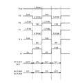
次に、この−0.5Vdd発生回路40の動作について図2(a)(b)、図3を参照しながら説明する。図3はこの−0.5Vdd発生回路40の定常状態における動作タイミング図である。
Next, the operation of the -0.5
まず、クロックφがLowレベルの時のチャージポンプ回路の動作について説明する(図2(a)、図3参照)。このとき、クロックドライバーCDのPチャネル型MOSトランジスタM6はオンし、Nチャネル型MOSトランジスタM7はオフするので、反転クロック*φはHighレベル(Vddレベル)となる。また、第1,第4のスイッチング用MOSトランジスタM1,M4をオンし、第2、第3、第5のスイッチング用MOSトランジスタM2,M3,M5をオフする。 First, the operation of the charge pump circuit when the clock φ is at the low level will be described (see FIGS. 2A and 3). At this time, the P-channel MOS transistor M6 of the clock driver CD is turned on and the N-channel MOS transistor M7 is turned off, so that the inverted clock * φ is at a high level (Vdd level). Further, the first and fourth switching MOS transistors M1 and M4 are turned on, and the second, third and fifth switching MOS transistors M2, M3 and M5 are turned off.
すると、図2(a)中の太線で示すように、クロックドライバーCDのPチャネル型MOSトランジスタM6、第1のコンデンサC1、第4のスイッチング用MOSトランジスタM4、第2のコンデンサC2、第1のスイッチング用MOSトランジスタM1、接地電圧Vssを通る経路で、第1のコンデンサC1及び第2のコンデンサC2が直列接続されて充電される。 Then, as indicated by a thick line in FIG. 2A, the P-channel MOS transistor M6, the first capacitor C1, the fourth switching MOS transistor M4, the second capacitor C2, and the first capacitor of the clock driver CD. The first capacitor C1 and the second capacitor C2 are connected in series and charged through a path passing through the switching MOS transistor M1 and the ground voltage Vss.
これにより、第1のコンデンサC1の一方の端子はVddに充電され、その他方の端子の電圧V1は+0.5Vddに充電され、第2のコンデンサC2の他方の端子の電圧V1も+0.5Vddに充電される。 As a result, one terminal of the first capacitor C1 is charged to Vdd, the voltage V1 of the other terminal is charged to + 0.5Vdd, and the voltage V1 of the other terminal of the second capacitor C2 is also + 0.5Vdd. Charged.
次に、クロックφがHighレベルの時の回路動作について説明する(図2(b)、図3参照)。このとき、クロックドライバーCDのNチャネル型MOSトランジスタM7がオンし、Pチャネル型MOSトランジスタM6がオフするため、反転クロック*φはLowレベルとなる。(Vssレベル)また、第1,第4のスイッチング用MOSトランジスタM1,M4をオフし、第2,第3,第5のスイッチング用MOSトランジスタM2,M3,M5をオンする。 Next, the circuit operation when the clock φ is at a high level will be described (see FIGS. 2B and 3). At this time, since the N-channel MOS transistor M7 of the clock driver CD is turned on and the P-channel MOS transistor M6 is turned off, the inverted clock * φ is at the low level. (Vss level) The first and fourth switching MOS transistors M1 and M4 are turned off, and the second, third and fifth switching MOS transistors M2, M3 and M5 are turned on.
すると、図2(b)中の太い破線で示すように、2つの経路から出力端子に−0.5Vddが供給される。1つの経路は、接地電圧Vssから、第3のスイッチング用MOSトランジスタM3、第2のコンデンサC2、第2のスイッチング用MOSトランジスタM2を通して、第2のコンデンサC2の電荷が放電され、出力端子に−0.5Vddが供給される。これは、第2のコンデンサC2の他方の電圧V3はクロックφがLowレベルのときに+0.5Vddに充電されているため、第3のスイッチング用MOSトランジスタM3がオンすることにより、電圧V3が+0.5VddからVssに変化することに伴って、第2のコンデンサC2の容量結合により、第2のコンデンサC2の一方の端子の電圧V2はVss(0V)から−0.5Vddに降圧されるためである。 Then, as shown by the thick broken line in FIG. 2B, −0.5 Vdd is supplied from the two paths to the output terminal. One path is that the electric charge of the second capacitor C2 is discharged from the ground voltage Vss through the third switching MOS transistor M3, the second capacitor C2, and the second switching MOS transistor M2, and − 0.5Vdd is supplied. This is because the other voltage V3 of the second capacitor C2 is charged to +0.5 Vdd when the clock φ is at a low level, and the voltage V3 becomes +0 by turning on the third switching MOS transistor M3. This is because the voltage V2 at one terminal of the second capacitor C2 is stepped down from Vss (0V) to -0.5Vdd due to the capacitive coupling of the second capacitor C2 with the change from .5Vdd to Vss. is there.
もう1つの経路は、接地電圧Vssから、クロックドライバーCDのNチャネル型MOSトランジスタM7、第1のコンデンサC1、第5のスイッチング用MOSトランジスタM5を通して、第1のコンデンサC1の電荷が放電され、出力端子に−0.5Vddが供給される。これは、クロックφがLowレベルのときに、第1のコンデンサC1の他方端子の電圧V1は+0.5Vddに充電されるが、クロックφがHighレベルに変化すると、Nチャネル型MOSトランジスタM7がオンすることにより、第1のコンデンサC1の一方の端子の電圧がVddからVssに変化することに伴い、第1のコンデンサC1の容量結合により、第1のコンデンサC1の他方の端子の電圧V1は+0.5Vddから−0.5Vddに降圧されるためである。 The other path is that the charge of the first capacitor C1 is discharged from the ground voltage Vss through the N-channel MOS transistor M7 of the clock driver CD, the first capacitor C1, and the fifth switching MOS transistor M5. -0.5 Vdd is supplied to the terminal. This is because when the clock φ is at the low level, the voltage V1 at the other terminal of the first capacitor C1 is charged to +0.5 Vdd, but when the clock φ changes to the high level, the N-channel MOS transistor M7 is turned on. Thus, as the voltage at one terminal of the first capacitor C1 changes from Vdd to Vss, the voltage V1 at the other terminal of the first capacitor C1 is +0 due to capacitive coupling of the first capacitor C1. This is because the voltage is reduced from 5 Vdd to -0.5 Vdd.
このクロックφがLowレベルの時の動作と、Highレベル時の動作を交互に繰り返すことにより、出力電圧Voutとして、電源電圧Vddを−0.5倍した−0.5Vddが得られる。 By alternately repeating the operation when the clock φ is at the low level and the operation at the high level, -0.5 Vdd obtained by multiplying the power supply voltage Vdd by -0.5 is obtained as the output voltage Vout.
このように、本実施形態によれば、−0.5Vdd発生回路40を採用したので、Nチャネル型MOSトランジスタが多用される結果、従来と同等のLED25の駆動電流mnIを得るための回路のパターン面積を小さくでき、かつ効率改善を実現している。
As described above, according to the present embodiment, since the -0.5
次に、本発明の効果をより明確にするために、−0.5Vdd発生回路40と1.5Vdd発生回路60との対比を行う。そのために、1.5Vdd発生回路60の具体的な構成について図4を参照して説明する。図4(a)は、クロックドライバーCDの入力クロックであるクロックφがHighレベルの場合、図4(b)はクロックφがLowレベルの場合を示している。
Next, in order to clarify the effect of the present invention, the -0.5
第1のスイッチング用MOSトランジスタM11のソースに電源電圧Vddが印加され、この第1のスイッチング用MOSトランジスタM11のドレインは、第2のスイッチング用MOSトランジスタM12のソースに接続されている。第1のスイッチング用MOSトランジスタM11及び第2のスイッチング用MOSトランジスタM12は、電荷転送素子として機能する。 The power supply voltage Vdd is applied to the source of the first switching MOS transistor M11, and the drain of the first switching MOS transistor M11 is connected to the source of the second switching MOS transistor M12. The first switching MOS transistor M11 and the second switching MOS transistor M12 function as charge transfer elements.
ここで、第1のスイッチング用MOSトランジスタM11及び第12のスイッチング用MOSトランジスタM2は、いずれもPチャネル型である。その理由は、第1のスイッチング用MOSトランジスタM11及び第2のスイッチング用MOSトランジスタM12をオンオフさせるための電圧を同じ回路内から得るためである。第1のスイッチング用MOSトランジスタM11及び第2のスイッチング用MOSトランジスタM12をオンさせるためにはそれらのゲートに接地電圧Vssを与えればよいし、オフさせる場合にはそれらのゲートにこの回路の出力電圧Vout(=1.5Vdd)を与えればよい。 Here, both the first switching MOS transistor M11 and the twelfth switching MOS transistor M2 are P-channel type. The reason is that a voltage for turning on and off the first switching MOS transistor M11 and the second switching MOS transistor M12 is obtained from the same circuit. In order to turn on the first switching MOS transistor M11 and the second switching MOS transistor M12, a ground voltage Vss may be applied to their gates. When they are turned off, the output voltage of this circuit is applied to their gates. Vout (= 1.5 Vdd) may be given.
また、第1のコンデンサC1の一方の端子には、クロックドライバーCDの出力が接続されている。クロックドライバーCDは、電源電圧Vddと接地電圧Vssの間に、Pチャネル型MOSトランジスタM16、Nチャネル型MOSトランジスタM17を直列に接続してCMOSインバータとして構成される。そして、クロックドライバーCDにはクロックφが印加され、このクロックφはクロックドライバーCDによって反転される。その反転クロック*φが、クロックドライバーCDの出力として第1のコンデンサC1の一方の端子に印加される。 The output of the clock driver CD is connected to one terminal of the first capacitor C1. The clock driver CD is configured as a CMOS inverter by connecting a P-channel MOS transistor M16 and an N-channel MOS transistor M17 in series between a power supply voltage Vdd and a ground voltage Vss. A clock φ is applied to the clock driver CD, and the clock φ is inverted by the clock driver CD. The inverted clock * φ is applied to one terminal of the first capacitor C1 as the output of the clock driver CD.
また、第2のコンデンサC2は、その一方の端子が第1及び第2のスイッチング用MOSトランジスタM11,M12の接続点に接続されている。第3のスイッチング用MOSトランジスタM13は、第2のコンデンサC2の他方の端子と電源電圧Vddの間に接続されている。 The second capacitor C2 has one terminal connected to the connection point of the first and second switching MOS transistors M11 and M12. The third switching MOS transistor M13 is connected between the other terminal of the second capacitor C2 and the power supply voltage Vdd.
また、第4のスイッチング用MOSトランジスタM14は、第1のコンデンサC1の他方の端子と第2のコンデンサC2の他方の端子の間に接続されている。第5のスイッチング用MOSトランジスタM15は、第1のコンデンサC1の他方の端子と第2のスイッチング用MOSトランジスタM12のドレインである出力端子に接続されている。そして、この回路は、第2のスイッチング用MOSトランジスタM12のドレインから出力電圧Vout(=1.5Vdd)を得るものである。 The fourth switching MOS transistor M14 is connected between the other terminal of the first capacitor C1 and the other terminal of the second capacitor C2. The fifth switching MOS transistor M15 is connected to the other terminal of the first capacitor C1 and the output terminal which is the drain of the second switching MOS transistor M12. This circuit obtains the output voltage Vout (= 1.5 Vdd) from the drain of the second switching MOS transistor M12.
ここで、第3及び第5のスイッチング用MOSトランジスタM13,M15はPチャネル型、第4のスイッチング用MOSトランジスタM14はNチャネル型である。第3及び第5のスイッチング用MOSトランジスタM13,M15をPチャネル型とした理由は、前述と同様に、第3のスイッチング用MOSトランジスタM13及び第5のスイッチング用MOSトランジスタM15をオンオフさせるための電圧を同じ回路内から得るためである。 Here, the third and fifth switching MOS transistors M13 and M15 are P-channel type, and the fourth switching MOS transistor M14 is N-channel type. The reason why the third and fifth switching MOS transistors M13 and M15 are of the P-channel type is the same as described above because the voltage for turning on and off the third switching MOS transistor M13 and the fifth switching MOS transistor M15 is used. Is obtained from the same circuit.
また、第1及び第2のコンデンサC1,C2は互いに等しい容量値を有しているものとする。また、第1,第2,第3,第4,第5のスイッチング用MOSトランジスタM11,M12,M13,M14,M15は、クロックφの電圧レベルに応じて、不図示の制御回路によってゲート電圧を制御することにより、後述するようにそれらのオン(ON)、オフ(OFF)が制御されている。 Further, it is assumed that the first and second capacitors C1 and C2 have the same capacitance value. The first, second, third, fourth, and fifth switching MOS transistors M11, M12, M13, M14, and M15 have their gate voltages set by a control circuit (not shown) according to the voltage level of the clock φ. By controlling, as described later, ON (ON) and OFF (OFF) are controlled.
次に、この回路の動作について図4(a)(b)、図5を参照しながら説明する。図5はこのチャージポンプ回路の定常状態における動作タイミング図である。 Next, the operation of this circuit will be described with reference to FIGS. 4 (a) and 4 (b) and FIG. FIG. 5 is an operation timing chart in the steady state of the charge pump circuit.
まず、クロックφがHighレベルの時のチャージポンプ回路の動作について説明する(図4(a)、図5参照)。このとき、クロックドライバーCDのNチャネル型MOSトランジスタM17はオンし、反転クロック*φはLowレベル(0V)となる。また、第1,第4のスイッチング用MOSトランジスタM11,M14をオンし、第2,第3,第5のスイッチング用MOSトランジスタM12,M13,M15をオフする。すると、図4(a)中の太い破線で示すように、電源電圧Vddから、第1のスイッチング用MOSトランジスタM11、第2のコンデンサC2、第4のスイッチング用MOSトランジスタM14、第1のコンデンサC1、クロックドライバーCDのNチャネル型MOSトランジスタM17を通る経路で、第1のコンデンサC1及び第2のコンデンサC2が直列接続されて充電される。これにより、第2のコンデンサC2の一方の端子の電圧V2はVddに充電され、その他方の端子の電圧V3は0.5Vddに充電され、第1のコンデンサC1の他方の端子の電圧V1も0.5Vddに充電される。 First, the operation of the charge pump circuit when the clock φ is at a high level will be described (see FIGS. 4A and 5). At this time, the N-channel MOS transistor M17 of the clock driver CD is turned on, and the inverted clock * φ is at the low level (0 V). Further, the first and fourth switching MOS transistors M11 and M14 are turned on, and the second, third and fifth switching MOS transistors M12, M13 and M15 are turned off. Then, as shown by a thick broken line in FIG. 4A, the first switching MOS transistor M11, the second capacitor C2, the fourth switching MOS transistor M14, and the first capacitor C1 are derived from the power supply voltage Vdd. The first capacitor C1 and the second capacitor C2 are connected in series and charged through a path passing through the N-channel MOS transistor M17 of the clock driver CD. As a result, the voltage V2 at one terminal of the second capacitor C2 is charged to Vdd, the voltage V3 at the other terminal is charged to 0.5Vdd, and the voltage V1 at the other terminal of the first capacitor C1 is also 0. Charged to 5Vdd.
次に、クロックφがLowレベルの時のチャージポンプ回路の動作について説明する(図4(b)、図5参照)。このとき、クロックドライバーCDのPチャネル型MOSトランジスタM7はオンし、反転クロック*φはHighレベルとなる。また、第1,第4のスイッチング用MOSトランジスタM11,M14をオフし、第2,第3,第5のスイッチング用MOSトランジスタM12,M13,M15をオンする。 Next, the operation of the charge pump circuit when the clock φ is at the low level will be described (see FIGS. 4B and 5). At this time, the P-channel type MOS transistor M7 of the clock driver CD is turned on, and the inverted clock * φ is at a high level. Further, the first and fourth switching MOS transistors M11 and M14 are turned off, and the second, third and fifth switching MOS transistors M12, M13 and M15 are turned on.
すると、図4(b)中の太い線で示すように、2つの経路から出力端子に1.5Vddが供給される。1つの経路は、電源電圧Vddから、第3のスイッチング用MOSトランジスタM13、第2のコンデンサC2、第2のスイッチング用MOSトランジスタM12を通して、第2のコンデンサC2の電荷が放電され、出力端子に1.5Vddが供給される。これは、第2のコンデンサC2の他方の電圧V12はクロックφがHighレベルのときに0.5Vddに充電されているため、第3のスイッチング用MOSトランジスタM13がオンすることにより、電圧V12が0.5VddからVddに変化することに伴って、第2のコンデンサC2の容量結合により、第2のコンデンサの一方の端子の電圧V11はVddから1.5Vddに昇圧されるためである。 Then, as indicated by a thick line in FIG. 4B, 1.5 Vdd is supplied to the output terminal from the two paths. In one path, the charge of the second capacitor C2 is discharged from the power supply voltage Vdd through the third switching MOS transistor M13, the second capacitor C2, and the second switching MOS transistor M12, and 1 is output to the output terminal. .5Vdd is supplied. This is because the other voltage V12 of the second capacitor C2 is charged to 0.5 Vdd when the clock φ is at a high level, so that the voltage V12 becomes 0 by turning on the third switching MOS transistor M13. This is because the voltage V11 at one terminal of the second capacitor is boosted from Vdd to 1.5Vdd due to the capacitive coupling of the second capacitor C2 along with the change from .5Vdd to Vdd.
もう1つの経路は、電源電圧Vddから、クロックドライバーCDのPチャネル型MOSトランジスタM16、第1のコンデンサC1、第5のスイッチング用MOSトランジスタM15を通して、第1のコンデンサC1の電荷が放電され、出力端子に1.5Vddが供給される。 The other path is that the charge of the first capacitor C1 is discharged from the power supply voltage Vdd through the P-channel MOS transistor M16, the first capacitor C1, and the fifth switching MOS transistor M15 of the clock driver CD, and the output 1.5Vdd is supplied to the terminal.
これは、クロックφがHighレベルのときに、第1のコンデンサC1の他方端子の電圧V13は0.5Vddに充電されるが、クロックφがLowレベルに変化すると、Pチャネル型MOSトランジスタM16がオンすることにより、第1のコンデンサC1の一方の端子の電圧が0VからVddに変化することに伴い、第1のコンデンサC1の容量結合により、第1のコンデンサC1の他方の端子の電圧V13は0.5Vddから1.5Vddに昇圧されるためである。 This is because when the clock φ is at a high level, the voltage V13 at the other terminal of the first capacitor C1 is charged to 0.5 Vdd, but when the clock φ changes to a low level, the P-channel MOS transistor M16 is turned on. Thus, as the voltage at one terminal of the first capacitor C1 changes from 0V to Vdd, the voltage V13 at the other terminal of the first capacitor C1 is 0 due to capacitive coupling of the first capacitor C1. This is because the voltage is boosted from 5 Vdd to 1.5 Vdd.
このクロックφがLowレベルの時の動作と、Highレベル時の動作を交互に繰り返すことにより、出力電圧Voutとして、電源電圧Vddを1.5倍した1.5Vddが得られる。 By alternately repeating the operation when the clock φ is at the low level and the operation when the clock φ is at the high level, 1.5 Vdd that is 1.5 times the power supply voltage Vdd is obtained as the output voltage Vout.
上述のように、−0.5Vdd発生回路40においては、第1、第2、第3、及び第5のスイッチング用MOSトランジスタM1,M2,M3,M5がNチャネル型であることが必要であり、1.5Vdd発生回路60では、第1、第2、第3及び第5のスイッチング用MOSトランジスタM11,M12,M13,M15がPチャネル型であることが必要であることが明らかとなった。そこで、−0.5Vdd発生回路40における第4のスイッチング用MOSトランジスタM4をPチャネル型、1.5Vdd発生回路60における第4のスイッチング用MOSトランジスタM14をNチャネル型、クロックドライバーCDはPチャネル型、Nチャネル型1個ずつから構成されるとして、2つの回路で使用されるトランジスタの種類の数を計算すると、表1のように、1.5Vdd発生回路60では、Pチャネル型が5個、Nチャネル型2個となり、−0.5Vdd発生回路40では逆に、Nチャネル型が5個、Pチャネル型2個となり、Nチャネル型が多用されている。そこで、Pチャネル型とNチャネル型のパターン面積比を3:1とすると、1.5Vdd発生回路60と−0.5Vdd発生回路40との面積比(ただし、トランジスタ部分のみ)は、17:11となる。即ち、−0.5Vdd発生回路40は1.5Vdd発生回路60に比して35%程度小さなパターン面積で形成できる。その分、駆動回路全体の面積も小さくできる。
As described above, in the −0.5
また、MOSトランジスタのゲート容量等の寄生容量を小さくできるため、駆動回路の消費電流が低減され、その効率改善を実現できる。 Further, since the parasitic capacitance such as the gate capacitance of the MOS transistor can be reduced, the current consumption of the drive circuit is reduced, and the efficiency can be improved.
なお、本発明は白色LEDに限らず、赤色LED、緑色LED、青色LED、アノードとカソードを有する他の発光素子の駆動回路にも広く適用できるものである。また、本実施形態では−0.5Vddという負電圧を発生し、電源電圧Vddとの間で1.5Vddの電位差を得ているが、負電圧の大きさは−0.5Vddに限らず、−0.4Vddあるいは−0.6Vddでもよいし、他の値であってもよい。 The present invention is not limited to white LEDs, and can be widely applied to drive circuits for red LEDs, green LEDs, blue LEDs, and other light emitting elements having an anode and a cathode. In this embodiment, a negative voltage of −0.5 Vdd is generated and a potential difference of 1.5 Vdd is obtained with respect to the power supply voltage Vdd. However, the magnitude of the negative voltage is not limited to −0.5 Vdd. It may be 0.4 Vdd or -0.6 Vdd, or another value.

M1 第1のスイッチング用MOSトランジスタ
M2 第2のスイッチング用MOSトランジスタ
M3 第3のスイッチング用MOSトランジスタ
M4 第4のスイッチング用MOSトランジスタ
M5 第5のスイッチング用MOSトランジスタ
M6 Pチャネル型MOSトランジスタ
M7 Nチャネル型MOSトランジスタ
CD クロックドライバー C1 第1のコンデンサ
C2 第2のコンデンサ 20 端子
21 端子 25 白色LED
30 クロック発生回路 40 −0.5Vdd発生回路
M1 1st switching MOS transistor M2 2nd switching MOS transistor M3 3rd switching MOS transistor M4 4th switching MOS transistor M5 5th switching MOS transistor M6 P channel type MOS transistor M7 N channel type MOS transistor
CD clock driver C1 first capacitor C2
21 terminal 25 white LED
30 clock generation circuit 40 -0.5 Vdd generation circuit
Claims (7)
前記クロックが第1の電圧レベルのときに、前記第1、第4のスイッチング素子をオンして前記第1及び第2のコンデンサを前記第1のスイッチング素子を介して前記第1の電圧レベルと接地電圧との間に直列に接続して充電し、前記クロックが第2の電圧レベルのときに、前記第5のスイッチング素子をオンして、前記第1のコンデンサを接地電圧と前記出力端子との間に接続して放電すると共に、前記第2及び第3のスイッチング素子をオンして前記第2のコンデンサを前記第2のスイッチング素子を介して接地電圧と前記出力端子との間に接続して放電し、
少なくとも前記第1、第2、第3及び第5のスイッチング素子をNチャネル型MOSトランジスタで構成したことを特徴とする請求項2に記載の駆動回路。 The negative voltage generation circuit includes a first switching element having a ground voltage applied to an input terminal, a second switching element connected in series with the first switching element, and a clock supplied to one terminal. A first capacitor, a second capacitor having one terminal connected to a connection point between the first switching element and the second switching element, and the other terminal of the second capacitor and a ground voltage A third switching element connected between the first capacitor, a fourth switching element connected between the other terminal of the first capacitor and the other terminal of the second capacitor, and the first capacitor. And a fifth switching element connected to the output terminal of the second switching element,
When the clock is at the first voltage level, the first and fourth switching elements are turned on to connect the first and second capacitors to the first voltage level via the first switching element. The first switching capacitor is turned on when the clock is at the second voltage level, and the first capacitor is connected to the ground voltage and the output terminal. And the second switching element is turned on and the second capacitor is connected between the ground voltage and the output terminal via the second switching element. Discharge
3. The drive circuit according to claim 2, wherein at least the first, second, third, and fifth switching elements are configured by N-channel MOS transistors.
Priority Applications (5)
| Application Number | Priority Date | Filing Date | Title |
|---|---|---|---|
| JP2004097607A JP2005284710A (en) | 2004-03-30 | 2004-03-30 | Driving circuit |
| TW094108305A TWI291684B (en) | 2004-03-30 | 2005-03-18 | Drive circuit |
| US11/091,342 US7463236B2 (en) | 2004-03-30 | 2005-03-29 | Driver circuit |
| KR1020050025813A KR100729702B1 (en) | 2004-03-30 | 2005-03-29 | Driving circuit |
| CNA2005100629067A CN1677861A (en) | 2004-03-30 | 2005-03-30 | Driver circuit |
Applications Claiming Priority (1)
| Application Number | Priority Date | Filing Date | Title |
|---|---|---|---|
| JP2004097607A JP2005284710A (en) | 2004-03-30 | 2004-03-30 | Driving circuit |
Publications (2)
| Publication Number | Publication Date |
|---|---|
| JP2005284710A true JP2005284710A (en) | 2005-10-13 |
| JP2005284710A5 JP2005284710A5 (en) | 2007-03-29 |
Family
ID=35050202
Family Applications (1)
| Application Number | Title | Priority Date | Filing Date |
|---|---|---|---|
| JP2004097607A Withdrawn JP2005284710A (en) | 2004-03-30 | 2004-03-30 | Driving circuit |
Country Status (5)
| Country | Link |
|---|---|
| US (1) | US7463236B2 (en) |
| JP (1) | JP2005284710A (en) |
| KR (1) | KR100729702B1 (en) |
| CN (1) | CN1677861A (en) |
| TW (1) | TWI291684B (en) |
Cited By (2)
| Publication number | Priority date | Publication date | Assignee | Title |
|---|---|---|---|---|
| JP2009038218A (en) * | 2007-08-01 | 2009-02-19 | Denso Corp | Light emitting diode drive circuit |
| JP2009290592A (en) * | 2008-05-29 | 2009-12-10 | Fujitsu Ltd | Drive circuit and optical switch |
Families Citing this family (7)
| Publication number | Priority date | Publication date | Assignee | Title |
|---|---|---|---|---|
| US7076225B2 (en) * | 2001-02-16 | 2006-07-11 | Qualcomm Incorporated | Variable gain selection in direct conversion receiver |
| TWI273725B (en) * | 2004-10-13 | 2007-02-11 | Richtek Technology Corp | Charge pump applied to LED driving circuit |
| KR101219036B1 (en) * | 2005-05-02 | 2013-01-07 | 삼성디스플레이 주식회사 | Organic light emitting diode display |
| US7816975B2 (en) * | 2005-09-20 | 2010-10-19 | Hewlett-Packard Development Company, L.P. | Circuit and method for bias voltage generation |
| KR20130086847A (en) * | 2012-01-26 | 2013-08-05 | 삼성전자주식회사 | Low power circuit for reducing leakage power using negative voltage |
| EP2642823B1 (en) | 2012-03-24 | 2016-06-15 | Dialog Semiconductor GmbH | Method for optimizing efficiency versus load current in an inductive boost converter for white LED driving |
| US10075139B2 (en) * | 2016-11-08 | 2018-09-11 | Stmicroelectronics, Inc. | Linear high voltage driver with programmable differential and common mode gain |
Family Cites Families (9)
| Publication number | Priority date | Publication date | Assignee | Title |
|---|---|---|---|---|
| US5914869A (en) | 1997-09-15 | 1999-06-22 | General Instrument Corporation | Ac/dc transformerless voltage converter |
| KR100377698B1 (en) * | 1999-12-08 | 2003-03-29 | 산요 덴키 가부시키가이샤 | Charge-pump circuit |
| JP3475173B2 (en) | 1999-12-08 | 2003-12-08 | 三洋電機株式会社 | Charge pump circuit |
| JP3671012B2 (en) * | 2002-03-07 | 2005-07-13 | 三洋電機株式会社 | Display device |
| KR100455991B1 (en) * | 2002-08-28 | 2004-11-08 | 삼성전자주식회사 | Apparatus for controlling lcd backlight in mobile station |
| TW555350U (en) | 2002-08-29 | 2003-09-21 | Prec Instr Dev Ct Nat S | Low voltage driving lighting, false-proof distinguishing and indicating light-emitting device |
| JP3949040B2 (en) * | 2002-09-25 | 2007-07-25 | 東北パイオニア株式会社 | Driving device for light emitting display panel |
| JP2004179138A (en) * | 2002-10-01 | 2004-06-24 | Sanyo Electric Co Ltd | Electroluminescent display device and manufacturing method thereof |
| TWI253042B (en) * | 2003-05-14 | 2006-04-11 | Au Optronics Corp | Driving method and pixel structure of active matrix type LCD panel |
-
2004
- 2004-03-30 JP JP2004097607A patent/JP2005284710A/en not_active Withdrawn
-
2005
- 2005-03-18 TW TW094108305A patent/TWI291684B/en not_active IP Right Cessation
- 2005-03-29 KR KR1020050025813A patent/KR100729702B1/en not_active IP Right Cessation
- 2005-03-29 US US11/091,342 patent/US7463236B2/en not_active Expired - Fee Related
- 2005-03-30 CN CNA2005100629067A patent/CN1677861A/en active Pending
Cited By (2)
| Publication number | Priority date | Publication date | Assignee | Title |
|---|---|---|---|---|
| JP2009038218A (en) * | 2007-08-01 | 2009-02-19 | Denso Corp | Light emitting diode drive circuit |
| JP2009290592A (en) * | 2008-05-29 | 2009-12-10 | Fujitsu Ltd | Drive circuit and optical switch |
Also Published As
| Publication number | Publication date |
|---|---|
| KR100729702B1 (en) | 2007-06-19 |
| CN1677861A (en) | 2005-10-05 |
| TW200539098A (en) | 2005-12-01 |
| TWI291684B (en) | 2007-12-21 |
| US20050218970A1 (en) | 2005-10-06 |
| KR20060044893A (en) | 2006-05-16 |
| US7463236B2 (en) | 2008-12-09 |
Similar Documents
| Publication | Publication Date | Title |
|---|---|---|
| JP4557577B2 (en) | Charge pump circuit | |
| KR100729702B1 (en) | Driving circuit | |
| KR20060045807A (en) | Driving circuit | |
| US8970575B2 (en) | Power source circuit and liquid crystal display apparatus having the same | |
| TWI716160B (en) | Pixel circuit | |
| JP4284345B2 (en) | Voltage conversion circuit and display device including the voltage conversion circuit | |
| JP2009109881A (en) | Source driver and liquid crystal display device using same | |
| JP4969322B2 (en) | Voltage generating circuit and image display device including the same | |
| JP2008243281A (en) | Power voltage generating circuit | |
| CN113487992A (en) | Pixel circuit, light-emitting chip, display substrate and display device | |
| US20050200622A1 (en) | Power supply circuit, driver IC using the power supply circuit, liquid crystal display device, and electronic instrument | |
| US10152937B2 (en) | Semiconductor device, power supply circuit, and liquid crystal display device | |
| TWI522985B (en) | Charge pump circuit | |
| JP2007129828A (en) | Charge pump circuit | |
| JP4788826B2 (en) | Power supply | |
| JP5721444B2 (en) | Source driver and liquid crystal display device using the same | |
| KR100925326B1 (en) | DC-DC Converter | |
| US20170126117A1 (en) | Semiconductor device with booster part, and booster | |
| JP4474709B2 (en) | Power supply | |
| JP2005117830A (en) | Charge pump circuit | |
| US20240106434A1 (en) | Output buffer circuit, charge pump device, display drive device, and display device | |
| KR101065506B1 (en) | Cross-coupled type DC-DC converter | |
| JP2001245468A (en) | Booster circuit | |
| JP2005102375A (en) | Charge pump circuit | |
| JP2002058237A (en) | Charge pump circuit and its control method |
Legal Events
| Date | Code | Title | Description |
|---|---|---|---|
| A521 | Written amendment |
Free format text: JAPANESE INTERMEDIATE CODE: A523 Effective date: 20070208 |
|
| A621 | Written request for application examination |
Free format text: JAPANESE INTERMEDIATE CODE: A621 Effective date: 20070208 |
|
| A761 | Written withdrawal of application |
Free format text: JAPANESE INTERMEDIATE CODE: A761 Effective date: 20090706 |