JP2005242264A - Transparent conductivity thin film laminated body and optical filter for plasma display panel using it - Google Patents
Transparent conductivity thin film laminated body and optical filter for plasma display panel using it Download PDFInfo
- Publication number
- JP2005242264A JP2005242264A JP2004055546A JP2004055546A JP2005242264A JP 2005242264 A JP2005242264 A JP 2005242264A JP 2004055546 A JP2004055546 A JP 2004055546A JP 2004055546 A JP2004055546 A JP 2004055546A JP 2005242264 A JP2005242264 A JP 2005242264A
- Authority
- JP
- Japan
- Prior art keywords
- thin film
- transparent conductive
- conductive thin
- layer
- silver
- Prior art date
- Legal status (The legal status is an assumption and is not a legal conclusion. Google has not performed a legal analysis and makes no representation as to the accuracy of the status listed.)
- Withdrawn
Links
Images

Abstract
Description
本発明は、高透過性、低抵抗な透明導電性薄膜積層体に関する。さらには、透明導電性薄膜積層体を用いたプラズマディスプレイパネル用光学フィルターに関する。 The present invention relates to a transparent conductive thin film laminate having high permeability and low resistance. Furthermore, it is related with the optical filter for plasma display panels using a transparent conductive thin film laminated body.
透明導電性薄膜は、透明であるにも関わらず導電性を有する薄膜であり、その代表例はインジウムとスズの酸化物(ITO)からなる薄膜である。その用途は幅広く、主な用途として、表示パネルの透明電極用や電磁波遮断用に用いられている。 A transparent conductive thin film is a thin film having conductivity despite being transparent, and a typical example thereof is a thin film made of an oxide of indium and tin (ITO). Its application is wide and it is mainly used for transparent electrodes of display panels and electromagnetic wave shielding.
近年、社会が高度化するに従って、光エレクトロニクス関連部品、機器は著しく進歩しており、表示パネルの大型化や薄型化、小型携帯化のニーズが非常に高まっている。これを実現する為には、表示素子の低消費電力化が必要である。この目的の為には、可視光線透過率を維持しつつ、抵抗値が低い透明導電性薄膜の開発が有効である。特に、最近開発されつつある有機エレクトロルミネッセンス素子は、自発光タイプで、小型携帯端末向けに主に開発されており、透明導電性薄膜の低抵抗化への期待は大きい。また、現在市場に広まりつつあるプラズマディスプレイパネルや次世代のディスプレイとして開発されつつあるフィールドエミッションディスプレイに関しても、消費電力の面から低抵抗透明導電性薄膜の開発に対する期待は大きい。 In recent years, with the advancement of society, optoelectronics-related parts and devices have made remarkable progress, and the need for increasing the size and thickness of display panels and making them smaller and more portable is increasing. In order to realize this, it is necessary to reduce the power consumption of the display element. For this purpose, it is effective to develop a transparent conductive thin film having a low resistance value while maintaining visible light transmittance. In particular, the organic electroluminescence element that is being developed recently is a self-luminous type and has been developed mainly for small portable terminals, and there is a great expectation for reducing the resistance of the transparent conductive thin film. In addition, with respect to plasma display panels that are now spreading to the market and field emission displays that are being developed as next-generation displays, there are great expectations for the development of low-resistance transparent conductive thin films in terms of power consumption.
透明導電性薄膜積層体が、このようなディスプレイといった一般的用途として用いられる場合、電磁波遮断が重要な課題となってくる。電磁波は、計器に障害を及ぼすことが知られており、最近では、人体にも障害を及ぼす可能性もあるとの報告もされている。このため、電磁波放出に関しては、法的も規制される方向になっている。例えば、現在日本では、VCCI(Voluntaly Control Council for Interference by data processing equipment electronic office machine)による規制があり、米国では、FCC(Federal Communication Commission)による製品規制がある。 When the transparent conductive thin film laminate is used as a general application such as such a display, electromagnetic wave shielding becomes an important issue. Electromagnetic waves are known to cause damage to instruments, and recently it has been reported that they may also damage the human body. For this reason, legal regulations are also being imposed on electromagnetic wave emission. For example, in Japan, there is a regulation by VCCI (Voluntary Control Council for Interference by data processing equipment electronic machinery machine), and in the United States by FCC (Federal Communications).
電磁波遮断用として透明導電性薄膜積層体が用いられている例として、テレビやコンピューター用CRTモニター向けの電磁波遮断フィルターがある。テレビ用途として最近、急速に普及が進んでいるプラズマディスプレイパネルは、その発光原理上、強度の電磁波を表示部分から外部に放出する。強度の電磁波を遮断する為には、低抵抗であり、透明な電磁波遮断フィルターが必要となる。電磁波遮断フィルターのひとつとして、透明導電性薄膜タイプの光学フィルターがあるが、その電磁波遮断能力は、光学フィルターの面抵抗が低いほど優れる傾向がある。 As an example in which a transparent conductive thin film laminate is used for electromagnetic wave shielding, there is an electromagnetic wave shielding filter for a CRT monitor for a television or a computer. Recently, plasma display panels, which have been rapidly spread as television applications, emit strong electromagnetic waves from the display portion to the outside due to the principle of light emission. In order to block strong electromagnetic waves, a low resistance and transparent electromagnetic wave blocking filter is required. As one of the electromagnetic wave shielding filters, there is a transparent conductive thin film type optical filter, but the electromagnetic wave shielding ability tends to be more excellent as the surface resistance of the optical filter is lower.
低抵抗な光学フィルターを実現可能とする低抵抗な透明導電性薄膜の開発にあたっては、抵抗が低い金属薄膜層を積層して透明導電性薄膜を得ることが通常行われる。金属薄膜層として、特に純物質中でも最も比抵抗が小さい銀を用いた金属薄膜層の利用が有効である。さらに、透過率の上昇及び金属薄膜層の安定性向上には、金属薄膜層を透明高屈折率薄膜層、例えば、前述のITO層で挟み、透明導電性薄膜積層体を形成することが非常に有効である。この透明導電性薄膜積層体は、各薄膜層の材料や膜厚を選ぶことによって、用途に応じて最適な光学特性及び電気特性を有するように設計することが可能である。 In developing a low-resistance transparent conductive thin film capable of realizing a low-resistance optical filter, it is usually performed to obtain a transparent conductive thin film by laminating metal thin film layers having low resistance. As the metal thin film layer, it is particularly effective to use a metal thin film layer using silver having the smallest specific resistance among pure substances. Furthermore, in order to increase the transmittance and improve the stability of the metal thin film layer, it is very important to form a transparent conductive thin film laminate by sandwiching the metal thin film layer with a transparent high refractive index thin film layer, for example, the aforementioned ITO layer. It is valid. This transparent conductive thin film laminate can be designed to have optimum optical characteristics and electrical characteristics according to the application by selecting the material and film thickness of each thin film layer.
しかし、比抵抗が低いことから金属薄膜層材料として好適に用いられる銀は、原子の凝集を生じやすいことが知られている。例えば、塩化物イオンの存在下においては、容易に凝集を生じる。銀薄膜中の銀原子が凝集すると、銀白色の点を生じ、本来持つ高透明性や、低抵抗性を失う結果となる。ITO層と銀層からなる透明導電性薄膜積層体は、銀の単独層に比べると塩素イオンに対する耐久性が向上しているが、近年、上記のディスプレイ装置が民生用として急激に普及し始めていることから、より塩化物イオンに対して高耐久な透明導電性薄膜積層体の開発が求められ、且つ、期待されている。 However, it is known that silver, which is suitably used as a metal thin film layer material, tends to cause atomic aggregation because of its low specific resistance. For example, aggregation easily occurs in the presence of chloride ions. Aggregation of silver atoms in the silver thin film produces a silver-white spot, resulting in the loss of inherent high transparency and low resistance. The transparent conductive thin film laminate comprising an ITO layer and a silver layer has improved durability against chlorine ions compared to a single silver layer, but in recent years, the above display device has begun to spread rapidly for consumer use. Therefore, development of a transparent conductive thin film laminate that is more durable against chloride ions is required and expected.
銀の凝集を抑制する為の手法の1つとして、銀を合金化する方法がある。合金化に用いる金属としては、金、銅、パラジウムが一般的に知られており、例えば、特開平10−24520号公報(特許文献1)等の報告があり、銀以外の金属の含有率が高いほどその耐久性が向上することが知られている。しかし、他種金属の含有率が増加するとともに、銀合金とITOとの透明導電性薄膜積層体は、面抵抗の上昇及び透過率の低下を生じる傾向がある。このため、銀とITOからなる透明導電性薄膜積層体の低抵抗及び高透過率をできる限り維持したまま耐久性を向上させる技術が求められている。 One method for suppressing the aggregation of silver is to alloy silver. As metals used for alloying, gold, copper, and palladium are generally known. For example, there is a report such as Japanese Patent Laid-Open No. 10-24520 (Patent Document 1), and the content of metals other than silver is It is known that the higher the durability, the higher the durability. However, as the content of other metals increases, the transparent conductive thin film laminate of silver alloy and ITO tends to cause an increase in sheet resistance and a decrease in transmittance. For this reason, there is a demand for a technique for improving durability while maintaining the low resistance and high transmittance of the transparent conductive thin film laminate made of silver and ITO as much as possible.
また、ITOとAgの組合せからなる透明導電性薄膜をは、低い面抵抗を実現しようとすると、波長が400〜500nm及び600〜700nmの光の透過率が500〜600nmの透過率に比較して低く、可視光線透過率の面でも不利となる傾向がある。一方、PDP光学フィルター用途に透明導電性薄膜を利用する場合、透明導電性薄膜は可視光全域にわたって、できるだけ均一で高い透過率を示すことが、フィルターとしての光学設計等の自由度を高くすることが出来る。このため、透過スペクトルが可視光領域において、よりフラット、かつ、高透過である透明導電性薄膜積層体の出現が望まれている。
従って、本発明が解決しようとする課題は、透過率の波長依存性が少なく、より具体的には400〜500nm、500〜600nm、600〜700nmのそれぞれの領域における透過率の比が従来に比較して著しく小さく、かつ、塩素イオン等に対する耐久性が従来と比較して著しく高い低面抵抗の透明導電性薄膜積層体を提供することである。さらには、従来よりも調色が容易かつ鮮明な、環境に対して高耐久なプラズマディスプレイパネル用光学フィルターを提供することである。 Therefore, the problem to be solved by the present invention is that the wavelength dependency of the transmittance is small, and more specifically, the transmittance ratio in each region of 400 to 500 nm, 500 to 600 nm, and 600 to 700 nm is compared with the conventional one. Thus, it is to provide a transparent conductive thin film laminate having a low sheet resistance which is remarkably small and has a significantly higher durability against chlorine ions or the like than conventional ones. It is another object of the present invention to provide an optical filter for a plasma display panel, which is easier and clearer than conventional ones and has high durability against the environment.
本発明の課題を解決するための手段として、高屈折率層としてインジウムとセリウムと酸素からなる薄膜層を採用することにより、高屈折率層に隣接する銀主体の合金金属薄膜層の“やけ”を防止でき、その結果得られたフラットなスペクトル形状かつ高い透過率、さらに高い導電性を維持した透明導電性薄膜積層体を得ることができることを見出した。すなわち、本発明は、
(1)少なくともインジウムとセリウムと酸素からなる高屈折率層(a)と、
銀もしくは銀合金からなる金属薄膜層(b)とが、
両者の合計で5層〜13層繰り返して積層し、該金属薄膜層(b)の内、2つの主表面のそれぞれに最も近い金属薄膜層をそれぞれ(bL)、(bH)として、
金属薄膜層(bL)の膜厚と金属薄膜層(bH)の膜厚とが異なることを特徴とする透明導電性薄膜積層体であり、
(2)好ましくは、銀合金が、金、銅、パラジウム、プラチナ、ネオジウム、ビスマスから選ばれる少なくとも1種の金属を含む銀合金であることを特徴とする透明導電性薄膜積層体であり、
(3) 好ましくは、高屈折率層(a)のセリウムの含有率が、0.1wt%以上、30.0wt%以下であることを特徴とする請求項1に記載の透明導電性薄膜積層体であり、
(4) 好ましくは、金属薄膜層(b)のパラジウム含有率が0.1wt%以上、3.0wt%以下であり、銅の含有率が0.1wt%以上、3.0wt%以下であることを特徴とする透明導電性薄膜積層体であり、
(5) 好ましくは、金属薄膜層(b)のネオジウム含有率が0.1wt%以上、3.0wt%以下であり、金の含有率が0.1wt%以上、3.0wt%以下であることを特徴とする透明導電性薄膜積層体であり、
(6) 上記の透明導電性薄膜積層体を用いたプラズマディスプレイパネル用光学フィルターである。
As a means for solving the problems of the present invention, by adopting a thin film layer made of indium, cerium, and oxygen as a high refractive index layer, “burning” of a silver-based alloy metal thin film layer adjacent to the high refractive index layer is achieved. It has been found that a transparent conductive thin film laminate that maintains the flat spectrum shape, high transmittance, and high conductivity obtained as a result can be obtained. That is, the present invention
(1) a high refractive index layer (a) comprising at least indium, cerium and oxygen;
A metal thin film layer (b) made of silver or a silver alloy,
A total of 5 to 13 layers is repeatedly laminated, and among the metal thin film layers (b), the metal thin film layers closest to each of the two main surfaces are (b L ) and (b H ), respectively.
A transparent conductive thin film laminate, wherein the film thickness of the metal thin film layer (b L ) and the film thickness of the metal thin film layer (b H ) are different,
(2) Preferably, the silver alloy is a silver alloy containing at least one metal selected from gold, copper, palladium, platinum, neodymium, and bismuth, and is a transparent conductive thin film laminate,
(3) Preferably, the cerium content of the high refractive index layer (a) is 0.1 wt% or more and 30.0 wt% or less, The transparent conductive thin film laminate according to claim 1, And
(4) Preferably, the metal thin film layer (b) has a palladium content of 0.1 wt% or more and 3.0 wt% or less, and a copper content of 0.1 wt% or more and 3.0 wt% or less. A transparent conductive thin film laminate characterized by
(5) Preferably, the neodymium content of the metal thin film layer (b) is 0.1 wt% or more and 3.0 wt% or less, and the gold content is 0.1 wt% or more and 3.0 wt% or less. A transparent conductive thin film laminate characterized by
(6) An optical filter for a plasma display panel using the transparent conductive thin film laminate.
本発明により、高い導電性を維持したまま銀を主体とする金属薄膜層で銀白色の点を生じにくい高耐久な透明導電性薄膜積層体が可能となり、また、可視光領域においてフラットな透過スペクトルを有し、より高い透明性を示す透明導電性薄膜積層体を実現できる。さらには、該透明導電性薄膜積層体を用いることにより、調色が容易、かつ、多彩な調色が可能な高耐久プラズマディスプレイパネル用光学フィルターを提供することができる。このため、本発明の工業的価値は大きい。 According to the present invention, a highly durable transparent conductive thin film laminate in which silver white spots are hardly generated in a metal thin film layer mainly composed of silver while maintaining high conductivity can be obtained, and a flat transmission spectrum can be obtained in the visible light region. And a transparent conductive thin film laminate exhibiting higher transparency can be realized. Furthermore, by using the transparent conductive thin film laminate, it is possible to provide an optical filter for a highly durable plasma display panel that is easy to color and capable of various tones. For this reason, the industrial value of the present invention is great.
本発明における透明導電性薄膜積層体は、インジウムとセリウムと酸素が含まれている高屈折率層(a)と銀もしくは銀を主体とした合金(銀合金)からなる金属薄膜層(b)を繰り返し積層し、特定の2層の膜厚が特定の関係になっていることを特徴とするものである。積層体を形成する理由としては、透明導電性薄膜をプラズマディスプレイパネルやフィールドエミッションパネルなどの光学フィルターとして使用する際に求められる高い導電性と高い透明性を得るには、上記積層体構造を有することが有力な解決手段であるためである。 The transparent conductive thin film laminate in the present invention comprises a high refractive index layer (a) containing indium, cerium and oxygen and a metal thin film layer (b) made of silver or an alloy mainly composed of silver (silver alloy). It is characterized by being repeatedly laminated and having a specific relationship between the film thicknesses of two specific layers. The reason why the laminate is formed is that the above-described laminate structure is used to obtain high conductivity and high transparency required when the transparent conductive thin film is used as an optical filter such as a plasma display panel or a field emission panel. This is because this is an effective solution.
また、本発明の透明導電性薄膜積層体は、自立膜として扱いにくい場合があるので、透明基体(A)上に上記薄膜積層体を形成したものが、種々の用途に用いる上で好ましい形態である。 In addition, since the transparent conductive thin film laminate of the present invention may be difficult to handle as a self-supporting film, the thin film laminate formed on the transparent substrate (A) is a preferred form for use in various applications. is there.
本発明における透明導電性薄膜積層体の層数は、上記の高屈折率層(a)と金属薄膜層(b)との合計で、5層〜13層を有していることを特徴とする。本発明の透明導電性薄膜積層体の具体的な例示としては、透明基体(A)上に高屈折率層(a)と金属薄膜層(b)が、(a)/(b)の順の積層単位を2〜6回繰り返して積層され、さらに金属薄膜層(b)上に高屈折率層(a)が積層された様な構成である。高屈折率層(a)と金属薄膜層(b)との積層数は、多いほど導電性-透過性バランスの観点からは好ましいが、コスト、品質安定性問題を考慮すると、好ましくは11層以下、より好ましくは9層以下、特に好ましくは、7層以下である。なお、各層の間及び最表面には、様々な機能層を有しても構わない。想定される機能層としては、密着層、ガスバリア層、耐環境性向上のための層などである。 The transparent conductive thin film laminate in the present invention is characterized in that the total number of the high refractive index layer (a) and the metal thin film layer (b) has 5 to 13 layers. . As a specific example of the transparent conductive thin film laminate of the present invention, the high refractive index layer (a) and the metal thin film layer (b) are in the order of (a) / (b) on the transparent substrate (A). The stacking unit is repeated 2 to 6 times, and the high refractive index layer (a) is further stacked on the metal thin film layer (b). The higher the number of layers of the high refractive index layer (a) and the metal thin film layer (b), the better from the viewpoint of the conductivity-transmittance balance, but preferably 11 layers or less in view of cost and quality stability problems. , More preferably 9 layers or less, particularly preferably 7 layers or less. In addition, you may have a various functional layer between each layer and the outermost surface. Possible functional layers include an adhesion layer, a gas barrier layer, and a layer for improving environmental resistance.
本発明に用いられる透明基体(A)としては、主にフィルム状及び板状のものであり、透明性に優れ、用途に応じた十分な機械的強度を有するものであることが好ましい。ここで言う透明性に優れるとは、使用される状態での厚さにおいて、視感透過率が40%以上であることを示す(測定法:JIS R3106)。また、透明基体(A)の主面に、反射防止層や防眩層が形成されていても構わない。 The transparent substrate (A) used in the present invention is mainly in the form of a film and a plate, and is preferably excellent in transparency and having sufficient mechanical strength depending on the application. The term “excellent transparency” as used herein means that the luminous transmittance is 40% or more in the thickness in a used state (measurement method: JIS R3106). Further, an antireflection layer or an antiglare layer may be formed on the main surface of the transparent substrate (A).
透明基体(A)として、例えば透明基体用フィルムを用いる場合、高分子フィルムが好適に用いられる。具体的に例示すると、ポリイミド、ポリスルホン、ポリエーテルスルホン、ポリエチレンテレフタレート、ポリメチレンメタクリレート、ポリカーボネート、ポリエーテルエーテルケトン、ポリプロピレン、トリアセチルセルロース等のフィルムが挙げられる。中でも、ポリエチレンテレフタレート及びトリアセチルセルロースのフィルムが好適に用いられる。 For example, when a transparent substrate film is used as the transparent substrate (A), a polymer film is preferably used. Specific examples include films of polyimide, polysulfone, polyethersulfone, polyethylene terephthalate, polymethylene methacrylate, polycarbonate, polyetheretherketone, polypropylene, triacetylcellulose, and the like. Among these, polyethylene terephthalate and triacetyl cellulose films are preferably used.
透明基体用のフィルムの厚さに特に制限はない。通常は、20μm〜500μm程度である。 There is no particular limitation on the thickness of the film for the transparent substrate. Usually, it is about 20 μm to 500 μm.
板状の透明基体としては、高分子成形体及びガラス等が挙げられる。透明高分子成形体は、ガラスと比較して、軽い、割れにくい等の好ましい特徴がある。好ましい材料を例示すると、ポリメタクリル酸メチルをはじめとするアクリル樹脂、ポリカーボネート樹脂等が挙げられるが、これらの樹脂に限定されるものではない。中でも、ポリメタクリル酸メチルは、その広い波長領域での高透明性と機械的強度の高さから好適に使用することができる。 Examples of the plate-like transparent substrate include a polymer molded body and glass. The transparent polymer molded body has preferable characteristics such as lightness and resistance to cracking compared to glass. Examples of preferred materials include acrylic resins such as polymethyl methacrylate, polycarbonate resins, and the like, but are not limited to these resins. Among them, polymethyl methacrylate can be suitably used because of its high transparency and high mechanical strength in a wide wavelength region.
また、透明高分子成形体には、表面の硬度、耐傷付き性や密着性を増す等の理由でハードコート層が設けられることが多い。 In addition, the transparent polymer molded body is often provided with a hard coat layer for reasons such as increasing surface hardness, scratch resistance and adhesion.
ガラスは、熱及び湿気による形状変化が少ない為、微妙な精度を必要とする光学用途に対して好適に用いられる。機械的強度を持たせるために、化学強化加工、または、風冷強化加工を行い、半強化ガラスまたは強化ガラスにして通常用いられる。 Glass is suitably used for optical applications that require subtle accuracy because of little change in shape due to heat and moisture. In order to give mechanical strength, chemical tempering processing or air-cooling tempering processing is performed, and it is usually used as semi-tempered glass or tempered glass.
板状透明基体の厚さに特に制限はなく、十分な機械的強度と平面性を維持する剛性が得られれば良い。通常は、0.5mm〜10mm程度である。 There is no restriction | limiting in particular in the thickness of a plate-shaped transparent base | substrate, The rigidity which maintains sufficient mechanical strength and planarity should just be acquired. Usually, it is about 0.5 mm to 10 mm.
高屈折率層に用いられる材料としては、一般的にできるだけ透明性に優れたものであることが好ましい。ここでいう透明性に優れるとは、膜厚100nm程度の薄膜を形成した時に、その薄膜の視感透過率が60%以上、好ましくは、70%以上であることを指す(測定法:JIS R3016)。また、高屈折率材料とは、550nmの光に対する屈折率が1.4以上、好ましくは、1.8以上の材料である。これらには、用途に応じて不純物を混入させても良い。 In general, it is preferable that the material used for the high refractive index layer is as excellent in transparency as possible. The term “excellent transparency” as used herein means that when a thin film having a thickness of about 100 nm is formed, the luminous transmittance of the thin film is 60% or more, preferably 70% or more (measurement method: JIS R3016). ). The high refractive index material is a material having a refractive index with respect to light of 550 nm of 1.4 or more, preferably 1.8 or more. These may be mixed with impurities depending on the application.
本発明の高屈折率層(a)は、インジウム、セリウムと酸素が含まれている。本発明の高屈折率層(a)中のセリウムの含有率は、0.1wt%以上、30.0wt%以下であることが好ましい。より好ましくは、5.0wt%以上、20.0wt%以下である。 The high refractive index layer (a) of the present invention contains indium, cerium and oxygen. The cerium content in the high refractive index layer (a) of the present invention is preferably 0.1 wt% or more and 30.0 wt% or less. More preferably, it is 5.0 wt% or more and 20.0 wt% or less.
高屈折率層(a)の形成に関しては、イオンプレーティング法、または、反応性スパッタリング法が好適に用いられるが、これに限定されるものではなく、公知の薄膜形成法を制限無く用いることが出来る。上記のイオンプレーティング法では、反応ガスプラズマ中で所望の金属、または、焼結体を抵抗加熱したり、電子ビームにより加熱したりすることにより真空蒸着を行う。また、反応性スパッタリング法では、ターゲットに所望の金属、または、焼結体を使用、スパッタリングガスにアルゴン、ネオン等の不活性ガスを用い、反応に必要なガスを加えてスパッタリングを行う。 For the formation of the high refractive index layer (a), an ion plating method or a reactive sputtering method is preferably used, but the method is not limited to this, and a known thin film forming method can be used without limitation. I can do it. In the ion plating method described above, vacuum deposition is performed by resistance heating a desired metal or sintered body in a reactive gas plasma or heating with an electron beam. In the reactive sputtering method, a desired metal or a sintered body is used as a target, an inert gas such as argon or neon is used as a sputtering gas, and sputtering is performed by adding a gas necessary for the reaction.
本発明における高屈折率層(a)の厚さに関しては、本発明の目的を損なわない限りは特に制限はない。膜厚は、通常、透明導電性薄膜積層体の透過性及び電気伝導性を考慮して決定される。一般的には0.5nm〜100nm程度である。 The thickness of the high refractive index layer (a) in the present invention is not particularly limited as long as the object of the present invention is not impaired. The film thickness is usually determined in consideration of the transparency and electrical conductivity of the transparent conductive thin film laminate. Generally, it is about 0.5 nm to 100 nm.
金属薄膜層(b)の材料は、銀もしくは銀を主体とした合金である。銀合金の銀以外の金属としては、公知の物を用いることが出来る。好ましくは金、銅、パラジウム、プラチナ、ネオジウム、ビスマスから選ばれる1種類以上の金属を例示できる。特に、銀とパラジウムと銅との合金、銀とネオジウムと金との合金、及び、銀とネオジウムと銅との合金が好ましい。 The material of the metal thin film layer (b) is silver or an alloy mainly composed of silver. As the metal other than silver of the silver alloy, known materials can be used. Preferably, one or more kinds of metals selected from gold, copper, palladium, platinum, neodymium, and bismuth can be exemplified. In particular, an alloy of silver, palladium, and copper, an alloy of silver, neodymium, and gold, and an alloy of silver, neodymium, and copper are preferable.
本発明における銀合金に関して、上記の様な銀以外の金属の含有率が高ければ高い程透明導電性薄膜積層体の耐久性は一般的に高くなるが、透過率は低下し、面抵抗は上昇する傾向がある。このため、通常は用途に応じて必要な透過率及び面抵抗を考慮した上で、各含有率を決定する。 Regarding the silver alloy in the present invention, the higher the content of the metal other than silver as described above, the higher the durability of the transparent conductive thin film laminate generally, but the transmittance decreases and the sheet resistance increases. Tend to. For this reason, usually each content rate is determined in consideration of the required transmittance and surface resistance depending on the application.
銀とパラジウムと銅を含む合金に関して、パラジウムと銅の好ましい含有割合は、パラジウムが0.1wt%以上、3.0wt%以下であり、銅が0.1wt%以上、3.0wt%以下である。より好ましいパラジウムと銅との含有割合は、パラジウムが0.1wt%以上、1.5wt%以下、銅が0.1wt%以上、1.5wt%以下である。 Regarding the alloy containing silver, palladium and copper, the preferable content ratio of palladium and copper is 0.1 wt% or more and 3.0 wt% or less of palladium, and 0.1 wt% or more and 3.0 wt% or less of copper. . More preferable content ratios of palladium and copper are 0.1 wt% or more and 1.5 wt% or less of palladium, and 0.1 wt% or more and 1.5 wt% or less of copper.
銀とネオジウムと金を含む合金に関して、ネオジウムと金の好ましい含有率は、ネオジウムが0.1wt%以上、3.0wt%以下であり、金が0.1wt%以上、3.0wt%以下である。より好ましくは、ネオジウムが0.1wt%以上、1.5wt%以下、金が0.1wt%以上、1.5wt%以下である。さらに好ましくは、ネオジウムが0.4wt%以上、1.0wt%以下、金が0.1wt%以上、1.0wt%以下である。 Regarding the alloy containing silver, neodymium and gold, the preferable content of neodymium and gold is 0.1 wt% or more and 3.0 wt% or less for neodymium, and 0.1 wt% or more and 3.0 wt% or less for gold. . More preferably, neodymium is 0.1 wt% or more and 1.5 wt% or less, and gold is 0.1 wt% or more and 1.5 wt% or less. More preferably, neodymium is 0.4 wt% or more and 1.0 wt% or less, and gold is 0.1 wt% or more and 1.0 wt% or less.
銀とネオジウムと銅を含む合金に関して、ネオジウムと銅の好ましい含有率は、ネオジウムが0.1wt%以上、3.0wt%以下であり、銅が0.1wt%以上、3.0wt%以下である。より好ましくは、ネオジウムが0.1wt%以上、1.5wt%以下、銅が0.1wt%以上、1.5wt%以下である。さらに好ましくは、ネオジウムが0.4wt%以上、1.0wt%以下、銅が0.1wt%以上、1.0wt%以下である。 Regarding the alloy containing silver, neodymium and copper, the preferred content of neodymium and copper is 0.1 wt% or more and 3.0 wt% or less for neodymium, and 0.1 wt% or more and 3.0 wt% or less for copper. . More preferably, neodymium is 0.1 wt% or more and 1.5 wt% or less, and copper is 0.1 wt% or more and 1.5 wt% or less. More preferably, neodymium is 0.4 wt% or more and 1.0 wt% or less, and copper is 0.1 wt% or more and 1.0 wt% or less.
金属薄膜層(b)の形成に関しては、真空蒸着法、または、スパッタリング法が好適に用いられるが、これに限定されるものではなく、公知の製膜法を制限無く採用することが出来る。真空蒸着法では、所望の金属を蒸着源として使用し、抵抗加熱、電子ビーム加熱等により、加熱蒸着させることで簡単に金属薄膜を形成することができる。また、スパッタリング法を用いる場合は、ターゲットに所望の金属材料を用いて、スパッタリングガスにアルゴン、ネオン等の不活性ガスを使用し、直流スパッタリング法や高周波スパッタリング法を用いて金属薄膜を形成することができる。成膜速度を上昇させるために、直流マグネトロンスパッタリング法や高周波マグネトロンスパッタリング法が用いられることが多い。 As for the formation of the metal thin film layer (b), a vacuum deposition method or a sputtering method is preferably used, but is not limited to this, and a known film forming method can be employed without any limitation. In the vacuum evaporation method, a desired metal can be used as an evaporation source, and a metal thin film can be easily formed by heat evaporation using resistance heating, electron beam heating, or the like. When sputtering is used, a desired metal material is used as a target, an inert gas such as argon or neon is used as a sputtering gas, and a metal thin film is formed using DC sputtering or high-frequency sputtering. Can do. In order to increase the deposition rate, a direct current magnetron sputtering method or a high frequency magnetron sputtering method is often used.
金属薄膜層の厚さに関しては、透明導電性薄膜積層体を形成する金属薄膜層の総厚が厚ければ厚いほど透明導電性薄膜積層体の耐久性は高くなるが、透過率が低下する傾向にある。このため、通常は用途に応じて必要な透過率及び面抵抗を考慮した上で金属薄膜層の総厚が決定される。 Regarding the thickness of the metal thin film layer, the greater the total thickness of the metal thin film layer forming the transparent conductive thin film laminate, the higher the durability of the transparent conductive thin film laminate, but the lower the transmittance It is in. For this reason, the total thickness of the metal thin film layer is usually determined in consideration of the required transmittance and surface resistance depending on the application.
本発明に係る金属薄膜層の各層の膜厚は、本発明の透明導電性薄膜積層体の2つの主表面のそれぞれに最も近い金属薄膜層(bL)および(bH)の膜厚が異なっていれば特に制限はないが、一般的には、5nm以上、20nm以下である。より好ましくは、7nm以上、15nm以下、特に好ましくは8nm以上、12nm以下である。 The film thickness of each layer of the metal thin film layer according to the present invention is different from the film thickness of the metal thin film layers (b L ) and (b H ) closest to the two main surfaces of the transparent conductive thin film laminate of the present invention. If there is no particular limitation, it is generally 5 nm or more and 20 nm or less. More preferably, they are 7 nm or more and 15 nm or less, Especially preferably, they are 8 nm or more and 12 nm or less.
また本発明では、透明基体(A)上に透明導電性薄膜積層体が形成されている場合、透明基体(A)に最も近い層を金属薄膜層(bL)、透明基体(A)から最も遠い層を金属薄膜層(bH)と規定する。 In the present invention, when the transparent conductive thin film laminate is formed on the transparent substrate (A), the layer closest to the transparent substrate (A) is the most thin layer from the metal thin film layer (b L ) and the transparent substrate (A). The far layer is defined as the metal thin film layer (b H ).
上記の膜厚が異なるとは、膜厚の厚い方の金属薄膜層を基準として、好ましくは膜厚が6%以上異なっている場合に異なる膜厚とみなすものとする。また、その他の層との膜厚関係においても金属薄膜層(bL)、金属薄膜層(bH)の厚い方の膜厚値を基準として、膜厚が6%以上異なっている場合に異なる膜厚とみなすものとする。 When the film thickness is different, the film thickness is considered to be different when the film thickness is different by 6% or more with reference to the thicker metal thin film layer. The film thickness relationship with other layers also differs when the film thickness differs by 6% or more with reference to the film thickness value of the thicker metal thin film layer (b L ) and metal thin film layer (b H ). It shall be regarded as a film thickness.
本発明の透明導電性薄膜積層体は、高屈折率層(a)と金属薄膜層(b)とが交互に積層された構成を有している。その層構成の一例を図1に示した。すなわち、透明基体10上に、高屈折率層20と金属薄膜層30とが交互に合計7層積層されている。
The transparent conductive thin film laminate of the present invention has a configuration in which high refractive index layers (a) and metal thin film layers (b) are alternately laminated. An example of the layer structure is shown in FIG. That is, a total of seven layers of high refractive index layers 20 and metal thin film layers 30 are alternately laminated on the
本発明において金属薄膜層(bL)、金属薄膜層(bH)との金属薄膜の膜厚を異なる値に制御することにより、驚くべきことに耐環境性を向上させることが出来たり、可視光領域の透過光の波長依存性が極めて少なくなると言う効果を発現する。 In the present invention, by controlling the film thickness of the metal thin film with the metal thin film layer (b L ) and the metal thin film layer (b H ) to different values, it is surprisingly possible to improve the environmental resistance, The effect that the wavelength dependency of the transmitted light in the light region is extremely reduced is exhibited.
耐環境性に優れる理由としては、厚い層は銀凝集を起こし難く、薄い層の銀凝集は透明性、面抵抗に対する影響が少ないためと推測される。尚、上記の耐環境性は、塩化ナトリウム水溶液浸漬試験および塩化ナトリウム水溶液滴下試験によって評価することができる。上記の試験の評価が好適な理由としては、前述の銀の凝集と言う現象が塩化物イオンにより起こりやすいことがある。また、透明導電性薄膜積層体を各種用途に用いる場合、通常は大気環境と隔離された状態で使用されるが、その製造工程においては大気や人体との接触する工程があるため、大気中や人の汗に含まれる塩化物イオンが付着することがあるこのようなことを想定した加速試験として上記の試験は有効である。 The reason for the excellent environmental resistance is presumed that the thick layer hardly causes silver aggregation, and the thin layer has little influence on transparency and surface resistance. The environmental resistance can be evaluated by a sodium chloride aqueous solution immersion test and a sodium chloride aqueous solution dropping test. The reason why the above test is suitable is that the phenomenon of silver aggregation described above is likely to occur due to chloride ions. In addition, when the transparent conductive thin film laminate is used for various applications, it is usually used in a state isolated from the atmospheric environment, but in the manufacturing process there are processes that come into contact with the atmosphere or the human body. The above test is effective as an accelerated test assuming that chloride ions contained in human sweat may adhere.
ここでいう塩化ナトリウム水溶液浸漬試験とは、塩化ナトリウム水溶液に透明導電性薄膜積層体を浸し、塩化物イオンによる透明導電性薄膜積層体の金属薄膜層における銀凝集状態を調べる試験である。 The sodium chloride aqueous solution immersion test here is a test in which the transparent conductive thin film laminate is immersed in an aqueous sodium chloride solution and the silver aggregation state in the metal thin film layer of the transparent conductive thin film laminate by chloride ions is examined.
具体的に説明すると、試験に用いられる塩化ナトリウム水溶液の濃度は、透明導電性薄膜積層体の用途に応じて適当な値を選択すればよい。透明導電性薄膜積層体は、大気に長時間さらしておくと薄膜が凝集または化学変化を生じ、劣化する場合が多いので、通常は大気を遮断した状態で用いられる。そのため、製造段階において、透明導電性薄膜積層体が大気に対してむき出しになる短時間の間に透明導電性薄膜積層体に達する塩化物イオンの量に匹敵する濃度の塩化ナトリウム水溶液を用いて実験を実施すれば、実用に耐え得る能力を持っているかどうかを判断することが可能である。通常は、0.5mol/l、温度20℃の水溶液に9時間程度浸すことにより判断することができる。塩化ナトリウム水溶液への透明導電性薄膜積層体の浸し方に特に制限はない。通常は、塩化ナトリウム水溶液を入れた容器内に、透明導電性薄膜積層体を沈めて評価を行う。透明導電性薄膜積層体を透明基体(A)上に形成した場合は、透明基体ごと塩化ナトリウム水溶液に沈める。 If demonstrating it concretely, what is necessary is just to select an appropriate value for the density | concentration of the sodium chloride aqueous solution used for a test according to the use of a transparent conductive thin film laminated body. The transparent conductive thin film laminate is usually used in a state where the air is shut off because the thin film often undergoes aggregation or chemical change and deteriorates when exposed to the air for a long time. Therefore, in the manufacturing stage, an experiment was conducted using a sodium chloride aqueous solution having a concentration comparable to the amount of chloride ions reaching the transparent conductive thin film laminate in a short time when the transparent conductive thin film laminate is exposed to the atmosphere. If it is implemented, it is possible to determine whether or not it has the ability to withstand practical use. Usually, it can be judged by immersing in an aqueous solution of 0.5 mol / l and a temperature of 20 ° C. for about 9 hours. There is no restriction | limiting in particular in how to immerse the transparent conductive thin film laminated body in sodium chloride aqueous solution. Usually, the transparent conductive thin film laminate is submerged in a container containing an aqueous sodium chloride solution for evaluation. When the transparent conductive thin film laminate is formed on the transparent substrate (A), the transparent substrate is submerged in an aqueous sodium chloride solution.
塩化ナトリウム水溶液浸漬試験による塩化物イオンに対する耐食性の定量的判断は、透明導電性薄膜の透過率低下を調べることによって行うことができる。即ち、指標として、浸漬前の視感平均透過率T0に対するx時間浸漬後の視感平均透過率Txの割合=Tx/T0を用いればよい。Tx/T0が1に近いほど、銀凝集による点状欠陥の頻度が小さくなると考えられるので好ましい。 The quantitative judgment of the corrosion resistance against chloride ions by the sodium chloride aqueous solution immersion test can be made by examining the decrease in the transmittance of the transparent conductive thin film. That is, as an index, the ratio of the luminous average transmittance T x after immersion for x hours to the luminous average transmittance T 0 before immersion may be used: T x / T 0 . It is preferable that T x / T 0 is closer to 1, since the frequency of point defects due to silver aggregation is considered to be smaller.
本発明においては、塩化ナトリウム水溶液の濃度を0.5mol/l、温度20℃に9時間及び21時間浸漬した場合の視感平均透過率値を採用して、塩化物イオンに対する耐久性を評価した。一般的には、Tx/T0が0.8以上であることが好ましく、より好ましくは、0.9以上であることが望まれる。 In the present invention, the durability against chloride ions was evaluated by adopting the luminous average transmittance value when immersed in a sodium chloride aqueous solution at a concentration of 0.5 mol / l and a temperature of 20 ° C. for 9 hours and 21 hours. . In general, T x / T 0 is preferably 0.8 or more, more preferably 0.9 or more.
また、本発明においては、塩化ナトリウム水溶液浸漬試験とともに、塩化ナトリウム水溶液滴下試験も耐久性評価法として好適に利用出来る。ここでいう塩化ナトリウム水溶液滴下試験とは、塩化ナトリウム水溶液を透明導電性薄膜積層体上に滴下し、高温高湿処理することにより生じる銀凝集の点状欠陥発生頻度及びそのサイズにより、塩化物イオンに対する耐久性を評価できるものである。該塩化ナトリウム水溶液滴下試験は、より製造工程等において大気や人体との接触による塩化物イオンの影響(付着)の形態に近い評価方法と考えられる。 Moreover, in this invention, the sodium chloride aqueous solution dripping test can be used suitably as a durability evaluation method with the sodium chloride aqueous solution immersion test. The sodium chloride aqueous solution dropping test here refers to the occurrence of silver agglomerated point defects generated by dropping a sodium chloride aqueous solution on a transparent conductive thin film laminate and treating it at high temperature and high humidity, and the size of chloride ions. It is possible to evaluate the durability against. The sodium chloride aqueous solution dropping test is considered to be an evaluation method closer to the form of the influence (adhesion) of chloride ions due to contact with the air or the human body in the manufacturing process or the like.
塩化ナトリウム水溶液滴下試験による塩化物イオンに対する耐食性の定量的判断は、湿熱試験10時間後の点状欠陥のサイズを測定することにより判断することができる。即ち、指標として、点状欠陥のサイズが小さければ小さい程、銀凝集による点状欠陥の頻度が低下している、言い換えれば、塩化物イオンに対する耐久性が向上しているので好ましい。好ましくは、0.5mmφ以下である。 The quantitative judgment of the corrosion resistance against chloride ions by the sodium chloride aqueous solution dropping test can be judged by measuring the size of the point defect after 10 hours of the wet heat test. That is, as the index, the smaller the size of the point defect, the lower the frequency of the point defect due to silver aggregation, in other words, the better the durability against chloride ions. Preferably, it is 0.5 mmφ or less.
評価に使用する塩化ナトリウム水溶液の濃度及び滴下量は、10時間の湿熱試験により、点状欠陥の差が観察できる濃度及び滴下量を使用することが好ましい。この理由として、銀凝集による点状欠陥は、濃度が高すぎる場合、凝集する速度が速すぎるため、正確な評価をすることができなくなるためである。また、濃度が低すぎる場合、評価時間が長くなる為、評価としては適していない。また、滴下量においては、滴下量が多すぎると、乾燥に時間がかかり、乾燥中に外部から塩化物イオンが混入する可能性があり、正確な評価ができなくなる。また、滴下量が少なすぎると、滴下量の誤差が大きくなり正確な評価ができなくなる。本発明においては、適度な塩化ナトリウム水溶液の濃度および滴下量を多種類検討し、その結果、0.001mol/lの塩化ナトリウム水溶液をマイクロシリンジにより0.1μl滴下することが最も評価に適していることを確認し、該濃度、該滴下量を評価に使用した。 It is preferable to use the density | concentration and dripping quantity which can observe the difference of a point defect by the wet heat test for 10 hours, as the density | concentration and dripping quantity of sodium chloride aqueous solution used for evaluation. This is because, when the concentration is too high, the point-like defect due to silver aggregation is too fast to aggregate, so that accurate evaluation cannot be performed. In addition, when the concentration is too low, the evaluation time becomes long, so that it is not suitable for evaluation. In addition, when the dropping amount is too large, it takes time to dry, and chloride ions may be mixed from the outside during drying, and accurate evaluation cannot be performed. Moreover, when there is too little dripping amount, the error of dripping amount will become large and exact evaluation will become impossible. In the present invention, various types of appropriate concentration and amount of sodium chloride solution are examined, and as a result, 0.1 μl of 0.001 mol / l sodium chloride solution is dropped by a microsyringe is most suitable for evaluation. It was confirmed that the concentration and the dripping amount were used for evaluation.
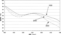
また、透過光の波長依存性が少ない特性、すなわち高透過率及びフラットな透過スペクトルとなる理由は現時点では不明であり、これらの効果は光学特性上経験的に得られた知見である。より詳細に説明するために、本発明の高屈折率層(a)4層と金属薄膜層(b)3層とを透明基体(A)上に交互に積層した透明導電性薄膜積層体の透過スペクトル図の例を図2に示す。100が(bH)の膜厚>(bL)の膜厚、200が(bH)の膜厚=(bL)の膜厚、300が(bH)の膜厚<(bL)の膜厚の場合の400nm〜700nmの透過スペクトルを示す。光線は、(bH)を入射側、(bL)側が透過側となる様に照射している。図2に示す如く、(bL)<(bH)となる透明導電性薄膜積層体においては、他の場合に比して透過率が高く、よりフラットな透過スペクトルを有することが分かる。 In addition, the reason why the wavelength dependence of transmitted light is small, that is, the reason for the high transmittance and the flat transmission spectrum is unknown at present, and these effects are findings obtained empirically from the viewpoint of optical characteristics. In order to explain in more detail, transmission of a transparent conductive thin film laminate in which four layers of high refractive index (a) and three metal thin film layers (b) of the present invention are alternately laminated on a transparent substrate (A). An example of a spectrum diagram is shown in FIG. 100 is the film thickness of (b H )> (b L ), 200 is the film thickness of (b H ) = (b L ), and 300 is the film thickness of (b H ) <(b L ) The transmission spectrum of 400 nm-700 nm in the case of the film thickness of is shown. The light beam is irradiated such that (b H ) is the incident side and the (b L ) side is the transmission side. As shown in FIG. 2, the transparent conductive thin film laminate satisfying (b L ) <(b H ) has a higher transmittance than other cases, and has a flatter transmission spectrum.
透明導電性薄膜積層体の光学特性として、一般的に、高い視感平均透過率を有することが好ましい。ここでいう好ましい視感平均透過率とは、50%以上であり、より好ましくは、60%以上、さらに好ましくは、70%以上である。 In general, the optical properties of the transparent conductive thin film laminate preferably have a high luminous average transmittance. The preferable luminous average transmittance here is 50% or more, more preferably 60% or more, and still more preferably 70% or more.
また、ディスプレイ用途として透明導電性薄膜積層体を用いる場合、高い視感平均透過率に加えて、可視光領域においてできるだけフラットな透過スペクトルを有する透明導電性薄膜積層体が適している。ここでいうフラットな透過スペクトルとしては、450nmの透過率T450を基準として、400〜500nmの透過率がT450±5%、550nmの透過率T550を基準として、500〜600nmの透過率がT550±5%、650nmの透過率T650を基準として、600〜700nmの透過率がT650±5%の範囲にあり、かつ、T550に対するT450、T650の比、すなわちT450/T550及びT650/T550の値がが0.90以上、特には0.95以上であることが好ましい。この様な特性を得るには、図2にも示したとおり金属層(bL)、金属層(bH)のうち、光線が入射する側の金属層を透過側のそれよりも厚くしておくことが好ましい。 Moreover, when using a transparent conductive thin film laminated body for a display use, in addition to a high luminous average transmittance, a transparent conductive thin film laminated body having a transmission spectrum that is as flat as possible in the visible light region is suitable. The flat transmission spectrum here is based on a transmittance T 450 of 450 nm, a transmittance of 400 to 500 nm is T 450 ± 5%, and a transmittance of 500 to 600 nm is based on a transmittance T 550 of 550 nm. T 550 ± 5%, 650 nm transmittance T 650 as a reference, the transmittance of 600-700 nm is in the range of T 650 ± 5%, and the ratio of T 450 to T 550 , T 650 , ie T 450 / The values of T 550 and T 650 / T 550 are preferably 0.90 or more, particularly 0.95 or more. In order to obtain such characteristics, as shown in FIG. 2, among the metal layer (b L ) and metal layer (b H ), the metal layer on the light incident side is made thicker than that on the transmission side. It is preferable to keep it.
上記の様な透過光線の波長依存性が少ない特性は、ディスプレイ用途などに本発明の透明導電性薄膜積層体を用いた場合、後述する色調調整の自由度が高くなり、用途に合わせた色調を実現するのに非常に有利である。 When the transparent conductive thin film laminate of the present invention is used for display applications and the like, the characteristics as described above having less wavelength dependency of transmitted light increase the degree of freedom of color tone adjustment to be described later. It is very advantageous to realize.
また、透明導電性薄膜積層体の電気特性としては、特にディスプレイ用途として用いられる場合、一般的に低い面抵抗を有していることが好ましい。ここでいう好ましい面抵抗とは、0.1Ω/□以上、15Ω/□以下、より好ましくは、0.1Ω/□以上、9Ω/□以下、さらに好ましくは、0.1Ω/□以上、7Ω/□以下である。 Moreover, as an electrical characteristic of a transparent conductive thin film laminated body, when using especially for a display use, it is generally preferable to have a low surface resistance. The preferable sheet resistance here is 0.1Ω / □ or more and 15Ω / □ or less, more preferably 0.1Ω / □ or more and 9Ω / □ or less, and further preferably 0.1Ω / □ or more, 7Ω / □ or less. □ Below.
本発明における実施例では、透明導電性薄膜積層体を7層(高屈折率層:4層、金属層:3層)で評価した。実際のPDPフィルターでは、5層、7層、9層、11層、13層として用いる為、条件を最適化することで高い視感平均透過率と低い面抵抗を有することができる。7層での好ましい視感平均透過率は50%以上であり、より好ましくは、60%以上、さらに好ましくは65%以上である。また、7層での好ましい面抵抗は、0.2Ω/□以上、10Ω/□以下、より好ましくは、0.2Ω/□以上、3Ω/□以下である。 In the examples of the present invention, the transparent conductive thin film laminate was evaluated with 7 layers (high refractive index layer: 4 layers, metal layer: 3 layers). Since an actual PDP filter is used as 5, 7, 9, 11, and 13 layers, it can have high luminous average transmittance and low surface resistance by optimizing the conditions. The preferable luminous average transmittance in the seven layers is 50% or more, more preferably 60% or more, and still more preferably 65% or more. Moreover, the preferable sheet resistance in 7 layers is 0.2Ω / □ or more and 10Ω / □ or less, and more preferably 0.2Ω / □ or more and 3Ω / □ or less.
本発明の透明導電性薄膜積層体は、透明電極他の公知の用途に用いることが出来るが、特にプラズマディスプレイパネル用光学フィルターに好適に用いることが出来る。その適用方法としては、公知のあらゆる方法を採用することができる。 The transparent conductive thin film laminate of the present invention can be used for known applications such as transparent electrodes, but can be suitably used particularly for an optical filter for a plasma display panel. As the application method, any known method can be adopted.
プラズマディスプレイパネル用光学フィルターの一般的な例としては、透明基体(A)上に高屈折率層(a)及び金属薄膜層(b)が形成された透明導電性薄膜積層体(B)と機能性透明層(C)と透明支持体(E)とが、(E)/(B)/(C)となるように透明粘着材層(D)で貼り合わせているものが挙げられる。この際、透明導電性薄膜積層体(B)の高屈折率層(a)、金属薄膜層(b)は、機能性透明層(C)側となるように配置されることが好ましい。なお、本発明はこれらの構成に限定されるものではない。 As a general example of an optical filter for a plasma display panel, a transparent conductive thin film laminate (B) in which a high refractive index layer (a) and a metal thin film layer (b) are formed on a transparent substrate (A) and a function The transparent transparent material layer (C) and the transparent support (E) are bonded together with the transparent adhesive layer (D) so as to be (E) / (B) / (C). At this time, it is preferable that the high refractive index layer (a) and the metal thin film layer (b) of the transparent conductive thin film laminate (B) are arranged on the functional transparent layer (C) side. The present invention is not limited to these configurations.
該機能性透明層(C)に付与される機能としては、具体的にハードコート性、反射防止性、防眩性、静電気防止性、防汚性、ガスバリア性、紫外線カット性、色調調整機能などの公知の性能、機能が挙げられるが、これに限定されるものではない。また、透明粘着材層(D)には、ディスプレイとしての色調を調整する機能を初めとする上記の機能を付与しても構わない。より具体的には、例えば特許3004222号公報等に記載の手法を好適に採用することが出来る。 Specific functions given to the functional transparent layer (C) include hard coat properties, antireflection properties, antiglare properties, antistatic properties, antifouling properties, gas barrier properties, ultraviolet ray cutting properties, color tone adjustment functions, etc. However, the present invention is not limited thereto. Moreover, you may provide said function including the function to adjust the color tone as a display to a transparent adhesive material layer (D). More specifically, for example, the method described in Japanese Patent No. 3004222 can be suitably employed.
本発明のプラズマディスプレイパネル用光学フィルターをプラズマディスプレイパネルの前面に配設することにより、電磁波遮断、近赤外線遮断の他、ディスプレイとして鮮明な画像を長期にわたって提供することが可能である。 By disposing the optical filter for a plasma display panel of the present invention on the front surface of the plasma display panel, it is possible to provide a clear image for a long period of time as a display in addition to blocking electromagnetic waves and blocking near infrared rays.
本発明の透明導電性薄膜積層体を実施例により具体的に説明する。なお、本発明は実施例によって限定を受けるものではない。また、比較例1及び2は、本発明の性能評価の比較品として作製した。 The transparent conductive thin film laminate of the present invention will be specifically described with reference to examples. In addition, this invention is not limited by the Example. Comparative examples 1 and 2 were produced as comparative products for performance evaluation of the present invention.
実施例1
(透明導電性薄膜積層体の作製)
ポリエチレンテレフタレート(PET)フィルム[厚さ75μm]上に、直流マグネトロンスパッタリング法を用いて下記の条件で高屈折率層と、金属薄膜層とを成膜した。
直流マグネトロンスパッタリング法を用いて、透明基体(A)上に、インジウムとセリウムと酸素からなる薄膜層(a)、銀とパラジウムと銅の合金薄膜層(bx、x=1,2,3)をA/a(厚さ:35nm)/b1(厚さ:8nm)/a(厚さ:75nm)/b2(厚さ:10nm)/a(厚さ:75nm)/b3(厚さ:9nm)/a(厚さ:35nm)なる順に積層し、透明導電性薄膜積層体を形成した。インジウムとセリウムと酸素からなる薄膜層は、高屈折率層(a)を、銀とパラジウムと銅との合金薄膜層は金属薄膜層(b)を構成する。インジウムとセリウムと酸素からなる薄膜層の形成には、ターゲットとして、酸化インジウム−酸化セリウム焼結体[In2O3:CeO2=80:20(質量比)]を用い、スパッタリングガスとしてアルゴン・酸素混合ガス[全圧:266mPa、酸素分圧8mPa]を用いた。また、銀とパラジウムと銅の合金薄膜層の形成には、ターゲットとして銀とパラジウムと銅の合金[Ag:Pd:Cu=98.0:1.0:1.0(原子数比)]を用い、スパッタリングガスとしてアルゴンガス[全圧:186mPa]を用いた。形成した透明導電性薄膜積層体の断面は図1と同様の構成である。
得られた透明導電性薄膜積層体は、高屈折率層側に易剥離性の保護フィルムを貼合して保管した。
Example 1
(Preparation of transparent conductive thin film laminate)
A high refractive index layer and a metal thin film layer were formed on a polyethylene terephthalate (PET) film [thickness: 75 μm] using a direct current magnetron sputtering method under the following conditions.
Using a direct current magnetron sputtering method, a thin film layer (a) made of indium, cerium and oxygen, an alloy thin film layer of silver, palladium and copper (b x , x = 1, 2, 3) on the transparent substrate (A) A / a (thickness: 35 nm) / b 1 (thickness: 8 nm) / a (thickness: 75 nm) / b 2 (thickness: 10 nm) / a (thickness: 75 nm) / b 3 (thickness) : 9 nm) / a (thickness: 35 nm) in this order to form a transparent conductive thin film laminate. The thin film layer made of indium, cerium and oxygen constitutes the high refractive index layer (a), and the alloy thin film layer of silver, palladium and copper constitutes the metal thin film layer (b). In forming a thin film layer composed of indium, cerium, and oxygen, an indium oxide-cerium oxide sintered body [In 2 O 3 : CeO 2 = 80: 20 (mass ratio)] is used as a target, and argon. An oxygen mixed gas [total pressure: 266 mPa, oxygen partial pressure 8 mPa] was used. In addition, an alloy thin film layer of silver, palladium and copper is formed by using an alloy of silver, palladium and copper [Ag: Pd: Cu = 98.0: 1.0: 1.0 (atomic ratio)] as a target. Argon gas [total pressure: 186 mPa] was used as the sputtering gas. The cross section of the formed transparent conductive thin film laminate is the same as that shown in FIG.
The obtained transparent conductive thin film laminate was stored with an easily peelable protective film bonded to the high refractive index layer side.
比較例1
インジウムとセリウムと酸素からなる薄膜層の代わりに、ターゲットとして酸化インジウム−酸化スズの焼結体[In2O3:SnO2=90:10(重量比)]を用いてインジウムとスズと酸素からなる薄膜層を形成し、かつ、銀とパラジウムと銅からなる合金薄膜層(b)の代わりに、ターゲットとして銀を用いて銀薄膜層を形成した以外は、実施例1と同様に実施した。形成した透明導電性薄膜積層体の断面は図1と同様の構成である。
Comparative Example 1
Instead of a thin film layer made of indium, cerium, and oxygen, an indium oxide-tin oxide sintered body [In 2 O 3 : SnO 2 = 90: 10 (weight ratio)] is used as a target from indium, tin, and oxygen. The thin film layer was formed, and instead of the alloy thin film layer (b) composed of silver, palladium, and copper, the silver thin film layer was formed using silver as a target. The cross section of the formed transparent conductive thin film laminate is the same as that shown in FIG.
比較例2
インジウムとセリウムと酸素からなる薄膜層の代わりに、ターゲットとして酸化インジウム−酸化スズの焼結体[In2O3:SnO2=90:10(重量比)]を用いてインジウムとスズと酸素からなる薄膜層を形成した以外は実施例1と同様に実施した。形成した透明導電性薄膜積層体の断面は図1と同様の構成である。
Comparative Example 2
Instead of a thin film layer made of indium, cerium, and oxygen, a sintered body of indium oxide-tin oxide [In 2 O 3 : SnO 2 = 90: 10 (weight ratio)] is used as a target from indium, tin, and oxygen. This was carried out in the same manner as in Example 1 except that a thin film layer was formed. The cross section of the formed transparent conductive thin film laminate is the same as that shown in FIG.
上記実施例1、比較例1及び2の透明導電性薄膜積層体の面抵抗、光線透過率の測定および塩化物イオンに対する以下の2種の塩化ナトリウム水溶液浸漬試験、塩化ナトリウム水溶液滴下試験を行った。 The following two types of sodium chloride aqueous solution immersion tests and sodium chloride aqueous solution dropping tests were conducted on the surface resistance and light transmittance of the transparent conductive thin film laminates of Example 1 and Comparative Examples 1 and 2 and chloride ions. .
(面抵抗)
上記の透明導電性薄膜積層体の保護フィルムを剥がし、四探針測定法(プローブ間隔1mm)により測定した。
(Surface resistance)
The protective film of said transparent conductive thin film laminated body was peeled, and it measured by the four probe measuring method (probe space | interval 1mm).
(光線透過率)
上記の透明導電性薄膜積層体の保護フィルムを剥がし、(株)日立製作所製分光光度計(U−3400)により可視領域の光線透過率を測定した。この際、光線が高屈折率層側から入射し、透明基体側に透過するように透明導電性薄膜積層体をセットし透過率T0の測定を行った。
(Light transmittance)
The protective film of the transparent conductive thin film laminate was peeled off, and the light transmittance in the visible region was measured with a spectrophotometer (U-3400) manufactured by Hitachi, Ltd. At this time, the transparent conductive thin film laminate was set so that light was incident from the high refractive index layer side and transmitted to the transparent substrate side, and the transmittance T 0 was measured.
(塩化ナトリウム水溶液浸漬試験)
上記の作成した透明導電性薄膜積層体の透明基体側を透明粘着材によりアクリル板(50mm×50mm×2mm)に貼り合わせる。次に保護フィルムを剥離して、0.5mol/lの塩化ナトリウム水溶液に9時間浸漬した場合と、21時間浸漬した場合の各浸漬時間における透過率(T0,T9、T21)及び面抵抗を測定し、T9/T0、T21/T0値で評価した。
(Sodium chloride aqueous solution immersion test)
The transparent substrate side of the transparent conductive thin film laminate produced above is bonded to an acrylic plate (50 mm × 50 mm × 2 mm) with a transparent adhesive material. Next, the protective film is peeled off, and the transmittance (T 0 , T 9 , T 21 ) and surface at each immersion time when immersed in a 0.5 mol / l sodium chloride aqueous solution for 9 hours and when immersed for 21 hours. Resistance was measured and evaluated by T 9 / T 0 and T 21 / T 0 values.
(塩化ナトリウム水溶液滴下試験)
まず、上記の透明導電性薄膜積層体の透明基体側を透明粘着材によりアクリル板(50mm×50mm×2mm)に貼り合わせる。保護フィルムを剥離して、直接0.001mol/lの塩化ナトリウム水溶液をマイクロシリンジにより1箇所につき0.1μlを10箇所滴下し、乾燥させた後、粘着材付きのPETフィルムを貼り合わせて評価サンプルとする。作製した評価サンプルは、環境劣化加速試験の条件である60℃、90%RHの恒温恒湿槽に10時間曝し、生じる点状欠陥のサイズを測定した。
上記のアクリル板や粘着材付きのPETフィルムを透明導電性薄膜積層体に貼り合わせる理由としては、評価するサンプルをより製品に近い構成にして評価する為である。
(Sodium chloride aqueous solution drop test)
First, the transparent substrate side of the transparent conductive thin film laminate is bonded to an acrylic plate (50 mm × 50 mm × 2 mm) with a transparent adhesive material. The protective film is peeled off, and 0.001 mol / l sodium chloride aqueous solution is directly dropped at 10 locations of 0.1 μl per location with a microsyringe and dried, and then a PET film with an adhesive material is attached to the evaluation sample. And The produced evaluation sample was exposed to a constant temperature and humidity chamber of 60 ° C. and 90% RH, which is the condition for the accelerated environmental degradation test, for 10 hours, and the size of the resulting point defects was measured.
The reason why the acrylic film and the PET film with an adhesive material are bonded to the transparent conductive thin film laminate is to make the sample to be evaluated closer to the product and evaluate.
実施例及び比較例の面抵抗、透過率および耐久性試験の評価結果を表1、表2に示した。 Tables 1 and 2 show the evaluation results of the sheet resistance, transmittance, and durability test of the examples and comparative examples.

表1より、実施例1の透明導電性薄膜積層体は、従来の銀層とITO層の積層体の例である比較例1と同等の面抵抗を有し、比較例1よりも高い透過率を有する透明導電性薄膜であり、非常にフラットな透過スペクトルを有する透明導電性薄膜積層体であることがわかる。また表2から実施例1の透明導電性薄膜積層体は、比較例1の積層体に比して大変優れた塩化物イオンに対する耐久性を有していることが分かる。 From Table 1, the transparent conductive thin film laminate of Example 1 has a sheet resistance equivalent to that of Comparative Example 1, which is an example of a conventional laminate of a silver layer and an ITO layer, and has a higher transmittance than Comparative Example 1. It can be seen that it is a transparent conductive thin film having a very flat transmission spectrum. Moreover, it turns out that the transparent conductive thin film laminated body of Example 1 has the durability with respect to the chloride ion very excellent compared with the laminated body of the comparative example 1 from Table 2.
また、一般的に塩化物イオンに対する耐久性が優れているとされている銀合金を用いた比較例2と比較しても、実施例1は、塩化物イオンに対する耐久性は同等レベル以上の耐久性を示している。また、光線透過率の波長依存性も少ない、すなわちフラットな透過スペクトルを示している。 Further, even when compared with Comparative Example 2 using a silver alloy which is generally considered to be excellent in durability against chloride ions, Example 1 has durability against chloride ions equal to or higher than that of Comparative Example 2. Showing sex. Further, the wavelength dependency of the light transmittance is small, that is, a flat transmission spectrum is shown.
つまり、本発明の透明導電性薄膜積層体は、面抵抗、透過率を維持したまま、塩化物イオンに対する耐久性が著しく向上した透明導電性薄膜積層体であり、かつ、可視光領域においてフラットな透過スペクトルを有する透明導電性薄膜積層体である。 That is, the transparent conductive thin-film laminate of the present invention is a transparent conductive thin-film laminate with significantly improved durability against chloride ions while maintaining sheet resistance and transmittance, and is flat in the visible light region. It is a transparent conductive thin film laminate having a transmission spectrum.
本発明は、プラズマディスプレイパネルに好適に用いることができ、高透過かつフラットな透過スペクトルを有していることから、より多彩な調色が可能であり、かつ、環境中の塩化物イオンによる銀の凝集による点状欠陥を著しく抑制した高耐久なプラズマディスプレイパネルを提供することが可能である。 INDUSTRIAL APPLICABILITY The present invention can be suitably used for a plasma display panel and has a high transmission and flat transmission spectrum, so that more various color adjustments are possible, and silver due to chloride ions in the environment. It is possible to provide a highly durable plasma display panel in which the point defects due to the aggregation of particles are remarkably suppressed.
100 金属薄膜層(bH)厚 > 金属薄膜層(bL)厚 の積層体の透過率曲線
200 金属薄膜層(bH)厚 = 金属薄膜層(bL)厚 の積層体の透過率曲線
300 金属薄膜層(bH)厚 < 金属薄膜層(bL)厚 の積層体の透過率曲線
10 透明基体
20 高屈折率層
30 金属薄膜層
100 Metal thin film layer (b H ) thickness> Metal thin film layer (b L ) thickness
Claims (6)
銀もしくは銀合金からなる金属薄膜層(b)とが、
両者の合計で5層〜13層繰り返して積層し、該金属薄膜層(b)の内、2つの主表面のそれぞれに最も近い金属薄膜層をそれぞれ(bL)、(bH)として
金属薄膜層(bL)の膜厚と金属薄膜層(bH)の膜厚とが異なることを特徴とする透明導電性薄膜積層体。 A high refractive index layer (a) comprising at least indium, cerium and oxygen;
A metal thin film layer (b) made of silver or a silver alloy,
A total of 5 to 13 layers are repeatedly laminated, and among the metal thin film layers (b), the metal thin film layers closest to the two main surfaces are defined as (b L ) and (b H ), respectively. A transparent conductive thin film laminate, wherein the thickness of the layer (b L ) is different from the thickness of the metal thin film layer (b H ).
Priority Applications (1)
| Application Number | Priority Date | Filing Date | Title |
|---|---|---|---|
| JP2004055546A JP2005242264A (en) | 2004-02-27 | 2004-02-27 | Transparent conductivity thin film laminated body and optical filter for plasma display panel using it |
Applications Claiming Priority (1)
| Application Number | Priority Date | Filing Date | Title |
|---|---|---|---|
| JP2004055546A JP2005242264A (en) | 2004-02-27 | 2004-02-27 | Transparent conductivity thin film laminated body and optical filter for plasma display panel using it |
Publications (2)
| Publication Number | Publication Date |
|---|---|
| JP2005242264A true JP2005242264A (en) | 2005-09-08 |
| JP2005242264A5 JP2005242264A5 (en) | 2006-07-27 |
Family
ID=35024028
Family Applications (1)
| Application Number | Title | Priority Date | Filing Date |
|---|---|---|---|
| JP2004055546A Withdrawn JP2005242264A (en) | 2004-02-27 | 2004-02-27 | Transparent conductivity thin film laminated body and optical filter for plasma display panel using it |
Country Status (1)
| Country | Link |
|---|---|
| JP (1) | JP2005242264A (en) |
Cited By (5)
| Publication number | Priority date | Publication date | Assignee | Title |
|---|---|---|---|---|
| WO2007046181A1 (en) * | 2005-10-19 | 2007-04-26 | Idemitsu Kosan Co., Ltd. | Semiconductor thin film and process for producing the same |
| JP2008221732A (en) * | 2007-03-15 | 2008-09-25 | Kiyoshi Chiba | Laminate |
| WO2011016387A1 (en) * | 2009-08-05 | 2011-02-10 | 住友金属鉱山株式会社 | Tablet for ion plating, method for producing same, and transparent conductive film |
| JP2011132556A (en) * | 2009-12-22 | 2011-07-07 | Sumitomo Metal Mining Co Ltd | Oxide evaporation material and high-refractive-index transparent film |
| DE112011100332T5 (en) | 2010-01-25 | 2012-11-22 | Sumitomo Metal Mining Company Limited | OXIDE EVAPORATIVE MATERIAL, STEAM-DIFFERENT THIN LAYER AND SOLAR CELL |
-
2004
- 2004-02-27 JP JP2004055546A patent/JP2005242264A/en not_active Withdrawn
Cited By (15)
| Publication number | Priority date | Publication date | Assignee | Title |
|---|---|---|---|---|
| US8062777B2 (en) | 2005-10-19 | 2011-11-22 | Idemitsu Kosan, Co., Ltd. | Semiconductor thin film and process for producing the same |
| CN101233257B (en) * | 2005-10-19 | 2010-09-22 | 出光兴产株式会社 | Semiconductor thin film and method for manufacturing the same |
| JP2007113048A (en) * | 2005-10-19 | 2007-05-10 | Idemitsu Kosan Co Ltd | Semi-conductor thin film and its manufacturing method |
| WO2007046181A1 (en) * | 2005-10-19 | 2007-04-26 | Idemitsu Kosan Co., Ltd. | Semiconductor thin film and process for producing the same |
| JP2008221732A (en) * | 2007-03-15 | 2008-09-25 | Kiyoshi Chiba | Laminate |
| EP2952493A3 (en) * | 2009-08-05 | 2016-01-20 | Sumitomo Metal Mining Co., Ltd. | Oxide sintered body, production method therefor, target, and transparent conductive film |
| WO2011016387A1 (en) * | 2009-08-05 | 2011-02-10 | 住友金属鉱山株式会社 | Tablet for ion plating, method for producing same, and transparent conductive film |
| CN102482154A (en) * | 2009-08-05 | 2012-05-30 | 住友金属矿山株式会社 | Tablet For Ion Plating, Method For Producing Same, And Transparent Conductive Film |
| US9721770B2 (en) | 2009-08-05 | 2017-08-01 | Sumitomo Metal Mining Co., Ltd. | Oxide sintered body, production method therefor, target, and transparent conductive film |
| US9005487B2 (en) | 2009-08-05 | 2015-04-14 | Sumitomo Metal Mining Co., Ltd. | Tablet for ion plating, production method therefor and transparent conductive film |
| JP5733208B2 (en) * | 2009-08-05 | 2015-06-10 | 住友金属鉱山株式会社 | Ion plating tablet, manufacturing method thereof, and transparent conductive film |
| JP2011132556A (en) * | 2009-12-22 | 2011-07-07 | Sumitomo Metal Mining Co Ltd | Oxide evaporation material and high-refractive-index transparent film |
| US8343387B2 (en) | 2009-12-22 | 2013-01-01 | Sumitomo Metal Mining Co., Ltd. | Oxide evaporation material and high-refractive-index transparent film |
| DE112011100332T5 (en) | 2010-01-25 | 2012-11-22 | Sumitomo Metal Mining Company Limited | OXIDE EVAPORATIVE MATERIAL, STEAM-DIFFERENT THIN LAYER AND SOLAR CELL |
| US8941002B2 (en) | 2010-01-25 | 2015-01-27 | Sumitomo Metal Mining Co., Ltd. | Oxide evaporation material, vapor-deposited thin film, and solar cell |
Similar Documents
| Publication | Publication Date | Title |
|---|---|---|
| EP1860930A1 (en) | Electromagnetic shielding laminate and display using same | |
| JP4961786B2 (en) | Transparent conductive film and transparent conductive film using the same | |
| US7740946B2 (en) | Electroconductive laminate, and electromagnetic wave shielding film for plasma display and protective plate for plasma display | |
| JP2010034577A (en) | Electromagnetic wave shielding laminate display employing the same | |
| JP6601199B2 (en) | Transparent conductor | |
| EP1918740A1 (en) | Laminated body for reflection film | |
| US20080174872A1 (en) | Electroconductive laminate, electromagnetic wave shielding film for plasma display and protective plate for plasma display | |
| KR20100057032A (en) | Conductive laminate | |
| JP2002313139A (en) | Transparent conductive thin film laminated body | |
| WO2003037056A1 (en) | Substrate with electromagnetic shield film | |
| JP2005242264A (en) | Transparent conductivity thin film laminated body and optical filter for plasma display panel using it | |
| JP2001052529A (en) | Transparent conductive thin film laminate | |
| JP2002371350A (en) | Method for manufacturing transparent laminate | |
| JP2004095240A (en) | Transparent electrode | |
| JP2003133787A (en) | Substrate with electromagnetic wave shielding film | |
| JP2003225964A (en) | Transparent conducting thin film laminate and its use application | |
| JP2004296140A (en) | Transparent conductive thin film laminate | |
| JP2000147245A (en) | Optical filter | |
| JP2005072255A (en) | Electromagnetic wave shielding sheet for plasma display and method of manufacturing the same | |
| JP2005116646A (en) | Transparent electromagnetic wave shielding film | |
| US20080174895A1 (en) | High reflection mirror and process for its production | |
| JP4820738B2 (en) | Electromagnetic wave shielding laminate and display device using the same | |
| JP3544878B2 (en) | Transparent conductive thin film laminate | |
| WO2021095550A1 (en) | Laminated structure | |
| JP2004047216A (en) | Transparent electrically conductive film |
Legal Events
| Date | Code | Title | Description |
|---|---|---|---|
| A521 | Written amendment |
Free format text: JAPANESE INTERMEDIATE CODE: A523 Effective date: 20060612 |
|
| A621 | Written request for application examination |
Free format text: JAPANESE INTERMEDIATE CODE: A621 Effective date: 20060612 |
|
| RD03 | Notification of appointment of power of attorney |
Free format text: JAPANESE INTERMEDIATE CODE: A7423 Effective date: 20080403 |
|
| A761 | Written withdrawal of application |
Free format text: JAPANESE INTERMEDIATE CODE: A761 Effective date: 20080716 |