JP2005129769A - Method for modifying semiconductor thin film, modified semiconductor thin film, method for evaluating the same, thin film transistor formed of semiconductor thin film, and image display device having circuit constituted by using the thin film transistor - Google Patents
Method for modifying semiconductor thin film, modified semiconductor thin film, method for evaluating the same, thin film transistor formed of semiconductor thin film, and image display device having circuit constituted by using the thin film transistor Download PDFInfo
- Publication number
- JP2005129769A JP2005129769A JP2003364539A JP2003364539A JP2005129769A JP 2005129769 A JP2005129769 A JP 2005129769A JP 2003364539 A JP2003364539 A JP 2003364539A JP 2003364539 A JP2003364539 A JP 2003364539A JP 2005129769 A JP2005129769 A JP 2005129769A
- Authority
- JP
- Japan
- Prior art keywords
- thin film
- semiconductor thin
- transmittance
- distribution
- polycrystalline semiconductor
- Prior art date
- Legal status (The legal status is an assumption and is not a legal conclusion. Google has not performed a legal analysis and makes no representation as to the accuracy of the status listed.)
- Pending
Links
- 239000010409 thin film Substances 0.000 title claims abstract description 199
- 239000004065 semiconductor Substances 0.000 title claims abstract description 188
- 238000000034 method Methods 0.000 title claims abstract description 139
- 238000009826 distribution Methods 0.000 claims abstract description 176
- 238000002834 transmittance Methods 0.000 claims abstract description 142
- 239000000758 substrate Substances 0.000 claims abstract description 81
- 239000010408 film Substances 0.000 claims abstract description 63
- 230000010363 phase shift Effects 0.000 claims abstract description 42
- 238000005224 laser annealing Methods 0.000 claims abstract description 37
- 230000003287 optical effect Effects 0.000 claims abstract description 31
- 230000003746 surface roughness Effects 0.000 claims abstract description 30
- 239000002344 surface layer Substances 0.000 claims abstract description 8
- 239000013078 crystal Substances 0.000 claims description 68
- 238000002425 crystallisation Methods 0.000 claims description 38
- 230000008025 crystallization Effects 0.000 claims description 35
- 238000011156 evaluation Methods 0.000 claims description 33
- 238000003384 imaging method Methods 0.000 claims description 14
- 230000008569 process Effects 0.000 claims description 11
- 230000001678 irradiating effect Effects 0.000 claims description 9
- 239000000155 melt Substances 0.000 claims description 2
- 238000002407 reforming Methods 0.000 claims 2
- 229910021417 amorphous silicon Inorganic materials 0.000 abstract description 37
- 238000007711 solidification Methods 0.000 abstract description 2
- 230000008023 solidification Effects 0.000 abstract description 2
- 229910021420 polycrystalline silicon Inorganic materials 0.000 description 56
- 239000002245 particle Substances 0.000 description 29
- 239000011295 pitch Substances 0.000 description 29
- XUIMIQQOPSSXEZ-UHFFFAOYSA-N Silicon Chemical compound [Si] XUIMIQQOPSSXEZ-UHFFFAOYSA-N 0.000 description 28
- 229910052710 silicon Inorganic materials 0.000 description 28
- 239000010703 silicon Substances 0.000 description 28
- 238000010586 diagram Methods 0.000 description 23
- 238000004519 manufacturing process Methods 0.000 description 17
- 239000010410 layer Substances 0.000 description 16
- 238000000137 annealing Methods 0.000 description 13
- 239000011521 glass Substances 0.000 description 11
- 230000035699 permeability Effects 0.000 description 11
- 239000004973 liquid crystal related substance Substances 0.000 description 10
- 238000007689 inspection Methods 0.000 description 9
- 238000002844 melting Methods 0.000 description 8
- 230000008018 melting Effects 0.000 description 8
- 230000000694 effects Effects 0.000 description 7
- 239000011248 coating agent Substances 0.000 description 6
- 238000000576 coating method Methods 0.000 description 6
- 238000012544 monitoring process Methods 0.000 description 6
- VYPSYNLAJGMNEJ-UHFFFAOYSA-N silicon dioxide Inorganic materials O=[Si]=O VYPSYNLAJGMNEJ-UHFFFAOYSA-N 0.000 description 6
- 238000010521 absorption reaction Methods 0.000 description 5
- 230000015572 biosynthetic process Effects 0.000 description 5
- 230000008859 change Effects 0.000 description 5
- 239000010453 quartz Substances 0.000 description 5
- 230000009467 reduction Effects 0.000 description 5
- 238000009434 installation Methods 0.000 description 4
- 238000005259 measurement Methods 0.000 description 4
- 238000002715 modification method Methods 0.000 description 4
- 229920005591 polysilicon Polymers 0.000 description 4
- 230000005540 biological transmission Effects 0.000 description 3
- 239000011159 matrix material Substances 0.000 description 3
- 230000010355 oscillation Effects 0.000 description 3
- 230000000737 periodic effect Effects 0.000 description 3
- 230000001737 promoting effect Effects 0.000 description 3
- 230000001681 protective effect Effects 0.000 description 3
- UFHFLCQGNIYNRP-UHFFFAOYSA-N Hydrogen Chemical compound [H][H] UFHFLCQGNIYNRP-UHFFFAOYSA-N 0.000 description 2
- BOTDANWDWHJENH-UHFFFAOYSA-N Tetraethyl orthosilicate Chemical compound CCO[Si](OCC)(OCC)OCC BOTDANWDWHJENH-UHFFFAOYSA-N 0.000 description 2
- 238000003491 array Methods 0.000 description 2
- 238000001918 dark-field optical micrograph Methods 0.000 description 2
- 230000005684 electric field Effects 0.000 description 2
- 229910052739 hydrogen Inorganic materials 0.000 description 2
- 239000001257 hydrogen Substances 0.000 description 2
- 239000011229 interlayer Substances 0.000 description 2
- 239000013081 microcrystal Substances 0.000 description 2
- 230000003252 repetitive effect Effects 0.000 description 2
- 238000011144 upstream manufacturing Methods 0.000 description 2
- 229910052581 Si3N4 Inorganic materials 0.000 description 1
- 229910000831 Steel Inorganic materials 0.000 description 1
- XAGFODPZIPBFFR-UHFFFAOYSA-N aluminium Chemical compound [Al] XAGFODPZIPBFFR-UHFFFAOYSA-N 0.000 description 1
- 229910052782 aluminium Inorganic materials 0.000 description 1
- 230000008901 benefit Effects 0.000 description 1
- 239000000969 carrier Substances 0.000 description 1
- 230000015556 catabolic process Effects 0.000 description 1
- 230000001364 causal effect Effects 0.000 description 1
- 238000007796 conventional method Methods 0.000 description 1
- 238000002109 crystal growth method Methods 0.000 description 1
- 230000003247 decreasing effect Effects 0.000 description 1
- 238000005516 engineering process Methods 0.000 description 1
- 230000001747 exhibiting effect Effects 0.000 description 1
- 238000002474 experimental method Methods 0.000 description 1
- 239000012535 impurity Substances 0.000 description 1
- 239000003550 marker Substances 0.000 description 1
- 230000004048 modification Effects 0.000 description 1
- 238000012986 modification Methods 0.000 description 1
- 229910021421 monocrystalline silicon Inorganic materials 0.000 description 1
- 238000001953 recrystallisation Methods 0.000 description 1
- 238000002310 reflectometry Methods 0.000 description 1
- 238000007493 shaping process Methods 0.000 description 1
- HQVNEWCFYHHQES-UHFFFAOYSA-N silicon nitride Chemical compound N12[Si]34N5[Si]62N3[Si]51N64 HQVNEWCFYHHQES-UHFFFAOYSA-N 0.000 description 1
- 229910052814 silicon oxide Inorganic materials 0.000 description 1
- 239000010959 steel Substances 0.000 description 1
Images


Classifications
-
- H—ELECTRICITY
- H01—ELECTRIC ELEMENTS
- H01L—SEMICONDUCTOR DEVICES NOT COVERED BY CLASS H10
- H01L21/00—Processes or apparatus adapted for the manufacture or treatment of semiconductor or solid state devices or of parts thereof
- H01L21/02—Manufacture or treatment of semiconductor devices or of parts thereof
- H01L21/04—Manufacture or treatment of semiconductor devices or of parts thereof the devices having at least one potential-jump barrier or surface barrier, e.g. PN junction, depletion layer or carrier concentration layer
- H01L21/18—Manufacture or treatment of semiconductor devices or of parts thereof the devices having at least one potential-jump barrier or surface barrier, e.g. PN junction, depletion layer or carrier concentration layer the devices having semiconductor bodies comprising elements of Group IV of the Periodic System or AIIIBV compounds with or without impurities, e.g. doping materials
- H01L21/20—Deposition of semiconductor materials on a substrate, e.g. epitaxial growth solid phase epitaxy
-
- B—PERFORMING OPERATIONS; TRANSPORTING
- B23—MACHINE TOOLS; METAL-WORKING NOT OTHERWISE PROVIDED FOR
- B23K—SOLDERING OR UNSOLDERING; WELDING; CLADDING OR PLATING BY SOLDERING OR WELDING; CUTTING BY APPLYING HEAT LOCALLY, e.g. FLAME CUTTING; WORKING BY LASER BEAM
- B23K26/00—Working by laser beam, e.g. welding, cutting or boring
- B23K26/02—Positioning or observing the workpiece, e.g. with respect to the point of impact; Aligning, aiming or focusing the laser beam
- B23K26/06—Shaping the laser beam, e.g. by masks or multi-focusing
- B23K26/064—Shaping the laser beam, e.g. by masks or multi-focusing by means of optical elements, e.g. lenses, mirrors or prisms
- B23K26/066—Shaping the laser beam, e.g. by masks or multi-focusing by means of optical elements, e.g. lenses, mirrors or prisms by using masks
-
- B—PERFORMING OPERATIONS; TRANSPORTING
- B23—MACHINE TOOLS; METAL-WORKING NOT OTHERWISE PROVIDED FOR
- B23K—SOLDERING OR UNSOLDERING; WELDING; CLADDING OR PLATING BY SOLDERING OR WELDING; CUTTING BY APPLYING HEAT LOCALLY, e.g. FLAME CUTTING; WORKING BY LASER BEAM
- B23K26/00—Working by laser beam, e.g. welding, cutting or boring
- B23K26/02—Positioning or observing the workpiece, e.g. with respect to the point of impact; Aligning, aiming or focusing the laser beam
- B23K26/06—Shaping the laser beam, e.g. by masks or multi-focusing
- B23K26/073—Shaping the laser spot
- B23K26/0738—Shaping the laser spot into a linear shape
-
- H—ELECTRICITY
- H01—ELECTRIC ELEMENTS
- H01L—SEMICONDUCTOR DEVICES NOT COVERED BY CLASS H10
- H01L21/00—Processes or apparatus adapted for the manufacture or treatment of semiconductor or solid state devices or of parts thereof
- H01L21/02—Manufacture or treatment of semiconductor devices or of parts thereof
- H01L21/02104—Forming layers
- H01L21/02365—Forming inorganic semiconducting materials on a substrate
- H01L21/02367—Substrates
- H01L21/0237—Materials
- H01L21/02422—Non-crystalline insulating materials, e.g. glass, polymers
-
- H—ELECTRICITY
- H01—ELECTRIC ELEMENTS
- H01L—SEMICONDUCTOR DEVICES NOT COVERED BY CLASS H10
- H01L21/00—Processes or apparatus adapted for the manufacture or treatment of semiconductor or solid state devices or of parts thereof
- H01L21/02—Manufacture or treatment of semiconductor devices or of parts thereof
- H01L21/02104—Forming layers
- H01L21/02365—Forming inorganic semiconducting materials on a substrate
- H01L21/02436—Intermediate layers between substrates and deposited layers
- H01L21/02439—Materials
- H01L21/02488—Insulating materials
-
- H—ELECTRICITY
- H01—ELECTRIC ELEMENTS
- H01L—SEMICONDUCTOR DEVICES NOT COVERED BY CLASS H10
- H01L21/00—Processes or apparatus adapted for the manufacture or treatment of semiconductor or solid state devices or of parts thereof
- H01L21/02—Manufacture or treatment of semiconductor devices or of parts thereof
- H01L21/02104—Forming layers
- H01L21/02365—Forming inorganic semiconducting materials on a substrate
- H01L21/02436—Intermediate layers between substrates and deposited layers
- H01L21/02494—Structure
- H01L21/02496—Layer structure
- H01L21/02502—Layer structure consisting of two layers
-
- H—ELECTRICITY
- H01—ELECTRIC ELEMENTS
- H01L—SEMICONDUCTOR DEVICES NOT COVERED BY CLASS H10
- H01L21/00—Processes or apparatus adapted for the manufacture or treatment of semiconductor or solid state devices or of parts thereof
- H01L21/02—Manufacture or treatment of semiconductor devices or of parts thereof
- H01L21/02104—Forming layers
- H01L21/02365—Forming inorganic semiconducting materials on a substrate
- H01L21/02518—Deposited layers
- H01L21/02521—Materials
- H01L21/02524—Group 14 semiconducting materials
- H01L21/02532—Silicon, silicon germanium, germanium
-
- H—ELECTRICITY
- H01—ELECTRIC ELEMENTS
- H01L—SEMICONDUCTOR DEVICES NOT COVERED BY CLASS H10
- H01L21/00—Processes or apparatus adapted for the manufacture or treatment of semiconductor or solid state devices or of parts thereof
- H01L21/02—Manufacture or treatment of semiconductor devices or of parts thereof
- H01L21/02104—Forming layers
- H01L21/02365—Forming inorganic semiconducting materials on a substrate
- H01L21/02656—Special treatments
- H01L21/02664—Aftertreatments
- H01L21/02667—Crystallisation or recrystallisation of non-monocrystalline semiconductor materials, e.g. regrowth
- H01L21/02675—Crystallisation or recrystallisation of non-monocrystalline semiconductor materials, e.g. regrowth using laser beams
- H01L21/02678—Beam shaping, e.g. using a mask
-
- H—ELECTRICITY
- H01—ELECTRIC ELEMENTS
- H01L—SEMICONDUCTOR DEVICES NOT COVERED BY CLASS H10
- H01L21/00—Processes or apparatus adapted for the manufacture or treatment of semiconductor or solid state devices or of parts thereof
- H01L21/02—Manufacture or treatment of semiconductor devices or of parts thereof
- H01L21/02104—Forming layers
- H01L21/02365—Forming inorganic semiconducting materials on a substrate
- H01L21/02656—Special treatments
- H01L21/02664—Aftertreatments
- H01L21/02667—Crystallisation or recrystallisation of non-monocrystalline semiconductor materials, e.g. regrowth
- H01L21/02675—Crystallisation or recrystallisation of non-monocrystalline semiconductor materials, e.g. regrowth using laser beams
- H01L21/02686—Pulsed laser beam
-
- H—ELECTRICITY
- H01—ELECTRIC ELEMENTS
- H01L—SEMICONDUCTOR DEVICES NOT COVERED BY CLASS H10
- H01L21/00—Processes or apparatus adapted for the manufacture or treatment of semiconductor or solid state devices or of parts thereof
- H01L21/02—Manufacture or treatment of semiconductor devices or of parts thereof
- H01L21/02104—Forming layers
- H01L21/02365—Forming inorganic semiconducting materials on a substrate
- H01L21/02656—Special treatments
- H01L21/02664—Aftertreatments
- H01L21/02667—Crystallisation or recrystallisation of non-monocrystalline semiconductor materials, e.g. regrowth
- H01L21/02691—Scanning of a beam
-
- H—ELECTRICITY
- H01—ELECTRIC ELEMENTS
- H01L—SEMICONDUCTOR DEVICES NOT COVERED BY CLASS H10
- H01L21/00—Processes or apparatus adapted for the manufacture or treatment of semiconductor or solid state devices or of parts thereof
- H01L21/02—Manufacture or treatment of semiconductor devices or of parts thereof
- H01L21/04—Manufacture or treatment of semiconductor devices or of parts thereof the devices having at least one potential-jump barrier or surface barrier, e.g. PN junction, depletion layer or carrier concentration layer
- H01L21/18—Manufacture or treatment of semiconductor devices or of parts thereof the devices having at least one potential-jump barrier or surface barrier, e.g. PN junction, depletion layer or carrier concentration layer the devices having semiconductor bodies comprising elements of Group IV of the Periodic System or AIIIBV compounds with or without impurities, e.g. doping materials
- H01L21/30—Treatment of semiconductor bodies using processes or apparatus not provided for in groups H01L21/20 - H01L21/26
- H01L21/324—Thermal treatment for modifying the properties of semiconductor bodies, e.g. annealing, sintering
-
- H—ELECTRICITY
- H01—ELECTRIC ELEMENTS
- H01L—SEMICONDUCTOR DEVICES NOT COVERED BY CLASS H10
- H01L27/00—Devices consisting of a plurality of semiconductor or other solid-state components formed in or on a common substrate
- H01L27/02—Devices consisting of a plurality of semiconductor or other solid-state components formed in or on a common substrate including semiconductor components specially adapted for rectifying, oscillating, amplifying or switching and having at least one potential-jump barrier or surface barrier; including integrated passive circuit elements with at least one potential-jump barrier or surface barrier
- H01L27/12—Devices consisting of a plurality of semiconductor or other solid-state components formed in or on a common substrate including semiconductor components specially adapted for rectifying, oscillating, amplifying or switching and having at least one potential-jump barrier or surface barrier; including integrated passive circuit elements with at least one potential-jump barrier or surface barrier the substrate being other than a semiconductor body, e.g. an insulating body
- H01L27/1214—Devices consisting of a plurality of semiconductor or other solid-state components formed in or on a common substrate including semiconductor components specially adapted for rectifying, oscillating, amplifying or switching and having at least one potential-jump barrier or surface barrier; including integrated passive circuit elements with at least one potential-jump barrier or surface barrier the substrate being other than a semiconductor body, e.g. an insulating body comprising a plurality of TFTs formed on a non-semiconducting substrate, e.g. driving circuits for AMLCDs
- H01L27/1259—Multistep manufacturing methods
- H01L27/127—Multistep manufacturing methods with a particular formation, treatment or patterning of the active layer specially adapted to the circuit arrangement
- H01L27/1274—Multistep manufacturing methods with a particular formation, treatment or patterning of the active layer specially adapted to the circuit arrangement using crystallisation of amorphous semiconductor or recrystallisation of crystalline semiconductor
- H01L27/1285—Multistep manufacturing methods with a particular formation, treatment or patterning of the active layer specially adapted to the circuit arrangement using crystallisation of amorphous semiconductor or recrystallisation of crystalline semiconductor using control of the annealing or irradiation parameters, e.g. using different scanning direction or intensity for different transistors
-
- H—ELECTRICITY
- H01—ELECTRIC ELEMENTS
- H01L—SEMICONDUCTOR DEVICES NOT COVERED BY CLASS H10
- H01L29/00—Semiconductor devices adapted for rectifying, amplifying, oscillating or switching, or capacitors or resistors with at least one potential-jump barrier or surface barrier, e.g. PN junction depletion layer or carrier concentration layer; Details of semiconductor bodies or of electrodes thereof ; Multistep manufacturing processes therefor
- H01L29/66—Types of semiconductor device ; Multistep manufacturing processes therefor
- H01L29/66007—Multistep manufacturing processes
- H01L29/66075—Multistep manufacturing processes of devices having semiconductor bodies comprising group 14 or group 13/15 materials
- H01L29/66227—Multistep manufacturing processes of devices having semiconductor bodies comprising group 14 or group 13/15 materials the devices being controllable only by the electric current supplied or the electric potential applied, to an electrode which does not carry the current to be rectified, amplified or switched, e.g. three-terminal devices
- H01L29/66409—Unipolar field-effect transistors
- H01L29/66477—Unipolar field-effect transistors with an insulated gate, i.e. MISFET
- H01L29/66742—Thin film unipolar transistors
- H01L29/6675—Amorphous silicon or polysilicon transistors
- H01L29/66757—Lateral single gate single channel transistors with non-inverted structure, i.e. the channel layer is formed before the gate
-
- H—ELECTRICITY
- H01—ELECTRIC ELEMENTS
- H01L—SEMICONDUCTOR DEVICES NOT COVERED BY CLASS H10
- H01L29/00—Semiconductor devices adapted for rectifying, amplifying, oscillating or switching, or capacitors or resistors with at least one potential-jump barrier or surface barrier, e.g. PN junction depletion layer or carrier concentration layer; Details of semiconductor bodies or of electrodes thereof ; Multistep manufacturing processes therefor
- H01L29/66—Types of semiconductor device ; Multistep manufacturing processes therefor
- H01L29/68—Types of semiconductor device ; Multistep manufacturing processes therefor controllable by only the electric current supplied, or only the electric potential applied, to an electrode which does not carry the current to be rectified, amplified or switched
- H01L29/76—Unipolar devices, e.g. field effect transistors
- H01L29/772—Field effect transistors
- H01L29/78—Field effect transistors with field effect produced by an insulated gate
- H01L29/786—Thin film transistors, i.e. transistors with a channel being at least partly a thin film
- H01L29/78651—Silicon transistors
- H01L29/7866—Non-monocrystalline silicon transistors
- H01L29/78672—Polycrystalline or microcrystalline silicon transistor
- H01L29/78675—Polycrystalline or microcrystalline silicon transistor with normal-type structure, e.g. with top gate
Abstract
Description
本発明は、非晶質半導体薄膜を多結晶半導体薄膜に改質するための半導体薄膜の改質方法および改質した半導体薄膜の評価方法、その半導体薄膜で形成した薄膜トランジスタ並びにこの薄膜トランジスタを用いて構成した回路を有するフラットパネル型の画像表示装置を含む半導体装置に好適なものである。 The present invention relates to a method for modifying a semiconductor thin film for modifying an amorphous semiconductor thin film into a polycrystalline semiconductor thin film, a method for evaluating the modified semiconductor thin film, a thin film transistor formed with the semiconductor thin film, and a configuration using the thin film transistor The present invention is suitable for a semiconductor device including a flat panel image display device having the above circuit.
例えば、液晶表示装置等のフラットパネル型の画像表示装置は、ガラスを好適とする絶縁基板(以下、単に基板とも称する)上に成膜した半導体薄膜に作り込んだ画素回路や駆動回路を有する。画素回路や駆動回路を構成する駆動素子としては薄膜トランジスタ(Thin Film Transistor:TFT)が多く用いられる。この薄膜トランジスタの活性層として、近年は非晶質半導体薄膜(典型的にはアモルファスシリコン半導体薄膜、あるいはa−Si膜とも称する)に代えて多結晶半導体薄膜(同じく典型的にはポリシリコン半導体薄膜、あるいはpoly−Si膜とも称する)を用いることで高精細で高画質の画像表示を得ることができる。 For example, a flat panel image display device such as a liquid crystal display device has a pixel circuit and a driver circuit formed in a semiconductor thin film formed on an insulating substrate (hereinafter also simply referred to as a substrate) made of glass. A thin film transistor (TFT) is often used as a driving element constituting a pixel circuit or a driving circuit. As an active layer of the thin film transistor, in recent years, a polycrystalline semiconductor thin film (also typically a polysilicon semiconductor thin film, also typically an amorphous silicon semiconductor thin film or a-Si film) is used instead of an amorphous semiconductor thin film (typically also referred to as an amorphous silicon semiconductor thin film or an a-Si film). Alternatively, a high-definition and high-quality image display can be obtained by using a poly-Si film).
薄膜トランジスタの活性層として用いる半導体薄膜をシリコン半導体薄膜を例として説明する。この活性層としての半導体薄膜を多結晶シリコン半導体薄膜とすることが非晶質シリコン半導体薄膜を用いることより優れた特性を得ることができる。その理由は、多結晶シリコン半導体薄膜は、非晶質シリコン半導体薄膜に比較してキャリア(nチャネルでは電子、pチャネルでは正孔)の移動度が高いことを挙げることができ、その結果、セルサイズ(画素サイズ)を小さくできることによる高精細化が可能となる。さらに、通常のポリシリコン半導体薄膜で形成した薄膜トランジスタの形成には、1000°C以上の高温プロセスが必要であるが、レーザ光によるシリコン層のみのアニールにより半導体薄膜を担持する基板が高温にならない低温ポリシリコン半導体薄膜形成技術では、安価なガラス基板の使用が可能な低温プロセスにおいて、移動度の高い薄膜トランジスタTFTの形成が可能となる。 A semiconductor thin film used as an active layer of a thin film transistor will be described by taking a silicon semiconductor thin film as an example. When the semiconductor thin film as the active layer is a polycrystalline silicon semiconductor thin film, it is possible to obtain characteristics superior to the use of the amorphous silicon semiconductor thin film. The reason is that the polycrystalline silicon semiconductor thin film has higher mobility of carriers (electrons in the n channel and holes in the p channel) than the amorphous silicon semiconductor thin film. High definition can be achieved by reducing the size (pixel size). Furthermore, the formation of a thin film transistor formed of a normal polysilicon semiconductor thin film requires a high-temperature process of 1000 ° C. or more, but the substrate carrying the semiconductor thin film is not heated to a high temperature by annealing only the silicon layer by laser light. In the polysilicon semiconductor thin film formation technology, a thin film transistor TFT having high mobility can be formed in a low temperature process in which an inexpensive glass substrate can be used.
通常、多結晶シリコン半導体薄膜の結晶の粒径が大きいほど移動度が高いので、大粒径の多結晶シリコン半導体薄膜を形成する方法としてさまざまな技術が提案されてきた。一般的には、「特許文献1」に示されるように、パルスレーザ光をラインビーム状に整形し、その強度分布のプロファイルを台形としてラインビームの短軸方向に短軸幅の約1/20程度のピッチで1ショット単位でずらしながら非晶質シリコン半導体薄膜にパルス照射の繰り返しを行う方法がとられる。非晶質シリコン半導体薄膜は照射されたレーザ光を吸収することによって温度が上昇し、溶けることで温度が低下する。このプロセスに伴ってシリコン半導体薄膜の結晶化が起こり、非晶質シリコン半導体薄膜は多結晶シリコン半導体薄膜へ変化する(ここで、これを改質と称する)。多結晶シリコン半導体薄膜の平均粒径は照射したレーザ光のエネルギ密度に依存して変化するが、非晶質シリコン半導体薄膜の結晶化に必要な最低エネルギ密度以上では、エネルギ密度を上げていくと粒径が大きくなるが、ある閾値以上では粒径が平均100nm(ナノメートル)以下の微結晶になる。そのため、この微結晶の閾値以下のエネルギ密度で照射を行わなければならない。
In general, the larger the crystal grain size of the polycrystalline silicon semiconductor thin film, the higher the mobility. Therefore, various techniques have been proposed as a method for forming a polycrystalline silicon semiconductor thin film having a large grain size. In general, as shown in “
これに対して「特許文献2」では、パルスレーザの照射領域の強度分布のプロファイルを台形として、最大強度を非晶質シリコン半導体薄膜が微結晶の多結晶シリコン半導体薄膜に変化する閾値以上の値を有する強度分布プロファイルとして、当該プロファイルの裾の強度分布で大粒径化する方法を開示している。
On the other hand, in “
以上は、平均粒径が1μm(ミクロンメートル)程度の技術であり、例えば膜厚50nmの非晶質シリコン半導体薄膜を多結晶シリコン半導体薄膜に変化する場合に0.3μm以上の粒径となるレーザエネルギ密度のマージンは、約10%程度であるが、そのうち半分程度は突起のPV値が70nm以上になる。なお、PV値とは測定範囲内の最高値と最低値との差で定義される。 The above is a technique with an average particle size of about 1 μm (micron meter). For example, a laser having a particle size of 0.3 μm or more when an amorphous silicon semiconductor thin film having a thickness of 50 nm is changed to a polycrystalline silicon semiconductor thin film. The energy density margin is about 10%, of which about half of the PV value of the protrusion is 70 nm or more. The PV value is defined as the difference between the highest value and the lowest value within the measurement range.
シリコン半導体薄膜の大粒径化技術の別の方法として、光強度分布を制御する方法がある。この従来技術の一つとしては、「特許文献3」に開示されている様に、逐次的横方向結晶成長法(SLS法)と呼ばれる方法がある。この方法は、面内方向にレーザ光の強度分布をミクロンメートルのサイズの複数のビーム素片に細切れにすることにより面内方向に温度勾配を形成し、強制的に横方向の結晶成長を促す方法である。この方法では、複数の結晶粒の結晶成長の向きがお互いにぶつかり会う境界において表面に突起が形成される。 Another method for increasing the grain size of a silicon semiconductor thin film is to control the light intensity distribution. As one of the prior arts, there is a method called sequential lateral crystal growth method (SLS method) as disclosed in “Patent Document 3”. This method divides the intensity distribution of laser light in the in-plane direction into a plurality of beam pieces having a size of micrometer, thereby forming a temperature gradient in the in-plane direction and forcibly promoting lateral crystal growth. Is the method. In this method, protrusions are formed on the surface at boundaries where crystal growth directions of a plurality of crystal grains collide with each other.
この突起が形成される位置は、各ビーム素片の光強度のピーク位置に対応する。なぜならば、この位置が最も温度が高くなるので当該ピーク位置の両側から結晶化が該ピーク位置に向かって進行し、ピーク位置において結晶成長がぶつかるからである。この突起は前述の台形プロファイルのラインビーム整形したレーザ光照射による多結晶シリコン半導体薄膜の突起より高く、PV値で100nm以上になる場合がある。 The position where this protrusion is formed corresponds to the peak position of the light intensity of each beam segment. This is because the temperature is highest at this position, so that crystallization proceeds from both sides of the peak position toward the peak position, and crystal growth collides at the peak position. This protrusion is higher than the protrusion of the polycrystalline silicon semiconductor thin film formed by laser beam irradiation with the above-mentioned trapezoidal profile line beam, and may have a PV value of 100 nm or more.
「特許文献4」と「特許文献7」で提案された方法は、「特許文献2」に開示される方法の改良技術であり、レーザ光を最初に高強度のエネルギで照射した後、それよりも低い強度のエネルギで照射する強度分布制御により結晶化することで結晶粒を大きくする方法である。この分布制御の方法については、焦点位置と基板表面との位置を変化させることで非対称的な強度分布が得られるとしている。但し、この方法により非対称的な分布形状の変化が得られる因果関係は開示されていない。これに対して、「特許文献5」では同様に焦点位置と基板表面との位置を変化させることで、台形形状から逆釣鐘形状になるとしており、「特許文献4」の結果と矛盾する。「特許文献6」にも、同様の照射分布で大粒径の結晶が得られるとしているが、レーザ光のビーム形成方法に関する記述はない。
The method proposed in “
上記した従来技術は、レーザ光としてパルスレーザを用いたものである。この様なパルスレーザを用いたシリコン半導体薄膜の結晶化方法すなわち、ここで言う改質方法では、結晶化後の多結晶シリコン半導体薄膜の表面に突起が形成されるため、その表面凹凸が大きい。そのため、この半導体薄膜に例えば薄膜トランジスタを作り込む場合には、多結晶シリコン半導体薄膜上に形成するゲート絶縁膜を厚くする必要がある。その結果、ゲート絶縁膜の膜厚に反比例してトランジスタのオン電流が小さくなるという問題がある。 The above-described conventional technique uses a pulse laser as the laser light. In such a crystallization method of a silicon semiconductor thin film using a pulse laser, that is, the modification method referred to here, since the protrusion is formed on the surface of the polycrystalline silicon semiconductor thin film after crystallization, the surface unevenness is large. Therefore, for example, when a thin film transistor is formed in this semiconductor thin film, it is necessary to increase the thickness of the gate insulating film formed on the polycrystalline silicon semiconductor thin film. As a result, there is a problem that the on-state current of the transistor is reduced in inverse proportion to the thickness of the gate insulating film.
台形プロファイルとしたレーザ光のラインビーム照射で形成された多結晶シリコン薄膜の突起を低減するための改良された方法として、レーザアニールを複数回行い、それぞれ異なるエネルギ密度で照射する方法によって、突起を低減する方法が「特許文献8」に開示されている。特許文献8に開示された内容は次のとおりである。すなわち、非晶質シリコン半導体薄膜の成膜時に含まれる水素がレーザアニールによって急激に放出されて膜表面が荒れる。このとき、結晶化が起こる閾値値以下の低エネルギ密度のレーザ光を照射し、結晶化アニールの前に水素を放出させることによって膜表面のあれを防止するというものである。
As an improved method for reducing protrusions on polycrystalline silicon thin films formed by laser beam line beam irradiation with a trapezoidal profile, laser annealing is performed multiple times, and irradiation is performed at different energy densities. A reduction method is disclosed in “
また、SLS法における突起低減方法として、レーザ光照射で結晶化アニールを行った後に完全溶融のエネルギ密度の25%から75%の値で2回目にレーザ光照射することにより、突起を低減する方法が「特許文献9」に開示されている。
Further, as a method of reducing protrusions in the SLS method, a method of reducing protrusions by performing laser light irradiation at a value of 25% to 75% of the energy density of complete melting after performing crystallization annealing by laser light irradiation. Is disclosed in “
しかし、以上の方法には以下のような欠点がある。すなわち、レーザ光を多段で照射するため、基板上を何回もレーザ光を走査する必要があり、アニール工程に要する時間が長くなるという欠点がある。さらに、複数のエネルギ密度をそれぞれ異なる照射時間で複数走査で行う場合は、パルスレーザの繰り返し周波数が一定であるために照射時間の相違は走査速度を変えることになり、半導体薄膜を成膜した基板上における各走査のレーザ光の照射パルスを重ねた場合、突起低減効果が基板上でまだらになるという欠点がある。 However, the above method has the following drawbacks. That is, since the laser beam is irradiated in multiple stages, it is necessary to scan the laser beam several times over the substrate, and there is a disadvantage that the time required for the annealing process becomes long. Furthermore, when performing multiple scans with multiple energy densities at different irradiation times, the repetition rate of the pulse laser is constant, so the difference in irradiation time changes the scanning speed, and the substrate on which the semiconductor thin film is formed When the irradiation pulse of the laser beam of each scan above is overlapped, there is a drawback that the protrusion reduction effect is mottled on the substrate.
突起低減が効果的な方法を用いて多結晶シリコン半導体薄膜を形成しても、レーザ出力の時間変動や結晶化前の非晶質シリコン薄膜厚の面内変動が存在するために、結晶化後に突起の検査を行い、突起が高い領域、言い換えれば表面ラフネスが大きい領域を検出して、その領域を再度結晶化するなどの工程を含めなければ、基板全面で管理基準以下の表面ラフネスとすることができない。このような表面ラフネスを計測する公知技術としては、原子間力顕微鏡による評価方法がある。しかし、この方法では10μm×10μmの微小領域を評価するのに少なくとも数分程度を要するので、基板全面の表面ラフネスを評価することは時間的に不可能である。 Even if a polycrystalline silicon semiconductor thin film is formed using a method that is effective in reducing protrusions, there is time variation of laser output and in-plane variation of amorphous silicon thin film thickness before crystallization. Inspect the protrusions, detect areas with high protrusions, in other words, detect areas with high surface roughness, and if they do not include processes such as recrystallization, the surface roughness should be below the control standard on the entire substrate. I can't. As a known technique for measuring such surface roughness, there is an evaluation method using an atomic force microscope. However, this method requires at least several minutes to evaluate a micro area of 10 μm × 10 μm, and therefore it is impossible to evaluate the surface roughness of the entire surface of the substrate.
この表面ラフネスを高速に評価する方法としては表面光沢度(反射率)で評価する方法が「特許文献10」に示されている。この方法は、反射率で評価するので多結晶シリコン半導体薄膜の厚さやガラス基板と多結晶シリコン半導体薄膜の間の下地膜の厚さによる干渉の影響が存在するという欠点がある。多結晶シリコン半導体薄膜の粒径の面内分布を高速に評価する方法に関しては、「特許文献11」に開示されているように、散乱光の角度分布の広がり幅で粒径を計測する方法が知られている。
非晶質シリコン半導体薄膜をレーザアニールして結晶化した多結晶シリコン半導体薄膜の表面に形成される突起を低減するために、非晶質シリコン半導体薄膜を複数のエネルギ密度のレーザ光で照射する方法では、照射するレーザ光のエネルギ密度ごとに走査回数が多くなり、結晶化工程の時間が長くなるという欠点がある。さらに、走査ピッチの異なる複数の走査の重ね合わせによる突起低減効果が、基板上(ガラス等の基板に成膜された半導体薄膜上、以下同じ)でまだらになるという欠点がある。このことを図を用いて説明する。 A method of irradiating an amorphous silicon semiconductor thin film with laser beams having a plurality of energy densities in order to reduce protrusions formed on the surface of the polycrystalline silicon semiconductor thin film obtained by crystallizing the amorphous silicon semiconductor thin film by laser annealing. However, there is a drawback that the number of scans increases for each energy density of the laser beam to be irradiated, and the time for the crystallization process becomes longer. Furthermore, there is a drawback that the effect of reducing protrusions by overlapping a plurality of scans having different scan pitches is mottled on a substrate (the same applies hereinafter on a semiconductor thin film formed on a substrate such as glass). This will be described with reference to the drawings.
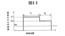
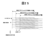
図22はレーザ光照射エネルギ密度の時間変化の説明図である。図22の縦軸におけるEthは結晶化が起こる下限の閾値を示す。また、図23は図22の時間変化を複数のレーザ光走査で実施する場合に起こる副作用の説明図であり、実線はレーザ光の照射エネルギ密度E1の走査ピッチ、破線はレーザ光の照射エネルギ密度E2の走査ピッチを示す。ここでは、図22に示す様に、基板の同一箇所を1回目のエネルギ密度をE1、時間T1の間で照射し、2回目のエネルギ密度はE2、時間T2の間で照射する条件で基板全体を走査しながらレーザ光を照射する場合を考える。パルスレーザの繰り返し周波数は一定であるので、1回目の走査のピッチは1/T1に比例した値(∝1/T1)であり、2回目の走査ピッチは1/T2に比例した値(∝1/T2)となる。そうすると、上記2種類の走査ピッチの重ね合わせを考えたとき、図23に示した様に基板上での重ね合わせがまだら状に不均一になる。この影響によって、突起の平均高さはまだら状に面内変動した分布となる。 FIG. 22 is an explanatory diagram of the change over time of the laser beam irradiation energy density. Eth on the vertical axis in FIG. 22 represents a lower limit threshold value at which crystallization occurs. FIG. 23 is an explanatory diagram of side effects that occur when the time change of FIG. 22 is performed by a plurality of laser beam scans, the solid line is the scan pitch of the laser beam irradiation energy density E1, and the broken line is the laser beam irradiation energy density. The scanning pitch of E2 is shown. Here, as shown in FIG. 22, the same portion of the substrate is irradiated with the first energy density during E1 and time T1, and the second energy density is irradiated during E2 and time T2. Consider the case of irradiating laser light while scanning. Since the repetition frequency of the pulse laser is constant, the pitch of the first scan is a value proportional to 1 / T1 (∝1 / T1), and the second scan pitch is a value proportional to 1 / T2 (∝1 / T2). Then, when considering the superposition of the above two types of scanning pitches, the superposition on the substrate becomes uneven in a mottled manner as shown in FIG. Due to this influence, the average height of the projections becomes a distribution that varies in a mottled manner in the plane.
したがって、このような周期的な突起の高い領域の発生が無い突起低減方法およびそれを可能とするレーザアニール方法を用いた半導体薄膜の製造方法およびその製造装置を提供することが本発明の第1の目的である。また、本発明の製造方法で製造した半導体薄膜を提供することが本発明の第2の目的である。 Accordingly, it is a first aspect of the present invention to provide a method for manufacturing a semiconductor thin film using a method for reducing protrusions that does not generate such a high region of periodic protrusions, a laser annealing method that enables the method, and a manufacturing apparatus therefor. Is the purpose. It is a second object of the present invention to provide a semiconductor thin film manufactured by the manufacturing method of the present invention.
さらに、大粒径化でかつ突起を低減する方法で結晶化を行ったとしても、レーザ出力の時間変動や非晶質シリコン半導体薄膜厚の基板面内変動によって、粒径および突起の高さが管理基準以内で形成されているとは限らない。したがって、基板全面で粒径の他に突起の高さの全数検査が可能な計測方法で製造した半導体薄膜の特性を評価する評価方法及びその評価装置を提供することが本発明の第3の目的である。 Furthermore, even if crystallization is performed by increasing the grain size and reducing the protrusions, the grain size and the height of the protrusions may vary depending on the time variation of the laser output and the in-plane variation of the amorphous silicon semiconductor thin film thickness. It is not necessarily formed within the management standards. Therefore, it is a third object of the present invention to provide an evaluation method and an evaluation apparatus for evaluating the characteristics of a semiconductor thin film manufactured by a measuring method capable of inspecting the total height of the protrusions in addition to the particle diameter over the entire surface of the substrate. It is.
そして、本発明の半導体薄膜で形成した薄膜トランジスタを提供することが本発明の第4の目的である。そして、この薄膜トランジスタを用いて構成した回路を備えた画像表示装置を提供することが本発明の第5の目的である。 It is a fourth object of the present invention to provide a thin film transistor formed of the semiconductor thin film of the present invention. It is a fifth object of the present invention to provide an image display device provided with a circuit configured using this thin film transistor.
本発明の半導体薄膜の製造方法は、レーザ光の照射による溶融と凝固を行う、所謂レーザアニール手法を用いて非晶質シリコン半導体薄膜を多結晶シリコン半導体薄膜化するにあたり、多結晶化したシリコン半導体薄膜の表面ラフネスを低減するために多段のエネルギ密度照射でアニールする方法である。このアニールする方法では、レーザ光透過率の面内分布を制御した透過率分布フィルタを照射光学系に設置し、レーザ光を走査方向と直交する方向に長軸方向を有するラインビームに整形する。そして、ラインビームに整形したレーザ光の走査方向である該ラインビームの短軸方向の光強度分布を制御することで、走査方向において複数のエネルギ密度による照射を1回の走査で行うことを主要な特徴とする。 The method for producing a semiconductor thin film according to the present invention is a method for forming a polycrystalline silicon semiconductor thin film by converting the amorphous silicon semiconductor thin film into a polycrystalline silicon semiconductor thin film by using a so-called laser annealing method in which melting and solidification are performed by laser light irradiation. In order to reduce the surface roughness of the thin film, it is a method of annealing by multi-stage energy density irradiation. In this annealing method, a transmittance distribution filter in which the in-plane distribution of laser light transmittance is controlled is installed in the irradiation optical system, and the laser light is shaped into a line beam having a major axis direction perpendicular to the scanning direction. Then, by controlling the light intensity distribution in the minor axis direction of the line beam, which is the scanning direction of the laser beam shaped into a line beam, it is mainly performed to perform irradiation with a plurality of energy densities in one scanning. Features.
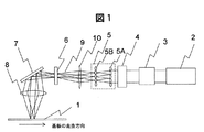
本発明による半導体薄膜の改質方法と、改質した半導体薄膜の評価方法の特徴を、後述する実施例の説明にも用いる各図を参照して説明する。なお、ここでの説明と後述する実施例での説明とが重複する箇所もあることを予め明示しておく。図1は本発明による半導体薄膜の製造方法を実現するためのレーザアニール光学系である。図1に示したレーザアニール装置の光学系は、短軸ホモジナイザ5と長軸ホモジナイザ4によって、強度が均一なラインビーム分布を形成している。短軸ホモジナイザ5は対向する一組のシリンドリカルレンズアレイ5Aと5Bで構成される。この短軸ホモジナイザ5にはレーザ光源2からのレーザ光をアッテネータ3および長軸ホモジナイザ4を透過して入射させる。アッテネータ3はレーザ光源2から発生したレーザビームが所定のエネルギを有するように調節するためのものである。
The characteristics of the method for modifying a semiconductor thin film and the method for evaluating the modified semiconductor thin film according to the present invention will be described with reference to the drawings used for the description of the embodiments described later. In addition, it is clearly shown in advance that there is a place where the explanation here and the explanation in the embodiments described later overlap. FIG. 1 shows a laser annealing optical system for realizing a method of manufacturing a semiconductor thin film according to the present invention. The optical system of the laser annealing apparatus shown in FIG. 1 forms a line beam distribution with uniform intensity by the
短軸ホモジナイザ5より後に設置されたレンズ10によって短軸ホモジナイザ5内のシリンドリカルレンズアレイ5Aと5Bの各レンズ素子を透過したレーザ光9が一次結像面で重ね合わされる。この1次結像面に重ね合わされるのは、短軸ホモジナイザ5の前段のシリンドリカルレンズアレイ5Aの各レンズ素子内部の光強度分布である。シリンドリカルレンズアレイ5Aの各レンズ素子が小さく、数が多いほど一次結像面における光強度分布が均一になる。
この一次結像面の位置に透過率の面内分布を形成したフィルタ(透過率分布フィルタ)6を設置する。この透過率分布フィルタ6は透明石英製であり、図2に示す様に表面に反射率コーティングを施すことによって、透過率の面内分布を±0.5%程度の精度で制御したフィルタとなっている。なお、透過率分布フィルタ6の詳細構成は実施例の項で説明する。一次結像面の光強度分布は、このフィルタの透過率分布によって±0.5%程度の精度で制御され、この光強度分布を有するレーザ光が、ミラー7とレンズ8によって半導体薄膜が成膜された基板1の表面に縮小投影される。以上の短軸分布制御法を一次結像面制御方法と呼ぶことにする。
A filter (transmittance distribution filter) 6 in which an in-plane distribution of transmittance is formed is installed at the position of the primary imaging plane. The
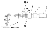
次に、短軸方向の強度分布を制御する別の方法を、図5および図6を参照して説明する。短軸方向の強度分布を制御する別の方法は、短軸ホモジナイザ5の前段で、該短軸ホモジナイザ5を構成するシリンドリカルレンズアレイ5Aの各レンズ素子内部の光強度分布を透過率分布フィルタ16で制御することで、合成された分布の形状を制御するようにしたものである。図5に示す様に、透過率分布フィルタ16は短軸ホモジナイザ5の直前に設置する。この場合の透過率分布フィルタ16は、図6に示す様に、その透過率分布がシリンドリカルレンズアレイ5Aに対応して反射率制御コーティング膜をストライプ状に形成して、各レンズ素子の短軸方向の光強度分布を制御する様に設置する。最終的に、基板1の表面上での光強度分布形状は各レンズ素子内の強度分布の重ね合わせの分布になる。図6はレンズ素子3個分のストライプを示している。この方法をホモジナイザ素子内分布制御方法と呼ぶことにする。なお、透過率分布フィルタ16の詳細構成は実施例の項で説明する。
Next, another method for controlling the intensity distribution in the minor axis direction will be described with reference to FIGS. Another method for controlling the intensity distribution in the short axis direction is a stage before the
上記した2種類の短軸分布制御方法は、レーザ光をラインビーム形状に整形するレーザアニール装置における光学系および結晶化方法の改良であるが、ラインビームではないレーザアニール方法にも適用可能である。以下に特許文献1に開示されているようなSLS法への本発明の適用方法を説明する。
The two types of short axis distribution control methods described above are improvements in the optical system and crystallization method in a laser annealing apparatus that shapes laser light into a line beam shape, but are also applicable to laser annealing methods that are not line beams. . A method for applying the present invention to the SLS method as disclosed in
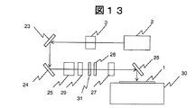
一般的なSLS結晶化装置は、図13に示したように、光源2とアッテネータ3、ホモジナイザ25、レンズ29、マスク26、イメージングレンズ27、そして非晶質シリコン半導体薄膜を成膜した基板1が置かれる移動ステージ30から構成される。アッテネータ3とホモジナイザ25間、及びイメージングレンズ27と移動ステージ30間には入射したレーザ光を所定の角度で反射してレーザ光の方向を変化させるためのミラー23、24、28が各々配置される。ホモジナイザ25はレーザ光のビーム整形と整形したレーザビーム内光強度を均一にするための光学系であり、レンズ29との組み合わせによってマスク26の位置に均一なビーム内強度分布を形成するようにしてある。
As shown in FIG. 13, a general SLS crystallization apparatus includes a
このマスク26の位置は、図1に示した光学系の一次結像面に対応する。このマスク26によって、基板1の表面上に光強度の明暗のパターンを形成し、面内方向に温度勾配を形成することで、横方向(走査方向と直交する方向、幅方向)への結晶成長を促して大粒径の結晶を形成する方法である。本発明の透過率面内分布制御フィルタすなわち透過率分布フィルタ31は、下記の図14で説明するように、マスク26の近傍に設置することによって、当該マスク内の各パターンを透過する光強度を制御する。
The position of the
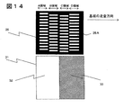
図14に図13におけるマスクパターンとフィルタ透過率パターンとの組み合わせの一例を示す。マスクの開口部すなわちスリット26Aは基板1の走査方向に長軸を有する。マスクパターンの構成は次のとおりである。A領域とB領域はお互いに走査方向に対してスリット26Aの間隔の配列周期の位相が1/2周期だけずらされ、同様にC領域とD領域も互いに位相を走査方向に対して1/2周期だけずらし、且つA領域とC領域との周期位相のずれを互いに1/2周期とは異なる様に例えば1/4周期の様に設定する。この様に設定する理由は、非晶質シリコン半導体薄膜を多結晶シリコン半導体薄膜に改質したときのA領域とB領域のパターンの照射によって形成される突起の位置と、C領域とD領域のパターンの照射によって形成される突起の位置とを相対的にずらすためである。
FIG. 14 shows an example of a combination of the mask pattern and the filter transmittance pattern in FIG. The opening of the mask, that is, the
上記マスク26に対応する透過率分布フィルタ31は、反射防止膜を形成した領域32と反射膜を形成した領域33の透過率の差が10%以上有する。この透過率分布フィルタ31をマスク26の近傍に設置する。設置場所は、マスク26の設置位置より上流側でも下流側でも良い。パルスレーザの繰り返し発振周波数に対して走査ピッチを調整し、マスクパターンの各領域が1ショットだけ照射されるようにする。1回の走査の中の照射の過程を図15を参照して説明する。図15(a)の基板上に成膜した非晶質シリコン膜1AにA領域のパターンが1ショットだけ照射されると、照射されていない領域が残る。この照射されていない領域はA領域のマスクされている部分に対応しており、結晶化していない部分である。
The
図15(b)のように、結晶化した領域であるA領域には、2つの横方向に成長した結晶粒36と37が、突起35が形成された粒界を挟んで存在する形状となる。次のショット時はB領域のパターンが同一エネルギ密度で1ショット照射される(図15(c))。このショットにより先のショットで結晶化していなかった領域は、両側の結晶を種にして結晶が中心に向かって成長する。この結果、突起間距離が平均粒界サイズとなる多結晶シリコン半導体薄膜が形成される。この後、図15(d)に示したC領域パターン、図15(e)に示したD領域パターンが10%以上低いエネルギのレーザ光で照射される。
As shown in FIG. 15B, in the A region, which is a crystallized region, two laterally grown
この場合、突起が形成される位置が異なる様に10%以上低いエネルギ密度で照射される。このエネルギ密度のレーザ光では、シリコン半導体薄膜の厚さ方向全体を溶融することが不可能であり、シリコン半導体薄膜の表層のみ溶融されるので、粒界を形成することができず、シリコン半導体薄膜の表層に突起のみが形成される。この結果、図15(d)のように粒界位置ではない場所に低い突起40が形成される。もともと高い突起は低い突起の形成のためにシリコン半導体薄膜が移動するために、B領域照射後まで形成されていた突起39の高さは低くなる。以上の様に、本発明は突起を低減するために多段のエネルギ密度によるSLS法を1回の走査で行うことを特徴とするものである。
In this case, irradiation is performed with an energy density of 10% or lower so that the positions where the protrusions are formed are different. With this energy density laser light, it is impossible to melt the entire thickness direction of the silicon semiconductor thin film, and only the surface layer of the silicon semiconductor thin film is melted, so that a grain boundary cannot be formed. Only the protrusions are formed on the surface layer. As a result, as shown in FIG. 15 (d), a
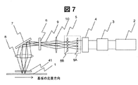
さらに、上記SLS法とは異なる方法で横方向の結晶成長を促進させる方法がある。これは位相シフトマスクを利用して結晶化を行う方法である。この技術は特願2002−284735に記述した様に、SLS法では周期的スリットパターンのマスクを利用するのに対して、この位相シフトマスクを利用して結晶化を行う方法は、図8に示したように、位相シフトストライプパターンのマスク(位相シフトストライプマスク)41を基板上に成膜した非晶質シリコン膜1Aの近傍に設置し、レーザ光の照射強度をそのシリコン膜面上で変調させることによって、基板全面に横方向成長の結晶を走査しながら形成する技術である。この技術はSLS法の様にマスクと試料の間にレンズを用いる必要が無く、数100mmの長さのラインビームに適用できる長所がある。この位相シフトストライプ法に本発明の透過率面内分布フィルタを適用して突起を低減する方法を以下に説明する。
Furthermore, there is a method of promoting lateral crystal growth by a method different from the SLS method. This is a method of crystallization using a phase shift mask. As described in Japanese Patent Application No. 2002-284735, this technique uses a periodic slit pattern mask in the SLS method, whereas a method for crystallization using this phase shift mask is shown in FIG. As described above, a phase shift stripe pattern mask (phase shift stripe mask) 41 is placed in the vicinity of the
図8は、基板1の直上に設置した位相シフトストライプマスク41をパルスレーザ光が透過して基板上に成膜した非晶質シリコン膜1Aに照射した時の光強度分布とシリコン粒の結晶成長方向との関係を示している。位相シフトストライプマスク41のストライプパターンの周期は約3μmである。1ショットで照射領域全面が横方向に成長した結晶粒が形成される。結晶の成長方向はSLS法と同様にレーザ光強度の低い方から高い方へ向かって成長する。それゆえ、突起42はレーザ光強度のピーク位置に対応して形成される。
FIG. 8 shows the light intensity distribution and the crystal growth of the silicon grains when the pulsed laser light is transmitted through the phase
図7は位相シフトストライプ法に透過率分布フィルタを適用する場合の結晶化装置の光学系であり、ラインビームを用いる通常のエキシマレーザアニール装置を利用することができる。さらに本発明の透過率分布フィルタ6を設置する場所も図1や図5と同じである。図7はフィルタ6の設置場所を図1と同じ場所とした場合の装置構成を示している。位相シフトストライプマスク41は基板1の直上に設置する。図9は基板1上から照射領域を見た図であり、基板1の走査方向と位相シフトストライプマスク41のパターン方向とラインビーム50の関係を示している。位相シフトストライプマスク41のストライプパターンは基板1の走査方向に対してある一定の角度を成している。これは、パルスレーザの繰り返し発振間隔の間に位相シフトストライプと基板1との相対的なシフト量が走査方向におけるストライプパターンの1周期以内となり、かつ1ショット毎にずれる様にするためである。これによって1ショット毎に突起が形成する配列の位置がずれることになる。
FIG. 7 shows an optical system of a crystallization apparatus when a transmittance distribution filter is applied to the phase shift stripe method, and a normal excimer laser annealing apparatus using a line beam can be used. Furthermore, the place where the
ラインビーム50の短軸方向の強度分布は、透過率分布フィルタ6によって、図10に示したM領域よりN領域のエネルギ密度が10%以上低くなる様に設定する。このように設定した場合の結晶化の進行状況を図10を参照して説明する。図10(a)の基板上に成膜した非晶質シリコン膜1Aに対してM領域の1ショット照射により、照射領域内は一括で横方向に成長した結晶粒が形成される。この時の平均結晶粒は突起間隔の約1/2となる。このM領域のショットを繰り返すことにより、多結晶膜厚方向に全体の溶融現象が繰り返されることによって、成長方向の平均粒径は突起間隔と等しくなる(図10(b))。但し、突起の形成位置は最後のショットで形成した突起35が最も高く、この位置が主に粒界となっている。それ以前のショットで形成された突起40は低いまま残っている場合が多い(図10(c))。N領域の照射は膜厚全体を溶融するエネルギより低いので粒界を形成することはできないが、低い突起のみを形成することが可能である。この低い突起形成において、M領域の最後のショットで形成された高い突起35は、N領域照射による突起形成のための表層のシリコンの流動によって低くなる(図10(d))。
The intensity distribution in the minor axis direction of the
次に、上記のような突起低減方法を用いて結晶化を行っても、レーザ出力の時間変動や結晶化前の非晶質シリコン半導体薄膜の膜厚に面内変動が存在する。そのために、結晶化後に検査(表面ラフネス評価)を行って、高い突起が存在する領域が検出されたときに、その領域を再度結晶化することにより、基板全面において突起の高さを管理基準以下にすることができる。 Next, even when crystallization is performed using the above-described protrusion reduction method, there are in-plane variations in the time variation of the laser output and the film thickness of the amorphous silicon semiconductor thin film before crystallization. Therefore, inspection (surface roughness evaluation) is performed after crystallization, and when a region with high protrusions is detected, the region is crystallized again to reduce the height of the protrusions below the control standard. Can be.
ここでは、先に従来技術でも述べた様に、多結晶シリコン半導体薄膜の膜厚の干渉の影響を受けない表面ラフネスの評価方法を説明する。本発明の表面ラフネス評価方法は、多結晶シリコン半導体薄膜の透過率と反射率との測定によって、「1−(反射率+透過率)」から「全散乱断面積+吸収断面積」を求め、これによって表面ラフネスを評価するものである。この方法では、干渉による影響は反射率と透過率との和の値で相殺される。すなわち、干渉の影響で反射率が増大する分だけ、透過率の減少となるので、反射率と透過率の和は干渉の影響を受けない。非晶質シリコン半導体膜に本計測を適用する場合は、表面ラフネスが小さいので散乱断面積は無視できて、吸収断面積から非晶質シリコン半導体膜の膜厚を干渉の影響を受けずに評価することが可能である。 Here, as described in the prior art, the surface roughness evaluation method that is not affected by the interference of the thickness of the polycrystalline silicon semiconductor thin film will be described. The surface roughness evaluation method of the present invention obtains “total scattering cross section + absorption cross section” from “1- (reflectance + transmittance)” by measuring transmittance and reflectance of a polycrystalline silicon semiconductor thin film, Thus, the surface roughness is evaluated. In this method, the influence of interference is offset by the sum of the reflectance and transmittance. That is, the transmittance is decreased by the amount that the reflectance is increased due to the influence of interference, so that the sum of the reflectance and the transmittance is not affected by the interference. When this measurement is applied to an amorphous silicon semiconductor film, the surface roughness is small, so the scattering cross section can be ignored, and the film thickness of the amorphous silicon semiconductor film is evaluated from the absorption cross section without being affected by interference. Is possible.
吸収断面積は多結晶シリコン半導体薄膜と単結晶シリコン半導体薄膜と多重散乱による多重吸収の効果が無視できる薄膜では同じと考える事ができ、多結晶シリコン半導体薄膜においては平均膜厚と波長に依存する量となる。膜厚分布変動は1メートル四方の大型基板において±5%程度であり一定とみなす事ができる。全散乱断面積は、粒径に依存する部分と表面ラフネスに依存する部分とがある。これを粒径評価方法と組み合わせることによって、表面ラフネスを計測することが可能となる。すなわち、本発明では、粒径評価による粒径と「全散乱断面積+吸収断面積」の2種類の量を基板全体で測定することによって、表面ラフネスを評価する方法をとる。 The absorption cross section can be considered to be the same for the polycrystalline silicon semiconductor thin film, the single crystal silicon semiconductor thin film, and the thin film in which the effect of multiple absorption due to multiple scattering can be ignored. In the polycrystalline silicon semiconductor thin film, it depends on the average film thickness and wavelength Amount. The film thickness distribution fluctuation is about ± 5% for a large substrate of 1 meter square and can be regarded as constant. The total scattering cross section has a part depending on the particle size and a part depending on the surface roughness. By combining this with the particle size evaluation method, the surface roughness can be measured. That is, in the present invention, a method of evaluating the surface roughness by measuring two kinds of amounts of the particle size by particle size evaluation and “total scattering cross section + absorption cross section” over the entire substrate is adopted.
突起の高さを評価する上記以外の方法を以下に説明する。この方法は、前述したSLS法や位相シフトストライプマスク法で形成した多結晶シリコン半導体薄膜の突起の配列周期とその高さを評価する方法に適している。この方法では、光回折パターンの突起由来の回折スポットの強度で突起の高さを評価するものである。すなわち、回折スポットの強度が強いほど突起の高さが高いとして評価する方法である。 Other methods for evaluating the height of the protrusion will be described below. This method is suitable for a method for evaluating the arrangement period and height of the protrusions of the polycrystalline silicon semiconductor thin film formed by the SLS method or the phase shift stripe mask method described above. In this method, the height of the projection is evaluated by the intensity of the diffraction spot derived from the projection of the light diffraction pattern. That is, the evaluation is based on the assumption that the height of the projection is higher as the intensity of the diffraction spot is higher.
また、本発明では、上記の改質方法で製造した多結晶シリコン半導体薄膜を用いることで、移動度の高い薄膜トランジスタを得、この薄膜トランジスタを用いて高速かつ高精細の画像表示装置を構成する。 In the present invention, a thin film transistor with high mobility is obtained by using the polycrystalline silicon semiconductor thin film manufactured by the above-described modification method, and a high-speed and high-definition image display device is configured using this thin film transistor.
本発明の半導体薄膜の改質方法によれば、複数のエネルギ密度のレーザ光照射を1回の走査で実現できる。さらに、複数の走査で行っていた複数のエネルギ密度のレーザ光照射による突起低減効果で、走査間のパルス間隔の違いによる基板面内でまだらに発生する現象が低減し、表面ラフネスがPV値70nm以上の領域がなくなる。また、何らかのトラブルで表面ラフネスが70nm以上になったとしても、全面の全数検査によって70nm以上の領域を検出し、その領域を再度結晶化することにより当該突起の高さを低減することで最終的に突起を70nm以下に低減できる。突起が70nmのポリシリコン膜を用いるTFTでは、絶縁破壊不良が発生しないためのゲート絶縁膜の厚さとして、一般的に用いられるテトラエチルオルソシリケート(TEOS)膜の場合は、110nm以下にする事が出来る。 According to the semiconductor thin film modification method of the present invention, laser beam irradiation with a plurality of energy densities can be realized by one scan. Furthermore, the effect of reducing protrusions caused by the irradiation of laser beams having a plurality of energy densities, which has been performed in a plurality of scans, reduces the phenomenon of mottle in the substrate surface due to the difference in pulse interval between scans, and the surface roughness has a PV value of 70 nm. The above area disappears. Further, even if the surface roughness becomes 70 nm or more due to some trouble, the area of 70 nm or more is detected by 100% inspection on the entire surface, and the height of the projection is reduced by recrystallizing the area again. The protrusion can be reduced to 70 nm or less. In a TFT using a polysilicon film having a projection of 70 nm, the thickness of a gate insulating film for preventing a breakdown failure does not exceed 110 nm in the case of a commonly used tetraethylorthosilicate (TEOS) film. I can do it.
また、本発明の薄膜トランジスタは高い移動度が得られ、この薄膜トランジスタを用いた画像表示装置によれば駆動回路や画素回路の薄膜トランジスタを高速かつ高精細化でき、表示品質が向上する。 Further, the thin film transistor of the present invention has high mobility, and according to the image display device using this thin film transistor, the thin film transistors of the driver circuit and the pixel circuit can be made at high speed and high definition, and the display quality is improved.
本発明は、透過率面内分布を有するフィルタを利用することにより走査方向のレーザ光のビーム断面の光強度分布を多段にすることを可能とし、これによって照射エネルギ密度を多段に照射することで突起低減をする方法を1回のレーザアニールの走査で可能とした。その製造方法に関する実施例と突起を評価する実施例を示す。 The present invention makes it possible to make the light intensity distribution of the beam cross section of the laser beam in the scanning direction multi-stage by using a filter having a transmittance in-plane distribution, thereby irradiating the irradiation energy density in multi-stages. The method of reducing the protrusion was made possible by one laser annealing scan. An embodiment relating to the manufacturing method and an embodiment for evaluating the protrusion will be described.
図1は本発明の半導体改質方法を実現するレーザアニール装置の光学系の一例を説明する模式図である。本実施例は、通常用いられるエキシマレーザアニール装置に本発明の透過率分布制御フィルタを適用したものである。図1において、レーザ2はラムダフィジックス社製STEEL1000型XeClエキシマレーザある。出力されるレーザ光の波長は308nm、パルス時間幅は約27ナノ秒(nS)、繰り返し周波数は300ヘルツ(Hz)、パルスエネルギーは1J/パルスである。このレーザアニール装置は日本製鋼所製であり、Microlas社製の長軸ホモジナイザ光学系4と短軸ホモジナイザ光学系5とシリンドリカルレンズ10およびシリンドリカルレンズ8とミラー7によって、レーザ光を長軸365mm、短軸400μmのラインビームに整形して基板1に照射する構成となっている。基板1に照射するレーザ光の光強度分布を制御するために、1次結像面に透過率分布フィルタ6を設置している。この透過率分布フィルタ6は、以下に図2を用いて説明する様に、石英板に反射率を制御した表面コーティングを施して、透過率分布を制御したものである。
FIG. 1 is a schematic diagram for explaining an example of an optical system of a laser annealing apparatus that realizes the semiconductor modification method of the present invention. In this embodiment, the transmittance distribution control filter of the present invention is applied to an excimer laser annealing apparatus that is normally used. In FIG. 1, the
図2は図1における透過率分布フィルタ6の表面の構成例を説明する模式的図である。透過率分布フィルタ6の領域11は領域12より透過率が相対的に高い領域である。具体的には、領域11の表面には反射率1%のコーティングを施し、領域12の表面には反射率11%のコーティングを施してある。そして、裏面全体には反射率1%のコーティングを施したものであり、結果的に領域11の透過率を98%、領域12の透過率を88%以下としたものである。
FIG. 2 is a schematic diagram for explaining a configuration example of the surface of the
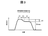
図3は図1の透過率分布フィルタ6の設置によって得た短軸方向の光強度分布の説明図である。図3に示した分布の領域X1の最大の照射エネルギ強度は可変アッテネータ3によって調節するが、その下限は基板1に成膜したアモルファスシリコン半導体薄膜が高エネルギ照射密度側の微結晶になる閾値以上に設定し、調節の上限は分布の後半の領域X3のエネルギ密度は少なくとも表層が溶融するエネルギ密度は、透過率分布フィルタによりΔEの値が0.1Emax以上である様に調節される。この場合、領域X1で生じた高エネルギ側の微結晶が領域X2のエネルギ密度照射で融合して大きな粒径になり、領域X3で表層のみ溶融させることによって突起を低減させる。
FIG. 3 is an explanatory diagram of the light intensity distribution in the minor axis direction obtained by installing the
図2の領域11と領域12の透過率の差が13%のフィルタで実験を行った結果、平均粒径が0.5μm以上となる照射エネルギ密度のマージンは、領域X1と領域X3の幅が等しい条件に固定した場合12%であり。突起の高さはアッテネータ透過率が上記マージンをカバーする80%から99%の範囲ではすべて70nm以下となった。
As a result of conducting an experiment using a filter having a transmittance difference of 13% between the
図4は透過率分布フィルタを用いないで複数回走査でレーザ光の照射エネルギ密度を変えた場合のシリコン半導体結晶の暗視野光学顕微鏡写真である。ここでは、アッテネータの透過率を変えて2回の走査を行って結晶化した。1回目の結晶化の走査のピッチ間隔が24μmであり、2回目の結晶化の走査ピッチは14μmである。図4(a)は、1回目のアッテネータ透過率が94%であり、2回目は1回目より透過率を6%低下させて照射したものである。この条件では、2回目の照射エネルギ密度も高エネルギ密度側の微結晶の閾値を超えて微結晶領域になっており、微結晶筋が14μmピッチで観察される。分布の裾の部分はエネルギ密度が低いので部分的に微結晶が融合し図4の写真では白っぽい領域となって観察される。 FIG. 4 is a dark-field optical micrograph of a silicon semiconductor crystal when the irradiation energy density of laser light is changed by scanning a plurality of times without using a transmittance distribution filter. Here, crystallization was performed by performing two scans while changing the transmittance of the attenuator. The pitch interval for the first crystallization scan is 24 μm, and the scan pitch for the second crystallization is 14 μm. In FIG. 4A, the first attenuator transmittance is 94%, and the second time irradiation is performed with the transmittance reduced by 6% from the first time. Under this condition, the irradiation energy density of the second time also exceeds the threshold value of the fine crystal on the high energy density side to become a fine crystal region, and fine crystal streaks are observed at a pitch of 14 μm. Since the energy density is low at the bottom of the distribution, the crystallites are partially fused, and a whitish region is observed in the photograph of FIG.
図4(b)は1回目のアッテネータ透過率が88%であり、2回目は1回目より透過率を6%低下させて照射したものである。写真の中で黒く見える領域が、1回目の照射で高エネルギ密度側の微結晶が発生して1回目のピッチに相当する24μmの周期となったものを、2回目の低エネルギ密度の照射によって微結晶が融合して粒径が大きくなった領域である。 In FIG. 4B, the first attenuator transmittance is 88%, and the second time is irradiated with the transmittance reduced by 6% from the first time. In the photograph, the region that appears black is a crystal having a high energy density side generated by the first irradiation and has a period of 24 μm corresponding to the first pitch. This is a region where the crystallites are fused to increase the particle size.
この様に、透過率分布フィルタを用いないで、多段の走査、かつ多段のエネルギ密度でレーザ光を照射する場合は、エネルギ密度によってシリコン半導体薄膜の試料には異なる走査ピッチ形状が現れることになる。これに対し、透過率分布フィルタを用いた場合は、試料上に現れる走査ピッチは1種類のみとなる。本実施例では、走査ピッチは走査速度できまり、レーザ2の繰り返し発振の1/300秒の時間間隔の移動量に等しい。
As described above, when laser light is irradiated with multi-stage scanning and multi-stage energy density without using a transmittance distribution filter, different scanning pitch shapes appear in the sample of the silicon semiconductor thin film depending on the energy density. . On the other hand, when the transmittance distribution filter is used, only one type of scanning pitch appears on the sample. In this embodiment, the scanning pitch is determined by the scanning speed, and is equal to the amount of movement in the time interval of 1/300 seconds of the repetitive oscillation of the
次に、実施例2を図5と図6を用いて説明する。図5は本発明の半導体製造方法を実現するレーザアニール装置の光学系の他例を説明する模式図である。図6は図5における透過率分布フィルタ6の表面の構成例を説明する模式的図である。この実施例は、図1で説明した実施例1におけるレーザ2とレーザアニール装置からなる構成は基本的に等しい。本実施例が実施例1の構成と異なる点は、透過率分布フィルタ16の設置場所が短軸ホモジナイザ5の直前であることと、透過率分布フィルタ16の透過率分布が図6に示すように短軸ホモジナイザ5内の各シリンドリカルレンズアレイ素子の内部の強度分布を制御する様にストライプ状になっていることである。なお、短軸ホモジナイザ5のシリンドリカルレンズアレイ5Aのレンズ素子数が5個の場合であって、さらにそのうち破線13で囲んだ様に3個分の広さのレーザビームが入射している場合を図示している。、図1の実施例と同様に、実際の数は9個で構成されており、破線13で囲んだ領域すなわちレーザ透過領域は、9個分以内の領域に設定されている。
Next, Example 2 will be described with reference to FIGS. FIG. 5 is a schematic view for explaining another example of the optical system of the laser annealing apparatus for realizing the semiconductor manufacturing method of the present invention. FIG. 6 is a schematic diagram for explaining a configuration example of the surface of the
図6において、破線13に囲んだ各領域(図6では3個の領域)が各レンズ素子の内部に光が透過する領域であり、この個々の領域内部の強度分布を透過率の異なる領域14と領域15で示される2種類のストライプ領域で制御する。試料基板の表面上の照射光強度分布は短軸ホモジナイザ5のレンズアレイ5Aの内部の強度分布の合成になるので、この透過率分布フィルタ16は、領域14と領域15の透過率の差で強度分布の段差分布を制御する。
In FIG. 6, each region (three regions in FIG. 6) surrounded by a
以下に位相シフトストライプマスクによる結晶化方法に透過率分布フィルタを適用した実施例を以下に説明する。図7は本発明の半導体製造方法を実現するレーザアニール装置の光学系のさらに他例を説明する模式図であり、位相シフトストライプ法によるレーザアニール装置の光学系を示す。本実施例は、前記した実施例1及び実施例2のラインビームによる通常のエキシマレーザアニール装置を利用したものである。透過率分布フィルタ6を設置する場所は、図1や図5と同じ位置とすることができる。図7では透過率分布フィルタの設置場所を図1と同じ場合とした。本実施例では、基板1の近傍に位相シフトストライプマスク41を設置した。このマスクの設置場所は1次結像面でも良い。
An embodiment in which a transmittance distribution filter is applied to a crystallization method using a phase shift stripe mask will be described below. FIG. 7 is a schematic diagram for explaining still another example of the optical system of the laser annealing apparatus for realizing the semiconductor manufacturing method of the present invention, and shows the optical system of the laser annealing apparatus by the phase shift stripe method. In this embodiment, the normal excimer laser annealing apparatus using the line beam of the first and second embodiments is used. The place where the
図8は位相シフトストライプマスクを用いてシリコン半導体薄膜の結晶化を行う方法の説明図である。位相シフトストライプマスク41は、図8に示すように、波長308nmに対して位相がほぼ180度シフトするパターンを3μmピッチで石英基板に凹凸ストライプパターンを形成したものであり、ラインビームに整形したレーザ光の長軸方向とはほぼ垂直方向になるようにストライプパターンを設けてある。そして、基板上に成膜した非晶質シリコン膜1Aの表面から0.9mmだけ離して設置する。他の構成は図1と同様である。位相シフトマスク透過後の強度分布は、パルスエキシマレーザはホモジナイザ光学系によって種々の位相の光が混在しているため、180度差の位相シフトマスク透過後の強度分布の谷の強度はゼロとはならない。このため、この最低強度を結晶化のしきい値以上にすれば1ショットで非晶質シリコンが残ることは無い。
FIG. 8 is an explanatory diagram of a method for crystallizing a silicon semiconductor thin film using a phase shift stripe mask. As shown in FIG. 8, the phase
図8は基板上に成膜した非晶質シリコン膜1Aの直上に設置した位相シフトストライプマスク41をパルスレーザ光が透過して基板上の非晶質シリコン薄膜1Aに照射した時の光強度分布と試料の結晶成長との関係を示している。位相シフトストライプマスク41のストライプパターンの周期は約3μmである。図示したように、本実施例では1ショットでレンズ光の照射領域全面が横方向に成長した結晶粒が形成される。結晶の成長方向はSLS法と同様にレーザ光強度の低い方から高い方へ向かって成長し、レーザ光強度のピーク位置に突起42が形成される。
FIG. 8 shows the light intensity distribution when the pulsed laser light is transmitted through the phase
図9は透過率分布フィルタと位相シフトストライプマスクのパターンと基板走査方向の説明図で、基板1上からレーザ光照射領域を見た図である。位相シフトストライプパターンと基板走査方向との成す角度は1度と設定し、走査速度は7.2mm/秒とした。この場合はパルス間の移動ピッチは約24μmとなる。また、パルス間の位相シフトストライプパターンと基板1との相対的なシフト量が、走査方向におけるストライプパターンの1周期以内で約0.5μmとなる。この量だけ1ショット毎に突起が形成する配列の位置がずれることになる。図25に突起の配列の位置が変化する周期と走査ピッチとの関係を示した。走査にともなって1ショットで結晶化する領域が、走査ピッチ毎にずれる。このとき突起の配列もずれる。したがって、突起の配列の位置が変化する周期は、走査ピッチに等しい。結晶が成長する方向はマスクパターンのピッチの方向であり、走査方向とほぼ直交する方向である。
FIG. 9 is an explanatory diagram of the transmittance distribution filter, the phase shift stripe mask pattern, and the substrate scanning direction, in which the laser beam irradiation region is viewed from above the
透過率分布フィルタは、図9に示すように、破線で示したラインビームに平行にかつ透過率のことなるM領域とN領域の境界がラインビーム内になる様に設置する。この透過率分布フィルタは石英製であり、M領域の表面には反射率1%のコーティング、N領域の表面には反射率11%以上のコーティング、裏面全体に反射率1%のコーティングを施したものである。これによって、M領域とN領域のエネルギ密度差は10%以上となっている。 As shown in FIG. 9, the transmittance distribution filter is installed in parallel to the line beam indicated by the broken line so that the boundary between the M region and the N region having different transmittances is within the line beam. This transmittance distribution filter is made of quartz. The surface of the M region is coated with a reflectance of 1%, the surface of the N region is coated with a reflectance of 11% or more, and the entire back surface is coated with a reflectance of 1%. Is. As a result, the energy density difference between the M region and the N region is 10% or more.
図10は透過率分布フィルタを位相シフトストライプマスクを用いた場合のシリコン半導体薄膜の結晶化の説明図である。上記した構成で、図10(a)の基板上に成膜した非晶質シリコン膜1Aに対してM領域の1ショット照射により、照射領域内は一括で横方向に成長した結晶粒が形成される。この時の平均結晶粒は突起間隔の約1/2となる(図10(b))。基板の走査に伴いM領域を通過中の複数ショットにより、多結晶膜厚方向に全体の溶融現象が繰り返されることによって、成長方向の平均粒径は突起間隔と等しくなる(図10(c))。但し、突起の形成位置は最後のショットで形成した突起35が最も高く、この位置が主に粒界となっている。それ以前のショットで形成された突起40は低いまま残っている場合が多い。N領域の照射は膜厚全体を溶融するエネルギより低いので粒界を形成することはできないが、低い突起のみを形成することが可能である。
FIG. 10 is an explanatory diagram of crystallization of a silicon semiconductor thin film when a phase distribution stripe mask is used for the transmittance distribution filter. With the above-described configuration, the
この低い突起形成において、M領域の最後のショットで形成された高い突起35は、N領域照射による突起形成のための表層のシリコンの流動によって低くなる(図10(d))。図10(d)はアッテネータ3の透過率を90%として結晶化を行った基板上のシリコン半導体薄膜を模式的に示す。結晶の粒界に存在する突起と結晶粒内に存在する突起とが存在する結晶となる。
しかも突起の配列の位置が変化する周期は1回の走査ピッチで決まるので約24μmの周期で1種類だけ形成されている多結晶膜が得られた。
In this low protrusion formation, the
In addition, since the period at which the position of the protrusion array changes is determined by one scanning pitch, a polycrystalline film formed with only one kind at a period of about 24 μm was obtained.
図11は透過率分布フィルタを位相シフトストライプマスク法に適用した場合と適用しない場合のシリコン半導体の結晶の走査型電子顕微鏡(SEM)で観察した写真である。図11(a)は透過率分布フィルタを用いて結晶化を行った結晶のSEM写真であり、図11(b)は透過率分布フィルタを用いないで結晶化を行った結晶のSEM写真である。図11の写真で白く観察されるところが表面に形成された突起に対応する部分である。図11(a)(b)における参照符号Lは平均粒径、また図11(b)におけるPoは主に結晶粒界の突起が配列している箇所、Piは主に結晶粒内の突起が配列している箇所を示す。 FIG. 11 is a photograph of a silicon semiconductor crystal observed with a scanning electron microscope (SEM) when the transmittance distribution filter is applied to the phase shift stripe mask method and when it is not applied. FIG. 11A is an SEM photograph of a crystal that has been crystallized using a transmittance distribution filter, and FIG. 11B is an SEM photograph of a crystal that has been crystallized without using a transmittance distribution filter. . A portion observed in white in the photograph of FIG. 11 is a portion corresponding to the protrusion formed on the surface. 11 (a) and 11 (b), the reference symbol L is the average grain size, Po in FIG. 11 (b) is a location where projections at the grain boundaries are mainly arranged, and Pi is mainly projections within the crystal grains. Indicates the location of the arrangement.
図11(b)に示された透過率分布フィルタを用いない場合は、結晶粒界の位置および結晶粒内に白く観察される高い突起が形成されているのが判るが、透過率分布フィルタを用いた図11(a)に示したものでは、突起が低いのでSEM写真で白く観察される高い突起が明瞭に観察されない。この場合の突起はPV値で70nm以下であった。 When the transmittance distribution filter shown in FIG. 11B is not used, it can be seen that high protrusions observed in white are formed in the crystal grain boundaries and the crystal grain boundaries. In the case shown in FIG. 11A used, since the protrusions are low, the high protrusions observed in white in the SEM photograph are not clearly observed. The protrusions in this case were 70 nm or less in terms of PV value.
図12は透過率分布フィルタを位相シフトストライプマスク法に適用した場合の突起の高さと透過率分布フィルタにおける透過率差の関係の説明図である。図12は図9における透過率分布フィルタのM領域とN領域の透過率の差に対して、突起の高さを10μm四方の領域で原子間力顕微鏡で評価した結果をグラフにしたものである。図12に示された結果から、透過率の差が10%以上で突起低減効果があり、15%以上あればPV値で70nm以下になることが判明した。 FIG. 12 is an explanatory diagram of the relationship between the height of the protrusion and the transmittance difference in the transmittance distribution filter when the transmittance distribution filter is applied to the phase shift stripe mask method. FIG. 12 is a graph showing the results of evaluating the height of the protrusions in an area of 10 μm square with an atomic force microscope with respect to the difference in transmittance between the M region and the N region of the transmittance distribution filter in FIG. . From the results shown in FIG. 12, it has been found that when the difference in transmittance is 10% or more, there is a protrusion reduction effect, and when it is 15% or more, the PV value is 70 nm or less.
結晶粒のサイズについては、位相シフトストライプパターンのピッチが3μmであるので、そのピッチの半分のサイズまで結晶が成長し、成長方向の結晶粒としては約1.5μmとなる。結晶の成長方向と垂直方向の粒界サイズは、0.5μm以下である。直交する2方向のアニール走査によって、平均粒径を2方向ともに1.5μmとすることができる。 Regarding the size of the crystal grains, since the pitch of the phase shift stripe pattern is 3 μm, the crystal grows to half the pitch, and the crystal grains in the growth direction are about 1.5 μm. The grain boundary size in the direction perpendicular to the crystal growth direction is 0.5 μm or less. By means of annealing scanning in two orthogonal directions, the average grain size can be 1.5 μm in both directions.
次に、SLS法に透過率分布制御フィルタを適用する実施例を説明する。図13は透過率分布制御フィルタをSLS法に適用したレーザアニール装置の光学系を説明する模式図である。また、図14はSLS法のレーザアニール装置に適用する透過率分布制御フィルタの一例の説明図である。図13に示したように、SLS法のレーザアニール装置(SLS結晶化装置)は光源2については実施例1と同じ構成としたものを利用する。すなわち、レーザ光源2の後段に、アッテネータ3、ホモジナイザ25、レンズ29、マスク26、イメージングレンズ27、そして非晶質シリコン半導体薄膜を成膜した基板1が置かれる移動ステージ30が順次に配列されている。そして、レンズ29とマスク26の間に本発明の透過率分布制御フィルタ31が挿入されている。アッテネータ3 とホモジナイザ25間及びイメージングレンズ27と移動ステージ30間には、入射した光を所定の角度で反射して光の方向を変化させるためのミラー23、24、28が各々配置されている。
Next, an embodiment in which a transmittance distribution control filter is applied to the SLS method will be described. FIG. 13 is a schematic diagram for explaining an optical system of a laser annealing apparatus in which a transmittance distribution control filter is applied to the SLS method. FIG. 14 is an explanatory diagram of an example of a transmittance distribution control filter applied to an SLS laser annealing apparatus. As shown in FIG. 13, a laser annealing apparatus (SLS crystallization apparatus) of the SLS method uses the
ホモジナイザ25はビーム整形とビーム内光強度を均一にするための光学系であり、レンズ29との組み合わせによってマスク26の位置に均一なビーム内強度分布を形成するようにしてある。図14におけるマスク26はアルミ製であり、マスク開口であるスリット26Aの幅が15μmであり、スリット26A間のマスクの幅も15μmとし、A領域とB領域はお互いに基板の走査方向に対してスリット26Aの間隔の配列周期の位相を15μmだけずらしてある。同様に、C領域とD領域もお互いに15μmだけずらし、且つA領域とC領域との周期位相のずれを互いに15μmとは異なる様に設定する。
The
レンズ27によってマスクパターンが1/5縮小して試料面上に投影される。
これによって基板上では、6ミクロン周期で3ミクロン幅の明暗の強度分布となる。マスク26のサイズは、50mm×50mmである。マスク26上でのA、B、C、Dの各領域の幅は各10ミリメートルである。
The mask pattern is reduced by 1/5 by the
As a result, a light and dark intensity distribution having a width of 3 microns and a period of 6 microns is obtained on the substrate. The size of the
図14に示した透過率分布フィルタ31はマスク26と同一サイズとし、石英基板の表面に反射率1%のコーティング膜を形成した領域32と反射率16%のコーティング膜を形成した領域33を形成し、裏面にはすべて反射率1%のコーティング膜を形成した。これによって領域32と領域33の透過率の差が15%であるフィルタをマスク近傍のすぐ上流側に設置した。マスクパターンの各領域が1ショットだけ照射されるように、パルス間隔が1/300秒の間の走査移動量が、パターンの各領域の試料面上での間隔に一致する様に設定される。
The
図15はSLS法に透過率分布フィルタを用いて得られるシリコン半導体薄膜の結晶化の説明図である。上記した条件で図15(a)の基板表面の非晶質シリコン薄膜1AにA領域照射(図15(b))→B領域照射(図15(c))→C領域照射(図15(d))→D領域照射(図15(e))のプロセスでレーザアニールされる。その結果、結晶化したシリコン半導体薄膜は、図15(e)に示したように、粒界位置に存在する突起39Aと、結晶粒内に存在する突起40とを有する結晶が得られた。しかも、突起の高さはすべて70nm以下となった。
FIG. 15 is an explanatory view of crystallization of a silicon semiconductor thin film obtained by using a transmittance distribution filter in the SLS method. Under the conditions described above, the amorphous silicon
この場合の結晶成長方向のサイズは3μmとなる。また、この場合の成長方向と直交方向の粒界のサイズも、実施例3の場合と同じように0.5μm以下となった。ほぼ直交する2方向のアニール走査によって、2方向の粒界サイズが3μmとすることも可能である。 In this case, the size in the crystal growth direction is 3 μm. In this case, the size of the grain boundary in the direction perpendicular to the growth direction was 0.5 μm or less as in the case of Example 3. It is also possible to set the grain boundary size in two directions to 3 μm by annealing scanning in two directions almost perpendicular to each other.
次に、本発明による多結晶シリコン半導体薄膜のラフネス評価方法の実施例を説明する。図16は粒径評価装置に表面ラフネス評価機能を追加した本発明の粒径評価方法を実現する粒径評価装置の光学系の模式図である。この装置の基本的な構成は特許文献11に開示されたものと同様である。図16において、参照符号69は枠であり、この枠69に、半導体薄膜を成膜した基板1の検査用(評価用)の波長532nmの連続発振レーザ光源60、基板1にレーザ光を照射するためのミラー62とレンズ65およびアパーチャ63からなる照射光学系、基板1からの散乱光角度分布を検出する光検出器アレイ67からなる基本構成が設置されている。これに本実施例のラフネス評価機能を追加するために、反射率と透過率を測定するための構成を追加する。
Next, an embodiment of a method for evaluating the roughness of a polycrystalline silicon semiconductor thin film according to the present invention will be described. FIG. 16 is a schematic diagram of an optical system of a particle size evaluation apparatus that realizes the particle size evaluation method of the present invention in which a surface roughness evaluation function is added to the particle size evaluation apparatus. The basic configuration of this apparatus is the same as that disclosed in
ラフネス評価機能を追加するための反射率と透過率を測定するための構成は、このレーザ光照射光学系にハーフミラー64と反射光強度をモニタするための光検出器66および透過光強度をモニタするための光検出器68とを6系統分追加する。さらに、検査用レーザ光の入射強度をモニタするための光検出器61を追加する。この追加によって、反射率と透過率を測定することが可能となる。
The configuration for measuring the reflectance and transmittance for adding the roughness evaluation function includes a
本実施例では、基板全面を短時間で計測するために6系統のマルチビームの構成を採用しているが、1 系統当りのレーザ光照射強度が約20mW以上あれば良いので、出力の高いレーザを検査用光源として用いれば系統数をさらに多くすることができるので、検査時間をさらに短縮化することが可能となる。 In this embodiment, a multi-beam configuration of 6 systems is adopted to measure the entire surface of the substrate in a short time. However, since the laser beam irradiation intensity per system should be about 20 mW or more, a high output laser As a light source for inspection, the number of systems can be further increased, so that the inspection time can be further shortened.
図17は図16に示した粒径評価装置を用いて測定した表面ラフネス量と原子間力顕微鏡で評価した表面ラフネスとの相関の説明図である。図17は前記実施例3の各種条件の多結晶膜の基板を測定した結果を原子間力顕微鏡で計測したPV値と比較したグラフである。縦軸は原子間力顕微鏡で計測したPV値であり、横軸は「1−(T+R)」である。但し、Tは透過率、Rは反射率を表している。図17における直線αと直線βは、それぞれ共通の傾きの相関直線であって、PV値の分布の上限と下限を示す。この様にPV値と「1−(T+R)」とには相関があることが分かる。 FIG. 17 is an explanatory diagram of the correlation between the amount of surface roughness measured using the particle size evaluation apparatus shown in FIG. 16 and the surface roughness evaluated with an atomic force microscope. FIG. 17 is a graph comparing the results of measuring the substrate of the polycrystalline film under various conditions of Example 3 with the PV value measured with an atomic force microscope. The vertical axis is the PV value measured with an atomic force microscope, and the horizontal axis is “1- (T + R)”. However, T represents the transmittance and R represents the reflectance. A straight line α and a straight line β in FIG. 17 are correlation straight lines having a common slope, and indicate the upper limit and the lower limit of the distribution of PV values. Thus, it can be seen that there is a correlation between the PV value and “1− (T + R)”.
図18は図16に示した粒径評価装置を用いて評価可能とした粒径に関する量と表面ラフネスに関する量との2次元分布による多結晶シリコン半導体薄膜の測定結果の一例の説明図である。図18は特許文献11に開示された内容による散乱角度分布幅に基づく粒径と1−(T+R)との2次元分布で表した多結晶膜の評価結果の例である。図17に示されたように、多結晶膜を粒径と表面ラフネスの2つについて管理基準を設定して、レーザアニール工程の管理を実施する。すなわち、平均粒径の管理基準を0.5μmとし、平均ラフネスとしてPV値70nm以下と設定し、どちらの管理基準もクリアしなければ再度結晶化し、両管理基準が満足するまで繰り返す。これによって、形成される多結晶膜はすべて両管理基準を満足する。
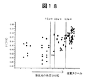
FIG. 18 is an explanatory view of an example of the measurement result of the polycrystalline silicon semiconductor thin film by the two-dimensional distribution of the amount related to the particle size and the amount related to the surface roughness that can be evaluated using the particle size evaluation apparatus shown in FIG. FIG. 18 is an example of an evaluation result of a polycrystalline film represented by a two-dimensional distribution of a particle size based on the scattering angle distribution width and 1- (T + R) based on the contents disclosed in
実施例5のラフネス評価方法は、実施例1、2、3、4で結晶化した多結晶シリコン半導体薄膜の表面ラフネスに対してすべて適用することができるが、実施例3と実施例4の横方向の成長した結晶については突起配列が規則正しいので、突起配列間隔と突起の高さの両方を評価可能な方法を説明する。 The roughness evaluation method of Example 5 can be applied to all of the surface roughness of the polycrystalline silicon semiconductor thin film crystallized in Examples 1, 2, 3, and 4. Since the protrusion arrangement is regular for the crystal grown in the direction, a method capable of evaluating both the protrusion arrangement interval and the protrusion height will be described.
この方法では、実施例5に示した構成の装置を用い、散乱光の角度分布を計測するアレイ検出器を2次元検出器とする。これによって、突起に由来する回折スポットの角度情報から突起間隔を評価し、スポットの強度より突起の高さを評価する。 In this method, an array detector that measures the angular distribution of scattered light is used as a two-dimensional detector using the apparatus having the configuration shown in the fifth embodiment. Thereby, the protrusion interval is evaluated from the angle information of the diffraction spot derived from the protrusion, and the height of the protrusion is evaluated from the intensity of the spot.
図19は本発明の実施例3における透過率分布フィルタを使用しないで3μmピッチの位相シフトストライプパターンを利用して形成した多結晶シリコン半導体薄膜の光回折パターを説明する写真である。図19(a)1方向にアニール走査して形成した多結晶シリコン半導体薄膜の光回折パターンであり、図19(b)は直交した2方向にアニール走査して形成した多結晶シリコン半導体薄膜の光回折パターンである。 FIG. 19 is a photograph illustrating an optical diffraction pattern of a polycrystalline silicon semiconductor thin film formed using a phase shift stripe pattern with a pitch of 3 μm without using the transmittance distribution filter in Example 3 of the present invention. FIG. 19A shows an optical diffraction pattern of a polycrystalline silicon semiconductor thin film formed by annealing scanning in one direction, and FIG. 19B shows light of the polycrystalline silicon semiconductor thin film formed by annealing scanning in two orthogonal directions. It is a diffraction pattern.
図19(a)(b)から、それぞれ突起に由来する回折スポットが観察され、その配列はアニール走査方向に依存している事が分かる。回折スポットの強度は、突起の高さと検査用レーザ光の径に含まれる突起の数と突起の配列秩序に依存する。検査用のレーザ光の径は一定であるので突起の数は一定であり、ピッチが一定の位相シフトマスクを用いている場合は配列秩序は一定であるので、回折スポットの光強度は突起の高さのみに依存する量となる。 19 (a) and 19 (b), diffraction spots derived from protrusions are observed, and it can be seen that the arrangement depends on the annealing scanning direction. The intensity of the diffraction spot depends on the height of the protrusion, the number of protrusions included in the diameter of the inspection laser beam, and the arrangement order of the protrusions. Since the diameter of the laser beam for inspection is constant, the number of protrusions is constant, and when a phase shift mask with a constant pitch is used, the arrangement order is constant, so the light intensity of the diffraction spot is high. The amount depends only on the size.
図24は、本発明の実施例3における透過率分布フィルタを使用しないで2μmピッチの位相シフトストライプパターンを利用して、照射エネルギ密度を変えて一方向のアニール走査で形成した多結晶シリコン半導体薄膜の光回折パターンとシート抵抗との関係である。横軸の透過率は照射レーザ強度に比例する。シート抵抗は粒径が大きいほど小さく、ほぼ逆数の関係が成り立つ。図11に示したように結晶粒が細長く、結晶の長軸方向のシート抵抗値は短軸方向のシート抵抗値と比べると、透過率84%で約半分程度である事が分かる。このときの光回折パターン(B)における結晶の長軸方向の角度分布と短軸方向の角度分布を比較すると、長軸方向の角度分布の幅が約半分になっている事が分かる。これに対して透過率が72%でレーザ強度が弱すぎる場合は、結晶粒の長軸方向と短軸方向のシート抵抗値との比率は1に近いが、これに対応して散乱光の長軸方向の角度分布の幅と短軸方向の角度分布の幅もほぼ等しくなっている事が分かる。以上によって、結晶粒が細長い場合も散乱光の角度分布幅で粒径が評価できることが分かる。 FIG. 24 shows a polycrystalline silicon semiconductor thin film formed by annealing scanning in one direction while changing the irradiation energy density using a phase shift stripe pattern with a pitch of 2 μm without using the transmittance distribution filter in Example 3 of the present invention. The relationship between the light diffraction pattern and the sheet resistance. The transmittance on the horizontal axis is proportional to the irradiation laser intensity. The sheet resistance is smaller as the particle size is larger, and a substantially inverse relationship is established. As shown in FIG. 11, it can be seen that the crystal grains are elongated, and the sheet resistance value in the major axis direction of the crystal is about half of the transmittance of 84% compared to the sheet resistance value in the minor axis direction. When the angle distribution in the major axis direction and the angle distribution in the minor axis direction of the crystal in the light diffraction pattern (B) at this time are compared, it can be seen that the width of the angle distribution in the major axis direction is about half. On the other hand, when the transmittance is 72% and the laser intensity is too weak, the ratio of the sheet resistance value in the major axis direction to the minor axis direction of the crystal grains is close to 1, but the length of the scattered light is corresponding to this. It can be seen that the width of the angular distribution in the axial direction is substantially equal to the width of the angular distribution in the minor axis direction. From the above, it can be seen that the grain size can be evaluated by the angular distribution width of the scattered light even when the crystal grains are elongated.
図20は本発明の実施例3と実施例4で形成された多結晶シリコン半導体薄膜の回折パターン上の回折スポットの位置と突起の間隔との関係の説明図である。図20におけるλはレーザ光の波長、dは基板上に成膜した多結晶シリコン半導体薄膜に形成された突起(ここではtで示す)の間隔、Lは試料と回折パターン面との距離、pは「p=L×tan(arcsin(mλ)/d)」である。図20に示した様に、突起tの間隔dは、回折面上における回折スポットの位置pによって評価することができる。すなわち、回折スポットが形成する方向は各突起から発生する散乱光の行路差が波長の整数倍に比例するとして得られる関数により、突起間隔を回折スポットの位置から評価することができる。この突起の評価方法は、SLS法によって形成した多結晶シリコン薄膜の突起の評価にも適用することができる。 FIG. 20 is an explanatory diagram of the relationship between the position of the diffraction spot on the diffraction pattern of the polycrystalline silicon semiconductor thin film formed in Example 3 and Example 4 of the present invention and the interval between the protrusions. In FIG. 20, λ is the wavelength of the laser beam, d is the distance between the protrusions (shown here as t) formed on the polycrystalline silicon semiconductor thin film formed on the substrate, L is the distance between the sample and the diffraction pattern surface, p Is “p = L × tan (arcsin (mλ) / d)”. As shown in FIG. 20, the distance d between the protrusions t can be evaluated by the position p of the diffraction spot on the diffraction surface. That is, the direction in which the diffraction spot is formed can be evaluated from the position of the diffraction spot by a function obtained by assuming that the path difference of the scattered light generated from each protrusion is proportional to an integral multiple of the wavelength. This projection evaluation method can also be applied to the evaluation of projections of a polycrystalline silicon thin film formed by the SLS method.
以上により、位相シフトストライプ法やSLS法の様に突起が規則正しく配列する結晶化する製造工程において、透過率分布フィルタを利用した突起低減方法を採用し、さらに光回折スポットの強度を測定してその測定値に管理基準を設定する。管理基準の強度を越える領域があれば、その領域を照射エネルギ密度を変えて再度結晶化することを、管理基準が満足するまで繰る返すことにより、突起の高さをPV値ですべて70nm以下にする事ができる。 As described above, in the manufacturing process for crystallizing the protrusions regularly arranged as in the phase shift stripe method or the SLS method, the protrusion reduction method using the transmittance distribution filter is adopted, and the intensity of the light diffraction spot is further measured. Set control criteria for measured values. If there is a region that exceeds the intensity of the management standard, the height of the projections is reduced to 70 nm or less in terms of PV value by repeating the crystallization with changing the irradiation energy density until the management standard is satisfied. I can do it.
次に、上記に記述した各方法で作成する多結晶薄膜を利用して形成した薄膜トランジスタとこの薄膜トランジスタを含む駆動回路や画素回路で構成した表示装置の実施例を説明する。 Next, an embodiment of a display device constituted by a thin film transistor formed by using a polycrystalline thin film produced by each method described above and a drive circuit or a pixel circuit including the thin film transistor will be described.
図21は本発明の製造方法で形成した多結晶シリコン薄膜を用いた薄膜トランジスタを含む表示装置としてのアクティブ・マトリクス型の液晶表示装置の要部構成例を説明する断面図である。この液晶表示装置は次のように構成されている。即ち、薄膜トランジスタ515、カラーフィルタ510及び画素電極511を備えるガラス基板501と、対向電極513を有する対向ガラス基板514との対向間隙に液晶512を介在させて封止している。なお、液晶512と各基板の境界には配向制御膜が成膜されるが、図示を省略した。
FIG. 21 is a cross-sectional view for explaining a configuration example of a main part of an active matrix type liquid crystal display device as a display device including a thin film transistor using a polycrystalline silicon thin film formed by the manufacturing method of the present invention. This liquid crystal display device is configured as follows. That is, the
ガラス基板501の表面には、アンダーコート層(酸化シリコン膜および窒化シリコン膜)502が形成され、その上に非晶質シリコン半導体層が形成されて、前記製造方法の実施例で説明したように、本発明に係るレーザアニールにより多結晶シリコン薄膜の層に改質されている。このレーザアニールにより得た多結晶シリコン薄膜の層に薄膜トランジスタ515が作り込まされている。即ち、多結晶シリコン半導体薄膜からなる半導体層503の両側に不純物をドープすることにより、多結晶シリコンのソース半導体層504aおよび多結晶シリコンのドレイン層504bが形成され、その上にゲート酸化膜(ゲート絶縁層)505を介してゲート電極506が形成されている。
An undercoat layer (silicon oxide film and silicon nitride film) 502 is formed on the surface of the
ソース/ドレイン電極508が、層間絶縁膜507に形成された接続孔(コンタクトホール)を介して、それぞれソース半導体層504aおよびドレイン半導体層504bに接続され、その上に保護膜509が設けられる。そして、保護膜509上にカラーフィルタ510及び画素電極511が形成されている。特に、本発明の実施例3および実施例4のレーザアニール法では、1 回の走査による結晶は、結晶粒のサイズが方向によって異なるので、薄膜トランジスタ515のソース/ドレイン電極508の方向(すなわち、チャネル方向)を多結晶シリコン半導体結晶粒のサイズの大きい方向になるように揃える。なお、走査方向を2方向としてアニールした多結晶シリコン半導体結晶では、この様に揃える必要は無い。
The source /
この薄膜トランジスタは液晶表示装置の画素回路を構成し、図示しない走査線駆動回路からの選択信号で選択され、図示しない信号線駆動回路から供給される画像信号で画素電極511が駆動される。駆動された画素電極511と、対向ガラス基板514の内面に有する対向電極513の間に電界が形成される。この電界により、液晶512の分子配向方向が制御されて表示がなされる。
This thin film transistor constitutes a pixel circuit of a liquid crystal display device, is selected by a selection signal from a scanning line driving circuit (not shown), and the
なお、上記した走査線駆動回路や信号線駆動回路を構成する薄膜トランジスタも上記画素回路と同様の多結晶シリコン半導体薄膜で形成することもできる。また、本発明は液晶表示装置に限らず、アクティブ・マトリクス型の他の表示装置、例えば有機EL表示装置やプラズマ表示装置、その他の各種表示装置にも適用でき、あるいは太陽電池を構成する半導体薄膜の製造にも同様に適用することができる。 Note that the thin film transistors constituting the above-described scanning line driving circuit and signal line driving circuit can also be formed of a polycrystalline silicon semiconductor thin film similar to the pixel circuit. The present invention is not limited to a liquid crystal display device, but can be applied to other active matrix type display devices such as an organic EL display device, a plasma display device, and other various display devices, or a semiconductor thin film constituting a solar cell. It can be applied to the manufacture of
以上のように、本発明のレーザアニール法を用いた半導体製造方法とその評価方法を採用することにより、優れた特性を示す本発明の薄膜トランジスタを量産することができ、この薄膜トランジスタを用いることで、高品質な本発明の表示装置を非常に高い歩留まりで製造することができる。 As described above, by adopting the semiconductor manufacturing method using the laser annealing method of the present invention and its evaluation method, the thin film transistor of the present invention exhibiting excellent characteristics can be mass-produced. By using this thin film transistor, A high-quality display device of the present invention can be manufactured with a very high yield.
ガラス等の絶縁基板上に薄膜トランジスタに代表されるアクティブ素子を形成して、画像表示装置を形成する場合、あるいは太陽電池を形成する場合の当該半導体薄膜の表面ラフネスを低減した半導体基板として利用することができる。 When an active element typified by a thin film transistor is formed on an insulating substrate such as glass to form an image display device or a solar cell, the semiconductor thin film should be used as a semiconductor substrate with reduced surface roughness. Can do.
1 シリコン半導体薄膜を成膜した基板(試料基板)
1A 基板上に成膜されたシリコン半導体膜
2 結晶化用レーザ光源
3 アッテネータ
4 長軸ホモジナイザ
5 短軸ホモジナイザ
5A 短軸ホモジナイザの前段のシリンドリカルレンズアレイ
5B 短軸ホモジナイザの後段のシリンドリカルレンズアレイ
6 透過率分布フィルタ
7 ミラー
8 シリンドリカルレンズ
9 レーザ光
10 シリンドリカルレンズ
11 12の領域より透過率が相対的に低い領域
12 11の領域より透過率が相対的に高い領域
13 短軸ホモジナイザのシリンドリカルレンズアレイ各素子に対応する光透過領域
14 15の領域より透過率が相対的に低い領域
15 14の領域より透過率が相対的に高い領域
16 透過率分布フィルタ
23 ミラー
24 ミラー
25 ホモジナイザ
26 マスク
27 イメージングレンズ
28 ミラー
29 レンズ
30 移動ステージ
31 透過率分布フィルタ
32 33の領域より透過率が相対的に高い領域
33 32の領域より透過率が相対的に低い領域
41 位相シフトストライプマスク
50 透過率分布フィルタ
60 検査用レーザ光源
61 入射光強度モニタ用光検出器(1系統)
62 ハーフミラー(6系統)
63 基板からの反射光の強度モニタ用光検出器(6系統)
64 基板からの透過光の強度モニタ用光検出器(6系統)
65 アパーチャ
66 基板からの散乱光強度の角度分布用アレイ検出器(6系統)
501 ガラス基板
502 アンダーコート層
503 多結晶シリコン膜
504a 多結晶シリコンのソース層
504b 多結晶シリコンドレイン層
505 ゲート酸化膜
507 層間絶縁膜
506 ゲート電極
508 ソース/ドレイン電極
509 保護膜
510 カラーフィルタ510
511 画素電極
512 液晶
513 対向電極
514 対向ガラス基板。
1 Substrate on which a silicon semiconductor thin film is formed (sample substrate)
1A Silicon semiconductor film formed on a
Cylindrical lens array in front of 5A short axis homogenizer
5B Cylindrical lens array downstream of
62 Half mirror (6 lines)
63 Light detector for monitoring intensity of reflected light from substrate (6 systems)
64 Light detector for monitoring the intensity of light transmitted from the substrate (6 systems)
65
501
Claims (20)
前記ラインビーム内の光強度分布を一定の透過率面内分布に制御する透過率分布フィルタを透過させることによって前記結晶化を行うことを特徴とする半導体薄膜の改質方法。 The amorphous semiconductor thin film is modified into a polycrystalline semiconductor thin film by irradiating and crystallizing the amorphous semiconductor thin film while scanning the line beam shaped laser beam in a direction crossing the long axis direction of the line beam. A method for modifying a semiconductor thin film,
A method for modifying a semiconductor thin film, characterized in that the crystallization is performed by transmitting a light intensity distribution in the line beam through a transmittance distribution filter that controls the light transmittance distribution to a constant transmittance in-plane distribution.
前記レーザ光の前記走査方向における照射レーザ光内の光強度分布を、改質された前記多結晶半導体薄膜が厚さ方向で全体が溶融するエネルギを有する領域と該多結晶半導体薄膜が厚さ方向で表層のみが溶融するエネルギを有する領域とからなる強度分布に制御して、結晶化を行うことを特徴とする半導体薄膜の改質方法。 A method for modifying a semiconductor thin film, wherein the amorphous semiconductor thin film is modified into a polycrystalline semiconductor thin film by irradiating and crystallizing the amorphous semiconductor thin film while scanning with a laser beam,
The intensity distribution of the laser beam in the scanning direction of the laser beam in the scanning laser beam is changed to a region in which the modified polycrystalline semiconductor thin film has energy to melt in the thickness direction and the polycrystalline semiconductor thin film in the thickness direction. A method for reforming a semiconductor thin film characterized in that crystallization is carried out by controlling the intensity distribution to include a region having energy where only the surface layer melts.
照射レーザビーム内の光強度分布を、一定の透過率面内分布を有する透過率分布フィルタとスリットマスクとを透過させることで前記照射レーザ光内の光強度分布を制御することを特徴とする請求項4に記載の半導体薄膜の改質方法。 A method for modifying a semiconductor thin film, wherein the amorphous semiconductor thin film is modified into a polycrystalline semiconductor thin film by irradiating and crystallizing the amorphous semiconductor thin film while scanning with a laser beam,
The light intensity distribution in the irradiation laser beam is controlled by transmitting the light intensity distribution in the irradiation laser beam through a transmittance distribution filter having a constant transmittance in-plane distribution and a slit mask. Item 5. A method for modifying a semiconductor thin film according to Item 4.
前記ラインビーム内の光強度分布を一定の透過率面内分布に制御する透過率分布フィルタを装置内光学系の結像面近傍に設置することによって、照射ビーム強度分布プロファイルを制御して前記結晶化を行うことを特徴とするレーザアニール装置。 A laser annealing apparatus for modifying an amorphous semiconductor thin film into a polycrystalline semiconductor thin film by irradiating and crystallizing the amorphous semiconductor thin film while scanning with a laser beam,
By installing a transmittance distribution filter for controlling the light intensity distribution in the line beam to a constant transmittance in-plane distribution in the vicinity of the imaging plane of the optical system in the apparatus, the irradiation beam intensity distribution profile is controlled to control the crystal A laser annealing apparatus characterized by performing the process.
前記改質された多結晶半導体薄膜の結晶粒は一方向に横方向成長した形状を有し、且つ前記結晶粒の粒界と粒内とに突起が存在し、且つ前記突起の前記一方向の配列の位置が変化する周期が1種類のみ存在することを特徴とする多結晶半導体膜。 A polycrystalline semiconductor thin film modified by irradiating and crystallizing an amorphous semiconductor thin film while scanning a line beam shaped laser beam in a direction crossing the longitudinal direction of the line beam,
The crystal grains of the modified polycrystalline semiconductor thin film have a shape that is laterally grown in one direction, and there are protrusions at grain boundaries and in the grains, and the protrusions are in the one direction. A polycrystalline semiconductor film characterized in that there is only one type of period in which the position of the array changes.
前記改質された多結晶半導体薄膜の結晶粒は面内二方向に横方向成長した形状を有し、且つ前記結晶粒の粒界と粒内とに突起が存在し、且つ前記突起の前記方向の配列の位置が変化する周期が各方向で1種類のみ存在することを特徴とする多結晶半導体薄膜。 A polycrystalline semiconductor thin film modified by irradiating and crystallizing an amorphous semiconductor thin film while scanning a line beam shaped laser beam in a direction crossing the longitudinal direction of the line beam,
The crystal grains of the modified polycrystalline semiconductor thin film have a shape grown laterally in two in-plane directions, and there are protrusions at grain boundaries and in the grains, and the direction of the protrusions A polycrystalline semiconductor thin film characterized in that there is only one type of period in which the position of the arrangement of each changes in each direction.
前記半導体膜にレーザ光を照射し反射率と透過率とを測定し、「1−(反射率+透過率)」の値を計測することを特徴とする半導体薄膜評価装置。 A semiconductor film evaluation apparatus for evaluating a semiconductor film on a transparent substrate,
A semiconductor thin film evaluation apparatus, wherein the semiconductor film is irradiated with laser light to measure a reflectance and a transmittance, and a value of “1- (reflectance + transmittance)” is measured.
前記多結晶半導体薄膜の光回折パターン面上の回折スポットの強度および散乱光強度の角度分布を計測する事によって多結晶の表面ラフネスと粒径の評価を行うことを特徴とする多結晶半導体薄膜評価装置。 A polycrystalline semiconductor thin film evaluation apparatus for evaluating a polycrystalline semiconductor film,
Polycrystalline semiconductor thin film evaluation characterized in that the polycrystalline semiconductor thin film is evaluated for surface roughness and grain size by measuring the angular distribution of diffraction spot intensity and scattered light intensity on the surface of the optical diffraction pattern of the polycrystalline semiconductor thin film apparatus.
The grain boundaries include crystal grains having a unidirectional size of 1.5 μm or more and a grain boundary in the other direction substantially orthogonal to the one direction of 1.5 μm or more, and are arranged on a straight line substantially orthogonal to the surface. An image display device comprising a polycrystalline semiconductor film having a protrusion and a height of the protrusion represented by a PV value of 70 nm or less within an area of several μm square.
Priority Applications (6)
| Application Number | Priority Date | Filing Date | Title |
|---|---|---|---|
| JP2003364539A JP2005129769A (en) | 2003-10-24 | 2003-10-24 | Method for modifying semiconductor thin film, modified semiconductor thin film, method for evaluating the same, thin film transistor formed of semiconductor thin film, and image display device having circuit constituted by using the thin film transistor |
| TW093119079A TW200515485A (en) | 2003-10-24 | 2004-06-29 | Method for modifying semiconductor thin film, modified semiconductor thin film, method for evaluating the same, thin film transistor formed of semiconductor thin film, and image display device having circuit constituted by using the thin film transistor |
| KR1020040055369A KR101151312B1 (en) | 2003-10-24 | 2004-07-16 | A reform method of semiconductor thin film, a reformed semiconductor thin film and a test method thereof, a thin film transistor made of the semiconductor film and image displayer having a circuit using the semiconductor thin film |
| US10/900,365 US7151046B2 (en) | 2003-10-24 | 2004-07-28 | Semiconductor thin film decomposing method, decomposed semiconductor thin film, decomposed semiconductor thin film evaluation method, thin film transistor made of decomposed semiconductor thin film, and image display device having circuit constituted of thin film transistors |
| CNB2004100590471A CN100437906C (en) | 2003-10-24 | 2004-07-29 | Semiconductor thin film and modifying method, estimating method and application thereof |
| US11/449,664 US20060254497A1 (en) | 2003-10-24 | 2006-06-09 | Semiconductor thin film decomposing method, decomposed semiconductor thin film, decomposed semiconductor thin film evaluation method, thin film transistor made of decomposed semiconductor thin film, and image display device having circuit constituted of thin film transistors |
Applications Claiming Priority (1)
| Application Number | Priority Date | Filing Date | Title |
|---|---|---|---|
| JP2003364539A JP2005129769A (en) | 2003-10-24 | 2003-10-24 | Method for modifying semiconductor thin film, modified semiconductor thin film, method for evaluating the same, thin film transistor formed of semiconductor thin film, and image display device having circuit constituted by using the thin film transistor |
Related Child Applications (1)
| Application Number | Title | Priority Date | Filing Date |
|---|---|---|---|
| JP2010002729A Division JP2010153876A (en) | 2010-01-08 | 2010-01-08 | Method for reforming semiconductor thin film, reformed semiconductor thin film, method for evaluating reformed semiconductor thin film, thin film transistor formed of the semiconductor thin film, and image display device with circuit constituted using the thin film transistor |
Publications (1)
| Publication Number | Publication Date |
|---|---|
| JP2005129769A true JP2005129769A (en) | 2005-05-19 |
Family
ID=34643489
Family Applications (1)
| Application Number | Title | Priority Date | Filing Date |
|---|---|---|---|
| JP2003364539A Pending JP2005129769A (en) | 2003-10-24 | 2003-10-24 | Method for modifying semiconductor thin film, modified semiconductor thin film, method for evaluating the same, thin film transistor formed of semiconductor thin film, and image display device having circuit constituted by using the thin film transistor |
Country Status (5)
| Country | Link |
|---|---|
| US (2) | US7151046B2 (en) |
| JP (1) | JP2005129769A (en) |
| KR (1) | KR101151312B1 (en) |
| CN (1) | CN100437906C (en) |
| TW (1) | TW200515485A (en) |
Cited By (8)
| Publication number | Priority date | Publication date | Assignee | Title |
|---|---|---|---|---|
| WO2010001518A1 (en) * | 2008-07-02 | 2010-01-07 | 信越半導体株式会社 | Silicon single crystal wafer, process for producing silicon single crystal wafer, and method for evaluating silicon single crystal wafer |
| JP2010283073A (en) * | 2009-06-03 | 2010-12-16 | V Technology Co Ltd | Laser annealing method, and laser annealing apparatus |
| JP2010541250A (en) * | 2007-09-25 | 2010-12-24 | ザ トラスティーズ オブ コロンビア ユニヴァーシティ イン ザ シティ オブ ニューヨーク | Method for producing high uniformity in thin film transistor devices fabricated on laterally crystallized thin films |
| JP2011192785A (en) * | 2010-03-15 | 2011-09-29 | Hitachi High-Technologies Corp | Polycrystalline silicon thin film inspection method and device thereof |
| JP2011204911A (en) * | 2010-03-25 | 2011-10-13 | Japan Steel Works Ltd:The | Method for manufacturing anneal processed body and laser annealing apparatus |
| WO2018101154A1 (en) * | 2016-11-30 | 2018-06-07 | 株式会社ブイ・テクノロジー | Laser irradiation device and method for manufacturing thin film transistor |
| JP2020047684A (en) * | 2018-09-18 | 2020-03-26 | 株式会社オプトピア | Light source device and line beam homogenizer using the same |
| WO2020137399A1 (en) * | 2018-12-27 | 2020-07-02 | 株式会社ブイ・テクノロジー | Laser annealing method and laser annealing device |
Families Citing this family (47)
| Publication number | Priority date | Publication date | Assignee | Title |
|---|---|---|---|---|
| US6555449B1 (en) | 1996-05-28 | 2003-04-29 | Trustees Of Columbia University In The City Of New York | Methods for producing uniform large-grained and grain boundary location manipulated polycrystalline thin film semiconductors using sequential lateral solidfication |
| AU2003258289A1 (en) | 2002-08-19 | 2004-03-03 | The Trustees Of Columbia University In The City Of New York | A single-shot semiconductor processing system and method having various irradiation patterns |
| JP4873858B2 (en) | 2002-08-19 | 2012-02-08 | ザ トラスティーズ オブ コロンビア ユニヴァーシティ イン ザ シティ オブ ニューヨーク | Method and apparatus for laser crystallization processing of film region of substrate and structure of such film region to minimize edge region |
| US7164152B2 (en) | 2003-09-16 | 2007-01-16 | The Trustees Of Columbia University In The City Of New York | Laser-irradiated thin films having variable thickness |
| WO2005029546A2 (en) | 2003-09-16 | 2005-03-31 | The Trustees Of Columbia University In The City Of New York | Method and system for providing a continuous motion sequential lateral solidification for reducing or eliminating artifacts, and a mask for facilitating such artifact reduction/elimination |
| WO2005029549A2 (en) | 2003-09-16 | 2005-03-31 | The Trustees Of Columbia University In The City Of New York | Method and system for facilitating bi-directional growth |
| TWI359441B (en) | 2003-09-16 | 2012-03-01 | Univ Columbia | Processes and systems for laser crystallization pr |
| WO2005034193A2 (en) | 2003-09-19 | 2005-04-14 | The Trustees Of Columbia University In The City Ofnew York | Single scan irradiation for crystallization of thin films |
| US7645337B2 (en) | 2004-11-18 | 2010-01-12 | The Trustees Of Columbia University In The City Of New York | Systems and methods for creating crystallographic-orientation controlled poly-silicon films |
| US8221544B2 (en) | 2005-04-06 | 2012-07-17 | The Trustees Of Columbia University In The City Of New York | Line scan sequential lateral solidification of thin films |
| CN100362420C (en) * | 2005-07-27 | 2008-01-16 | 大连理工大学 | Method for improving optical characteristics of rare earth mixed aluminum oxide thin film utilizing laser annealing |
| KR101287314B1 (en) | 2005-12-05 | 2013-07-17 | 더 트러스티이스 오브 콜롬비아 유니버시티 인 더 시티 오브 뉴욕 | Systems and methods for processing a film, and thin films |
| KR20070078132A (en) * | 2006-01-26 | 2007-07-31 | 삼성전자주식회사 | Silicon crystallizing mask, silicon crystallizing apparatus having the mask and silicon crystallizing method using the apparatus |
| JP2007208174A (en) * | 2006-02-06 | 2007-08-16 | Fujifilm Corp | Laser annealing technique, semiconductor film, semiconductor device, and electro-optical device |
| JP2008244374A (en) * | 2007-03-29 | 2008-10-09 | Nec Lcd Technologies Ltd | Manufacturing method for semiconductor thin film, semiconductor thin film and thin film transistor |
| CN101680107B (en) | 2007-04-24 | 2013-04-10 | Limo专利管理有限及两合公司 | Method for restructuring semiconductor layers |
| US20090046757A1 (en) * | 2007-08-16 | 2009-02-19 | Semiconductor Energy Laboratory Co., Ltd. | Laser irradiation apparatus, laser irradiation method, and manufacturing method of semiconductor device |
| TW200942935A (en) | 2007-09-21 | 2009-10-16 | Univ Columbia | Collections of laterally crystallized semiconductor islands for use in thin film transistors and systems and methods for making same |
| JP5443377B2 (en) | 2007-11-21 | 2014-03-19 | ザ トラスティーズ オブ コロンビア ユニヴァーシティ イン ザ シティ オブ ニューヨーク | Preparation system and method for preparing epitaxially oriented thick films |
| WO2009067688A1 (en) | 2007-11-21 | 2009-05-28 | The Trustees Of Columbia University In The City Of New York | Systems and methods for preparing epitaxially textured polycrystalline films |
| US7906392B2 (en) | 2008-01-15 | 2011-03-15 | Sandisk 3D Llc | Pillar devices and methods of making thereof |
| JP5438986B2 (en) * | 2008-02-19 | 2014-03-12 | 株式会社半導体エネルギー研究所 | Method for manufacturing photoelectric conversion device |
| KR100864062B1 (en) * | 2008-02-22 | 2008-10-16 | 한국철강 주식회사 | A device to pattern solar cell module |
| US8569155B2 (en) | 2008-02-29 | 2013-10-29 | The Trustees Of Columbia University In The City Of New York | Flash lamp annealing crystallization for large area thin films |
| WO2010056990A1 (en) | 2008-11-14 | 2010-05-20 | The Trustees Of Columbia University In The City Of New York | Systems and methods for the crystallization of thin films |
| US9087696B2 (en) | 2009-11-03 | 2015-07-21 | The Trustees Of Columbia University In The City Of New York | Systems and methods for non-periodic pulse partial melt film processing |
| US9646831B2 (en) | 2009-11-03 | 2017-05-09 | The Trustees Of Columbia University In The City Of New York | Advanced excimer laser annealing for thin films |
| US8440581B2 (en) | 2009-11-24 | 2013-05-14 | The Trustees Of Columbia University In The City Of New York | Systems and methods for non-periodic pulse sequential lateral solidification |
| JP2013527120A (en) * | 2010-06-03 | 2013-06-27 | ザ トラスティーズ オブ コロンビア ユニヴァーシティ イン ザ シティ オブ ニューヨーク | Single scan line scan crystallization using superimposed scan elements |
| TWI517965B (en) * | 2010-07-12 | 2016-01-21 | Dexerials Corp | Manufacturing method of mother board, manufacturing method of alignment film, manufacturing method of phase difference plate, and manufacturing method of display device |
| KR101666661B1 (en) * | 2010-08-26 | 2016-10-17 | 삼성디스플레이 주식회사 | Thin film transistor substrate and flat panel display apparatus |
| EP2869963B1 (en) * | 2012-07-04 | 2016-09-28 | Saint-Gobain Glass France | Device for and method of laser processing of large-scale substrates using at least two portals |
| US8937770B2 (en) | 2012-07-24 | 2015-01-20 | Coherent Gmbh | Excimer laser apparatus projecting a beam with a selectively variable short-axis beam profile |
| CN103835000A (en) * | 2012-11-20 | 2014-06-04 | 上海华虹宏力半导体制造有限公司 | Method for high temperature improvement of polysilicon surface roughness |
| CN103839790B (en) * | 2012-11-23 | 2016-09-28 | 中芯国际集成电路制造(上海)有限公司 | Laser anneal device and method for annealing |
| US9529239B2 (en) | 2013-12-31 | 2016-12-27 | Shenzhen China Star Optoelectronics Technologies Co., Ltd. | Manufacturing method and repairing method for display device as well as liquid crystal display panel |
| CN103995378B (en) * | 2013-12-31 | 2016-10-05 | 深圳市华星光电技术有限公司 | Manufacture the method for display device and restorative procedure and display panels |
| EP2899749A1 (en) * | 2014-01-24 | 2015-07-29 | Excico France | Method for forming polycrystalline silicon by laser irradiation |
| CN103934577B (en) * | 2014-03-12 | 2017-02-15 | 苏州福唐智能科技有限公司 | Stray-light-free laser processing system with adjustable cutting width |
| WO2015171335A1 (en) | 2014-05-06 | 2015-11-12 | Applied Materials, Inc. | Directional treatment for multi-dimensional device processing |
| TWI577488B (en) * | 2014-11-17 | 2017-04-11 | 財團法人工業技術研究院 | Surface processing method |
| KR102531651B1 (en) * | 2016-01-06 | 2023-05-11 | 삼성디스플레이 주식회사 | Laser crystalling apparatus |
| CN105654499B (en) * | 2016-01-27 | 2018-02-16 | 中国科学院力学研究所 | A kind of image evaluation method of laser surface modification |
| CN105957023B (en) * | 2016-04-19 | 2018-11-23 | 南京工程学院 | A kind of enhancing of laser rays stripe pattern and denoising method based on chroma space |
| TWI637805B (en) * | 2016-10-25 | 2018-10-11 | 財團法人工業技術研究院 | Laser processing system and method for metallic surface |
| KR20220022016A (en) * | 2020-08-14 | 2022-02-23 | 삼성디스플레이 주식회사 | Apparatus and method for manufacturing a display device |
| DE102020126269A1 (en) * | 2020-10-07 | 2022-04-07 | Trumpf Laser- Und Systemtechnik Gmbh | Device and method for generating a defined laser line on a working plane |
Family Cites Families (22)
| Publication number | Priority date | Publication date | Assignee | Title |
|---|---|---|---|---|
| JPS6476715A (en) | 1987-09-17 | 1989-03-22 | Nec Corp | Manufacture of polycrystalline semiconductor thin film |
| US5756364A (en) * | 1994-11-29 | 1998-05-26 | Semiconductor Energy Laboratory Co., Ltd. | Laser processing method of semiconductor device using a catalyst |
| US5854803A (en) * | 1995-01-12 | 1998-12-29 | Semiconductor Energy Laboratory Co., Ltd. | Laser illumination system |
| DE69601432T2 (en) * | 1995-03-16 | 1999-10-07 | Minnesota Mining & Mfg | Black metal heat-formable transparency elements |
| TW297138B (en) * | 1995-05-31 | 1997-02-01 | Handotai Energy Kenkyusho Kk | |
| JP3734228B2 (en) * | 1995-07-14 | 2006-01-11 | パイオニア株式会社 | Optical recording medium and manufacturing method thereof |
| JP3844537B2 (en) | 1996-03-08 | 2006-11-15 | シャープ株式会社 | Method for manufacturing polycrystalline semiconductor film |
| WO1997045827A1 (en) | 1996-05-28 | 1997-12-04 | The Trustees Of Columbia University In The City Of New York | Crystallization processing of semiconductor film regions on a substrate, and devices made therewith |
| JP3349355B2 (en) | 1996-08-19 | 2002-11-25 | 三洋電機株式会社 | Laser annealing method for semiconductor film |
| JP3337059B2 (en) | 1997-05-12 | 2002-10-21 | カシオ計算機株式会社 | Semiconductor thin film crystallization method, thin film transistor manufacturing method, and laser annealing apparatus used in the method |
| JP4116141B2 (en) | 1998-03-26 | 2008-07-09 | 東芝松下ディスプレイテクノロジー株式会社 | Method for manufacturing crystalline silicon film |
| JP2000011417A (en) | 1998-06-26 | 2000-01-14 | Toshiba Corp | Semiconductor laser array and its production, optical integrated unit, optical pickup as well as optical disk drive assembly |
| JP4439630B2 (en) * | 1998-10-05 | 2010-03-24 | 株式会社半導体エネルギー研究所 | Cylindrical lens array and beam homogenizer |
| JP2000353664A (en) | 1999-06-11 | 2000-12-19 | Seiko Epson Corp | Manufacture of semiconductor device, manufacture of thin-film transistor, manufacture of active matrix substrate and electro-optic device |
| TW494444B (en) * | 1999-08-18 | 2002-07-11 | Semiconductor Energy Lab | Laser apparatus and laser annealing method |
| US6573531B1 (en) * | 1999-09-03 | 2003-06-03 | The Trustees Of Columbia University In The City Of New York | Systems and methods using sequential lateral solidification for producing single or polycrystalline silicon thin films at low temperatures |
| AU2000240180A1 (en) | 2000-03-21 | 2001-10-03 | The Trustees Of Columbia University In The City Of New York | Surface planarization of thin silicon films during and after processing by the sequential lateral solidification method |
| TWI233098B (en) * | 2000-08-31 | 2005-05-21 | Matsushita Electric Ind Co Ltd | Data recoding medium, the manufacturing method thereof, and the record reproducing method thereof |
| JP3859978B2 (en) * | 2001-02-28 | 2006-12-20 | ザ トラスティーズ オブ コロンビア ユニヴァーシティ イン ザ シティ オブ ニューヨーク | Device for forming a laterally extending crystal region in a semiconductor material film on a substrate |
| JP2002299233A (en) * | 2001-03-29 | 2002-10-11 | Toshiba Corp | Semiconductor thin-film forming method |
| JP4135347B2 (en) | 2001-10-02 | 2008-08-20 | 株式会社日立製作所 | Method for producing polysilicon film |
| JP3671010B2 (en) | 2002-02-18 | 2005-07-13 | 三洋電機株式会社 | Laser annealing method for semiconductor film |
-
2003
- 2003-10-24 JP JP2003364539A patent/JP2005129769A/en active Pending
-
2004
- 2004-06-29 TW TW093119079A patent/TW200515485A/en not_active IP Right Cessation
- 2004-07-16 KR KR1020040055369A patent/KR101151312B1/en not_active IP Right Cessation
- 2004-07-28 US US10/900,365 patent/US7151046B2/en not_active Expired - Fee Related
- 2004-07-29 CN CNB2004100590471A patent/CN100437906C/en not_active Expired - Fee Related
-
2006
- 2006-06-09 US US11/449,664 patent/US20060254497A1/en not_active Abandoned
Cited By (11)
| Publication number | Priority date | Publication date | Assignee | Title |
|---|---|---|---|---|
| JP2010541250A (en) * | 2007-09-25 | 2010-12-24 | ザ トラスティーズ オブ コロンビア ユニヴァーシティ イン ザ シティ オブ ニューヨーク | Method for producing high uniformity in thin film transistor devices fabricated on laterally crystallized thin films |
| WO2010001518A1 (en) * | 2008-07-02 | 2010-01-07 | 信越半導体株式会社 | Silicon single crystal wafer, process for producing silicon single crystal wafer, and method for evaluating silicon single crystal wafer |
| US8551246B2 (en) | 2008-07-02 | 2013-10-08 | Shin-Etsu Handotai Co., Ltd. | Method for evaluating oxide dielectric breakdown voltage of a silicon single crystal wafer |
| JP2010283073A (en) * | 2009-06-03 | 2010-12-16 | V Technology Co Ltd | Laser annealing method, and laser annealing apparatus |
| JP2011192785A (en) * | 2010-03-15 | 2011-09-29 | Hitachi High-Technologies Corp | Polycrystalline silicon thin film inspection method and device thereof |
| JP2011204911A (en) * | 2010-03-25 | 2011-10-13 | Japan Steel Works Ltd:The | Method for manufacturing anneal processed body and laser annealing apparatus |
| WO2018101154A1 (en) * | 2016-11-30 | 2018-06-07 | 株式会社ブイ・テクノロジー | Laser irradiation device and method for manufacturing thin film transistor |
| JP2020047684A (en) * | 2018-09-18 | 2020-03-26 | 株式会社オプトピア | Light source device and line beam homogenizer using the same |
| JP7265743B2 (en) | 2018-09-18 | 2023-04-27 | 株式会社オプトピア | Light source device and line beam homogenizer using it |
| WO2020137399A1 (en) * | 2018-12-27 | 2020-07-02 | 株式会社ブイ・テクノロジー | Laser annealing method and laser annealing device |
| JP2020107716A (en) * | 2018-12-27 | 2020-07-09 | 株式会社ブイ・テクノロジー | Laser annealing method and laser annealing apparatus |
Also Published As
| Publication number | Publication date |
|---|---|
| US7151046B2 (en) | 2006-12-19 |
| US20050139830A1 (en) | 2005-06-30 |
| KR101151312B1 (en) | 2012-06-08 |
| CN1610061A (en) | 2005-04-27 |
| US20060254497A1 (en) | 2006-11-16 |
| TW200515485A (en) | 2005-05-01 |
| TWI364066B (en) | 2012-05-11 |
| CN100437906C (en) | 2008-11-26 |
| KR20050039521A (en) | 2005-04-29 |
Similar Documents
| Publication | Publication Date | Title |
|---|---|---|
| JP2005129769A (en) | Method for modifying semiconductor thin film, modified semiconductor thin film, method for evaluating the same, thin film transistor formed of semiconductor thin film, and image display device having circuit constituted by using the thin film transistor | |
| TWI435388B (en) | Line scan sequential lateral solidification of thin films | |
| KR100837128B1 (en) | Laser irradiation method and apparatus for forming a polycrystalline silicon film | |
| US7247813B2 (en) | Crystallization apparatus using pulsed laser beam | |
| US7470602B2 (en) | Crystalline film and its manufacture method using laser | |
| KR100698436B1 (en) | Laser beam projection mask, and laser beam machining method and laser beam machine using same | |
| US7550694B2 (en) | Laser anneal apparatus | |
| US7723135B2 (en) | Manufacturing method of display device | |
| JP2006300811A (en) | Method of measuring film thickness of thin film, method of forming polycrystal semiconductor thin film, manufacturing method for semiconductor device, manufacturing apparatus for the same, and manufacture method for image display | |
| KR20050094762A (en) | Method for manufacturing a polycrystalline semiconductor film, apparatus thereof, and image display panel | |
| US7964036B2 (en) | Crystallization apparatus and crystallization method | |
| JP2010153876A (en) | Method for reforming semiconductor thin film, reformed semiconductor thin film, method for evaluating reformed semiconductor thin film, thin film transistor formed of the semiconductor thin film, and image display device with circuit constituted using the thin film transistor | |
| JP2002217103A (en) | Laser annealing method | |
| JP5309059B2 (en) | Method and apparatus for determining microcrystallization | |
| TWI632011B (en) | Laser processing method and laser processing device | |
| KR20090045057A (en) | Laser anneal method | |
| KR20100074193A (en) | Collections of laterally crystallized semiconductor islands for use in thin film transistors | |
| JP2005347574A (en) | Method for manufacturing semiconductor and method for measuring thickness of film thereof |
Legal Events
| Date | Code | Title | Description |
|---|---|---|---|
| A711 | Notification of change in applicant |
Free format text: JAPANESE INTERMEDIATE CODE: A711 Effective date: 20050310 |
|
| A621 | Written request for application examination |
Free format text: JAPANESE INTERMEDIATE CODE: A621 Effective date: 20061006 |
|
| A977 | Report on retrieval |
Free format text: JAPANESE INTERMEDIATE CODE: A971007 Effective date: 20091013 |
|
| A131 | Notification of reasons for refusal |
Free format text: JAPANESE INTERMEDIATE CODE: A131 Effective date: 20091110 |
|
| A521 | Request for written amendment filed |
Free format text: JAPANESE INTERMEDIATE CODE: A523 Effective date: 20100108 |
|
| A02 | Decision of refusal |
Free format text: JAPANESE INTERMEDIATE CODE: A02 Effective date: 20100302 |