JP2005122172A - Display apparatus and method and device for driving the same - Google Patents
Display apparatus and method and device for driving the same Download PDFInfo
- Publication number
- JP2005122172A JP2005122172A JP2004298524A JP2004298524A JP2005122172A JP 2005122172 A JP2005122172 A JP 2005122172A JP 2004298524 A JP2004298524 A JP 2004298524A JP 2004298524 A JP2004298524 A JP 2004298524A JP 2005122172 A JP2005122172 A JP 2005122172A
- Authority
- JP
- Japan
- Prior art keywords
- data
- block
- data signal
- line
- display device
- Prior art date
- Legal status (The legal status is an assumption and is not a legal conclusion. Google has not performed a legal analysis and makes no representation as to the accuracy of the status listed.)
- Withdrawn
Links
Images


Classifications
-
- G—PHYSICS
- G02—OPTICS
- G02F—OPTICAL DEVICES OR ARRANGEMENTS FOR THE CONTROL OF LIGHT BY MODIFICATION OF THE OPTICAL PROPERTIES OF THE MEDIA OF THE ELEMENTS INVOLVED THEREIN; NON-LINEAR OPTICS; FREQUENCY-CHANGING OF LIGHT; OPTICAL LOGIC ELEMENTS; OPTICAL ANALOGUE/DIGITAL CONVERTERS
- G02F1/00—Devices or arrangements for the control of the intensity, colour, phase, polarisation or direction of light arriving from an independent light source, e.g. switching, gating or modulating; Non-linear optics
- G02F1/01—Devices or arrangements for the control of the intensity, colour, phase, polarisation or direction of light arriving from an independent light source, e.g. switching, gating or modulating; Non-linear optics for the control of the intensity, phase, polarisation or colour
- G02F1/13—Devices or arrangements for the control of the intensity, colour, phase, polarisation or direction of light arriving from an independent light source, e.g. switching, gating or modulating; Non-linear optics for the control of the intensity, phase, polarisation or colour based on liquid crystals, e.g. single liquid crystal display cells
- G02F1/133—Constructional arrangements; Operation of liquid crystal cells; Circuit arrangements
-
- G—PHYSICS
- G09—EDUCATION; CRYPTOGRAPHY; DISPLAY; ADVERTISING; SEALS
- G09G—ARRANGEMENTS OR CIRCUITS FOR CONTROL OF INDICATING DEVICES USING STATIC MEANS TO PRESENT VARIABLE INFORMATION
- G09G3/00—Control arrangements or circuits, of interest only in connection with visual indicators other than cathode-ray tubes
- G09G3/20—Control arrangements or circuits, of interest only in connection with visual indicators other than cathode-ray tubes for presentation of an assembly of a number of characters, e.g. a page, by composing the assembly by combination of individual elements arranged in a matrix no fixed position being assigned to or needed to be assigned to the individual characters or partial characters
- G09G3/34—Control arrangements or circuits, of interest only in connection with visual indicators other than cathode-ray tubes for presentation of an assembly of a number of characters, e.g. a page, by composing the assembly by combination of individual elements arranged in a matrix no fixed position being assigned to or needed to be assigned to the individual characters or partial characters by control of light from an independent source
- G09G3/36—Control arrangements or circuits, of interest only in connection with visual indicators other than cathode-ray tubes for presentation of an assembly of a number of characters, e.g. a page, by composing the assembly by combination of individual elements arranged in a matrix no fixed position being assigned to or needed to be assigned to the individual characters or partial characters by control of light from an independent source using liquid crystals
- G09G3/3611—Control of matrices with row and column drivers
- G09G3/3685—Details of drivers for data electrodes
- G09G3/3688—Details of drivers for data electrodes suitable for active matrices only
-
- G—PHYSICS
- G09—EDUCATION; CRYPTOGRAPHY; DISPLAY; ADVERTISING; SEALS
- G09G—ARRANGEMENTS OR CIRCUITS FOR CONTROL OF INDICATING DEVICES USING STATIC MEANS TO PRESENT VARIABLE INFORMATION
- G09G2310/00—Command of the display device
- G09G2310/02—Addressing, scanning or driving the display screen or processing steps related thereto
- G09G2310/0264—Details of driving circuits
- G09G2310/0297—Special arrangements with multiplexing or demultiplexing of display data in the drivers for data electrodes, in a pre-processing circuitry delivering display data to said drivers or in the matrix panel, e.g. multiplexing plural data signals to one D/A converter or demultiplexing the D/A converter output to multiple columns
-
- G—PHYSICS
- G09—EDUCATION; CRYPTOGRAPHY; DISPLAY; ADVERTISING; SEALS
- G09G—ARRANGEMENTS OR CIRCUITS FOR CONTROL OF INDICATING DEVICES USING STATIC MEANS TO PRESENT VARIABLE INFORMATION
- G09G2320/00—Control of display operating conditions
- G09G2320/02—Improving the quality of display appearance
- G09G2320/0233—Improving the luminance or brightness uniformity across the screen
-
- G—PHYSICS
- G09—EDUCATION; CRYPTOGRAPHY; DISPLAY; ADVERTISING; SEALS
- G09G—ARRANGEMENTS OR CIRCUITS FOR CONTROL OF INDICATING DEVICES USING STATIC MEANS TO PRESENT VARIABLE INFORMATION
- G09G3/00—Control arrangements or circuits, of interest only in connection with visual indicators other than cathode-ray tubes
- G09G3/20—Control arrangements or circuits, of interest only in connection with visual indicators other than cathode-ray tubes for presentation of an assembly of a number of characters, e.g. a page, by composing the assembly by combination of individual elements arranged in a matrix no fixed position being assigned to or needed to be assigned to the individual characters or partial characters
- G09G3/34—Control arrangements or circuits, of interest only in connection with visual indicators other than cathode-ray tubes for presentation of an assembly of a number of characters, e.g. a page, by composing the assembly by combination of individual elements arranged in a matrix no fixed position being assigned to or needed to be assigned to the individual characters or partial characters by control of light from an independent source
- G09G3/36—Control arrangements or circuits, of interest only in connection with visual indicators other than cathode-ray tubes for presentation of an assembly of a number of characters, e.g. a page, by composing the assembly by combination of individual elements arranged in a matrix no fixed position being assigned to or needed to be assigned to the individual characters or partial characters by control of light from an independent source using liquid crystals
- G09G3/3611—Control of matrices with row and column drivers
- G09G3/3614—Control of polarity reversal in general
Abstract
Description
本発明は表示装置、これの駆動方法及び駆動装置に関する。 The present invention relates to a display device, a driving method thereof, and a driving device.
液晶表示装置は、例えば、複数のゲートラインと複数のデータラインが具備された液晶表示パネル、複数のゲートラインにゲート駆動信号を出力するゲート駆動回路及び複数のデータラインに映像信号を出力するデータ駆動回路で構成される。ゲート駆動回路及びデータ駆動回路はチップ形態に液晶表示パネルに実装される。 The liquid crystal display device includes, for example, a liquid crystal display panel having a plurality of gate lines and a plurality of data lines, a gate driving circuit for outputting a gate driving signal to the plurality of gate lines, and data for outputting a video signal to the plurality of data lines. It consists of a drive circuit. The gate driving circuit and the data driving circuit are mounted on the liquid crystal display panel in a chip form.
また、最近には液晶表示装置の全体的なサイズを減少させ、かつ生産性を増大させるためにゲート駆動回路が液晶表示パネルに直接的に形成される。ゲート駆動回路は互いに従属的に連結された複数のステージからなるシフトレジスタで構成され得る。それぞれのステージは複数のゲートラインに一対一に対応し、各ステージの出力は対応するゲートラインに印加される。 Recently, in order to reduce the overall size of the liquid crystal display device and increase the productivity, a gate driving circuit is directly formed on the liquid crystal display panel. The gate driving circuit may be composed of a shift register including a plurality of stages connected to each other in a dependent manner. Each stage has a one-to-one correspondence with a plurality of gate lines, and the output of each stage is applied to the corresponding gate line.
ゲート駆動回路が液晶表示パネルの製造過程で共に形成される場合には、液晶表示パネルの解像度が増加してもゲート駆動回路のステージの個数を調節して解像度を増加させることができる。しかし、データ駆動回路がチップ形態に予め製造された状態で液晶表示パネルに実装される場合には液晶表示パネルの解像度の変化に対応してデータ駆動回路を適切に変更させることができない。 When the gate driving circuit is formed in the manufacturing process of the liquid crystal display panel, the resolution can be increased by adjusting the number of stages of the gate driving circuit even if the resolution of the liquid crystal display panel is increased. However, when the data driving circuit is mounted on the liquid crystal display panel in a state of being manufactured in a chip form in advance, the data driving circuit cannot be appropriately changed in response to a change in the resolution of the liquid crystal display panel.
このような問題を解決するために液晶表示パネルの解像度が増加することによってデータ駆動回路から出力されたデータ信号を多重化するための選択部が液晶表示パネルに直接的に具備される。選択部は所定のブロックに分割された複数のデータラインに時間差を置いてデータ信号を出力する。しかし、このように液晶表示装置が選択部を採用するようになると各ブロックの境界で輝線が発生して液晶表示装置の表示品質を低下させる。 In order to solve such a problem, the liquid crystal display panel is directly provided with a selection unit for multiplexing data signals output from the data driving circuit by increasing the resolution of the liquid crystal display panel. The selection unit outputs a data signal with a time difference between a plurality of data lines divided into predetermined blocks. However, when the liquid crystal display device adopts the selection unit in this way, bright lines are generated at the boundaries of the respective blocks and the display quality of the liquid crystal display device is degraded.
従って、本発明の第1特徴は表示特性を向上させるために表示装置を駆動する駆動装置を提供することにある。 Accordingly, a first feature of the present invention is to provide a driving device for driving a display device in order to improve display characteristics.
また、本発明の第2特徴は表示特性を向上させるために表示装置を駆動する方法を提供することにある。 A second feature of the present invention is to provide a method for driving a display device in order to improve display characteristics.
また、本発明の第3特徴は前記した駆動装置を有する表示装置を提供することにある。 The third feature of the present invention is to provide a display device having the driving device described above.
上記課題を解決するために、本願第1発明は、複数個のゲートラインと、複数個のブロックに分離される複数個のデータラインからなる表示パネルと、前記ゲートラインを順次にアクティブさせるスキャン信号を出力するゲート駆動部と、前記ゲートラインがアクティブにされるアクティブ区間のあいだ、各ブロック単位で前記複数個のデータラインにデータ信号を出力し、二度の前記アクティブ区間経過の際に出力される前記データ信号の極性が反転された位相を有するようにデータ信号を出力するデータ駆動部と、前記各ゲートライン毎に各ブロックが選択される時間を異なるようにして前記各ブロックに前記データ信号を印加するライン選択部とを含むことを特徴とする表示装置。 In order to solve the above problems, the first invention of the present application is directed to a display panel comprising a plurality of gate lines, a plurality of data lines separated into a plurality of blocks, and a scan signal for sequentially activating the gate lines. A data signal is output to each of the plurality of data lines in units of each block during the active period in which the gate line is activated, and is output when the active period has passed twice. A data driving unit that outputs a data signal so that the polarity of the data signal has an inverted phase, and a time for selecting each block for each gate line is set differently for each block. And a line selection unit for applying the voltage.
ブロック単位でデータラインにデータ信号を出力するとともに、2度のアクティブ期間毎にデータ信号の極性を反転し、さらにゲートライン毎に各ブロックへのデータ信号の印加時間が異なるため、液晶表示装置の画面上において相対的に明るい画素領域と暗い画素領域とが交互に表示される。よって、画面の全体的な輝度が同一となり、液晶表示装置の表示品質を高めることができる。より詳細には、隣接する画素は、互いに逆極性のデータ信号により駆動されるため、隣接する画素間におけるフリッカが相殺される。また、ゲートライン毎に極性反転の位置が移動するため、極性反転に伴う正極性と負極性の表示画素の境界に生じる表示ムラを防止することができる。また、ライン選択部によるゲートライン毎の各ブロックへのデータ信号の印加時間を異ならせることで、解像度の変化にも対応することができる。 Since the data signal is output to the data line in units of blocks, the polarity of the data signal is inverted every two active periods, and the application time of the data signal to each block is different for each gate line. A relatively bright pixel area and a dark pixel area are alternately displayed on the screen. Therefore, the overall luminance of the screen becomes the same, and the display quality of the liquid crystal display device can be improved. More specifically, since adjacent pixels are driven by data signals having opposite polarities, flicker between adjacent pixels is canceled out. In addition, since the polarity inversion position moves for each gate line, display unevenness that occurs at the boundary between the positive and negative display pixels due to the polarity inversion can be prevented. Further, by changing the application time of the data signal to each block for each gate line by the line selection unit, it is possible to cope with a change in resolution.
本願第2発明は、本願第1発明において、前記データラインの個数はm個であり、m/2個のデータラインからなる第1ブロック及び残りm/2個のデータラインからなる第2ブロックからなることを特徴とする表示装置を提供する、ここで、mは偶数である。 According to a second invention of the present application, in the first invention of the present application, the number of the data lines is m, and the first block consisting of m / 2 data lines and the second block consisting of the remaining m / 2 data lines. A display device is provided, where m is an even number.
本願第3発明は、本願第2発明において、前記第1ブロックは奇数番目のデータラインからなり、前記第2ブロックは偶数番目のデータラインからなることを特徴とする表示装置を提供する。 A third invention of the present application provides the display device according to the second invention of the present application, wherein the first block includes odd-numbered data lines, and the second block includes even-numbered data lines.
奇数番目のデータラインが第1ブロックであり、偶数番目のデータラインが第2ブロックであるので、奇数番目のデータラインと偶数番目のデータラインに印加されるデータ信号の印加時間が異なる。さらに、2度のアクティブ期間毎にデータ信号の極性が反転するため、液晶表示装置の画面上において相対的に明るい画素領域と暗い画素領域とが交互に表示される。よって、画面の全体的な輝度が同一となり、液晶表示装置の表示品質を高めることができる。 Since the odd-numbered data line is the first block and the even-numbered data line is the second block, the application time of the data signal applied to the odd-numbered data line and the even-numbered data line is different. Further, since the polarity of the data signal is inverted every two active periods, relatively bright pixel areas and dark pixel areas are alternately displayed on the screen of the liquid crystal display device. Therefore, the overall luminance of the screen becomes the same, and the display quality of the liquid crystal display device can be improved.
本願第4発明は、本願第2発明において、前記ライン選択部は、前記第1選択信号に応答して前記第1ブロックに前記データ信号を提供する第1選択部と、第2選択信号に応答して前記第2ブロックに前記データ信号を提供する第2選択部と、を含むことを特徴とする表示装置を提供する。 According to a fourth invention of the present application, in the second invention of the present application, the line selection unit responds to the second selection signal and a first selection unit that provides the data signal to the first block in response to the first selection signal. And a second selection unit that provides the data signal to the second block.
第1及び第2選択信号を用いて、第1及び第2ブロックのデータラインそれぞれに、異なる時間にデータ信号を印加することができる。このようにデータ信号をブロックごとに異なる時間に印加することで、解像度の変化にも対応することができる。 Using the first and second selection signals, data signals can be applied to the data lines of the first and second blocks at different times. Thus, by applying the data signal at different times for each block, it is possible to cope with a change in resolution.
本願第5発明は、本願第4発明において、前記第1及び第2選択信号は、互いに反転された位相を有することを特徴とする表示装置を提供する。 A fifth invention of the present application provides the display device according to the fourth invention of the present application, wherein the first and second selection signals have phases inverted from each other.
第1選択信号がハイ信号であれば、第2選択信号はロウ信号となるように異なる位相を有するため、第1及び第2ブロックのデータラインそれぞれに、異なる時間にデータ信号を印加することができる。 If the first selection signal is a high signal, the second selection signal has a different phase so as to be a low signal, so that the data signal can be applied to the data lines of the first and second blocks at different times. it can.
本願第6発明は、本願第3発明において、前記ライン選択部は奇数番目のゲートラインのアクティブ区間のあいだには、前記第1ブロックに前記データ信号を出力した後、前記第2ブロックに前記データ信号を出力することを特徴とする表示装置を提供する。 According to a sixth invention of the present application, in the third invention of the present application, the line selection unit outputs the data signal to the first block and then outputs the data to the second block during an active period of odd-numbered gate lines. Provided is a display device that outputs a signal.
本願第7発明は、本願第3発明において、前記ライン選択部は偶数番目のゲートラインのアクティブ区間のあいだには、前記第2ブロックに前記データ信号を出力した後、前記第1ブロックに前記データ信号を出力することを特徴とする表示装置を提供する。 In a seventh invention of the present application, in the third invention of the present application, the line selector outputs the data signal to the second block during the active period of the even-numbered gate lines, and then the data to the first block. Provided is a display device that outputs a signal.
本願第8発明は、本願第2発明において、前記データ信号の極性は、基準電圧より高い第1極性と前記基準電圧より低い第2極性とからなることを特徴とする表示装置を提供する。 An eighth invention of the present application provides the display device according to the second invention of the present application, wherein the polarity of the data signal includes a first polarity higher than a reference voltage and a second polarity lower than the reference voltage.
第1極性が基準電圧より高く、第2極性が基準電圧より低いため、液晶表示装置の画面上において相対的に明るい画素領域と暗い画素領域とが交互に表示される。よって、画面の全体的な輝度が同一となり、液晶表示装置の表示品質を高めることができる。 Since the first polarity is higher than the reference voltage and the second polarity is lower than the reference voltage, relatively bright pixel regions and dark pixel regions are alternately displayed on the screen of the liquid crystal display device. Therefore, the overall luminance of the screen becomes the same, and the display quality of the liquid crystal display device can be improved.
本願第9発明は、本願第8発明において、奇数番目のゲートラインのアクティブ区間のあいだ、前記第1及び第2ブロックにそれぞれ印加されるデータ信号は互いに同一の極性を有し、偶数番目のゲートラインのアクティブ区間の間、前記第1及び第2ブロックにそれぞれ印加されるデータ信号は互いに異なる極性を有することを特徴とする表示装置を提供する。 According to a ninth aspect of the present invention, in the eighth aspect of the present invention, during the active period of the odd-numbered gate lines, the data signals applied to the first and second blocks have the same polarity, and the even-numbered gate lines. A display device is provided in which data signals applied to the first and second blocks have different polarities during an active period of a line.
奇数番目のゲートラインに対応する画素領域と、偶数番目のゲートラインに対応する画素領域とでは、その極性の分布が1個の画素領域分だけシフトされた関係となる。よって、液晶表示装置の画面上において相対的に明るい画素領域と暗い画素領域とが交互に表示され、全体的な輝度が同一となり、液晶表示装置の表示品質を高めることができる。 In the pixel region corresponding to the odd-numbered gate line and the pixel region corresponding to the even-numbered gate line, the polarity distribution is shifted by one pixel region. Therefore, relatively bright pixel regions and dark pixel regions are alternately displayed on the screen of the liquid crystal display device, and the overall luminance becomes the same, so that the display quality of the liquid crystal display device can be improved.
本願第10発明は、本願第2発明において、直前ゲートラインのアクティブ区間のあいだの前記第2ブロックに印加されるデータ信号の極性は、現在ゲートラインのアクティブ区間のあいだの前記第1ブロックに印加されるデータ信号の極性と同一であることを特徴とする表示装置を提供する。 In a tenth aspect of the present invention, in the second aspect of the present invention, the polarity of the data signal applied to the second block during the active period of the previous gate line is applied to the first block during the active period of the current gate line. Provided is a display device having the same polarity as a data signal to be displayed.
隣接するゲートラインに対応するそれぞれの画素領域において、直前ゲートラインの第2ブロックに対応する画素領域と、現在ゲートラインの第1ブロックに対応する画素領域とにおける極性が同一である。よって、隣接するゲートライン間において、相対的に明るい画素領域と暗い画素領域とが交互に表示され、全体的な輝度が同一となり、液晶表示装置の表示品質を高めることができる。 In each pixel region corresponding to the adjacent gate line, the pixel region corresponding to the second block of the previous gate line and the pixel region corresponding to the first block of the current gate line have the same polarity. Therefore, relatively bright pixel areas and dark pixel areas are alternately displayed between adjacent gate lines, and the overall luminance is the same, so that the display quality of the liquid crystal display device can be improved.
本願第11発明は、本願第8発明において、前記ゲート駆動部が一番目のゲートラインから最後のゲートラインまで前記スキャン信号が順次に印加される間の時間区間をフレームとして定義するとき、前記データ駆動部は現在フレームから各データラインに前記第1極性のデータ信号を印加すると、次のフレームから前記各データラインに前記第2極性のデータ信号を印加することを特徴とする表示装置を提供する。 In an eleventh aspect of the present invention, in the eighth aspect of the present invention, when the gate driver defines a time interval during which the scan signal is sequentially applied from the first gate line to the last gate line as a frame, the data When the driving unit applies the first polarity data signal to each data line from the current frame, the driving unit applies the second polarity data signal from the next frame to each data line. .
時間的に隣接するフレーム間において、同一画素での極性を異ならせることで、フレームが変わっても液晶表示装置の画面の輝度を全体的に均一にすることができる。例えば、奇数番目のフレームと偶数番目のフレームで印加されるデータ信号の極性を変えると、奇数フレームで相対的に明るく示される画素領域が、偶数フレームでも相対的に明るい画素領域として示されることで、フレームが変わっても液晶表示装置の画面は全体的に均一な輝度を有することができる。 By changing the polarity of the same pixel between temporally adjacent frames, the luminance of the screen of the liquid crystal display device can be made uniform even when the frame changes. For example, if the polarity of the data signal applied in the odd-numbered frame and the even-numbered frame is changed, the pixel area shown relatively bright in the odd-numbered frame is shown as a relatively bright pixel area in the even-numbered frame. Even if the frame changes, the screen of the liquid crystal display device can have uniform brightness as a whole.
本願第12発明は、n個のゲートライン及びm個のデータラインからなる複数個のブロックに分割される複数個のデータラインが具備された表示パネルを有する表示装置を駆動する方法において、i番目のゲートラインをアクティブさせる段階と、前記i番目のゲートラインにアクティブされた間、各ブロック単位でデータ信号を出力する段階と、i+1番目のゲートラインをアクティブさせる段階と、前記i+1番目のゲートラインにアクティブされた間、各ブロック単位でデータ信号を出力する段階と、i+2番目のゲートラインをアクティブさせる段階と、前記i+2番目のゲートラインにアクティブされた間、前記i番目のゲートラインがアクティブされた間各ブロック単位で印加されたデータ信号と反対の位相を有するデータ信号をブロック単位で出力する段階と、を含むことを特徴とする表示装置駆動方法を提供する。ここで、m、nは2以上の自然数であり、iは(n−2)より小さいか同じの自然数である。 A twelfth aspect of the present invention is a method of driving a display device having a display panel having a plurality of data lines divided into a plurality of blocks each including n gate lines and m data lines. Activating the gate line, outputting a data signal in units of blocks while being activated by the i-th gate line, activating the i + 1-th gate line, and the i + 1-th gate line The i-th gate line is activated while the i + 2th gate line is activated, and the data signal is output for each block while the i + 2th gate line is activated. Data signal having a phase opposite to that of the data signal applied in units of blocks To provide a display device driving method characterized by comprising the steps of outputting in block units, the. Here, m and n are natural numbers of 2 or more, and i is a natural number smaller than or equal to (n−2).
ブロック単位でデータラインにデータ信号を出力するとともに、隣接するゲートライン毎にデータ信号の極性を反転し、さらにゲートライン毎に各ブロックへのデータ信号の印加時間が異なるため、液晶表示装置の画面上において相対的に明るい画素領域と暗い画素領域とが交互に表示される。よって、画面の全体的な輝度が同一となり、液晶表示装置の表示品質を高めることができる。より詳細には、隣接する画素は、互いに逆極性のデータ信号により駆動されるため、隣接する画素間におけるフリッカが相殺される。また、ゲートライン毎に極性反転の位置が移動するため、極性反転に伴う正極性と負極性の表示画素の境界に生じる表示ムラを防止することができる。 Since the data signal is output to the data line in units of blocks, the polarity of the data signal is inverted for each adjacent gate line, and the application time of the data signal to each block is different for each gate line. On the top, relatively bright pixel areas and dark pixel areas are alternately displayed. Therefore, the overall luminance of the screen becomes the same, and the display quality of the liquid crystal display device can be improved. More specifically, since adjacent pixels are driven by data signals having opposite polarities, flicker between adjacent pixels is canceled out. In addition, since the polarity inversion position moves for each gate line, display unevenness that occurs at the boundary between the positive and negative display pixels due to the polarity inversion can be prevented.
本願第13発明は、本願第12発明において、前記データラインはm/2個のデータラインからなる第1ブロックと、残りのm/2個のデータラインからなる第2ブロックと、で構成されることを特徴とする表示装置駆動方法を提供する。ここで、mは偶数である。 In a thirteenth aspect of the present invention, in the twelfth aspect of the present invention, the data line includes a first block composed of m / 2 data lines and a second block composed of the remaining m / 2 data lines. A display device driving method is provided. Here, m is an even number.
本願第14発明は、本願第2発明において、奇数番目のゲートラインのアクティブ区間のあいだには、前記第1ブロックに前記データ信号を出力した後前記第2ブロックに前記データ信号を出力することを特徴とする請求項13記載の表示装置駆動方法。 According to a fourteenth aspect of the present invention, in the second aspect of the present invention, during the active period of odd-numbered gate lines, the data signal is output to the second block after the data signal is output to the first block. The display device driving method according to claim 13, wherein:
本願第15発明は、本願第14発明において、偶数番目のゲートラインのアクティブ区間のあいだには、前記第2ブロックに前記データ信号を出力した後前記第1ブロックに前記データ信号を出力することを特徴とする表示装置駆動方法を提供する。 In a fifteenth aspect of the present invention, in the fourteenth aspect of the present invention, during the active period of the even-numbered gate lines, the data signal is output to the first block after the data signal is output to the second block. A display device driving method is provided.
本願第16発明は、本願第13発明において、以前ゲートラインのアクティブ区間のあいだ、前記第2ブロックに印加される前記データ信号の極性は、現在のゲートラインのアクティブ区間のあいだ、前記第1ブロックに印加される前記データ信号の極性と同一であることを特徴とする表示装置駆動方法を提供する。 In a sixteenth aspect of the present invention, in the thirteenth aspect of the present invention, the polarity of the data signal applied to the second block during the previous active period of the gate line is the first block during the active period of the current gate line. The display device driving method is characterized in that it has the same polarity as the data signal applied to the display device.
本願第17発明は、複数のゲートラインと、少なくとも2つのデータラインからなる複数のブロックに分割される複数のデータラインと、複数の画素を含む表示パネルとを有する表示装置を駆動する方法において、第1グループのゲートラインがアクティブされると、第1ブロックのデータラインに第1データ信号を出力した後第2ブロックのデータラインに第2データ信号を出力する段階と、第2グループのゲートラインがアクティブされると、前記第2ブロックのデータラインに第3データ信号を出力した後前記第1ブロックのデータラインに第4データ信号を出力する段階と、を含む表示装置駆動方法を提供する。 A seventeenth invention of the present application is a method for driving a display device having a plurality of gate lines, a plurality of data lines divided into a plurality of blocks each including at least two data lines, and a display panel including a plurality of pixels. When the first group of gate lines is activated, outputting the first data signal to the data line of the first block and then outputting the second data signal to the data line of the second block; and the second group of gate lines Is activated, the method outputs a third data signal to the data line of the second block and then outputs a fourth data signal to the data line of the first block.
本願第18発明は、本願第17発明において、前記第1及び第2データ信号は、前記第1グループの各ゲートライン毎に交互に互いに異なる極性を有し出力されることを特徴とする表示装置駆動方法を提供する。
According to an eighteenth aspect of the present invention, in the seventeenth aspect of the present invention, the first and second data signals are output having different polarities alternately for each gate line of the first group. A driving method is provided.
本願第19発明は、本願第17発明において、前記第3及び第4データ信号は、前記第2グループの各ゲートライン毎に交互に互いに異なる極性を有し出力されることを特徴とする表示装置駆動方法を提供する。 A nineteenth aspect of the present invention is the display device according to the seventeenth aspect of the present invention, wherein the third and fourth data signals are output having different polarities alternately for each gate line of the second group. A driving method is provided.
本願第20発明は、本願第17発明において、前記第1グループのゲートラインのアクティブ区間の間前記第1及び第2ブロックのデータ信号は互いに同一の極性を有し、前記第2グループのゲートラインのアクティブ区間の間前記第1及び第2ブロックのデータ信号は互いに異なる極性を有することを特徴とする表示装置駆動方法を提供する。 According to a twentieth aspect of the present invention, in the seventeenth aspect of the present invention, the data signals of the first and second blocks have the same polarity during the active period of the gate lines of the first group, and the gate lines of the second group The display device driving method is characterized in that the data signals of the first and second blocks have different polarities during the active period.
本願第21発明は、本願第17発明において、一番目のゲートラインから最後のゲートラインまで順次にアクティブされる間の時間区間をフレームとして定義する時、奇数番目のフレームに各画素に印加されるデータ信号の極性と偶数番目のフレームに前記各画素に印加されるデータ信号の極性とが互いに反対であることを特徴とする表示装置駆動方法を提供する。 In the twenty-first aspect of the present invention, in the seventeenth aspect of the present invention, when a time interval between sequential activation from the first gate line to the last gate line is defined as a frame, the odd-numbered frame is applied to each pixel The display device driving method is characterized in that the polarity of the data signal and the polarity of the data signal applied to each pixel in the even-numbered frame are opposite to each other.
本願第22発明は、本願第17発明において、前記画素の第1配列の方向に沿って2つの連続された同一の極性のデータ信号が前記画素に交互に印加され、前記第1配列方向と交差する第2配列方向に沿って2つの連続された同一の極性のデータ信号が前記画素に交互に印加されることを特徴とする表示装置駆動方法を提供する。 According to a twenty-second aspect of the present invention, in the seventeenth aspect of the present invention, two consecutive data signals having the same polarity are applied alternately to the pixels along the direction of the first arrangement of the pixels, and cross the first arrangement direction. The display device driving method is characterized in that two consecutive data signals having the same polarity along the second arrangement direction are alternately applied to the pixels.
本願第23発明は、本願第17発明において、相対的に明るい画素と相対的に暗い画素とが前記画素の第1配列方向及び前記第1配列方向と交差する第2配列方向に沿って交互に示されることを特徴とする表示装置駆動方法を提供する。 According to a twenty-third aspect of the present invention, in the seventeenth aspect of the present invention, the relatively bright pixels and the relatively dark pixels are alternately arranged along the first arrangement direction of the pixels and the second arrangement direction intersecting the first arrangement direction. A display device driving method is provided.
本願第24発明は、本願第17発明において、前記第1グループは奇数番目のゲートラインであり、前記第2グループは偶数番目のゲートラインであることを特徴とする表示装置駆動方法を提供する。 A twenty-fourth aspect of the present invention provides the display device driving method according to the seventeenth aspect of the present invention, wherein the first group is an odd-numbered gate line and the second group is an even-numbered gate line.
本願第25発明は、画素の第1配列方向に沿って2つの連続された同一の極性の第1データ信号を前記画素に交互に印加されるようにし、前記第1配列方向と交差する第2配列方向に沿って2つの連続された同一の極性の第2データ信号を前記画素に交互に印加されるようにして表示装置の画面上に前記第1配列方向及び前記第2配列方向に沿って相対的に明るい画素領域と相対的に暗い画素領域とが交互に示されるように駆動する表示装置の駆動方法を提供する。 According to a twenty-fifth aspect of the present invention, two consecutive first data signals having the same polarity along a first arrangement direction of pixels are alternately applied to the pixels, and a second crossing the first arrangement direction. Two continuous second data signals having the same polarity along the arrangement direction are alternately applied to the pixels, and are arranged on the screen of the display device along the first arrangement direction and the second arrangement direction. Provided is a display device driving method for driving a relatively bright pixel region and a relatively dark pixel region so as to be alternately displayed.
本願第26発明は、複数のゲートラインと、少なくとも2つのデータラインからなる複数のブロックに分割される複数のデータラインと、複数の画素を含む表示パネルとを有する表示装置を駆動する装置は、第1グループのゲートラインがアクティブされると、第1ブロックのデータラインに第1データ信号を出力した後第2ブロックのデータラインに第2データ信号を出力し、第2グループのゲートラインがアクティブされると、前記第2ブロックのデータラインに第3データ信号を出力した後前記第1ブロックのデータラインに第4データ信号を出力することを特徴とする表示装置の駆動装置を提供する。 According to a twenty-sixth aspect of the present invention, there is provided an apparatus for driving a display device having a plurality of gate lines, a plurality of data lines divided into a plurality of blocks each including at least two data lines, and a display panel including a plurality of pixels. When the first group of gate lines is activated, the first data signal is output to the data line of the first block, and then the second data signal is output to the data line of the second block, and the second group of gate lines is activated. Then, after the third data signal is output to the data line of the second block, the fourth data signal is output to the data line of the first block.
このような表示装置及びこれの駆動方法によると、表示装置の画面は全体的に均一な輝度を有することで表示特性を向上させることができる。 According to such a display device and a driving method thereof, display characteristics can be improved because the screen of the display device has a uniform luminance as a whole.
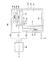
以下、図面を参照して本発明の望ましい一実施例をより詳細に説明する。図1は本発明の一実施例による液晶表示装置を示すブロック図である。 Hereinafter, a preferred embodiment of the present invention will be described in detail with reference to the drawings. FIG. 1 is a block diagram showing a liquid crystal display device according to an embodiment of the present invention.
図1に示すように、本発明の一実施例による液晶表示装置600はゲート駆動部200、データ駆動部300及びライン選択部400によって駆動されて映像を表示する液晶表示パネル100を含む。
As shown in FIG. 1, a liquid
コントローラー500は外部から提供される各種信号に応答して、前記ゲート駆動部200の駆動を制御する水平制御信号HCS、前記データ駆動部300の駆動を制御する垂直制御信号VCS及び前記ライン選択部400の動作を制御する選択制御信号TGを出力する。
The
前記液晶表示パネル100は第1基板、前記第1基板と向き合う第2基板及び前記第1基板と第2基板との間に介在された液晶層(図示せず)で構成され、映像を表示する表示領域DA、前記表示領域DAに隣接する第1及び第2周辺領域SA1、SA2に区分される。
The liquid
前記表示領域DAには、第1方向D1に延長された第1乃至第nゲートラインからなるゲートラインGL1〜GLn及び前記第1方向D1と直交する第2方向D2に延長された第1乃至第2mデータラインからなるデータラインDL1〜DL2mが具備される。ここで、mとnは1以上の自然数である。前記ゲートラインGL1〜GLnとデータラインDL1〜DL2mによって区画された2m×n個のそれぞれの画素領域にはTFT110及び画素電極120が具備される。
The display area DA includes gate lines GL1 to GLn including first to nth gate lines extending in a first direction D1 and first to first directions extending in a second direction D2 orthogonal to the first direction D1. Data lines DL1 to DL2m including 2m data lines are provided. Here, m and n are natural numbers of 1 or more. A
図1に示されたように、前記TFT110のゲート電極は前記ゲートラインのうち、一つのゲートラインGL1に連結され、ソース電極は前記データラインのうち一つのデータラインDL1に連結され、ドレーン電極は画素電極120と結合する。
As shown in FIG. 1, the gate electrode of the
前記第1周辺領域SA1は前記ゲートラインGL1〜GLnの一端部と隣接する領域であり、前記第1周辺領域SA1には前記ゲート駆動部200が前記表示領域DAに形成される。ゲート駆動部200は、前記TFT110を形成する工程を通じて共に形成される。前記ゲート駆動部200は前記第1ゲートラインGL1から順次に前記第nゲートラインGLnまでスキャン信号を出力する。
The first peripheral area SA1 is an area adjacent to one end of the gate lines GL1 to GLn, and the
前記第2周辺領域SA2は前記データラインDL1〜DL2mの一端部と隣接する領域であり、前記第2周辺領域SA2には前記データ駆動部300とライン選択部400とが具備される。例えば、前記データ駆動部300はチップ形態で前記第2周辺領域SA2に実装され、前記ライン選択部400は前記表示領域DAに形成される。前記ライン選択部400は、前記TFT110を形成する工程を通じて共に形成される。
The second peripheral area SA2 is an area adjacent to one end of the data lines DL1 to DL2m. The second peripheral area SA2 includes the
図2は図1に示されたライン選択部を具体的に示す図面である。図2に示すように、表示領域DAに具備されたデータラインDL1〜DL2mは、2m個のデータラインのうち一部であるm個のデータDL1〜DL2m−1からなる第1ラインブロックLB1と、残りのm個のデータラインDL2〜DL2mからなる第2ラインブロックLB2に区分される。例えば、前記第1ラインブロックLB1は奇数番目のデータラインからなり、前記第2ラインブロックLB2は偶数番目のデータラインからなる。 FIG. 2 is a diagram specifically showing the line selection unit shown in FIG. As shown in FIG. 2, the data lines DL1 to DL2m provided in the display area DA include a first line block LB1 including m pieces of data DL1 to DL2m−1 that are a part of 2m data lines, and The second line block LB2 is divided into the remaining m data lines DL2 to DL2m. For example, the first line block LB1 includes odd-numbered data lines, and the second line block LB2 includes even-numbered data lines.
前記データ駆動部300は、m個のチャンネル端子CH1〜CHmを通じてブロック単位でデータ信号を出力する。前記ライン選択部400は、前記第1ラインブロックLB1に連結された第1選択ブロックSB1及び前記第2ラインブロックLB2に連結された第2選択ブロックSB2からなり、前記データ駆動部300からブロック単位で出力されたデータ信号を第1及び第2ラインブロックLB1、LB2に時間差をおいて印加する。
The
前記第1選択ブロックSB1は、チャンネル端子CH1〜CHmと前記第1ラインブロックLB1との間に具備され、前記データ駆動部300から提供される第1選択信号TG1に応答して前記第1ラインブロックLB1に前記データ信号を出力する。また、前記第2選択ブロックSB2は、前記チャンネル端子CH1〜CHmと前記第2ラインブロックLB2との間に具備され、前記データ駆動部300から提供される第2選択信号TG2に応答して前記第2ラインブロックLB2に前記データ信号を出力する。
The first selection block SB1 is provided between the channel terminals CH1 to CHm and the first line block LB1 and is responsive to a first selection signal TG1 provided from the
例えば、前記第1及び第2選択信号TG1、TG2は互いに反転された位相を有し、その結果、前記第1及び第2選択ブロックSB1、SB2は互いに交互にターンオンされる。これにより、前記ライン選択部400は前記データ信号を前記第1ラインブロックLB1と第2ラインブロックLB2に交互に印加することができる。
For example, the first and second selection signals TG1 and TG2 have inverted phases, and as a result, the first and second selection blocks SB1 and SB2 are alternately turned on. Accordingly, the
前記第1選択ブロックSB1は、複数の第1選択スイッチング素子SW1を含み、前記第2選択ブロックSB2は複数の第2選択スイッチング素子SW2を含む。例えば、第1及び第2選択スイッチング素子はトランジスタである。図2に示されたように、前記第1選択スイッチング素子SW1のゲート電極は前記データ駆動部300から第1選択信号TG1を受信し、ソース電極は前記データ駆動部300からデータ信号を受信し、ドレイン電極は前記第1ラインブロックLB1に属する奇数番目のデータラインDL1〜DL2m−1に前記データ信号を出力する。
The first selection block SB1 includes a plurality of first selection switching elements SW1, and the second selection block SB2 includes a plurality of second selection switching elements SW2. For example, the first and second selection switching elements are transistors. As shown in FIG. 2, the gate electrode of the first selection switching element SW1 receives a first selection signal TG1 from the
一方、前記各第2選択スイッチング素子SW2のゲート電極は、前記データ駆動部300から第2選択信号TG2を受信し、ソース電極はデータ駆動部300からデータ信号を受信し、前記ドレイン電極は前記第2ラインブロックLB2に属する偶数番目のデータラインDL2〜DL2mに前記データ信号を出力する。
Meanwhile, the gate electrode of each of the second selection switching elements SW2 receives a second selection signal TG2 from the
図2では、前記データラインDL1〜DL2mに前記データ駆動部300のm個のチャンネル端子CH1〜CHmより2倍多い2m個のデータラインからなる実施例を示した。しかし、前記データラインは、前記m個のチャンネル端子より3倍、4倍、....多い3m、4m、...個のデータラインからなることができる。このとき、前記ライン選択部300は、3個、4個、...のブロックに分離された前記データラインにブロック単位で前記データ信号を印加する。
FIG. 2 illustrates an embodiment in which the data lines DL1 to DL2m include 2m data lines that are twice as many as the m channel terminals CH1 to CHm of the
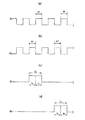
図3〜図4は図1に示されたゲート駆動部の出力による第1及び第2選択信号の位相を示す波形図である。特に、図3(b)及び図3(c)は、それぞれn個のゲートラインのうち奇数番目の第1及び第3ゲートラインの出力波形を示し、図4(b)及び図4(c)は、n個のゲートラインのうち偶数番目の第2及び第4ゲートラインの出力波形を示す。 3 to 4 are waveform diagrams showing the phases of the first and second selection signals according to the output of the gate driving unit shown in FIG. In particular, FIG. 3B and FIG. 3C show output waveforms of odd-numbered first and third gate lines of n gate lines, respectively, and FIG. 4B and FIG. 4C. Indicates the output waveforms of the even-numbered second and fourth gate lines out of n gate lines.
図3(a)乃至図3(d)に示すように、第1ゲートラインGL1にスキャン信号が印加されると、第1及び第2選択信号TG1、TG2は交互にハイレベルを有する。例えば、前記第1ゲートラインGL1にスキャン信号が印加される第1アクティブ区間T1は、前記第1選択信号TG1がハイレベルを有する第1選択区間t1及び前記第2選択信号TG2がハイレベルを有する第2選択区間t2で構成される。例えば、前記第1及び第2選択区間t1、t2は前記第1アクティブ区間T1の1/2である。 As shown in FIGS. 3A to 3D, when a scan signal is applied to the first gate line GL1, the first and second selection signals TG1 and TG2 alternately have a high level. For example, in a first active period T1 in which a scan signal is applied to the first gate line GL1, the first selection period t1 in which the first selection signal TG1 has a high level and the second selection signal TG2 have a high level. It is comprised by the 2nd selection area t2. For example, the first and second selection sections t1 and t2 are ½ of the first active section T1.
また、例えば、第3ゲートラインGL3にスキャン信号が印加される第3アクティブ区間T3は、前記第1選択信号TG1がハイレベルを有する第5選択区間t5と前記第2選択信号TG2がハイレベルを有する第6選択区間t6とで構成される。例えば、前記第5及び第6選択区間t5、t6は前記第3アクティブ区間T3の1/2である。 For example, in the third active period T3 in which the scan signal is applied to the third gate line GL3, the fifth selection period t5 in which the first selection signal TG1 has a high level and the second selection signal TG2 have a high level. And a sixth selection section t6. For example, the fifth and sixth selection intervals t5 and t6 are ½ of the third active interval T3.
一方、図4(a)ないし図4(d)に示されたように、例えば、第2ゲートラインGL2にスキャン信号が印加される第2アクティブ区間T2は、前記第2選択信号TG2がハイレベルを有する第3選択区間t3と前記第1選択信号TG1がハイレベルを有する第4選択区間t4とで構成される。 On the other hand, as shown in FIGS. 4A to 4D, for example, in the second active period T2 in which the scan signal is applied to the second gate line GL2, the second selection signal TG2 is at a high level. And a fourth selection section t4 in which the first selection signal TG1 has a high level.
また、例えば第4ゲートラインGL4にスキャン信号が印加される第4アクティブ区間T4は、前記第2選択信号TG2がハイレベルを有する第7選択区間t7と前記第1選択信号TG1がハイレベルを有する第8選択区間t8とで構成される。 For example, in the fourth active period T4 in which the scan signal is applied to the fourth gate line GL4, the seventh selection period t7 in which the second selection signal TG2 has a high level and the first selection signal TG1 have a high level. It is comprised with the 8th selection area t8.
このように、奇数番目のゲートラインGL1、GL3のアクティブ区間T1、T3では、前記第1選択信号TG1に応答して前記第1選択ブロックSB1がまずターンオンされ、その後、前記第2選択信号TG2に応答して前記第2選択ブロックSB2がターンオンされる。偶数番目のゲートラインGL2、GL4のアクティブ区間T2、T4では、前記第2選択信号TG2に応答して前記第2選択ブロックSB2がまずターンオンされ、その後、前記第1選択信号TG1に応答して前記第1選択ブロックSB1がターンオンされる。 As described above, in the active periods T1 and T3 of the odd-numbered gate lines GL1 and GL3, the first selection block SB1 is first turned on in response to the first selection signal TG1, and then the second selection signal TG2 is applied. In response, the second selection block SB2 is turned on. In the active periods T2 and T4 of the even-numbered gate lines GL2 and GL4, the second selection block SB2 is first turned on in response to the second selection signal TG2, and then in response to the first selection signal TG1. The first selection block SB1 is turned on.
また、これとは反対に、奇数番目のゲートラインGL1、GL3のアクティブ区間T1、T3では、前記第2選択信号TG2に応答して前記第2選択ブロックSB2がターンオンされ、その後、前記第1選択信号TG1に応答して前記第1選択ブロックSB1がターンオンされることもできる。そして、偶数番目のゲートラインGL2、GL4のアクティブ区間T2、T4では前記第1選択信号TG1に応答して前記第1選択ブロックSB1がまずターンオンされ、その後、前記第2選択信号TG2に応答して前記第2選択ブロックSB2がターンオンされることもできる。 In contrast, in the active periods T1 and T3 of the odd-numbered gate lines GL1 and GL3, the second selection block SB2 is turned on in response to the second selection signal TG2, and then the first selection is performed. The first selection block SB1 may be turned on in response to the signal TG1. In the active periods T2 and T4 of the even-numbered gate lines GL2 and GL4, the first selection block SB1 is first turned on in response to the first selection signal TG1, and then in response to the second selection signal TG2. The second selection block SB2 may be turned on.
従って、前記第1乃至第4アクティブ区間T1〜T4において、前記第1及び第2ラインブロックLB1、LB2に時間差を置いてデータ信号をそれぞれ印加することができる。前記第1及び第2ラインブロックLB1、LB2が選択される順序はゲートライン単位で異なる。 Therefore, in the first to fourth active periods T1 to T4, data signals can be applied to the first and second line blocks LB1 and LB2 with a time difference. The order in which the first and second line blocks LB1 and LB2 are selected is different for each gate line.
図5(a)乃至図5(d)は、奇数番目のフレームでの時間の流れによるライン選択部の出力波形図であり、図6は液晶表示パネルの画素領域別データ信号の極性を示す図面である。ここで、1フレームは一番目のゲートラインからn番目のゲートラインまで順次にスキャン信号が印加される間の時間区間として定義される。また、1フレームは一番目のゲートラインから最後のゲートラインまで順次にアクティブされる間の時間区間として定義することができる。例えば、フレームが1秒に64回変わる場合、奇数フレームは64個のフレームのうち、奇数番目のフレームを示す。 FIGS. 5A to 5D are output waveform diagrams of the line selection unit according to the flow of time in odd-numbered frames, and FIG. 6 is a diagram illustrating the polarity of the data signal for each pixel area of the liquid crystal display panel. It is. Here, one frame is defined as a time interval during which scan signals are sequentially applied from the first gate line to the nth gate line. One frame can be defined as a time interval during which the first gate line is sequentially activated from the first gate line. For example, when the frame changes 64 times per second, the odd frame indicates an odd-numbered frame among the 64 frames.
但し、図5(a)乃至図5(d)では、例えば、n個のゲートラインのうち第1乃至第4ゲートラインGL1〜GL4を示し、2m個のデータラインのうち第1乃至第10データラインDL1〜DL10のみを示す。 However, in FIGS. 5A to 5D, for example, the first to fourth gate lines GL1 to GL4 among n gate lines are shown, and the first to tenth data among 2m data lines are shown. Only lines DL1-DL10 are shown.
図5(a)で実線は第1ラインブロックのデータラインに印加される第1データ信号を示し、点線は第2ラインブロックのデータラインに印加される第2データ信号を示す。 In FIG. 5A, the solid line indicates the first data signal applied to the data line of the first line block, and the dotted line indicates the second data signal applied to the data line of the second line block.
また、図15で斜線部分は相対的に明るい画素領域603、605を示し、斜線のない部分は相対的に暗い画素領域601を示す。 In FIG. 15, shaded portions indicate relatively bright pixel regions 603 and 605, and portions without hatched portions indicate relatively dark pixel regions 601.
図5乃至図6に示すように、第1ゲートラインGL1には第1アクティブ区間(T1、図3(a)に図示)の間スキャン信号が出力される。このとき、前記第1アクティブ区間T1の一部である第1選択区間t1で第1ラインブロック(LB1、図2に図示)に第1データ信号が印加され、前記第1アクティブ区間T1の残りの第2選択区間t2で第2ラインブロック(LB2、図2に図示)に前記第2データ信号が印加される。 As shown in FIGS. 5 to 6, a scan signal is output to the first gate line GL1 during the first active period (T1, shown in FIG. 3A). At this time, the first data signal is applied to the first line block (LB1, shown in FIG. 2) in the first selection period t1, which is a part of the first active period T1, and the remaining part of the first active period T1. In the second selection period t2, the second data signal is applied to the second line block (LB2, shown in FIG. 2).
前記第1選択区間t1でハイレベルを有する第1選択信号(TG1、図3(a)に図示)に応答して前記第1ラインブロックLB1に前記第1データ信号が出力され、前記第2選択区間t2でハイレベルを有する第2選択信号(TG2、図3(b)に図示)に応答して前記第2ラインブロックLB2に前記第2データ信号が出力される。 In response to a first selection signal (TG1, shown in FIG. 3A) having a high level in the first selection period t1, the first data signal is output to the first line block LB1, and the second selection signal is output. The second data signal is output to the second line block LB2 in response to a second selection signal (TG2, shown in FIG. 3B) having a high level in the section t2.
即ち、全体ゲートラインのうち奇数番目のゲートラインGL1、GL3が駆動されると、全体データラインのうちまず、奇数番目のデータラインにデータ信号が出力され、その後、偶数番目のデータラインにデータ信号が出力される。 That is, when the odd-numbered gate lines GL1 and GL3 among the entire gate lines are driven, the data signal is first output to the odd-numbered data lines of the entire data lines, and then the data signals are output to the even-numbered data lines. Is output.
反面、偶数番目のゲートラインGL2、GL4が駆動されると、全体のデータラインのうち、まず、偶数番目のデータラインにデータ信号が出力され、その後、奇数番目のデータラインにデータ信号が出力される。 On the other hand, when the even-numbered gate lines GL2 and GL4 are driven, the data signal is first output to the even-numbered data line among the entire data lines, and then the data signal is output to the odd-numbered data line. The
例えば、前記第1及び第2データ信号の正極性+は、共通電圧Vcomより高い電位を有し、前記第1及び第2データ信号の負極性−は前記共通電圧より低い電位を有する。 For example, the positive polarity + of the first and second data signals has a higher potential than the common voltage Vcom, and the negative polarity of the first and second data signals has a lower potential than the common voltage.
例えば、図6に示すように、前記第1選択区間t1の間、第1、第5及び第9データラインDL1、DL5、DL9には正極性+の第1データ信号が印加され、第3及び第7データラインDL3、DL7には負極性−の第1データ信号が印加される。また、例えば、前記第2選択区間t2の間、第2、第6及び第10データラインDL2、DL6、DL10には正極性+の第2データ信号が印加され、第4及び第8データラインDL4、DL8には負極性−の第2データ信号が印加される。 For example, as shown in FIG. 6, during the first selection period t1, the first data signal having positive polarity is applied to the first, fifth, and ninth data lines DL1, DL5, and DL9, A negative first data signal is applied to the seventh data lines DL3 and DL7. Further, for example, during the second selection period t2, the second data signal having positive polarity + is applied to the second, sixth, and tenth data lines DL2, DL6, and DL10, and the fourth and eighth data lines DL4 are applied. , DL8 is applied with the negative second data signal.
前記第1アクティブ区間T1内で前記第1ラインブロックLB1に印加される前記第1データ信号は、前記第2ラインブロックLB2に印加される前記第2データ信号と同一の極性を有する。 The first data signal applied to the first line block LB1 within the first active period T1 has the same polarity as the second data signal applied to the second line block LB2.
以後、第2ゲートラインGL2には第2アクティブ区間(T2、図4(c)に図示)の間前記スキャン信号が印加され、前記第2アクティブ区間T2の一部である第3選択区間t3には前記第2ラインブロックLB2に前記第2データ信号が印加される。また、前記第2アクティブ区間T2の残りの一部である第4選択区間t4で前記第1ラインブロックLB1に前記第1データ信号が印加される。 Thereafter, the scan signal is applied to the second gate line GL2 during a second active period (T2, shown in FIG. 4C), and the second selection period t3, which is a part of the second active period T2, is applied. The second data signal is applied to the second line block LB2. In addition, the first data signal is applied to the first line block LB1 in the fourth selection period t4 which is the remaining part of the second active period T2.
例えば、前記第3選択区間t3の間前記第2、第6及び第10データラインDL2、DL6、DL10には負極性−の第2データ信号が印加され、前記第4及び第8データラインDL4、DL8には正極性+の第2データ信号が印加される。また、例えば、前記第4選択区間t4の間前記第1、第5及び第9データラインDL1、DL5、DL9には正極性+の第1データ信号が印加され、前記第3及び第7データラインDL3、DL7には負極性−の第1データ信号が印加される。 For example, a second negative data signal is applied to the second, sixth, and tenth data lines DL2, DL6, and DL10 during the third selection period t3, and the fourth and eighth data lines DL4, DL4, A positive second data signal is applied to DL8. Also, for example, a positive first data signal is applied to the first, fifth, and ninth data lines DL1, DL5, DL9 during the fourth selection period t4, and the third and seventh data lines are applied. A negative first data signal is applied to DL3 and DL7.
前記第2アクティブ区間T2で、前記第1及び第2データ信号の極性は、前記第1アクティブ区間T1から出力された前記第1及び第2データ信号の極性が、図6の第3方向D3に1個の画素領域分だけシフトされるのと同一である。即ち、前記第1アクティブ区間T1で前記第2ラインブロックLB2に印加された第2データ信号が、前記第2アクティブ区間T2で第1データ信号として前記第1ブロックLB1に印加される。従って、前記第2アクティブ区間T2内で前記第1ラインブロックLB1に印加される前記第1データ信号は、前記第2ラインブロックLB2に印加される前記第2データ信号と互いに異なる極性を有する。 In the second active period T2, the polarities of the first and second data signals are the same as the polarities of the first and second data signals output from the first active period T1 in the third direction D3 of FIG. This is the same as shifting by one pixel area. That is, the second data signal applied to the second line block LB2 in the first active period T1 is applied to the first block LB1 as the first data signal in the second active period T2. Accordingly, the first data signal applied to the first line block LB1 within the second active period T2 has a polarity different from that of the second data signal applied to the second line block LB2.
以後、第3ゲートラインGL3に第3アクティブ区間(T3、図4(d)に示す)の間、前記スキャン信号が印加され、前記第3アクティブ区間T3の一部である第5選択区間t5では第1ラインブロックLB1に第1データ信号が印加される。また、前記第3アクティブ区間T3の残りの一部である第6選択区間t6では第2ラインブロックLB2に前記第2データ信号が印加される。 Thereafter, the scan signal is applied to the third gate line GL3 during a third active period (T3, shown in FIG. 4D), and in a fifth selection period t5 that is a part of the third active period T3. A first data signal is applied to the first line block LB1. In addition, the second data signal is applied to the second line block LB2 in the sixth selection period t6 which is the remaining part of the third active period T3.
例えば、前記第5選択区間t5の間、前記第1、第5及び第9データラインDL1、DL5、DL9には負極性−の第1データ信号が印加され、前記第3及び第7データラインDL3、DL7には正極性+の第1データ信号が印加される。また、例えば、前記第6選択区間t6の間前記第2、第6及び第10データライン(DL2、DL6、DL10)には負極性−の第2データ信号が印加され、前記第4及び第8データラインDL4〜DL8には正極性+の第2データ信号が印加される。 For example, a negative first data signal is applied to the first, fifth, and ninth data lines DL1, DL5, and DL9 during the fifth selection period t5, and the third and seventh data lines DL3 are applied. , DL7 is applied with a positive first data signal. In addition, for example, during the sixth selection period t6, the second, sixth, and tenth data lines (DL2, DL6, DL10) are applied with the negative second data signal, and the fourth and eighth data lines are applied. A positive second data signal is applied to the data lines DL4 to DL8.
前記第3アクティブ区間T3で前記第1及び第2データ信号の極性は前記第2アクティブ区間T2から出力された前記第1及び第2データ信号の極性が図6の前記第3方向D3に1個の画素領域分だけシフトされたのと同一である。従って、前記第3アクティブ区間T3内で前記第1ラインブロックLB1に印加される前記第1データ信号は前記第2ラインブロックLB2に印加される前記第2データ信号と同一の極性を有する。 The polarity of the first and second data signals in the third active period T3 is one in the third direction D3 of FIG. 6 in the polarity of the first and second data signals output from the second active period T2. It is the same as that shifted by the pixel area. Accordingly, the first data signal applied to the first line block LB1 within the third active period T3 has the same polarity as the second data signal applied to the second line block LB2.
第4アクティブ区間T4の間、第4ゲートラインGL4に前記スキャン信号が印加され、前記第4アクティブ区間T4の一部である第7選択区間t7には第2ラインブロックLB2に第2データ信号が印加される。また、前記第4アクティブ区間T4の残りの一部である第8選択区間t8には第1ラインブロックLB1に前記第1データ信号が印加される。 During the fourth active period T4, the scan signal is applied to the fourth gate line GL4. In the seventh selection period t7, which is a part of the fourth active period T4, the second data signal is transmitted to the second line block LB2. Applied. The first data signal is applied to the first line block LB1 during the eighth selection period t8, which is the remaining part of the fourth active period T4.
例えば、前記第7選択区間t7の間前記第2、第6及び第10データラインDL2、DL6、DL10には正極性+の第2データ信号が印加され、前記第4及び第8データラインDL4、DL8には負極性−の第2データ信号が印加される。また、例えば、前記第8選択区間t8の間前記第1、第5及び第9データラインDL1、DL5、DL9には負極性−の第1データ信号が印加され、前記第3及び第7データラインDL3、DL7には正極性+の第1データ信号が印加される。 For example, a positive second data signal is applied to the second, sixth, and tenth data lines DL2, DL6, and DL10 during the seventh selection period t7, and the fourth and eighth data lines DL4, A second data signal having a negative polarity is applied to DL8. For example, a negative first data signal is applied to the first, fifth, and ninth data lines DL1, DL5, and DL9 during the eighth selection period t8, and the third and seventh data lines are applied. A positive first data signal is applied to DL3 and DL7.
前記第4アクティブ区間T4で前記第1及び第2データ信号の極性は前記第3アクティブ区間T3から出力された前記第1及び第2データ信号の極性が図6の第3方向D3に1個の画素領域分だけシフトされたのと同一である。従って、前記第4アクティブ区間T4内で前記第1ラインブロックLB1に印加される前記第1データ信号は前記第2ラインブロックLB2に印加される前記第2データ信号と互いに異なる極性を有する。 In the fourth active period T4, the polarities of the first and second data signals are one in the third direction D3 of FIG. 6 in the polarity of the first and second data signals output from the third active period T3. It is the same as that shifted by the pixel area. Accordingly, the first data signal applied to the first line block LB1 in the fourth active period T4 has a polarity different from that of the second data signal applied to the second line block LB2.
図5(a)乃至図5(d)に示されたように、液晶表示装置に信号を印加することで、液晶表示装置の画面上に相対的に明るい画素領域603、605と相対的に暗い画素領域601に交互に示されるようになる。これにより、明るい画素領域と暗い画素領域との混合を通じて前記液晶表示装置の画面の全体的な輝度は同一になる。 As shown in FIGS. 5A to 5D, by applying a signal to the liquid crystal display device, relatively bright pixel regions 603 and 605 and relatively dark on the screen of the liquid crystal display device. The pixel regions 601 are alternately shown. Accordingly, the overall luminance of the screen of the liquid crystal display device is the same through the mixture of the bright pixel region and the dark pixel region.
図7(a)乃至図7(d)は偶数番目フレームでの時間流れによるライン選択部400の出力波形図であり、図20は画素領域別データ信号の極性を示す図面である。ここで、偶数フレームは64個のうち偶数番目のフレームで定義される。
FIGS. 7A to 7D are output waveform diagrams of the
また、図7(a)乃至図7(d)で実線は第1ラインブロックのデータラインに印加される第1データ信号を示し、点線は第2ラインブロックのデータラインに印加される第2データ信号を示す。 7A to 7D, the solid line indicates the first data signal applied to the data line of the first line block, and the dotted line indicates the second data applied to the data line of the second line block. Signals are shown.
また、図8で斜線部分は相対的に明るい画素領域803、805を示し、斜線のない部分は相対的に暗い画素領域801を示す。
In FIG. 8, shaded portions indicate relatively
図7(a)乃至図7(d)に示すように、例えば、第1ゲートラインGL1にスキャン信号が印加される第1アクティブ区間T1のうち第1選択区間t1の間第1、第5及び第9データラインDL1、DL5、DL9には負極性−の第1データ信号が印加され、第3及び第7データラインDL3、DL7には正極性+の第1データ信号が印加される。以後、例えば、第2選択区間t2の間第2、第6及び第10データラインDL2、DL6、DL10には負極性−の第2データ信号が印加され、第4及び第8データラインDL4、DL8には正極性+の第2データ信号が印加される。 As shown in FIGS. 7A to 7D, for example, the first, fifth, and first periods of the first selection period t1 in the first active period T1 in which the scan signal is applied to the first gate line GL1. A negative first data signal is applied to the ninth data lines DL1, DL5, DL9, and a positive first data signal is applied to the third and seventh data lines DL3, DL7. Thereafter, for example, during the second selection period t2, the negative second data signal is applied to the second, sixth, and tenth data lines DL2, DL6, and DL10, and the fourth and eighth data lines DL4, DL8 are applied. The positive second data signal is applied to.
例えば、第2ゲートラインDL2にスキャン信号が印加される第2アクティブ区間T2のうち、第3選択区間t3の間前、記第2、第6及び第10データラインDL2、DL6、DL10には正極性+の第1データ信号が印加され、前記第4及び第8データラインDL4、DL8には負極性−の第1データ信号が印加される。以後、例えば、第4選択区間t4の間前記第1、第5及び第9データラインDL1、DL5、DL9には負極性−の第2データ信号が印加され、前記第3及び第7データラインDL3、DL7には正極性+の第2データ信号が印加される。 For example, the second, sixth, and tenth data lines DL2, DL6, and DL10 have a positive polarity before the third selection period t3 in the second active period T2 in which the scan signal is applied to the second gate line DL2. The first data signal having a positive polarity is applied, and the first data signal having a negative polarity is applied to the fourth and eighth data lines DL4 and DL8. Thereafter, for example, a negative second data signal is applied to the first, fifth, and ninth data lines DL1, DL5, and DL9 during the fourth selection period t4, and the third and seventh data lines DL3 are applied. , A positive second data signal is applied to DL7.
例えば、第3ゲートラインGL3にスキャン信号が印加される第3アクティブ区間T3のうち、第5選択区間t5の間前記第1、第5及び第9データラインDL1、DL5、DL9には正極性+の第1データ信号が印加され、前記第3及び第7データラインDL3、DL7には負極性−の第1データ信号が印加される。以後、例えば、第6選択区間t6の間前記第2、第6及び第10データラインDL2、DL6、DL10には正極性+の第2データ信号が印加され、前記第4及び第8データラインDL4、DL8には負極性−の第2データ信号が印加される。 For example, in the third active period T3 in which the scan signal is applied to the third gate line GL3, the first, fifth, and ninth data lines DL1, DL5, and DL9 are positive in the fifth selection period t5. The first data signal is applied, and the negative first data signal is applied to the third and seventh data lines DL3 and DL7. Thereafter, for example, during the sixth selection period t6, a positive second data signal is applied to the second, sixth, and tenth data lines DL2, DL6, and DL10, and the fourth and eighth data lines DL4. , DL8 is applied with the negative second data signal.
例えば、第4ゲートラインGL4にスキャン信号が印加される第4アクティブ区間T4のうち、第7選択区間t7の間前記第2、第6及び第10データラインDL2、DL6、DL10には正極性+の第2データ信号が印加され、前記第4及び第8データラインDL4、DL8には負極性−の第2データ信号が印加される。以後、第8選択区間t8の間前記第1、第5及び第9データラインDL1、DL5、DL9には負極性−の第1データ信号が印加され、前記第3及び第7データラインDL3、DL7には正極性+の第1データライン信号が印加される。 For example, in the fourth active period T4 in which the scan signal is applied to the fourth gate line GL4, the second, sixth, and tenth data lines DL2, DL6, and DL10 have a positive polarity during the seventh selection period t7. The second data signal is applied, and a negative second data signal is applied to the fourth and eighth data lines DL4 and DL8. Thereafter, a negative first data signal is applied to the first, fifth, and ninth data lines DL1, DL5, and DL9 during an eighth selection period t8, and the third and seventh data lines DL3, DL7 are applied. A positive first data line signal is applied to.
このように、液晶表示装置の画面上に相対的に明るい画素領域803、805と暗い画素領域801とが交互的に示されることで、明るい画素領域803、805と暗い画素領域801との混合を通じて前記画面の全体的な輝度は同一になる。
As described above, the relatively
図5乃至図7に示されたように、奇数フレームで画素領域に印加されるデータ信号の極性と偶数フレームで画素領域に印加されるデータ信号の極性とが互いに異なる。しかし、奇数フレームで相対的に明るく示される画素領域603、605が偶数フレームでも相対的に明るい画素領域803、805として示されることで、フレームが変わっても液晶表示装置の画面は全体的に均一な輝度を有することができる。
As shown in FIGS. 5 to 7, the polarity of the data signal applied to the pixel area in the odd frame and the polarity of the data signal applied to the pixel area in the even frame are different from each other. However, since the pixel areas 603 and 605 that are relatively bright in the odd frame are displayed as the relatively
図2乃至図8では液晶表示パネルに具備されるデータラインの個数がデータ駆動部の出力端子の2倍として、データラインが2つのブロックに分割される場合を示した。しかし、液晶表示パネルの解像度の増加に起因して前記データラインは前記出力端子の3倍、4倍またはその以上に構成されることができる。 2 to 8 show a case where the number of data lines provided in the liquid crystal display panel is twice the number of output terminals of the data driver, and the data lines are divided into two blocks. However, due to the increase in resolution of the liquid crystal display panel, the data line can be configured to be three times, four times or more than the output terminal.
このような液晶表示装置及びこれの駆動方法によると、データ駆動部はアクティブ区間の間、m/i個のデータ信号をi回出力するものの、アクティブ区間単位でデータ信号の極性をシフトさせて出力する。ライン選択部は各ブロックにm/i個のデータ信号を印加し、ゲートライン単位で各ブロックが選択される時間を異なるようにする。 According to the liquid crystal display device and the driving method thereof, the data driver outputs m / i data signals i times during the active period, but outputs the data signal by shifting the polarity of the data signal in units of the active period. To do. The line selection unit applies m / i data signals to each block so that the time for selecting each block is different for each gate line.
従って、液晶表示装置の画面上に相対的に明るい画素領域とくらい画素領域とが交互的に示されることで、明るい画素領域と暗い画素領域との混合を通じて全体的な輝度は同一になる。これにより、液晶表示装置の表示特性を向上させることができる。 Accordingly, the relatively bright pixel areas and the pixel areas are alternately shown on the screen of the liquid crystal display device, so that the overall luminance becomes the same through the mixture of the bright pixel areas and the dark pixel areas. Thereby, the display characteristic of a liquid crystal display device can be improved.
以上、本発明の実施例によって詳細に説明したが、本発明はこれに限定されず、本発明が属する技術分野において通常の知識を有する者であれば、本発明の思想と精神を離れることなく、本発明を修正または変更できる。 As described above, the embodiments of the present invention have been described in detail. However, the present invention is not limited thereto, and those who have ordinary knowledge in the technical field to which the present invention belongs can be used without departing from the spirit and spirit of the present invention. The present invention can be modified or changed.
(b)図1に示されたゲート駆動部の出力による第1及び第2選択信号の位相を示す波形図である。 FIG. 4B is a waveform diagram illustrating phases of first and second selection signals based on an output of the gate driving unit illustrated in FIG. 1.
(c)それぞれn個のゲートラインのうち第1及び第3ゲートラインの出力波形を示す波形図である。 (C) It is a wave form diagram which shows the output waveform of the 1st and 3rd gate line among n gate lines, respectively.
(d)それぞれn個のゲートラインのうち第1及び第3ゲートラインの出力波形を示す波形図である。
(b)図1に示されたゲート駆動部の出力による第1及び第2選択信号の位相を示す波形図である。 FIG. 4B is a waveform diagram illustrating phases of first and second selection signals based on an output of the gate driving unit illustrated in FIG. 1.
(c)n個のゲートラインのうち、第2及び第4ゲートラインの出力波形を示す波形図である。 (C) It is a wave form diagram which shows the output waveform of the 2nd and 4th gate line among n gate lines.
(d)n個のゲートラインのうち、第2及び第4ゲートラインの出力波形を示す波形図である。
(b)奇数フレームで時間の流れによるライン選択部の出力波形図である。 (B) It is an output waveform figure of the line selection part by the flow of time in odd-numbered frames.
(c)奇数フレームで時間の流れによるライン選択部の出力波形図である。 (C) It is an output waveform diagram of the line selection unit according to the flow of time in odd frames.
(d)奇数フレームで時間の流れによるライン選択部の出力波形図である。
(b)偶数フレームで時間の流れによるライン選択部の出力波形図である。 (B) It is an output waveform figure of the line selection part by the flow of time in an even-numbered frame.
(c)偶数フレームで時間の流れによるライン選択部の出力波形図である。 (C) It is an output waveform diagram of the line selection unit according to the flow of time in even frames.
(d)偶数フレームで時間の流れによるライン選択部の出力波形図である。
100 液晶表示パネル
110 TFT
120 画素電極
200 ゲート駆動部
300 データ駆動部
400 ライン選択部
500 コントローラー
600 液晶表示装置
100
120 pixel electrode
200
Claims (26)
前記ゲートラインを順次にアクティブさせるスキャン信号を出力するゲート駆動部と、
前記ゲートラインがアクティブにされるアクティブ区間のあいだ、各ブロック単位で前記複数個のデータラインにデータ信号を出力し、二度の前記アクティブ区間経過の際に出力される前記データ信号の極性が反転された位相を有するようにデータ信号を出力するデータ駆動部と、
前記各ゲートライン毎に各ブロックが選択される時間を異なるようにして前記各ブロックに前記データ信号を印加するライン選択部と、
を含むことを特徴とする表示装置。 A display panel comprising a plurality of gate lines and a plurality of data lines separated into a plurality of blocks;
A gate driver for outputting a scan signal for sequentially activating the gate lines;
During the active period in which the gate line is activated, data signals are output to the plurality of data lines in units of blocks, and the polarity of the data signal output when the active period has passed twice is inverted. A data driver for outputting a data signal so as to have a phase that is
A line selection unit that applies the data signal to each of the blocks in a different time for each block to be selected for each of the gate lines;
A display device comprising:
ここで、mは偶数。 2. The display according to claim 1, wherein the number of the data lines is m, and the data line includes a first block composed of m / 2 data lines and a second block composed of the remaining m / 2 data lines. Device where m is an even number.
前記第1選択信号に応答して前記第1ブロックに前記データ信号を提供する第1選択部と、
第2選択信号に応答して前記第2ブロックに前記データ信号を提供する第2選択部と、
を含むことを特徴とする請求項2記載の表示装置。 The line selection unit
A first selector for providing the data signal to the first block in response to the first selection signal;
A second selector for providing the data signal to the second block in response to a second selection signal;
The display device according to claim 2, further comprising:
前記データ駆動部は現在フレームから各データラインに前記第1極性のデータ信号を印加すると、次のフレームから前記各データラインに前記第2極性のデータ信号を印加することを特徴とする請求項8記載の表示装置。 When defining the time interval during which the scan signal is sequentially applied from the first gate line to the last gate line as a frame,
9. The data driver according to claim 8, wherein when the data signal having the first polarity is applied to each data line from the current frame, the data signal having the second polarity is applied to each data line from the next frame. The display device described.
i番目のゲートラインをアクティブさせる段階と、
前記i番目のゲートラインにアクティブされた間、各ブロック単位でデータ信号を出力する段階と、
i+1番目のゲートラインをアクティブさせる段階と、
前記i+1番目のゲートラインにアクティブされた間、各ブロック単位でデータ信号を出力する段階と、
i+2番目のゲートラインをアクティブさせる段階と、
前記i+2番目のゲートラインにアクティブされた間、前記i番目のゲートラインがアクティブされた間各ブロック単位で印加されたデータ信号と反対の位相を有するデータ信号をブロック単位で出力する段階と、
を含むことを特徴とする表示装置駆動方法
ここで、m、nは2以上の自然数であり、iは(n−2)より小さいか同じの自然数。 In a method of driving a display device having a display panel having a plurality of data lines divided into a plurality of blocks each including n gate lines and m data lines,
activating the i-th gate line;
Outputting a data signal in units of blocks while the i-th gate line is activated;
activating the (i + 1) th gate line;
Outputting a data signal in units of blocks while being activated by the (i + 1) th gate line;
activating the i + 2nd gate line;
Outputting a data signal having a phase opposite to that applied to each block while the i-th gate line is activated while the i + 2 gate line is activated;
Here, m and n are natural numbers of 2 or more, and i is a natural number smaller than or equal to (n−2).
ここで、但し、mは偶数である。 13. The display device according to claim 12, wherein the data line includes a first block made up of m / 2 data lines and a second block made up of the remaining m / 2 data lines. Driving method Here, m is an even number.
第1グループのゲートラインがアクティブされると、第1ブロックのデータラインに第1データ信号を出力した後第2ブロックのデータラインに第2データ信号を出力する段階と、
第2グループのゲートラインがアクティブされると、前記第2ブロックのデータラインに第3データ信号を出力した後前記第1ブロックのデータラインに第4データ信号を出力する段階と、
を含む表示装置駆動方法。 In a method of driving a display device having a plurality of gate lines, a plurality of data lines divided into a plurality of blocks each including at least two data lines, and a display panel including a plurality of pixels,
When the first group of gate lines is activated, outputting the first data signal to the data line of the first block and then outputting the second data signal to the data line of the second block;
When a second group of gate lines is activated, outputting a third data signal to the data line of the second block and then outputting a fourth data signal to the data line of the first block;
A display device driving method including:
奇数番目のフレームに各画素に印加されるデータ信号の極性と偶数番目のフレームに前記各画素に印加されるデータ信号の極性とが互いに反対であることを特徴とする請求項17記載の表示装置駆動方法。 When defining the time interval between the first gate line and the last gate line sequentially activated as a frame,
18. The display device according to claim 17, wherein the polarity of the data signal applied to each pixel in the odd-numbered frame and the polarity of the data signal applied to each pixel in the even-numbered frame are opposite to each other. Driving method.
第1グループのゲートラインがアクティブされると、第1ブロックのデータラインに第1データ信号を出力した後第2ブロックのデータラインに第2データ信号を出力し、第2グループのゲートラインがアクティブされると、前記第2ブロックのデータラインに第3データ信号を出力した後前記第1ブロックのデータラインに第4データ信号を出力することを特徴とする表示装置の駆動装置。 An apparatus for driving a display device having a plurality of gate lines, a plurality of data lines divided into a plurality of blocks each including at least two data lines, and a display panel including a plurality of pixels,
When the first group of gate lines is activated, the first data signal is output to the data line of the first block, and then the second data signal is output to the data line of the second block, and the second group of gate lines is activated. Then, the third data signal is output to the data line of the second block, and then the fourth data signal is output to the data line of the first block.
Applications Claiming Priority (1)
| Application Number | Priority Date | Filing Date | Title |
|---|---|---|---|
| KR1020030071041A KR20050035385A (en) | 2003-10-13 | 2003-10-13 | Display apparatus and method of driving the same |
Publications (1)
| Publication Number | Publication Date |
|---|---|
| JP2005122172A true JP2005122172A (en) | 2005-05-12 |
Family
ID=34374262
Family Applications (1)
| Application Number | Title | Priority Date | Filing Date |
|---|---|---|---|
| JP2004298524A Withdrawn JP2005122172A (en) | 2003-10-13 | 2004-10-13 | Display apparatus and method and device for driving the same |
Country Status (5)
| Country | Link |
|---|---|
| US (1) | US20050078075A1 (en) |
| EP (1) | EP1524647A3 (en) |
| JP (1) | JP2005122172A (en) |
| KR (1) | KR20050035385A (en) |
| TW (1) | TW200532633A (en) |
Families Citing this family (8)
| Publication number | Priority date | Publication date | Assignee | Title |
|---|---|---|---|---|
| KR101253273B1 (en) * | 2005-12-16 | 2013-04-10 | 삼성디스플레이 주식회사 | Display apparatus and method for driving the same |
| KR20070115371A (en) * | 2006-06-02 | 2007-12-06 | 삼성전자주식회사 | Display device and driving apparatus and method driving thereof |
| US20080150862A1 (en) * | 2006-12-26 | 2008-06-26 | Sheng-Pin Tseng | Lcd device capable of reducing line flicker and horizontal crosstalk for rgbw subpixel arrangement |
| TW200933583A (en) * | 2008-01-30 | 2009-08-01 | Chunghwa Picture Tubes Ltd | Source driving circuit |
| TWI393107B (en) * | 2008-07-02 | 2013-04-11 | Au Optronics Corp | Liquid crystal display device |
| US11017709B2 (en) * | 2018-03-02 | 2021-05-25 | Xianyang Caihong Optoelectronics Technology Co., Ltd | Driving method for pixel matrix and display device |
| CN109032409B (en) * | 2018-07-26 | 2021-11-02 | 京东方科技集团股份有限公司 | Display panel driving method, display panel and display device |
| CN110648639B (en) * | 2019-09-27 | 2022-07-08 | 京东方科技集团股份有限公司 | Liquid crystal display and driving method and device thereof |
Family Cites Families (2)
| Publication number | Priority date | Publication date | Assignee | Title |
|---|---|---|---|---|
| JP4031291B2 (en) * | 2001-11-14 | 2008-01-09 | 東芝松下ディスプレイテクノロジー株式会社 | Liquid crystal display |
| JP3791452B2 (en) * | 2002-05-02 | 2006-06-28 | ソニー株式会社 | Display device, driving method thereof, and portable terminal device |
-
2003
- 2003-10-13 KR KR1020030071041A patent/KR20050035385A/en not_active Application Discontinuation
-
2004
- 2004-10-08 EP EP04256258A patent/EP1524647A3/en not_active Withdrawn
- 2004-10-12 US US10/961,190 patent/US20050078075A1/en not_active Abandoned
- 2004-10-13 TW TW093131032A patent/TW200532633A/en unknown
- 2004-10-13 JP JP2004298524A patent/JP2005122172A/en not_active Withdrawn
Also Published As
| Publication number | Publication date |
|---|---|
| KR20050035385A (en) | 2005-04-18 |
| US20050078075A1 (en) | 2005-04-14 |
| EP1524647A2 (en) | 2005-04-20 |
| TW200532633A (en) | 2005-10-01 |
| EP1524647A3 (en) | 2007-07-18 |
Similar Documents
| Publication | Publication Date | Title |
|---|---|---|
| KR100268817B1 (en) | Active matrix liquid crystal display | |
| CN105719606B (en) | Selection circuit and the display device with selection circuit | |
| KR100326909B1 (en) | Driving Method of LCD | |
| US6396468B2 (en) | Liquid crystal display device | |
| KR101703875B1 (en) | LCD and method of driving the same | |
| JP4501525B2 (en) | Display device and drive control method thereof | |
| KR101301394B1 (en) | Liquid Crystal Display and Driving Method thereof | |
| JPH0497126A (en) | Liquid crystal display unit | |
| US8786542B2 (en) | Display device including first and second scanning signal line groups | |
| JPH08320674A (en) | Liquid crystal driving device | |
| JP4543632B2 (en) | Liquid crystal display device and liquid crystal display device driving method | |
| JP3957403B2 (en) | Liquid crystal display device and driving method thereof | |
| KR20160096776A (en) | Display apparatus and method of driving the same | |
| JP2005122172A (en) | Display apparatus and method and device for driving the same | |
| JP4071189B2 (en) | Signal circuit, display device using the same, and data line driving method | |
| JP2004521397A (en) | Display device and driving method thereof | |
| KR100310521B1 (en) | Driving method of liquid crystal display device and driving circuit thereof | |
| WO2009148006A1 (en) | Display device | |
| JP3056631B2 (en) | Liquid crystal display | |
| KR20010017524A (en) | A thin film transistor liquid crystal display for dot inverse driving method | |
| KR100862122B1 (en) | Scanning signal line driving device, liquid crystal display device, and liquid crystal display method | |
| KR20030058140A (en) | Operating method for liquid crystal display device | |
| JPH04269789A (en) | Electrooptic display device | |
| JP2004046235A (en) | Liquid crystal display device | |
| KR20040006251A (en) | Liquid crystal display and driving method the same |
Legal Events
| Date | Code | Title | Description |
|---|---|---|---|
| A621 | Written request for application examination |
Free format text: JAPANESE INTERMEDIATE CODE: A621 Effective date: 20071012 |
|
| A761 | Written withdrawal of application |
Free format text: JAPANESE INTERMEDIATE CODE: A761 Effective date: 20080620 |