JP2004528702A - Microelectronic component lids, thermal spreaders, and semiconductor packages - Google Patents
Microelectronic component lids, thermal spreaders, and semiconductor packages Download PDFInfo
- Publication number
- JP2004528702A JP2004528702A JP2002543696A JP2002543696A JP2004528702A JP 2004528702 A JP2004528702 A JP 2004528702A JP 2002543696 A JP2002543696 A JP 2002543696A JP 2002543696 A JP2002543696 A JP 2002543696A JP 2004528702 A JP2004528702 A JP 2004528702A
- Authority
- JP
- Japan
- Prior art keywords
- lid
- microelectronic component
- microelectronic
- base
- copper
- Prior art date
- Legal status (The legal status is an assumption and is not a legal conclusion. Google has not performed a legal analysis and makes no representation as to the accuracy of the status listed.)
- Withdrawn
Links
Images


Classifications
-
- H—ELECTRICITY
- H01—ELECTRIC ELEMENTS
- H01L—SEMICONDUCTOR DEVICES NOT COVERED BY CLASS H10
- H01L23/00—Details of semiconductor or other solid state devices
- H01L23/34—Arrangements for cooling, heating, ventilating or temperature compensation ; Temperature sensing arrangements
-
- H—ELECTRICITY
- H01—ELECTRIC ELEMENTS
- H01L—SEMICONDUCTOR DEVICES NOT COVERED BY CLASS H10
- H01L23/00—Details of semiconductor or other solid state devices
- H01L23/02—Containers; Seals
- H01L23/04—Containers; Seals characterised by the shape of the container or parts, e.g. caps, walls
-
- H—ELECTRICITY
- H01—ELECTRIC ELEMENTS
- H01L—SEMICONDUCTOR DEVICES NOT COVERED BY CLASS H10
- H01L23/00—Details of semiconductor or other solid state devices
- H01L23/02—Containers; Seals
- H01L23/10—Containers; Seals characterised by the material or arrangement of seals between parts, e.g. between cap and base of the container or between leads and walls of the container
-
- H—ELECTRICITY
- H01—ELECTRIC ELEMENTS
- H01L—SEMICONDUCTOR DEVICES NOT COVERED BY CLASS H10
- H01L23/00—Details of semiconductor or other solid state devices
- H01L23/34—Arrangements for cooling, heating, ventilating or temperature compensation ; Temperature sensing arrangements
- H01L23/36—Selection of materials, or shaping, to facilitate cooling or heating, e.g. heatsinks
- H01L23/367—Cooling facilitated by shape of device
- H01L23/3675—Cooling facilitated by shape of device characterised by the shape of the housing
-
- H—ELECTRICITY
- H01—ELECTRIC ELEMENTS
- H01L—SEMICONDUCTOR DEVICES NOT COVERED BY CLASS H10
- H01L2224/00—Indexing scheme for arrangements for connecting or disconnecting semiconductor or solid-state bodies and methods related thereto as covered by H01L24/00
- H01L2224/01—Means for bonding being attached to, or being formed on, the surface to be connected, e.g. chip-to-package, die-attach, "first-level" interconnects; Manufacturing methods related thereto
- H01L2224/10—Bump connectors; Manufacturing methods related thereto
- H01L2224/15—Structure, shape, material or disposition of the bump connectors after the connecting process
- H01L2224/16—Structure, shape, material or disposition of the bump connectors after the connecting process of an individual bump connector
- H01L2224/161—Disposition
- H01L2224/16151—Disposition the bump connector connecting between a semiconductor or solid-state body and an item not being a semiconductor or solid-state body, e.g. chip-to-substrate, chip-to-passive
- H01L2224/16221—Disposition the bump connector connecting between a semiconductor or solid-state body and an item not being a semiconductor or solid-state body, e.g. chip-to-substrate, chip-to-passive the body and the item being stacked
- H01L2224/16225—Disposition the bump connector connecting between a semiconductor or solid-state body and an item not being a semiconductor or solid-state body, e.g. chip-to-substrate, chip-to-passive the body and the item being stacked the item being non-metallic, e.g. insulating substrate with or without metallisation
-
- H—ELECTRICITY
- H01—ELECTRIC ELEMENTS
- H01L—SEMICONDUCTOR DEVICES NOT COVERED BY CLASS H10
- H01L2224/00—Indexing scheme for arrangements for connecting or disconnecting semiconductor or solid-state bodies and methods related thereto as covered by H01L24/00
- H01L2224/73—Means for bonding being of different types provided for in two or more of groups H01L2224/10, H01L2224/18, H01L2224/26, H01L2224/34, H01L2224/42, H01L2224/50, H01L2224/63, H01L2224/71
- H01L2224/732—Location after the connecting process
- H01L2224/73251—Location after the connecting process on different surfaces
- H01L2224/73253—Bump and layer connectors
-
- H—ELECTRICITY
- H01—ELECTRIC ELEMENTS
- H01L—SEMICONDUCTOR DEVICES NOT COVERED BY CLASS H10
- H01L2924/00—Indexing scheme for arrangements or methods for connecting or disconnecting semiconductor or solid-state bodies as covered by H01L24/00
- H01L2924/0001—Technical content checked by a classifier
- H01L2924/00014—Technical content checked by a classifier the subject-matter covered by the group, the symbol of which is combined with the symbol of this group, being disclosed without further technical details
-
- H—ELECTRICITY
- H01—ELECTRIC ELEMENTS
- H01L—SEMICONDUCTOR DEVICES NOT COVERED BY CLASS H10
- H01L2924/00—Indexing scheme for arrangements or methods for connecting or disconnecting semiconductor or solid-state bodies as covered by H01L24/00
- H01L2924/01—Chemical elements
- H01L2924/01019—Potassium [K]
-
- H—ELECTRICITY
- H01—ELECTRIC ELEMENTS
- H01L—SEMICONDUCTOR DEVICES NOT COVERED BY CLASS H10
- H01L2924/00—Indexing scheme for arrangements or methods for connecting or disconnecting semiconductor or solid-state bodies as covered by H01L24/00
- H01L2924/01—Chemical elements
- H01L2924/01078—Platinum [Pt]
-
- H—ELECTRICITY
- H01—ELECTRIC ELEMENTS
- H01L—SEMICONDUCTOR DEVICES NOT COVERED BY CLASS H10
- H01L2924/00—Indexing scheme for arrangements or methods for connecting or disconnecting semiconductor or solid-state bodies as covered by H01L24/00
- H01L2924/15—Details of package parts other than the semiconductor or other solid state devices to be connected
- H01L2924/161—Cap
- H01L2924/1615—Shape
- H01L2924/16152—Cap comprising a cavity for hosting the device, e.g. U-shaped cap
-
- Y—GENERAL TAGGING OF NEW TECHNOLOGICAL DEVELOPMENTS; GENERAL TAGGING OF CROSS-SECTIONAL TECHNOLOGIES SPANNING OVER SEVERAL SECTIONS OF THE IPC; TECHNICAL SUBJECTS COVERED BY FORMER USPC CROSS-REFERENCE ART COLLECTIONS [XRACs] AND DIGESTS
- Y10—TECHNICAL SUBJECTS COVERED BY FORMER USPC
- Y10T—TECHNICAL SUBJECTS COVERED BY FORMER US CLASSIFICATION
- Y10T29/00—Metal working
- Y10T29/49—Method of mechanical manufacture
- Y10T29/49002—Electrical device making
- Y10T29/49117—Conductor or circuit manufacturing
- Y10T29/49124—On flat or curved insulated base, e.g., printed circuit, etc.
- Y10T29/4913—Assembling to base an electrical component, e.g., capacitor, etc.
Abstract
本発明は、マイクロ電子部品用パッケージの蓋、熱スプレッダ、およびマイクロ電子部品用蓋または熱スプレッダを備える半導体パッケージを含む。本発明の特定の態様では、マイクロ電子部品用蓋は、周囲の4つの辺を画定する周縁が四角形である材料を含む。さらに、この蓋は、周囲の全ての辺よりも少ない数の辺に沿った隆起する周縁レールを有する。例えば、この蓋はその辺のうちの2辺だけに沿った隆起する周縁レールを有することができる。もしくは、そのようなマイクロ電子部品用蓋は、周囲の4つの辺を画定する一般的な四角形を含み、その辺のうちの2つの辺が他の2つの辺よりもより厚いものとすることができる。The present invention includes a microelectronic component package lid, a heat spreader, and a semiconductor package with a microelectronic component lid or heat spreader. In a particular aspect of the present invention, the lid for a microelectronic component comprises a square-shaped material defining four surrounding sides. In addition, the lid has raised peripheral rails along fewer than all surrounding sides. For example, the lid may have raised peripheral rails along only two of its sides. Alternatively, such a lid for a microelectronic component may include a general square defining four surrounding sides, with two of the sides being thicker than the other two sides. it can.
Description
【0001】
(技術分野)
本発明はマイクロ電子部品用蓋の設計、熱スプレッダ(熱放散部材)の設計、および半導体の実装に関する。
【0002】
(発明の背景)
現在の半導体デバイスの実装は、一般に、輸送中にダイを保護するために半導体ダイ(チップとも呼ばれる)の上にマイクロ電子部品用蓋を設けることを含む。マイクロ電子部品用蓋はダイと熱的に通じているので、ダイで生じた熱は蓋に発散される。したがって、この蓋は、ダイの保護カバーとして機能することに加えて、熱スプレッダとして機能することができる。
【0003】
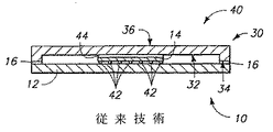
従来技術の半導体パッケージを図1〜4に関連して説明する。初めに、図1を参照すると、パッケージはベース10と蓋30とを備え、これらは初めに個別の部品として供給される。ベース10は基板12を備えることができ、この基板12は、例えば回路基板のような回路保持構造であることができる。半導体チップ14が、回路保持構造12の回路と電気的に接続した状態で提供され、例えば、半田ビードによる電気相互接続(図1では見ることができない)を用いてそのような回路に接続することができる。封止材料16が、回路保持構造12の外周に設けられ、この封止部材16は、例えば、エポキシを含むことができる。図1に示すベース10の表面は、最終的には、蓋30で形成されるパッケージ構造の内側表面となる。
【0004】
蓋30を参照すると、この蓋は、窪んでいない周囲部分34で囲まれた窪んだ表面32を備える。また、蓋30は、表面32に対して反対側の関係にある、したがって、図1の図の蓋30の隠れた下側の面である表面36を備える。蓋30の表面32は、最終的には、蓋30とベース10とで形成されるパッケージの蓋の内側表面になり、表面36はそのようなパッケージの外側表面になる。
【0005】
図2は、蓋30およびベース10を備えるパッケージ40の上面図を示す。パッケージ40を形成するプロセスステップは、図1に示す構成から蓋30をひっくり返し、さらにベース10の上に蓋を押し付けることである。封止材16で蓋30の周囲部分34をベースに対して封止することによって、蓋30をベース10に封止する。
【0006】
図3は、図2のパッケージ40の断面図を示し、ベース10と接合された蓋30を示す。また、図3には、チップ14から下方に延びて、基板12に保持された回路(図示しない)とチップとを電気的に接続する電気相互接続42を見ることができる。さらに、図3は、チップ14に形成され蓋30をチップ14と熱的に接続して、チップ14から蓋30への熱の発散を可能にする、熱伝導を可能にする接続手段すなわち熱伝導性インターフェース材料44を示す。材料44が存在しないか、またはこれが非熱伝導性材料に置き換えられると、蓋30はただ単にマイクロ電子部品用蓋である。しかし、材料44が熱伝導性材料である場合、蓋30は熱スプレッダとして機能する。ここで、熱スプレッダという用語は、3次元ではなくて2次元に主に熱を広げる構造体を示すものと理解される。
【0007】
図4は、熱伝導性インターフェース材料52を介してヒートシンク50に取り付けられた図3のパッケージ40を示す。材料52は、例えば、Honeywell International,Inc.から市販されているGELVET(商標)を含むことができる。ヒートシンク50は、例えば、多数の隆起するフィンおよび/または柱を一体化する形のアルミニウムを含むことができる。ヒートシンク50は、2次元ではなくて3次元に熱を発散する点で、熱スプレッダと区別される。
【0008】
蓋30のような複雑な蓋を作ることは、問題があり、さらに費用がかかる。したがって、改良されたマイクロ電子部品用蓋の設計を開発することが望まれている。
【0009】
(発明の概要)
本発明は、マイクロ電子部品用パッケージの蓋、熱スプレッダ、およびマイクロ電子部品用蓋または熱スプレッダを備える半導体パッケージを含む。本発明の特定の態様では、マイクロ電子部品用蓋は、4つ辺を画定する周縁が四角形である材料を含む。さらに、この蓋は、全周に満たない縁に沿って隆起する周縁レールを有する。例えば、この蓋はその辺のうちの2辺だけに沿って隆起する周縁レールを有することができる。もしくは、そのようなマイクロ電子部品用蓋は、周囲の4つの縁(辺)を画定する一般的な四角形の形態のものを含み、その縁のうちの2つが他の2つの縁よりもより厚いものとして説明することができる。
【0010】
また、上記の形のマイクロ電子部品用蓋を有し、かつ少なくとも100ワット/メートル・ケルビン、好ましくは少なくとも150ワット/メートル・ケルビン、さらに最も好ましくは200ワット/メートル・ケルビン以上の熱伝導率の材料を備える熱スプレッダを、本発明は含む。特定の実施形態では、この熱スプレッダは、銅を含むか、銅から成るか、または基本的に銅から成ることができ、さらに約350ワット/メートル・ケルビンの熱伝導率を有することができる。他の実施形態では、熱スプレッダはアルミニウムを含むか、アルミニウムから成るか、または基本的にアルミニウムから成ることができ、さらに220ワット/メートル・ケルビンの熱伝導率を有することができる。
【0011】
本発明の好ましい実施形態は、次の添付の図面を参照して以下で説明する。
【0012】
(好ましい実施形態の詳細な説明)
本発明に含まれるマイクロ電子部品用蓋あるいはヒートシンクは、図5を参照して説明し、蓋100として全体を示す。蓋100は、全体として四角形の形である(本発明には他の形も含まれ、そのような他の形には、例えば、円形、三角形、五角形、または他の多角形が含まれる)。蓋100は、4つの縁102、104、106および108で画定される周囲を含む。また、蓋100は、縁102および106の表面と同じ平面で広がるくぼんだ表面110および、縁(辺)108および104に沿って延びる隆起レール112および114を含む。さらに、蓋100は、表面110に対して反対側にある表面120(図5の図では見えない)を含む。
【0013】
図5の蓋100と従来技術の蓋30(図1に示す)との違いは、蓋100が蓋の周囲の部分だけに沿って延びる隆起部(112および114)を有する点にある。対照的に、従来技術の蓋30は、周縁全体に沿って延びる隆起部(34)を有する。
【0014】
図示の実施形態では、蓋100は四角形の形であり、隆起周縁部は、周縁のうちの2つの対向する辺(104と108)に沿っている。一方で、残りの2つの辺(102と106)は、その大部分の範囲に沿って延びる隆起部を有しない。実際に、ただ縁102と106に関連づけられる隆起部は、隆起部112および114の終端部だけであり、かかる終端部は縁102および106に接触する隆起部112および114の領域のものである。レール112および114のそのような終端部を、図5で符号115によって特定する。したがって、縁102は、レール112および114の終端115の間に、この縁102に沿って延びる広がり126を有する。そのような広がり126は、表面110に対して隆起していない。同様に、縁106は、終端115の間に延び、表面110に対して隆起していない広がり128を有する。
【0015】
図6は、辺106に沿った蓋100の側面図を示す。そのような側面図は、表面110に対するレール112および114の関係を示し、さらにレール112と114の間に延びる広がり128を示す。レール112および114は、その間に延びる溝119を画定する。
【0016】
図5および6の蓋100の例示的な寸法は、約35±0.35ミリメートルの幅「W」、約35±0.35ミリメートルの長さ「L」、および約4.6±0.05ミリメートルの厚さ「T」である。さらに、溝119は約0.6±0.025ミリメートルの深さ「D」を有することができる。
【0017】
次に図7を参照すると、蓋100をベース150の隣に示すが、最終的には、このベースが蓋100で覆われてパッケージを形成する。ベース150は、4つの縁(151、153、155および157)を含み、基板12の上にダイ14を含むという点で図1のベース10に似ている。さらに、ベース150は、基板の周縁に沿って設けられた封止材16を備える。しかし、図7のベース150とベース10との違いは、封止材16が、ベース10で行われたように4つの周囲の縁に沿ってではなくて、ベース150の基板12の周囲の縁のうちの2つだけに沿って設けられることである。封止材16は、ベース150の基板12の周囲の2つの縁に沿って設けられ、この2つの縁が、最終的には、蓋100に関連した隆起した縁に接触する。
【0018】
図7の処理ステップに続く処理ステップで、蓋100はベース150の上に配置され、レール112および114が封止材16でベースに対して封止されてパッケージを形成する。そのようなパッケージをパッケージ200として図8に示し、特に、蓋100の表面120が見える状態で上面図に示す。
【0019】
次に図9を参照すると、図8の線9−9に沿った断面図でパッケージ200を示す。この断面図は、ダイ14を基板12と接続する半田ビード42を示す。また、この断面図は、ダイ14と蓋100との間に形成された層202を示す。層202は、例えば、熱伝導性材料を、熱伝導を可能にする手段として含むことができる。層202が熱伝導性材料を含む場合、蓋100は一般に、ダイ14で生成される熱を放散するように熱スプレッダとして機能することができる。他の実施形態では、層202は省略することができるか、または非熱伝導性材料に置き換えることができる。そのような他の実施形態のいずれかでは、蓋100は、ダイ14を保護するマイクロ電子部品用蓋として機能するが、一般にダイ14から効果的に熱を放散せず、したがって、熱スプレッダとして使用されない。
【0020】
蓋100が熱スプレッダとして使用される場合、蓋100は、少なくとも100ワット/メートル・ケルビン、より完全に近くは少なくとも150ワット/メートル・ケルビンの熱伝導率を有する材料を含むのが好ましい。特定の実施形態では、蓋100は、例えば、銅またはアルミニウムのような200ワット/メートル・ケルビンを超える熱伝導率を有する材料を含むことができる。蓋100が金属材料を含む実施形態では、蓋100はニッケルメッキすることができる。例えば、蓋100が銅またはアルミニウムを含む場合、少なくとも約3ミクロンの厚さのニッケルメッキを蓋100に施すことができる。ニッケルメッキは、下の蓋材料を腐食から保護することができ、さらに、エポキシへの付着はもちろんのこと、1つまたは複数の熱インターフェース材料への付着のために再現性のある表面を実現することができる。
【0021】
図10を参照すると、パッケージ200の上にヒートシンク50を形成した後のパッケージ200を示し、熱インターフェース52がヒートシンク50をパッケージ200と接続している。ヒートシンク50と熱インターフェース52は、例えば、図4の従来技術構造に関連して上で説明した材料を含むことができる。
【0022】
図11を参照すると、図8のパッケージ200を側面図で示す。チップ(14)は、図面を簡単化するために側面図である図11には示さないが、例えば、図9で示すように、チップ14がパッケージ200の中心にあることを理解すべきである。図11の図は、レール112と114との間の空間に対応してパッケージ200の端部にギャップ250があることを示している。このギャップは一般に狭く、本発明の特定の実施形態では、充填されないままになっていることがある。しかし、ギャップ250を埋めて汚れまたは他の汚染物質が蓋100と基板150の間に侵入するのを防ぐことが望ましい場合、ギャップ内に充填材料を供給することで、そのようなものを実現することができる。この例を図12に示し、ここでは、ギャップ250に充填材料260が充填されている。充填材料260は、例えば、エポキシを含むことができる。パッケージ200の形成後に、充填材料をギャップに塗り込むことで、充填材料260を供給することができる。もしくは、パッケージ200の形成前に、例えば図7の処理ステップで、基板150の縁151および153に充填材料を供給することで、充填材料250を供給することができる。
【0023】
本発明の蓋100は、従来技術の蓋(例えば、図1の蓋30のようなもの)に比べて、蓋100が従来技術の蓋よりも製造するのが簡単であるという点で有利である。蓋100は、例えば、図13および14の処理で形成することができる。最初に図13を参照すると、蓋の原材料の棒300が供給される。この棒は、寸法「A」、「X」、および「Y」を備える。寸法「X」は、完成した蓋100(図5および6)の縁106に沿った幅に対応し、寸法「Y」は、完成した蓋100のレール112および114の厚さに対応する。寸法「A」は、完成した蓋100の縁108の5、6倍の長さよりも長いのが好ましい。
【0024】
次に図14を参照すると、棒300は、棒の表面に沿って延びる溝302を形成するように機械加工される。溝302は、蓋の原材料の辺に沿って延びるレール112および114を画定する。続いて、この原材料を点線304および306に沿って切断して、個別の蓋100、400および500を画定することができる。蓋の材料に金属メッキが望ましい場合、分離された蓋は、続いて電気メッキに供することができる。
【0025】
図13および14は、蓋の原材料棒300を機械加工して溝302を形成するプロセスを示すが、本発明には、蓋材料を図示の形に押し出し成形することにより図14の溝を掘った材料を形成する、他の処理が含まれることを理解すべきである。
【図面の簡単な説明】
【図1】
パッケージを形成する従来技術方法の準備段階でのマイクロ電子部品用パッケージを示す概略図であり、ベースから分離した蓋を含む。蓋は底面図で示し、ベースは上面図で示す。
【図2】
図1の蓋およびベースを備えるパッケージを示す上面図である。
【図3】
線3−3に沿った図2のパッケージを示す図である。
【図4】
図3の処理ステップに続く処理ステップでの、図3の断面図に沿った図2のパッケージを示す図である。
【図5】
本発明が含むマイクロ電子部品用蓋あるいは熱スプレッダを示す概略底面図である。
【図6】
図5の蓋を示す側面図である。
【図7】
本発明が含むマイクロ電子部品用パッケージを形成する準備段階での、ベースと組み合わせた図5の蓋を示す図である。図7のベースは上面図で示すが、蓋は底面図で示す。
【図8】
図7の蓋およびベースを使用して組み立てられたパッケージを示す上面図である。
【図9】
線9−9に沿った図8のパッケージを示す断面図である。
【図10】
図9の処理ステップに続く処理ステップでの、線9−9に沿った図8のパッケージを示す断面図である。
【図11】
図8のパッケージを示す側面図である。
【図12】
図11の実施形態と異なる本発明の実施形態に従った、図8のパッケージを示す側面図である。
【図13】
本発明の方法に従って蓋を形成する準備段階での1個の蓋原材料を示す等角図である。
【図14】
図13の処理ステップに続く処理ステップでの、図13の蓋原材料を示す等角図である。[0001]
(Technical field)
The present invention relates to the design of a lid for a microelectronic component, the design of a heat spreader (heat dissipating member), and the mounting of a semiconductor.
[0002]
(Background of the Invention)
Current semiconductor device packaging generally involves providing a lid for a microelectronic component on a semiconductor die (also called a chip) to protect the die during transport. Since the lid for the microelectronic component is in thermal communication with the die, the heat generated by the die is dissipated to the lid. Thus, this lid can function as a heat spreader in addition to functioning as a protective cover for the die.
[0003]
A prior art semiconductor package will be described with reference to FIGS. Referring initially to FIG. 1, the package comprises a
[0004]
Referring to
[0005]
FIG. 2 shows a top view of the
[0006]
FIG. 3 shows a cross-sectional view of the
[0007]
FIG. 4 shows the
[0008]
Making complex lids, such as
[0009]
(Summary of the Invention)
The present invention includes a microelectronic component package lid, a heat spreader, and a semiconductor package including the microelectronic component lid or heat spreader. In a particular aspect of the invention, the lid for a microelectronic component comprises a quadrilateral material defining four sides. In addition, the lid has a peripheral rail that rises along less than a full edge. For example, the lid may have a peripheral rail that rises along only two of its sides. Alternatively, such microelectronic component lids include those in the form of a general rectangle defining four surrounding edges, two of which are thicker than the other two edges. Can be described as
[0010]
It also has a lid for a microelectronic component of the above type and has a thermal conductivity of at least 100 Watts / meter-Kelvin, preferably at least 150 Watts / meter-Kelvin, and most preferably at least 200 Watts / meter-Kelvin The present invention includes a heat spreader comprising a material. In certain embodiments, the heat spreader can include, consist of, or consist essentially of copper, and can have a thermal conductivity of about 350 watts / meter Kelvin. In other embodiments, the heat spreader can include, consist of, or consist essentially of aluminum and can have a thermal conductivity of 220 watts / meter Kelvin.
[0011]
Preferred embodiments of the present invention are described below with reference to the following accompanying drawings.
[0012]
(Detailed description of preferred embodiments)
The lid or heat sink for a microelectronic component included in the present invention will be described with reference to FIG. Lid 100 is generally square shaped (the invention includes other shapes, such as, for example, circular, triangular, pentagonal, or other polygonal shapes). Lid 100 includes a perimeter defined by four edges 102, 104, 106 and 108. Lid 100 also includes a concave surface 110 that extends coplanar with the surfaces of edges 102 and 106 and raised rails 112 and 114 that extend along edges 108 and 104. In addition, the lid 100 includes a surface 120 (not visible in FIG. 5) that is opposite the surface 110.
[0013]
The difference between the lid 100 of FIG. 5 and the prior art lid 30 (shown in FIG. 1) is that the lid 100 has ridges (112 and 114) that extend only along the perimeter of the lid. In contrast, the
[0014]
In the illustrated embodiment, the lid 100 is rectangular in shape, with the raised perimeter along two opposite sides (104 and 108) of the perimeter. On the other hand, the remaining two sides (102 and 106) have no ridges extending along most of their extent. In fact, the only ridges associated with edges 102 and 106 are the ends of ridges 112 and 114, which are in the region of ridges 112 and 114 that contact edges 102 and 106. Such terminations of rails 112 and 114 are identified by reference numeral 115 in FIG. Thus, the rim 102 has an extension 126 extending along the rim 102 between the terminal ends 115 of the rails 112 and 114. Such an extension 126 is not raised relative to surface 110. Similarly, the rim 106 extends between the termini 115 and has a non-raised extent 128 relative to the surface 110.
[0015]
FIG. 6 shows a side view of lid 100 along side 106. Such a side view illustrates the relationship of the rails 112 and 114 to the surface 110 and further illustrates the extent 128 extending between the rails 112 and 114. Rails 112 and 114 define a groove 119 extending therebetween.
[0016]
Exemplary dimensions of the lid 100 of FIGS. 5 and 6 include a width “W” of about 35 ± 0.35 millimeters, a length “L” of about 35 ± 0.35 millimeters, and about 4.6 ± 0.05. Millimeter thickness "T". Further, groove 119 can have a depth "D" of about 0.6 ± 0.025 millimeters.
[0017]
Referring now to FIG. 7, the lid 100 is shown next to the base 150, which will eventually be covered with the lid 100 to form a package. Base 150 is similar to
[0018]
In a processing step following the processing step of FIG. 7, the lid 100 is placed on the base 150 and the rails 112 and 114 are sealed to the base with the
[0019]
Referring now to FIG. 9, package 200 is shown in a cross-sectional view along line 9-9 in FIG. This cross-sectional view shows a
[0020]
If the lid 100 is used as a heat spreader, the lid 100 preferably comprises a material having a thermal conductivity of at least 100 Watts / meter-Kelvin, more fully at least 150 Watts / meter-Kelvin. In certain embodiments, lid 100 can include a material having a thermal conductivity greater than 200 Watts / meter-Kelvin, such as, for example, copper or aluminum. In embodiments where the lid 100 includes a metal material, the lid 100 may be nickel plated. For example, if the lid 100 includes copper or aluminum, the lid 100 may be plated with nickel at least about 3 microns thick. Nickel plating can protect the underlying lid material from corrosion, and also provides a reproducible surface for adhesion to one or more thermal interface materials as well as to epoxy be able to.
[0021]
Referring to FIG. 10, the package 200 is shown after the
[0022]
Referring to FIG. 11, the package 200 of FIG. 8 is shown in a side view. Chip (14) is not shown in FIG. 11, which is a side view for simplicity, but it should be understood that
[0023]
The lid 100 of the present invention is advantageous in that the lid 100 is easier to manufacture than prior art lids, as compared to prior art lids (such as
[0024]
Referring now to FIG. 14, the bar 300 is machined to form a groove 302 that extends along the surface of the bar. Grooves 302 define rails 112 and 114 that extend along the sides of the lid material. Subsequently, the raw material can be cut along dotted lines 304 and 306 to define individual lids 100, 400 and 500. If metal plating is desired for the lid material, the separated lid can then be subjected to electroplating.
[0025]
FIGS. 13 and 14 show the process of machining the lid raw material bar 300 to form the groove 302, but the present invention digs the groove of FIG. 14 by extruding the lid material into the shape shown. It should be understood that other processes for forming the material are included.
[Brief description of the drawings]
FIG.
1 is a schematic diagram illustrating a package for microelectronic components in a preparatory stage of a prior art method of forming a package, including a lid separated from a base. The lid is shown in a bottom view and the base is shown in a top view.
FIG. 2
FIG. 2 is a top view showing a package including the lid and the base of FIG. 1.
FIG. 3
FIG. 3 shows the package of FIG. 2 along line 3-3.
FIG. 4
FIG. 4 shows the package of FIG. 2 along the cross-sectional view of FIG. 3 at a processing step following the processing step of FIG. 3.
FIG. 5
FIG. 3 is a schematic bottom view showing a lid or a heat spreader for a micro electronic component included in the present invention.
FIG. 6
It is a side view which shows the lid of FIG.
FIG. 7
FIG. 6 is a view showing the lid of FIG. 5 combined with a base in a preparation stage of forming a package for a microelectronic component included in the present invention. The base in FIG. 7 is shown in a top view, while the lid is shown in a bottom view.
FIG. 8
FIG. 8 is a top view showing a package assembled using the lid and the base of FIG. 7.
FIG. 9
FIG. 9 is a cross-sectional view showing the package of FIG. 8 along line 9-9.
FIG. 10
FIG. 10 is a cross-sectional view of the package of FIG. 8 taken along line 9-9 at a processing step following the processing step of FIG. 9;
FIG. 11
FIG. 9 is a side view showing the package of FIG. 8.
FIG.
FIG. 12 is a side view showing the package of FIG. 8 according to an embodiment of the present invention that is different from the embodiment of FIG. 11.
FIG. 13
1 is an isometric view showing one lid raw material in preparation for forming a lid according to the method of the present invention.
FIG. 14
14 is an isometric view of the lid raw material of FIG. 13 in a processing step following the processing step of FIG.
Claims (36)
形および前記形を囲繞する周縁を有する蓋材料と、
前記周縁で囲繞された表面と、
前記周縁の一部分だけに沿って延び、かつ前記表面に対して高く隆起したレールとを備えるマイクロ電子部品用蓋。A lid for a microelectronic component,
A lid material having a shape and a perimeter surrounding said shape;
A surface surrounded by the periphery,
A rail extending along only a portion of the perimeter and having a raised rail relative to the surface.
ベースと、
前記ベースによって支持されたチップと、
前記チップを覆う前記マイクロ電子部品用蓋とを備え、それによって、前記チップが前記マイクロ電子部品用蓋と前記ベースとの間に実装される請求項1に記載のマイクロ電子部品用蓋。The lid for a microelectronic component according to claim 1, which is incorporated in a package for a microelectronic component, wherein the package comprises:
Base and
A chip supported by the base,
The lid for a microelectronic component according to claim 1, further comprising the lid for the microelectronic component covering the chip, wherein the chip is mounted between the lid for the microelectronic component and the base.
蓋用原材料の棒を供給するステップと、
前記棒の側面に沿って溝を形成するステップと、
前記溝を形成した後で、前記棒を複数の個別のマイクロ電子部品用蓋に切断するステップとを含む方法。A method of forming a plurality of microelectronic component lids,
Providing a rod of lid material;
Forming a groove along the side of the rod;
Cutting the rod into a plurality of individual microelectronic component lids after forming the groove.
ベースで支持されたチップを供給するステップと、
前記マイクロ電子部品用蓋を、前記チップを覆うようにして前記ベースに付着するステップとを含み、それによって、前記チップを前記マイクロ電子部品用蓋と前記ベースとの間に実装するようにした、請求項25に記載の方法。Further comprising incorporating at least one of the microelectronic component lids into a microelectronic component package;
Providing a chip supported by the base;
Attaching the lid for the microelectronic component to the base so as to cover the chip, whereby the chip is mounted between the lid for the microelectronic component and the base. A method according to claim 25.
蓋原材料を、側面と前記側面に沿って延びる溝とを有する棒の形に押し出し成形するステップと、
前記材料を押し出し成形した後で、前記棒を複数の個別のマイクロ電子部品用蓋に切断するステップとを含む方法。A method of forming a plurality of microelectronic component lids,
Extruding the lid raw material into a rod having a side surface and a groove extending along the side surface;
After extruding the material, cutting the bar into a plurality of individual microelectronic component lids.
ベースで支持されたチップを供給するステップと、
前記マイクロ電子部品用蓋を、前記チップを覆うようにして前記ベースに付着するステップとを含み、それによって、前記チップが前記マイクロ電子部品用蓋と前記ベースとの間に実装されるようにした、請求項31に記載の方法。Further comprising incorporating at least one of the microelectronic component lids into a microelectronic component package;
Providing a chip supported by the base;
Attaching the lid for the microelectronic component to the base so as to cover the chip, whereby the chip is mounted between the lid for the microelectronic component and the base. 32. The method of claim 31.
Applications Claiming Priority (2)
| Application Number | Priority Date | Filing Date | Title |
|---|---|---|---|
| US24904300P | 2000-11-14 | 2000-11-14 | |
| PCT/US2001/044849 WO2002041394A2 (en) | 2000-11-14 | 2001-10-30 | Lid and heat spreader design for a semiconductor package |
Publications (2)
| Publication Number | Publication Date |
|---|---|
| JP2004528702A true JP2004528702A (en) | 2004-09-16 |
| JP2004528702A5 JP2004528702A5 (en) | 2005-05-19 |
Family
ID=22941809
Family Applications (1)
| Application Number | Title | Priority Date | Filing Date |
|---|---|---|---|
| JP2002543696A Withdrawn JP2004528702A (en) | 2000-11-14 | 2001-10-30 | Microelectronic component lids, thermal spreaders, and semiconductor packages |
Country Status (7)
| Country | Link |
|---|---|
| US (2) | US6958536B2 (en) |
| EP (1) | EP1336199A2 (en) |
| JP (1) | JP2004528702A (en) |
| KR (1) | KR20040014412A (en) |
| CN (1) | CN1575520A (en) |
| AU (1) | AU2002217965A1 (en) |
| WO (1) | WO2002041394A2 (en) |
Families Citing this family (9)
| Publication number | Priority date | Publication date | Assignee | Title |
|---|---|---|---|---|
| US6888238B1 (en) * | 2003-07-09 | 2005-05-03 | Altera Corporation | Low warpage flip chip package solution-channel heat spreader |
| DE112004002702B4 (en) * | 2004-02-03 | 2009-03-05 | Infineon Technologies Ag | Method for producing a semiconductor assembly and matrix assembly |
| KR100799614B1 (en) | 2006-05-23 | 2008-01-30 | 삼성전기주식회사 | Mems module package having heat spreading function |
| JP2011514663A (en) * | 2008-01-31 | 2011-05-06 | レイセオン カンパニー | Method and apparatus for heat transfer of parts |
| WO2012074775A1 (en) * | 2010-11-19 | 2012-06-07 | Analog Devices, Inc. | Packaged integrated device with electrically conductive lid |
| CN104192790A (en) * | 2014-09-15 | 2014-12-10 | 华东光电集成器件研究所 | Thermal stress isolation structure for MEMS (micro-electromechanical system) device |
| US9837333B1 (en) | 2016-09-21 | 2017-12-05 | International Business Machines Corporation | Electronic package cover having underside rib |
| US10622282B2 (en) * | 2017-07-28 | 2020-04-14 | Qualcomm Incorporated | Systems and methods for cooling an electronic device |
| US20230320039A1 (en) * | 2022-04-05 | 2023-10-05 | Honeywell International Inc. | Integrated heat spreader |
Family Cites Families (14)
| Publication number | Priority date | Publication date | Assignee | Title |
|---|---|---|---|---|
| KR860002865A (en) * | 1984-09-04 | 1986-04-30 | 로버어트 티이 오어너 | Integrated circuit package with integrated heat dissipation device |
| US5831836A (en) * | 1992-01-30 | 1998-11-03 | Lsi Logic | Power plane for semiconductor device |
| US5459352A (en) * | 1993-03-31 | 1995-10-17 | Unisys Corporation | Integrated circuit package having a liquid metal-aluminum/copper joint |
| US5485037A (en) | 1993-04-12 | 1996-01-16 | Amkor Electronics, Inc. | Semiconductor device having a thermal dissipator and electromagnetic shielding |
| US5956576A (en) * | 1996-09-13 | 1999-09-21 | International Business Machines Corporation | Enhanced protection of semiconductors with dual surface seal |
| US6075289A (en) | 1996-10-24 | 2000-06-13 | Tessera, Inc. | Thermally enhanced packaged semiconductor assemblies |
| TW359863B (en) | 1997-11-28 | 1999-06-01 | Utron Technology Inc | Multi-chip stack package |
| JP3097644B2 (en) | 1998-01-06 | 2000-10-10 | 日本電気株式会社 | Semiconductor device connection structure and connection method |
| US6068051A (en) * | 1998-03-23 | 2000-05-30 | Intel Corporation | Channeled heat sink |
| JP2000022044A (en) | 1998-07-02 | 2000-01-21 | Mitsubishi Electric Corp | Semiconductor device and its manufacture |
| US6118177A (en) * | 1998-11-17 | 2000-09-12 | Lucent Technologies, Inc. | Heatspreader for a flip chip device, and method for connecting the heatspreader |
| US6091603A (en) | 1999-09-30 | 2000-07-18 | International Business Machines Corporation | Customizable lid for improved thermal performance of modules using flip chips |
| US6222263B1 (en) | 1999-10-19 | 2001-04-24 | International Business Machines Corporation | Chip assembly with load-bearing lid in thermal contact with the chip |
| US6784540B2 (en) * | 2001-10-10 | 2004-08-31 | International Rectifier Corp. | Semiconductor device package with improved cooling |
-
2001
- 2001-10-30 WO PCT/US2001/044849 patent/WO2002041394A2/en not_active Application Discontinuation
- 2001-10-30 AU AU2002217965A patent/AU2002217965A1/en not_active Abandoned
- 2001-10-30 JP JP2002543696A patent/JP2004528702A/en not_active Withdrawn
- 2001-10-30 CN CNA018219918A patent/CN1575520A/en active Pending
- 2001-10-30 KR KR10-2003-7006558A patent/KR20040014412A/en not_active Application Discontinuation
- 2001-10-30 EP EP01996884A patent/EP1336199A2/en not_active Withdrawn
- 2001-10-30 US US10/416,824 patent/US6958536B2/en not_active Expired - Fee Related
-
2004
- 2004-04-12 US US10/823,117 patent/US20040187309A1/en not_active Abandoned
Also Published As
| Publication number | Publication date |
|---|---|
| AU2002217965A1 (en) | 2002-05-27 |
| US20040187309A1 (en) | 2004-09-30 |
| US6958536B2 (en) | 2005-10-25 |
| US20040070069A1 (en) | 2004-04-15 |
| EP1336199A2 (en) | 2003-08-20 |
| CN1575520A (en) | 2005-02-02 |
| KR20040014412A (en) | 2004-02-14 |
| WO2002041394A3 (en) | 2003-05-15 |
| WO2002041394A2 (en) | 2002-05-23 |
Similar Documents
| Publication | Publication Date | Title |
|---|---|---|
| US6330158B1 (en) | Semiconductor package having heat sinks and method of fabrication | |
| US6737750B1 (en) | Structures for improving heat dissipation in stacked semiconductor packages | |
| US6921683B2 (en) | Semiconductor device and manufacturing method for the same, circuit board, and electronic device | |
| JP4195380B2 (en) | Semiconductor device package with improved cooling | |
| US5650662A (en) | Direct bonded heat spreader | |
| US5429992A (en) | Lead frame structure for IC devices with strengthened encapsulation adhesion | |
| US7061080B2 (en) | Power module package having improved heat dissipating capability | |
| KR101740496B1 (en) | Semiconductor die package including low stress configuration | |
| JPH05206338A (en) | Assembly of semiconductor device provided with heat sink | |
| CN104051376A (en) | Power overlay structure and method of making same | |
| JP2005506691A5 (en) | ||
| JP2010021515A (en) | Semiconductor device and its manufacturing method | |
| KR19980058198A (en) | Bottom Lead Semiconductor Package | |
| US7399657B2 (en) | Ball grid array packages with thermally conductive containers | |
| CN110416097A (en) | The encapsulating structure and packaging method for preventing indium metal from overflowing | |
| JP2004528702A (en) | Microelectronic component lids, thermal spreaders, and semiconductor packages | |
| US6847102B2 (en) | Low profile semiconductor device having improved heat dissipation | |
| JP3336982B2 (en) | Semiconductor device and method of manufacturing the same | |
| US7768104B2 (en) | Apparatus and method for series connection of two die or chips in single electronics package | |
| JP2001118953A (en) | Manufacturing method of semiconductor electronic part | |
| JP2002329804A (en) | Semiconductor device | |
| JPH0473297B2 (en) | ||
| JP3313009B2 (en) | Heat dissipation member, lead frame and semiconductor device | |
| JPS6220701B2 (en) | ||
| TW586169B (en) | Semiconductor die package with semiconductor die having side electrical connection |
Legal Events
| Date | Code | Title | Description |
|---|---|---|---|
| A621 | Written request for application examination |
Free format text: JAPANESE INTERMEDIATE CODE: A621 Effective date: 20041101 |
|
| A072 | Dismissal of procedure [no reply to invitation to correct request for examination] |
Free format text: JAPANESE INTERMEDIATE CODE: A073 Effective date: 20050527 |
|
| A300 | Application deemed to be withdrawn because no request for examination was validly filed |
Free format text: JAPANESE INTERMEDIATE CODE: A300 Effective date: 20050607 |