JP2004509487A - In-band on-channel broadcasting system for digital data - Google Patents
In-band on-channel broadcasting system for digital data Download PDFInfo
- Publication number
- JP2004509487A JP2004509487A JP2002514930A JP2002514930A JP2004509487A JP 2004509487 A JP2004509487 A JP 2004509487A JP 2002514930 A JP2002514930 A JP 2002514930A JP 2002514930 A JP2002514930 A JP 2002514930A JP 2004509487 A JP2004509487 A JP 2004509487A
- Authority
- JP
- Japan
- Prior art keywords
- signal
- carrier
- pulse
- stereo
- broadcast
- Prior art date
- Legal status (The legal status is an assumption and is not a legal conclusion. Google has not performed a legal analysis and makes no representation as to the accuracy of the status listed.)
- Granted
Links
Images


Classifications
-
- H—ELECTRICITY
- H04—ELECTRIC COMMUNICATION TECHNIQUE
- H04H—BROADCAST COMMUNICATION
- H04H20/00—Arrangements for broadcast or for distribution combined with broadcast
- H04H20/28—Arrangements for simultaneous broadcast of plural pieces of information
- H04H20/30—Arrangements for simultaneous broadcast of plural pieces of information by a single channel
-
- H—ELECTRICITY
- H04—ELECTRIC COMMUNICATION TECHNIQUE
- H04H—BROADCAST COMMUNICATION
- H04H20/00—Arrangements for broadcast or for distribution combined with broadcast
- H04H20/44—Arrangements characterised by circuits or components specially adapted for broadcast
- H04H20/46—Arrangements characterised by circuits or components specially adapted for broadcast specially adapted for broadcast systems covered by groups H04H20/53-H04H20/95
- H04H20/47—Arrangements characterised by circuits or components specially adapted for broadcast specially adapted for broadcast systems covered by groups H04H20/53-H04H20/95 specially adapted for stereophonic broadcast systems
-
- H—ELECTRICITY
- H04—ELECTRIC COMMUNICATION TECHNIQUE
- H04H—BROADCAST COMMUNICATION
- H04H2201/00—Aspects of broadcast communication
- H04H2201/10—Aspects of broadcast communication characterised by the type of broadcast system
- H04H2201/18—Aspects of broadcast communication characterised by the type of broadcast system in band on channel [IBOC]
- H04H2201/183—FM digital or hybrid
Abstract
FM放送送信機(図5)は、搬送波を中心とする伝送帯域幅内でフル・パワーで伝送可能であり、放送周波数の搬送波および側波帯を有する放送信号を伝送する。これには、放送周波数での搬送波を有し、ステレオ信号を表す、伝送帯域幅よりも狭い帯域幅を備えた側波帯を有する変調FMステレオ信号の発生源(source)が含まれる。さらに、可変パルス幅符号化信号として符号化されたIBOCデジタル・データ信号を表す、互いを基準として間隔を空けて配置された搬送波パルスと、FMステレオ信号側波帯と重複することのない、伝送帯域幅内の帯域幅を有する変調IBOC信号の発生源(source)も含まれる。信号コンバイナは、変調FMステレオ信号と変調IBOC信号を組み合わせて放送信号を形成する。FM放送受信機(図6)は、FMステレオ信号を表す第1の変調信号と、可変パルス幅符号化信号として符号化されたイン・バンド・オン・チャネル(IBOC)デジタル・データ信号を表す、互いを基準として間隔を空けて配置された搬送波パルスを有する第2の変調信号とを含む放送信号を受け取る。これは、FMステレオ信号を表す第1の分離された信号と、IBOCデジタル・データ信号を表す第2の分離された信号とを生成する信号セパレータを含む。FM信号処理装置は、FMステレオ信号によって表されるステレオ・オーディオ信号を生成する。IBOC信号処理装置は、IBOCデジタル・データ信号によって表されるデジタル・データ信号を生成する。The FM broadcast transmitter (FIG. 5) can transmit at full power within a transmission bandwidth centered on a carrier wave, and transmits a broadcast signal having a carrier wave and a sideband of a broadcast frequency. This includes a source of a modulated FM stereo signal having a sideband with a narrower bandwidth than the transmission bandwidth, having a carrier at the broadcast frequency and representing a stereo signal. Further, a carrier pulse, spaced apart from one another, representing an IBOC digital data signal encoded as a variable pulse width encoded signal, and transmission without overlapping the FM stereo signal sidebands. A source of a modulated IBOC signal having a bandwidth within the bandwidth is also included. The signal combiner combines the modulated FM stereo signal and the modulated IBOC signal to form a broadcast signal. The FM broadcast receiver (FIG. 6) represents a first modulated signal representing an FM stereo signal and an in-band-on-channel (IBOC) digital data signal encoded as a variable pulse width encoded signal. A second modulated signal having carrier pulses spaced apart from each other. It includes a signal separator that produces a first separated signal representing the FM stereo signal and a second separated signal representing the IBOC digital data signal. The FM signal processing device generates a stereo audio signal represented by the FM stereo signal. The IBOC signal processor generates a digital data signal represented by the IBOC digital data signal.
Description
【0001】
本発明は、帯域制限チャネル(band limited channels)を介して高速データ・レートを提供する変調技法に関し、具体的に言えば、デジタル・データ、特にデジタル・オーディオのためのイン・バンド・オン・チャネル(IBOC)FM放送変調システムに関する。
【0002】
米国では、FM放送会社は、自らに割り当てられた搬送波周波数から100kHz以内の側波帯においてはフル・パワーで、搬送波を中心として100kHzから200kHzの周波数範囲内にある側波帯においてはフル・パワーから30dB低下した出力で、情報を伝送することができる。標準のステレオ・オーディオ信号は、搬送波から53kHz以内の帯域幅に配置される。したがって放送会社は、上記の制約を受けながら、残りの帯域幅で他の情報を伝送することができる。
【0003】
FM放送会社にとっては、ステレオ・オーディオ・データとデジタル・データとを同時に放送することが望ましくなってきている。たとえば、そのデジタル・データは、放送されるステレオ・オーディオの高品質バージョンを表すことができる。そのためには、比較的高速のデータ・レート・チャネルが必要であるが、そのチャネルは、比較的狭い帯域幅に制限される。たとえば、高品質オーディオを搬送するデジタル・データ・ストリームは、毎秒128キロビット(KBPS)のビット・レートを有する場合がある。こうしたデータ・ストリームを搬送する信号は、その信号に必要な帯域幅を減らすための何らかの圧縮形式を使用することなく、FM放送信号で使用可能な帯域幅で伝送することはできない。
【0004】
帯域幅が制限されたチャネルを介して、高速のデータ・レートでデータを提供することが常に望ましい。チャネルを介したデータ・レートを上げるために、これまでにも多くの変調技法が開発されてきた。たとえば、M−ary位相シフト・キード(phase shift keyed)(PSK)および直交振幅変調(QAM)技法は、伝送されるそれぞれのシンボル(symbol)で複数のデータ・ビットを符号化することによって圧縮を可能にする。こうしたシステムには、それらに関連付けられた制約がある。第1に、こうしたシステムに関連付けられたハードウェアは高価である。これは、これらの技法が適切に動作するには、高水準のチャネル線形性(channel linearity)を必要とするためである。したがって、搬送波トラッキング、シンボル・リカバリ(symbol recovery)、補間、および信号成形のために、大規模な信号処理を実行しなければならない。第2に、こうした技法はマルチパス効果に敏感である。これらの効果は、受信機内では補償される必要がある。第3に、これらのシステムは、所望のデータ・レートを得るために、一部のアプリケーション(たとえばイン・バンド・オン・チャネル放送FM副搬送波サービス)で使用可能なものを超えた帯域幅を必要とすることが多い。
【0005】
本発明の原理によれば、FM放送送信機は、放送周波数の搬送波および側波帯を有する放送信号を伝送し、搬送波の周囲の伝送帯域幅以内で、フル・パワーで伝送可能である。これには、放送周波数の搬送波を有し、ステレオ信号を表す伝送帯域幅よりも狭い帯域幅を備えた側波帯を有する、変調されたFMステレオ信号の発生源(source)が含まれる。さらに、可変パルス幅符号化信号として符号化されたIBOCデジタル・データ信号を表す、互いを基準として間隔を空けて配置された搬送波パルスと、FMステレオ信号側波帯と重複することのない、伝送帯域幅内の帯域幅とを有する、変調されたIBOC信号の発生源(source)も含まれる。信号コンバイナは、変調FMステレオ信号と変調IBOC信号を組み合わせて放送信号を形成する。
【0006】
本発明の他の態様によれば、FM放送受信機は、FMステレオ信号を表す第1の変調信号と、可変パルス幅符号化信号として符号化されたイン・バンド・オン・チャネル(IBOC)デジタル・データ信号を表す、互いを基準として間隔を空けて配置された搬送波パルスを有する第2の変調信号とを含む、放送信号を受け取る。このFM放送受信機は、FMステレオ信号を表す第1の分離信号と、IBOCデジタル・データ信号を表す第2の分離信号とを生成するための、信号セパレータを含む。FM信号処理装置は、FMステレオ信号によって表されるステレオ・オーディオ信号を生成する。IBOC信号処理装置は、IBOCデジタル・データ信号によって表されるデジタル・データ信号を生成する。
【0007】
本発明の原理に従った技法は、比較的高速なデータ・レートのデジタル信号を搬送する第2のチャネルを含む、FM伝送システムを提供する。このチャネルは、フル・パワーで伝送可能なFM帯域幅の一部分に配置される。こうしたチャネルを実施するのに必要な回路は、比較的単純かつ安価である。さらに、高いチャネル線形性を必要とせず、マルチパス問題の対象となることもない。受信機内でこのチャネルを実施するに必要とする追加の回路は比較的小型であり、受信機内に先在するIF回路の出力に結合することができる。
【0008】
図1は、本発明で使用できる変調器のブロック・ダイヤグラムである。図1では、入力端子INがデジタル信号を受け取る。入力端子INは、エンコーダ10の入力端子に結合される。エンコーダ10の出力端子は、微分器(differentiator)20の入力端子に結合される。微分器20の出力端子は、レベル検出器25の入力端子に結合される。レベル検出器25の出力端子は、ミキサ30の第1の入力端子に結合される。ローカル発振器40は、ミキサ30の第2の入力端子に結合される。ミキサ30の出力端子はバンド・パス・フィルタ(BPF)50の入力端子に結合される。BPF50の出力端子は出力端子OUTに結合され、これが入力端子INでのデジタル信号を表す変調された信号を生成する。
【0009】
図2は、図1に示された変調器のオペレーションを理解するのに役立つ波形図である。図2は、波形をより明確に図示するようにスケーリングするために描かれたものではない。例示された実施形態では、入力端子INでのデジタル信号は、非ゼロ復帰(NRZ)フォーマットの2層信号である。この信号は、図2で一番上の波形として示されている。NRZ信号は連続するビットを搬送し、このビットのそれぞれが、NRZ信号で破線によって示されたビット周期と呼ばれる所定の周期の間持続し、ビット・レートと呼ばれる対応する周波数を有する。すべての知られた方法では、NRZ信号のレベルはそのビットの値を表す。エンコーダ10は、可変パルス幅コードを使用してNRZ信号を符号化するように動作する。例示された実施形態では、可変パルス幅コードは可変アパーチャ・コードである。可変アパーチャ・コーディングについては、(発明者)によって(出願日)に出願された米国特許出願(RCA88,945)に詳細に記載されている。この特許出願では、NRZ信号は以下の方法で位相符号化される。
【0010】
NRZ信号の各ビット周期(period)は、符号化信号の遷移(transition)としてコード化される。ビット・レートの倍数Mでの符号化クロックが、NRZ信号を位相符号化するために使用される。上述の特許出願では、符号化クロックはビット・レートの9倍であるレートMで動作する。NRZ信号が論理「1」レベルから論理「0」レベルへ遷移する場合、遷移は前の遷移から符号化信号8符号化クロック・サイクル(M−1)で実行される。NRZ信号が論理「0」レベルから論理「1」レベルへ遷移する場合、遷移は前の遷移から符号化信号10符号化クロック・サイクル(M+1)で実行される。NRZ信号が遷移しない場合、すなわち連続するビットが同じ値を有する場合、遷移は最後の遷移から符号化クロック・サイクル(M)で実行される。可変アパーチャ・コード化信号(VAC)は、図2で第2番目の波形として示されている。
【0011】
可変アパーチャ・コード化信号(VAC)は、微分器20によって微分され、VAC信号の遷移と位置合わせされた一連のパルス時間(series of pulses time)を生成する。微分器はVAC変調信号に対して90度の位相シフトも与える。すべての知られた方法で、前縁遷移(leading edge transition)は正方向パルス(positive−going pulses)を生成し、後縁遷移(trailing edge transition)は負方向パルス(negative−going pulses)を生成する。微分されたVAC信号
【0012】
【数1】
![]()
は、図2で第3番目の信号として示されている。
【0014】
【数2】
![]()
は、一定の振幅を有する一連の3レベル・パルス(series of trilevel pulses)を生成するために、レベル検出器25によって、レベル検出される。すべての知られた方法で、微分されたVAC信号
【0016】
【数3】
![]()
が正のしきい値よりも大きな値を有する場合、レベル信号は高い値(high value)を有して生成され、負のしきい値よりも小さな値を有する場合、レベル信号は低い値(low value)を有して生成され、そうでなければ中心値(center value)を有する。レベル信号は、図2で第4番目の信号(LEVEL)として示されている。
【0018】
LEVEL信号は、ミキサ30でローカル発振器40からの搬送波信号を変調する。正のパルスは第1の位相を有する搬送波信号のパルスを生成し、負のパルスは第2の位相を有する搬送波信号のパルスを生成する。第1および第2の位相は、好ましくはほぼ180度位相がずれている。この搬送波信号パルスは、好ましくはほぼ1つのコーディング・クロック周期長さであり、例示された実施形態では、NRZビット周期のほぼ1/9の持続時間(duration)を有する。ローカル発振器40信号の周波数は、好ましくは搬送波信号パルス時間周期中に少なくとも10サイクルのローカル発振器信号が発生できるように選択される。図2では、搬送波信号CARRは一番下の波形として示されており、搬送波信号はそれぞれの矩形包絡線内の縦のハッチングで表されている。図2に示されたCARR信号では、正方向のLEVELパルスに応答して生成された搬送波パルスの位相は「+」で表され、負方向のLEVELパルスに応答して生成された搬送波パルスの位相は「−」で表されている。「+」および「−」はほぼ180度の位相差のみを表すものであり、任意の絶対位相を表すことを意図するものではない。
【0019】
BPF50は、CARR信号内のすべての「帯域外(out−of−band)」フーリエ構成要素、ならびに搬送波構成要素それ自体および側波帯のうち1つをフィルタリングして取り除き、単一の側波帯信号のみを残す。BPF50からの出力信号OUTは、単側波帯(SSB)位相または入力端子INでのNRZデータ信号を表す周波数変調済み信号である。この信号は、多くの知られた伝送技法のうちいずれかによって受信機に伝送することができる。
【0020】
図3は、図1に示されたように変調された信号を受け取ることができる受信機のブロック・ダイヤグラムである。図3では、入力端子INが、図1および2を参照しながら上記で述べたように変調された信号の発生源(source)に結合される。入力端子INは、BPF110の入力端子に結合される。BPF110の出力端子は、積分器120の入力端子に結合される。積分器120の出力端子は、制限増幅器130の入力端子に結合される。制限増幅器130の出力端子は、検出器140の入力端子に結合される。検出器140の出力端子は、デコーダ150の入力端子に結合される。デコーダ150の出力端子は、入力端子INで変調済み信号によって表されるNRZ信号を再生し、出力端子OUTに結合される。
【0021】
オペレーション時には、BPF 110が帯域外信号をフィルタリングして取り除き、変調済みSSB信号のみを通過させる。積分器120は、微分器20(図1)によってもたらされた90度位相シフトをリバース(reverse)させる。制限増幅器130は、積分器120からの信号の振幅を一定の振幅に制限する。制限増幅器130からの信号は、図2に示された搬送波パルス信号CARRに対応する。検出器140は、FM弁別器または位相ロック・ループ(PLL)のいずれかであり、それぞれFMまたはPM変調された搬送波パルス信号を復調するのに使用される。検出器140は、搬送波パルスを検出し、位相およびそれら位相のタイミングによって表される遷移を有する2レベル信号を生成する。検出器140の出力は、図2のVAC信号に対応する可変ビット幅信号である。デコーダ150はエンコーダ10(図1)の逆のオペレーションを実行し、出力端子OUTで、図2のNRZ信号に対応するNRZ信号を生成する。前述の米国特許出願(RCA第88945号)は、図3で使用することのできるデコーダ150について記載している。出力端子OUTのNRZ信号は、その後、使用回路(utilization circuitry)(図示せず)によって処理される。
【0022】
搬送波パルス(図2の信号CARR)は相互に明確な時間に発生し、それらパルスの持続時間が制限されていることから、パルスが予測される時点にのみ検出器140を実行可能(enable)にすることができる。たとえば例示された実施形態では、上記で詳細に述べたように、各パルスの持続時間はNRZ信号遷移間の時間の、ほぼ1/9である。先行する搬送波パルス(後縁(trailing edge)を表す)以降、NRZ信号遷移間の時間の8/9で搬送波パルスが受け取られた後、そのパルスからのNRZ信号遷移間の時間の9/9(遷移なし)または10/9(前縁)でのみ、後続のパルスが予測される。同様に、先行する搬送波パルス(前縁(leading edge)を表す)以降、NRZ信号遷移間の時間の10/9で搬送波パルスが受け取られた後、そのパルスからのNRZ信号遷移間の時間の8/9(後縁)または9/9(遷移なし)でのみ、後続のパルスが予測される。検出器140は、搬送波パルスが予測されるとき、および予測されるパルスの持続期間の時間的近傍でのみ、実行可能(enable)になればよい。
【0023】
図3に破線160で示されたウィンドウィング・タイマは、検出器140の状況(status)出力端子に結合された入力端子と、検出器140のイネーブル入力端子に結合された出力端子とを有する。ウィンドウィング・タイマ160は検出器140からの信号を監視し、前述のように搬送波パルスが予測される場合のみ、およびそのパルスの持続時間の時間的近傍でのみ、検出器を実行可能(enable)にする。
【0024】
例示された実施形態では、変調済み信号内のエネルギーは、主としてビット・レートの0.44(8/18)倍と0.55(10/18)倍との間にあり、したがってビット・レートの0.11倍の帯域幅を有する。その結果、帯域幅を介するデータ・レートは9倍に増加する。他の圧縮率は、当分野の技術者であれば容易に理解するであろう兼ね合いおよび制約(trade−offs and constraints)によって、符号化クロック対ビット・レートの比率を変えることで容易に達成される。
【0025】
前述のシステムは、送信機および受信機のどちらにおいても、M−ary PSKまたはQAM変調技法のいずれかよりも精巧でない回路で実施することができる。より具体的に言えば、受信機では、変調済み信号が抽出された後に、他の回路0と比較してより安価かつ省電力の制限増幅器(たとえば130)を使用することができる。さらにNRZ信号の符号化および復号化(encoding and decoding)はどちらも、名目上fast programmable logic devices(高速のプログラム可能論理デバイス)(PLD)を使用して実行することができる。こうしたデバイスは比較的安価(現在は1−2ドル)である。さらに、このシステムにはシンボル間干渉(inter−symbol interference)がないため、波形成形は不要である。さらに、クロック・リカバリ・ループ(clock recovery loop)を除き、トラッキング・ループも不要である。
【0026】
前述のように、搬送波伝送はビット境界上でのみ発生し、ビット周期全体にわたって継続するものではないため、パルスが予測される場合にのみ受け取った搬送波パルスを検出する目的で、受信機内で時間ウィンドウィングを使用することができる。したがって、本システムにはマルチパスの問題(multi−path problems)はない。
【0027】
本発明の原理によれば、前述の変調技法は、FM放送信号のFMのモノラル放送オーディオ信号およびステレオ放送オーディオ信号と、デジタル・データ(たとえばCD品質のデジタル音楽)とを、同時に伝送する際に使用される。図4は、図1および2に示された変調技法の本発明に従ったシステムへの適用を理解する際に役立つスペクトル図である。図4aは、米国のFM放送信号に関する電力包絡線(power envelope)を示す図である。図4aでは、水平線が周波数を表し、およそ88MHzから107MHzの間あたりのVHFバンド(帯域)の一部を表す。信号強度は垂直方向で表されている。2つの隣接する放送信号スペクトルの許可された包絡線が図示される。それぞれの搬送波が垂直の矢印で図示されている。それぞれの搬送波の周囲は、搬送波で変調された放送信号FMを搬送する側波帯である。
【0028】
米国では、FM無線局(FM radio station)は、モノラルおよびステレオ・オーディオを、搬送波の100kHz範囲内の側波帯で、フル・パワーで放送することができる。図4aでは、これらの側波帯がハッチングなしで図示される。放送会社は他の情報を100kHzから200kHzの側波帯で放送することができるが、この帯域内で伝送される出力はフル・パワーよりも30dB低くなければならない。これらの側波帯はハッチングで図示される。(同じ地理的領域内にある)隣接局は、少なくとも400kHz離れていなければならない。
【0029】
図4aで周波数の低い方の放送信号の搬送波の上方側波帯(upper side−band)が、図4bの下のスペクトル図に図示されている。図4bでは、垂直方向が変調率を表す。図4bでは、モノラル・オーディオ信号L+Rオーディオ信号が0から15kHzの側波帯内で変調レベル90%で伝送される。L−Rオーディオ信号は、38kHzの抑圧副搬送波周波数を中心とする両側波帯抑圧搬送波信号として変調レベル45%で伝送される。下方側波帯(lsb)は23kHzから38kHzに及び、上方側波帯(usb)は38kHzから53kHzに及ぶ。19kHzパイロット・トーン(抑圧搬送波の半分の周波数)も、主搬送波を中心とする側波帯に含まれる。したがって、主搬送波を中心とする上方側波帯(図4b)および下方側波帯(図示せず)の両方で、依然として47kHzが、フル・パワーで追加情報を放送するために、放送会社に使用可能に残されている。前述したように、100kHzから200kHzまでの伝送出力は、フル・パワーよりも30dB低くなければならない。
【0030】
前述の図1および2に示された変調技法を使用して、MP3 CD品質オーディオ信号を収容する、毎秒128キロビット(KBPS)の信号を、20kHz未満の帯域幅で圧縮して伝送することができる。このデジタル・オーディオ信号は、上方側波帯(たとえば)の53kHzから100kHzの間に配置し、図4bに示されるように、副搬送波信号として通常の放送ステレオ・オーディオ信号と共に伝送することができる。図4bでは、デジタル・オーディオ信号はほぼ70kHzを中心とする前述のSSB信号であり、およそ60kHzから80kHzまでに及んでいる。この信号は主搬送波の100kHz範囲内にあるため、フル・パワーで伝送することができる。こうした信号は、イン・バンド・オン・チャネル(IBOC)信号と呼ばれる。
【0031】
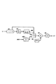
図5は、本発明に従ったイン・バンド・オン・チャネル・デジタル伝送チャネルを組み込み、図1から3を参照しながら上記で説明した変調技法を使用して実施される、FM放送送信機を示すブロック・ダイヤグラムである。図5では、図1に示されたものと同じ構成要素は「図1」とラベル表示された破線の四角形で囲まれ、同じ参照番号が指定されており、以下では詳細に記述していない。エンコーダ10、微分器20、ミキサ30、発振器40、およびBPF50の組合せによって、すべて図1を参照しながら上記で述べたように、デジタル入力信号(図2のNRZ)を表すSSB位相または周波数変調信号(図2のCARR)が生成される。、BPF50の出力端子は増幅器60の入力端子に結合される。増幅器60の出力端子は、第2のミキサ70の第1の入力端子に結合される。第2の発振器80は、第2のミキサ70の第2の入力端子に結合される。第2のミキサ70の出力端子は、第1のフィルタ/増幅器260の入力端子に結合される。第1のフィルタ/増幅器260の出力端子は、信号コンバイナ250の第1の入力端子に結合される。
【0032】
放送ベースバンド信号処理装置210の出力端子は、第3ミキサ220の第1の入力端子に結合される。第3発振器230は、第3ミキサ220の第2の入力端子に結合される。第3ミキサ220の出力端子は、第2のフィルタ/増幅器240の入力端子に結合される。第2のフィルタ/増幅器240の出力端子は、信号コンバイナ250の第2の入力端子に結合される。信号コンバイナ250の出力端子は、伝送アンテナ280に結合された出力増幅器270の入力端子に結合される。
【0033】
オペレーション時には、エンコーダ10がデジタル・オーディオ信号を表すデジタル信号を受け取る。好ましい実施形態では、この信号はMP3準拠のデジタル・オーディオ信号である。より具体的に言えば、デジタル・オーディオデータ・ストリームは、リード・ソロモン(RS)符号を使用して、フォワード・エラー・コレクション(FEC)符号化されている。その後FEC符号化データ・ストリームはパケット化される。その後このパケット化されたデータは、上記で詳細に述べたように、図1に示された回路によってSSB信号に圧縮される。
【0034】
発振器40によって生成される信号の周波数は10.7MHzとなるように選択されるため、エンコーダ10からのデジタル情報は10.7MHzの中心周波数に変調される。変調周波数は任意の周波数であってよいが、より実用的には、既存の低コストBPFフィルタの周波数に対応するように選択される。たとえば、典型的なBPFフィルタは、6MHz、10.7MHz、21.4MHz、70MHz、140MHzなどの中心周波数を有する。例示された実施形態では、変調周波数に10.7MHzが選択され、BPF50は既存の10.7MHzフィルタのうちの1つとして実施される。BPF50からフィルタリングされたSSB信号は増幅器60によって増幅され、第2ミキサ70と第2発振器80の組合せによってアップコンバートされる。例示された実施形態では、第2発振器80が77.57MHzで信号を生成し、SSBは88.27MHzにアップ・コンバートされる。この信号がフィルタリングされ、第1のフィルタ/増幅器260によってさらに増幅される。
【0035】
放送ベースバンド信号処理装置210は、すべて知られた方法で、ステレオ・オーディオ信号(図示せず)を受け取り、ベースバンドでのL+R信号、38kHzの(抑圧)搬送波周波数での両側波帯抑圧搬送波L−R信号、および19kHzのパイロット・トーンを含む、複合ステレオ信号を形成するのに必要な信号処理を実行する。その後この信号は、FM局の割り当てられた周波数で搬送波信号上に変調される。第3発振器230は、例示された実施形態では88.2MHzである割り当てられた放送周波数で、搬送波信号を生成する。第3ミキサ220は、図4bに示されるように、複合モノラルおよびステレオ・オーディオ信号を使用して変調された、変調済み信号を生成する。その後、搬送波周波数88.2MHzの、図4bに示された標準の放送オーディオ側波帯を備えた変調済み信号は、第2のフィルタ/増幅器240によってフィルタリングおよび増幅される。この信号は、第1のフィルタ/増幅器260からのSSB変調済みデジタル信号と組み合わされ、複合信号が形成される。この複合信号には、88.2MHzで搬送波上で変調された標準放送ステレオ・オーディオ側波帯と、図4bに示されるように、搬送波(88.27MHz)より上で70kHzを中心とするデジタル・オーディオ信号を搬送するSSB変調済み信号の、両方を含む。その後この複合信号は、電力増幅器(POWER AMP)270によって電力が増幅され、FMラジオ受信機に伝送するために送信アンテナ280に供給される。
【0036】
図6は、図5に示されたFM放送送信機によって変調された信号を受け取ることのできる、FM放送受信機を示すブロック・ダイヤグラムである。図6では、図3に示されたものと同じ構成要素は「図3」とラベル表示された破線の四角形で囲まれ、同じ参照番号が指定されており、以下では詳細に記述していない。図6では、受信アンテナ302がRF増幅器304に結合される。RF増幅器304の出力端子は第1ミキサ306の第1の入力端子に結合される。第1発振器308の出力端子は第1ミキサ306の第2の入力端子に結合される。第1ミキサ306の出力端子は、BPF310および同調可能BPF110のそれぞれの入力端子に結合される。BFP310の出力端子は、制限増幅器とすることができる中間周波数(IF)増幅器312の入力端子に結合される。IF増幅器312の出力端子は、FM検出器314の入力端子に結合される。FM検出器314の出力端子は、FMステレオデコーダ316の入力端子に結合される。
【0037】
オペレーション時には、RF増幅器304が受信アンテナ304からのRF信号を受け取って増幅する。第1発振器308は、98.9MHzで信号を生成する。第1発振器308と第1ミキサ306の組合せによって、88.2MHzの主搬送波信号を10.7MHzに、88.27MHzからのSSBデジタル・オーディオ信号を10.63MHzにダウン・コンバートする。BPF 310は、知られた方法で、10.7MHzを中心とするFMステレオ信号側波帯(L+RおよびL−R)のみを通過させる。IF増幅器312はこの信号を増幅し、これをベースバンド複合ステレオ信号を生成するFM検出器314に提供する。FMステレオデコーダ316は、すべて知られた方法で、ベースバンド複合ステレオ信号を復号して、伝送されたオーディオ信号を表すモノラルおよび/またはステレオのオーディオ信号(図示せず)を生成する。
【0038】
例示された実施形態では、同調可能BPF110は中心周波数10.63MHzに同調され、その周波数を中心としたデジタル・オーディオ信号のみを通過させる。例示された実施形態では、BPF110の通過帯域は10.53MHzから10.73MHzである。BPF110、積分器120、制限増幅器130、検出器140、デコーダ150、およびウィンドウィング・タイマ160の組合せが、図3を参照しながら上記で述べた方法で、変調済みのデジタル・オーディオ信号を抽出し、その信号を復調および復号して、デジタル・オーディオ信号を再生成する、ように動作する。デコーダ150からのデジタル・オーディオ信号は、伝送されたデジタル・オーディオ信号に対応するオーディオ信号を生成するために、他の回路(図示せず)によって適切な方法で処理される。より具体的に言えば、信号はパケット解除され、伝送中にもたらされた誤りが検出および訂正される。その後、訂正されたビット・ストリームは、すべて知られた方法でステレオ・オーディオ信号に変換される。
【0039】
前述の実施形態は、1024QAMシステムと等価の圧縮性能を提供する。ただし、実際には、配置間隔が狭いこと(tight constellation spacing)により生じるノイズの訂正の困難さ、およびマルチパス・シンボル間干渉(Inter−Symbol Interference;ISI)に起因して、QAMシステムは256QAM周辺に制限される。間隔を広く空けて配置される幅の狭い搬送波パルスによって、上記システムにはISI問題はない。手短に言えば、より高速のデータ・レートで、QAMなどの他の技法に関連付けられた問題なしに、より狭い帯域幅チャネル内を伝送することができる。
【0040】
図2を再度参照すると、CARR信号では、何の搬送波信号も伝送されない、搬送波パルス間のギャップが比較的広いことがわかる。これらのギャップは、本発明に従ったシステムの代替実施形態で利用することができる。図7は、この代替実施形態による変調器のオペレーションを理解するのに役立つCARR信号の、より詳細な波形図である。前述のように、図1に示されたエンコーダでは、符号化クロック信号はNRZ信号のビット周期の9分の1の周期を有する。図7の破線の垂直線は、符号化クロック信号周期を表している。搬送波パルスの許可された時間位置は、破線の四角形で表されている。搬送波パルスは、前の搬送波パルスから8、9、または10クロック・パルス後に発生することができる。したがって搬送波パルスは、3つの隣接するクロック周期のうちいずれか1つで発生することができる。搬送波パルスAは前の搬送波パルスから8クロック・パルスであり、搬送波パルスBは前の搬送波パルスから9クロック・パルスであり、搬送波パルスCは前の搬送波パルスから10クロック・パルスであると想定される。
【0041】
前述のように、搬送波パルスが前の搬送波パルスから8クロック・パルスである(A)場合、これはNRZ信号の後縁(trailing edge)を示し、その直後に続くことのできるのは、NRZ信号に何の変化もないことを表す9クロック・パルス間隔(D)、またはNRZ信号の前縁(leading edge)を表す10クロック・パルス間隔(E)のいずれかのみである。同様に、搬送波パルスが前の搬送波パルスから10クロック・パルスである(C)場合、これはNRZ信号の前縁(leading edge)を示し、その直後に続くことのできるのは、NRZ信号の後縁(trailing edge)を表す8クロック・パルス間隔(E)、またはNRZ信号に何の変化もないことを表す9クロック・パルス間隔(F)のいずれかのみである。搬送波パルスが前の搬送波パルスから9クロック・パルスである(B)場合、これはNRZ信号に何の変化もないことを示し、その直後には、NRZ信号の後縁(trailing edge)を表す8クロック・パルス間隔(D)、NRZ信号に何の変化もないことを表す別の9クロック・パルス間隔(E)、またはNRZ信号の前縁(leading edge)を表す10クロック・パルス間隔(F)のいずれかが続くことができる。これは、図7にすべて図示されている。NRZビット周期中の9つの符号化クロック周期のうち、3つの隣接する周期(t1−t4)のうちの1つは、潜在的に搬送波パルスを有することが可能であるが、他の6つ(t4−t10)は、搬送波パルスを有することができないことは明らかである。
【0042】
CARR信号(時間+4から+10)内に何の搬送波パルスも生成できない間隔中には、搬送波信号上で他の補助データを変調することができる。これは図7で、縦のハッチングを使用した丸みのある四角形(AUX DATA)として示される。最後の潜在的搬送波パルス(C)の後の、およびこのギャップを囲む次に続く潜在的搬送波パルス(D)の前の保護周期(guard period)Δtは、デジタル・オーディオ信号を搬送する搬送波パルス(A)−(F)と補助データを搬送する搬送波変調(AUX DATA)との間の潜在的干渉を最小限にするために維持される。
【0043】
図8は、変調済み復号データ・ストリーム中への補助データの包含を実施できる、本発明の実施形態を示すブロック・ダイヤグラムである。図8では、図1に示されたものと同じ構成要素は同じ参照番号によって指定されており、以下では詳細に記述していない。図8では、補助データ(AUX)の発生源(source)(図示せず)が先入れ先出し(FIFO)バッファ402の入力端子に結合される。FIFOバッファ402の出力端子はマルチプレクサ404の第1のデータ入力端子に結合される。マルチプレクサ404の出力端子は、ミキサ30の入力端子に結合される。レベル検出器25の出力端子は、マルチプレクサ404の第2のデータ入力端子に結合される。エンコーダ10のタイミング信号出力端子は、マルチプレクサ404の制御入力端子に結合される。
【0044】
例示された実施形態では、補助データ信号AUXは搬送波信号を直接変調できる状態にあると想定される。当分野の技術者であれば、その信号の特徴に最も適した方法で搬送波を符号化および/または変調するための信号を準備する方法を理解されよう。さらに、例示された実施形態では、補助データ信号はデジタル形式であると想定される。ただし必ずしもそうである必要はない。補助データ信号はアナログ信号であってもよい。
【0045】
オペレーション時には、エンコーダ10がパルスの相対タイミングを制御する内部タイミング回路(図示せず)を含む。このタイミング回路は、CARR信号においてパルスが潜在的に発生することができるt1からt4の3つの隣接する符号化クロック周期中に第1の状態を有し、t4からt10の残りの符号化クロック周期中に第2の状態を有する信号を生成するために、当分野の技術者であれば理解される方法で、部分修正することができる。この信号は、パルスが発生可能な周期(t1からt4)中には微分器20の出力端子をミキサ30の入力端子に結合し、そうでない場合(のt4からt10中)にはFIFOバッファ402の出力端子をミキサ30に結合するように、マルチプレクサ404を制御するのにに使用することができる。微分器20の出力端子がミキサ30に結合される周期(t1からt4)中は、図8の回路は図1に示された構成であり、上記で詳細に説明したように動作する。
【0046】
(保護帯域Δtを考慮した)FIFOバッファ402がミキサ30に結合される周期(t4+Δtからt10−Δt)中に、FIFOバッファ402からのデータは発振器40からの搬送波信号を変調する。FIFOバッファ402は、一定のビット・レートでデジタル補助データ信号AUXを受け入れ、搬送波パルス(A)−(C)を生成することができる時間周期(t1−t4)中に信号をバッファリングするように動作する。その後FIFOバッファ402は、格納された補助データを、補助データが伝送される時間周期(t4+Δtからt10−Δt)中に、より高速のビット・レートでミキサ30に提供する。CARR信号を介した補助データのバーストのネット・スループットは、補助データ信号発生源(source)(図示せず)からの補助データの一定のネット・スループットと一致しなければならない。当分野の技術者であれば、すべて知られた方法で、スループットを一致させる方法ならびにオーバーランおよびアンダーランに備える方法を理解されよう。
【0047】
図9は、図8に示されたシステムによって生成された信号を受け取ることのできる受信機を示す構成図である。図9では、図3に示されたものと同じ構成要素は同じ参照番号によって指定されており、以下では詳細に記述していない。図9では、検出器140の出力端子が制御可能スイッチ406の入力端子に結合される。制御可能スイッチ406の第1の出力端子は、デコーダ150の入力端子に結合される。制御可能スイッチ406の第2の出力端子は、FIFO408の入力端子に結合される。FIFO408の出力端子は、補助データ(AUX)を生成する。ウィンドウィング・タイマ160の出力端子は、図3のように検出器140のイネーブル入力端子ではなく、制御可能スイッチ406の制御入力端子に結合される。
【0048】
オペレーション時には、図9の検出器140は常に実行可能である。ウィンドウィング・タイマ160からのウィンドウィング信号は、図8のエンコーダ10で生成されるタイミング信号に対応する。ウィンドウィング信号は、搬送波パルス(A)−(C)が潜在的に生じる可能性のある周期(t1からt4)中に第1の状態を有し、そうでない場合(t4からt10)には第2の状態を有する。搬送波パルス(A)−(C)が潜在的に生じる可能性のある周期(t1からt4)中に、ウィンドウィング・タイマ160は、検出器140をデコーダ150に結合するように制御可能スイッチ406を条件付ける。この構成は図3で図示されたものと同一であり、上記で詳細に述べたように動作する。
【0049】
残りのビット周期(t4からt10)中、検出器140はFIFO408に結合される。この周期中、変調済みの補助データは復調され、FIFO408に供給される。(図8の)FIFO402に対応する方法で、FIFO408は検出器140から補助データ・バーストを受け取り、一定のビット・レートで補助データ出力信号AUXを生成する。補助データ信号は補助データを、搬送波を変調するために符号化されたものとして表す。受け取った補助データ信号を所望のフォーマットに復号するために、他の処理(図示せず)が必要になる場合もある。
【図面の簡単な説明】
【図1】
本発明に従ったFM放送システムで使用可能な変調器のブロック・ダイヤグラムである。
【図2】
図1に示された変調器のオペレーションを理解するのに役立つ波形図である。
【図3】
図1に示された変調器に従って変調された信号を受け取ることのできる受信機のブロック・ダイヤグラムである。
【図4】
本発明に従った図1および2に示された変調技法の適用を理解するのに役立つスペクトル図である。
【図5】
本発明に従ったイン・バンド・オン・チャネル・デジタル伝送チャネルを組み込んだ、FM放送送信機のブロック・ダイヤグラムである。
【図6】
図5に示されたFM放送送信機によって変調された信号を受け取ることのできる本発明に従ったFM放送受信機のブロック・ダイヤグラムである。
【図7】
本発明で使用できる変調器の他の実施形態のオペレーションを理解するのに役立つ波形図である。
【図8】
本発明で使用できる変調器の他の実施形態のブロック・ダイヤグラムである。
【図9】
図8に示されたシステムによって生成された信号を受け取ることのできる、本発明で使用可能な受信機の他の実施形態のブロック・ダイヤグラムである。[0001]
The present invention relates to modulation techniques for providing high data rates over band limited channels, and more particularly to in-band on-channel for digital data, especially digital audio. (IBOC) FM broadcast modulation system.
[0002]
In the United States, FM broadcasters provide full power in sidebands within 100 kHz of their assigned carrier frequency and full power in sidebands within a frequency range of 100 kHz to 200 kHz around the carrier. Information can be transmitted with an output that is 30 dB lower than that of the information. Standard stereo audio signals are placed in a bandwidth within 53 kHz from the carrier. Thus, the broadcaster can transmit other information in the remaining bandwidth, subject to the above restrictions.
[0003]
It has become desirable for FM broadcasting companies to simultaneously broadcast stereo audio data and digital data. For example, the digital data can represent a high quality version of the stereo audio being broadcast. This requires a relatively fast data rate channel, which is limited to a relatively narrow bandwidth. For example, a digital data stream that carries high quality audio may have a bit rate of 128 kilobits per second (KBPS). A signal carrying such a data stream cannot be transmitted over the bandwidth available in an FM broadcast signal without using some form of compression to reduce the bandwidth required for the signal.
[0004]
It is always desirable to provide data at high data rates over bandwidth limited channels. Many modulation techniques have been developed to increase the data rate over the channel. For example, M-ary phase shift keyed (PSK) and quadrature amplitude modulation (QAM) techniques compress compression by encoding multiple data bits in each transmitted symbol (symbol). enable. These systems have limitations associated with them. First, the hardware associated with such systems is expensive. This is because these techniques require a high level of channel linearity to work properly. Therefore, extensive signal processing must be performed for carrier tracking, symbol recovery, interpolation, and signal shaping. Second, such techniques are sensitive to multipath effects. These effects need to be compensated for in the receiver. Third, these systems require more bandwidth than is available in some applications (eg, in-band on-channel broadcast FM sub-carrier services) to achieve the desired data rate Often.
[0005]
In accordance with the principles of the present invention, an FM broadcast transmitter transmits a broadcast signal having a broadcast frequency carrier and sidebands and is capable of transmitting at full power within a transmission bandwidth around the carrier. This includes a source of a modulated FM stereo signal having a carrier at the broadcast frequency and having sidebands with a narrower bandwidth than the transmission bandwidth representing the stereo signal. Further, a carrier pulse, spaced apart from one another, representing an IBOC digital data signal encoded as a variable pulse width encoded signal, and a non-overlapping transmission of FM stereo signal sidebands. A source of the modulated IBOC signal having a bandwidth within the bandwidth is also included. The signal combiner combines the modulated FM stereo signal and the modulated IBOC signal to form a broadcast signal.
[0006]
According to another aspect of the invention, an FM broadcast receiver includes a first modulated signal representing an FM stereo signal and an in-band on channel (IBOC) digital signal encoded as a variable pulse width encoded signal. Receiving a broadcast signal comprising a data signal and a second modulated signal having carrier pulses spaced relative to each other. The FM broadcast receiver includes a signal separator for generating a first separated signal representing an FM stereo signal and a second separated signal representing an IBOC digital data signal. The FM signal processing device generates a stereo audio signal represented by the FM stereo signal. The IBOC signal processor generates a digital data signal represented by the IBOC digital data signal.
[0007]
Techniques in accordance with the principles of the present invention provide an FM transmission system that includes a second channel that carries a relatively high data rate digital signal. This channel is located in a portion of the FM bandwidth that can be transmitted at full power. The circuitry required to implement such a channel is relatively simple and inexpensive. Furthermore, it does not require high channel linearity and is not subject to multipath problems. The additional circuitry required to implement this channel in the receiver is relatively small and can be coupled to the output of an IF circuit pre-existing in the receiver.
[0008]
FIG. 1 is a block diagram of a modulator that can be used in the present invention. In FIG. 1, the input terminal IN receives a digital signal. Input terminal IN is coupled to an input terminal of
[0009]
FIG. 2 is a waveform diagram useful in understanding the operation of the modulator shown in FIG. FIG. 2 is not drawn to scale the waveform more clearly as illustrated. In the illustrated embodiment, the digital signal at input terminal IN is a two-layer signal in non-return-to-zero (NRZ) format. This signal is shown as the top waveform in FIG. The NRZ signal carries successive bits, each of which lasts for a predetermined period called the bit period indicated by the dashed line in the NRZ signal and has a corresponding frequency called the bit rate. In all known methods, the level of the NRZ signal represents the value of that bit.
[0010]
Each bit period of the NRZ signal is coded as a transition of the coded signal. An encoding clock at a multiple M of the bit rate is used to phase encode the NRZ signal. In the above-mentioned patent application, the encoding clock operates at a rate M which is nine times the bit rate. When the NRZ signal transitions from a logic "1" level to a logic "0" level, the transition is performed in the encoded signal 8 encoded clock cycles (M-1) from the previous transition. When the NRZ signal transitions from a logic "0" level to a logic "1" level, the transition is performed in the encoded
[0011]
The variable aperture coded signal (VAC) is differentiated by
[0012]
(Equation 1)
![]()
Is shown as the third signal in FIG.
[0014]
(Equation 2)
![]()
Is level-detected by the
[0016]
[Equation 3]
![]()
Has a value greater than a positive threshold, the level signal is generated with a high value, and if it has a value less than a negative threshold, the level signal is a lower value (low). value), otherwise it has a center value. The level signal is shown as a fourth signal (LEVEL) in FIG.
[0018]
The LEVEL signal modulates the carrier signal from the
[0019]
The
[0020]
FIG. 3 is a block diagram of a receiver capable of receiving a signal modulated as shown in FIG. In FIG. 3, input terminal IN is coupled to a source of a signal modulated as described above with reference to FIGS. Input terminal IN is coupled to the input terminal of
[0021]
In operation, the
[0022]
The carrier pulses (the signal CARR in FIG. 2) occur at distinct times and, due to their limited duration, enable the
[0023]
3 has an input terminal coupled to the status output terminal of the
[0024]
In the illustrated embodiment, the energy in the modulated signal is primarily between 0.44 (8/18) and 0.55 (10/18) times the bit rate and therefore the bit rate It has 0.11 times the bandwidth. As a result, the data rate over the bandwidth increases nine-fold. Other compression ratios are easily achieved by varying the coding clock to bit rate ratio, due to trade-offs and constraints that will be readily understood by those skilled in the art. You.
[0025]
The above-described system can be implemented with less sophisticated circuitry than either M-ary PSK or QAM modulation techniques at both the transmitter and the receiver. More specifically, the receiver can use a less expensive and power saving limiting amplifier (eg, 130) compared to
[0026]
As mentioned above, the carrier transmission occurs only on bit boundaries and does not last for the entire bit period, so a time window is established in the receiver to detect the received carrier pulse only when the pulse is expected. Can be used. Therefore, there is no multi-path problems in the system.
[0027]
In accordance with the principles of the present invention, the above-described modulation technique is used when simultaneously transmitting an FM mono broadcast audio signal and a stereo broadcast audio signal of an FM broadcast signal and digital data (eg, CD quality digital music). used. FIG. 4 is a spectral diagram that is helpful in understanding the application of the modulation techniques shown in FIGS. 1 and 2 to a system according to the present invention. FIG. 4a is a diagram illustrating a power envelope for an FM broadcast signal in the United States. In FIG. 4a, the horizontal lines represent frequency and represent a portion of the VHF band around between approximately 88 MHz and 107 MHz. The signal strength is represented in the vertical direction. The allowed envelope of two adjacent broadcast signal spectra is shown. Each carrier is illustrated by a vertical arrow. Around each carrier is a sideband that carries a broadcast signal FM modulated by the carrier.
[0028]
In the United States, FM radio stations can broadcast mono and stereo audio at full power in sidebands within the 100 kHz range of the carrier. In FIG. 4a, these sidebands are shown without hatching. Broadcasters can broadcast other information in the sideband from 100 kHz to 200 kHz, but the power transmitted within this band must be 30 dB below full power. These sidebands are illustrated by hatching. Neighbor stations (within the same geographic area) must be at least 400 kHz apart.
[0029]
The upper side-band of the carrier of the lower frequency broadcast signal in FIG. 4a is illustrated in the lower spectral diagram of FIG. 4b. In FIG. 4b, the vertical direction represents the modulation rate. In FIG. 4b, the monaural audio signal L + R audio signal is transmitted at a modulation level of 90% in the sideband from 0 to 15 kHz. The LR audio signal is transmitted at a modulation level of 45% as a double sideband suppressed carrier signal centered on a suppressed subcarrier frequency of 38 kHz. The lower sideband (lsb) ranges from 23 kHz to 38 kHz, and the upper sideband (usb) ranges from 38 kHz to 53 kHz. The 19 kHz pilot tone (half the frequency of the suppressed carrier) is also included in the sideband centered on the main carrier. Thus, in both the upper sideband (FIG. 4b) and the lower sideband (not shown) centered on the main carrier, 47 kHz is still used by broadcasters to broadcast additional information at full power. It remains possible. As mentioned above, the transmission power from 100 kHz to 200 kHz must be 30 dB below full power.
[0030]
Using the modulation techniques shown in FIGS. 1 and 2 above, a 128 kilobits per second (KBPS) signal containing an MP3 CD quality audio signal can be transmitted compressed with a bandwidth of less than 20 kHz. . This digital audio signal can be located between 53 kHz and 100 kHz in the upper sideband (for example) and transmitted as a subcarrier signal along with a normal broadcast stereo audio signal, as shown in FIG. 4b. In FIG. 4b, the digital audio signal is the aforementioned SSB signal centered at approximately 70 kHz, ranging from approximately 60 kHz to 80 kHz. Since this signal is within the 100 kHz range of the main carrier, it can be transmitted at full power. These signals are called in-band-on-channel (IBOC) signals.
[0031]
FIG. 5 illustrates an FM broadcast transmitter incorporating an in-band on-channel digital transmission channel according to the present invention and implemented using the modulation techniques described above with reference to FIGS. It is a block diagram shown. In FIG. 5, the same components as those shown in FIG. 1 are surrounded by a dashed rectangle labeled "FIG. 1" and have the same reference numbers designated, and are not described in detail below. The combination of the
[0032]
An output terminal of the broadcast baseband
[0033]
In operation, the
[0034]
Since the frequency of the signal generated by
[0035]
The broadcast
[0036]
FIG. 6 is a block diagram showing an FM broadcast receiver capable of receiving a signal modulated by the FM broadcast transmitter shown in FIG. In FIG. 6, the same components as those shown in FIG. 3 are surrounded by a dashed rectangle labeled "FIG. 3" and have the same reference numbers designated therein, and are not described in detail below. In FIG. 6, the receiving
[0037]
In operation, the
[0038]
In the illustrated embodiment, the
[0039]
The above embodiments provide compression performance equivalent to a 1024 QAM system. However, in practice, the QAM system has a 256 QAM area due to difficulties in correcting noise caused by a narrow constellation spacing (interval-symbol interference; ISI). Is limited to With narrowly spaced carrier pulses spaced widely, there is no ISI problem in the system. Briefly, higher data rates can be transmitted within a narrower bandwidth channel without the problems associated with other techniques such as QAM.
[0040]
Referring again to FIG. 2, it can be seen that in the CARR signal, no carrier signal is transmitted and the gap between carrier pulses is relatively wide. These gaps can be used in alternative embodiments of the system according to the invention. FIG. 7 is a more detailed waveform diagram of the CARR signal that helps to understand the operation of the modulator according to this alternative embodiment. As described above, in the encoder shown in FIG. 1, the encoded clock signal has a period that is 1/9 of the bit period of the NRZ signal. The dashed vertical line in FIG. 7 represents the encoded clock signal period. The allowed time position of the carrier pulse is represented by a dashed square. The carrier pulse can occur 8, 9, or 10 clock pulses after the previous carrier pulse. Thus, the carrier pulse can occur at any one of three adjacent clock periods. Carrier pulse A is assumed to be 8 clock pulses from the previous carrier pulse, carrier pulse B is assumed to be 9 clock pulses from the previous carrier pulse, and carrier pulse C is assumed to be 10 clock pulses from the previous carrier pulse. You.
[0041]
As mentioned above, if the carrier pulse is 8 clock pulses from the previous carrier pulse (A), this indicates a trailing edge of the NRZ signal, which can immediately follow the NRZ signal. There is only either a 9 clock pulse interval (D) representing no change in the NRZ signal, or a 10 clock pulse interval (E) representing the leading edge of the NRZ signal. Similarly, if the carrier pulse is 10 clock pulses from the previous carrier pulse (C), this indicates the leading edge of the NRZ signal, which can immediately follow the NRZ signal. There are only either 8 clock pulse intervals (E), representing the trailing edge, or 9 clock pulse intervals (F), representing no change in the NRZ signal. If the carrier pulse is 9 clock pulses from the previous carrier pulse (B), this indicates that there is no change in the NRZ signal, immediately followed by a trailing edge 8 representing the NRZ signal. Clock pulse interval (D), another 9 clock pulse intervals (E), indicating no change in the NRZ signal, or 10 clock pulse intervals (F), indicating the leading edge of the NRZ signal. Either can follow. This is all illustrated in FIG. Of the nine coded clock periods in the NRZ bit period, one of three adjacent periods (t1-t4) can potentially have carrier pulses, while the other six ( It is clear that t4-t10) cannot have a carrier pulse.
[0042]
During the intervals during which no carrier pulse can be generated in the CARR signal (time +4 to +10), other auxiliary data can be modulated on the carrier signal. This is shown in FIG. 7 as a rounded square (AUX DATA) using vertical hatching. The guard period Δt after the last potential carrier pulse (C) and before the next potential carrier pulse (D) surrounding this gap is the carrier period (t) that carries the digital audio signal. A)-(F) are maintained to minimize potential interference between the carrier modulation (AUX DATA) carrying the auxiliary data.
[0043]
FIG. 8 is a block diagram illustrating an embodiment of the present invention in which the inclusion of ancillary data in a modulated decoded data stream may be implemented. 8, the same components as those shown in FIG. 1 are designated by the same reference numerals, and are not described in detail below. In FIG. 8, a source (not shown) of auxiliary data (AUX) is coupled to an input terminal of a first-in first-out (FIFO)
[0044]
In the illustrated embodiment, it is assumed that the auxiliary data signal AUX is ready to directly modulate the carrier signal. Those skilled in the art will understand how to prepare a signal to encode and / or modulate a carrier in a manner that best suits the characteristics of the signal. Further, in the illustrated embodiment, the auxiliary data signal is assumed to be in digital form. However, this need not be the case. The auxiliary data signal may be an analog signal.
[0045]
In operation, the
[0046]
During the period (t4 + Δt to t10−Δt) in which the
[0047]
FIG. 9 is a block diagram illustrating a receiver that can receive a signal generated by the system illustrated in FIG. In FIG. 9, the same components as those shown in FIG. 3 are designated by the same reference numerals, and are not described in detail below. In FIG. 9, the output terminal of
[0048]
In operation, the
[0049]
During the remaining bit periods (t4 to t10),
[Brief description of the drawings]
FIG.
3 is a block diagram of a modulator usable in an FM broadcasting system according to the present invention.
FIG. 2
FIG. 2 is a waveform diagram useful for understanding the operation of the modulator shown in FIG. 1.
FIG. 3
2 is a block diagram of a receiver capable of receiving a signal modulated according to the modulator shown in FIG.
FIG. 4
FIG. 3 is a spectral diagram useful in understanding the application of the modulation technique shown in FIGS. 1 and 2 in accordance with the present invention.
FIG. 5
1 is a block diagram of an FM broadcast transmitter incorporating an in-band on-channel digital transmission channel according to the present invention.
FIG. 6
6 is a block diagram of an FM broadcast receiver according to the present invention capable of receiving a signal modulated by the FM broadcast transmitter shown in FIG. 5.
FIG. 7
FIG. 4 is a waveform diagram useful in understanding the operation of another embodiment of a modulator that can be used with the present invention.
FIG. 8
5 is a block diagram of another embodiment of a modulator that can be used in the present invention.
FIG. 9
9 is a block diagram of another embodiment of a receiver usable with the present invention that can receive signals generated by the system shown in FIG.
Claims (28)
前記放送周波数での搬送波を有し、ステレオ信号を表す、前記伝送帯域幅よりも狭い帯域幅を備えた側波帯を有する変調FMステレオ信号の発生源(210、220、230、240)と、
可変パルス幅符号化信号として符号化されたIBOCデジタル・データ信号を表す、互いを基準として間隔を空けて配置された搬送波パルスと、前記FMステレオ信号側波帯と重複することのない、前記伝送帯域幅内の帯域幅を有する変調IBOC信号の発生源(10、20、25、30−80、260)と、
前記変調FMステレオ信号と前記変調IBOC信号を組み合わせて前記放送信号を形成するための信号コンバイナ(250)と
によって特徴付けられるFM放送送信機。An FM broadcast transmitter capable of transmitting at full power within a transmission bandwidth centered on the carrier, for transmitting a broadcast signal having a carrier wave and a sideband of a broadcast frequency,
A source (210, 220, 230, 240) of a modulated FM stereo signal having a carrier at the broadcast frequency and having a sideband with a bandwidth narrower than the transmission bandwidth, representing a stereo signal;
A carrier pulse, spaced apart from each other, representing an IBOC digital data signal encoded as a variable pulse width encoded signal, and the transmission not overlapping with the FM stereo signal sideband. Sources of modulated IBOC signals having a bandwidth within the bandwidth (10, 20, 25, 30-80, 260);
An FM broadcast transmitter characterized by a signal combiner (250) for combining the modulated FM stereo signal and the modulated IBOC signal to form the broadcast signal.
ステレオ・オーディオ信号に応答して複合ステレオ信号を生成するための信号処理装置(210)と、
前記放送周波数搬送波上で前記複合ステレオ信号を変調するための変調器(220、230)と
を備えることに特徴付けられる請求項1に記載の送信機。The modulated stereo signal source,
A signal processing device (210) for generating a composite stereo signal in response to the stereo audio signal;
The transmitter according to claim 1, characterized by comprising a modulator (220, 230) for modulating the composite stereo signal on the broadcast frequency carrier.
前記放送周波数搬送波信号を生成する発振器(230)と、
前記FMステレオ信号を生成する、前記発振器および前記信号処理装置(210)に結合されたミキサ(220)と
を備えることに特徴付けられる請求項3に記載の送信機。The modulator is
An oscillator (230) for generating the broadcast frequency carrier signal;
The transmitter according to claim 3, characterized in that it comprises a mixer (220) coupled to the oscillator and the signal processing device (210) for generating the FM stereo signal.
前記IBOCデジタル・データ信号の発生源と、
可変パルス幅コードを使用して前記デジタル・データを符号化するためのエンコーダ(10)と、
前記符号化デジタル・データ信号の縁部(edge)を表すそれぞれのパルスを生成するパルス信号生成器(20、25)と、
前記それぞれのパルスに対応する搬送波パルスを有する搬送波信号を生成する搬送波パルス信号生成器(30−80)と
を備えることに特徴付けられる請求項1に記載の送信機。The modulated IBOC signal source comprises:
A source of the IBOC digital data signal;
An encoder (10) for encoding the digital data using a variable pulse width code;
Pulse signal generators (20, 25) for generating respective pulses representing edges of the encoded digital data signal;
The transmitter according to claim 1, further comprising a carrier pulse signal generator (30-80) for generating a carrier signal having a carrier pulse corresponding to each of the pulses.
前記パルス信号に応答して中間周波数パルス信号を生成する第1の変調器(30、40)と、
前記中間周波数搬送波信号を前記搬送波パルス信号にアップ・コンバートする第2の変調器(70、80)と
を備えることに特徴付けられる請求項6に記載の送信機。The carrier pulse signal generator,
A first modulator (30, 40) for generating an intermediate frequency pulse signal in response to the pulse signal;
7. The transmitter according to claim 6, comprising a second modulator (70, 80) for up-converting the intermediate frequency carrier signal to the carrier pulse signal.
前記第2の変調器は、前記FMステレオ信号側波帯と重複することのない、前記伝送帯域幅内に前記搬送波パルス信号を配置するための、周波数で搬送波信号を生成する第2の発振器(80)と、前記搬送波パルス信号を生成する、前記第1の変調器および前記第2の発振器に結合された第2のミキサ(70)とを備える
ことに特徴付けられる請求項7に記載の送信機。The first modulator is coupled to a first oscillator (40) for generating a carrier signal at the intermediate frequency, and to the pulse signal generator and the first oscillator for generating the intermediate frequency pulse signal. , A first mixer (30),
A second oscillator that generates a carrier signal at a frequency for arranging the carrier pulse signal within the transmission bandwidth without overlapping with the FM stereo signal sideband; 80) and a second mixer (70) coupled to the first modulator and the second oscillator for generating the carrier pulse signal. Machine.
前記パルス信号生成器(20、25)は、前記デジタル・データ信号の前記前縁および後縁のうちの一方に応答して正のパルスを生成し、前記デジタル・データ信号の前記前縁および後縁のうちの他方に応答して負のパルスを生成すること、および
前記搬送波信号生成器(30−80)は、正のパルスに応答して第1の位相を有し、負のパルスに応答して第2の位相を有する、搬送波パルスを生成すること
に特徴付けられる請求項6に記載の送信機。Said encoder (10) generates an encoded digital data signal having a leading edge and a trailing edge;
The pulse signal generator (20, 25) generates a positive pulse in response to one of the leading edge and the trailing edge of the digital data signal, and the leading and trailing edges of the digital data signal. Generating a negative pulse in response to the other of the edges; and the carrier signal generator (30-80) having a first phase in response to a positive pulse and responsive to a negative pulse The transmitter according to claim 6, characterized in that the transmitter generates a carrier pulse having a second phase.
前記エンコーダに結合された微分器(20)と、
前記微分器に結合されたレベル検出器(25)と
を備えることに特徴付けられる請求項に記載の送信機。The pulse signal generator,
A differentiator (20) coupled to the encoder;
Transmitter according to claim 10, characterized in that it comprises a level detector (25) coupled to the differentiator.
前記放送信号に応答して、FMステレオ信号を表す第1の分離された信号と、IBOCデジタル・データ信号を表す第2の分離された信号とを生成する信号セパレータ(310、110)と、
前記第1の分離された信号に応答して、前記FMステレオ信号によって表されるステレオ・オーディオ信号を生成するFM信号処理装置(310、312、314、316)と、
前記第2の分離された信号に応答して、前記IBOCデジタル・データ信号によって表されるデジタル・データ信号を生成するIBOC信号処理装置(120、130、140、150、160)とに特徴付けられるFM放送受信機。A first modulated signal representing an FM stereo signal and an in-band-on-channel (IBOC) digital data signal encoded as a variable pulse width encoded signal, spaced apart from each other An FM broadcast receiver for receiving a broadcast signal including a second modulated signal having a carrier pulse.
A signal separator (310, 110) responsive to the broadcast signal for generating a first separated signal representing an FM stereo signal and a second separated signal representing an IBOC digital data signal;
An FM signal processor (310, 312, 314, 316) for generating a stereo audio signal represented by the FM stereo signal in response to the first separated signal;
An IBOC signal processor (120, 130, 140, 150, 160) for generating a digital data signal represented by the IBOC digital data signal in response to the second separated signal. FM broadcast receiver.
前記第1の分離された信号のみを渡すための第1の帯域フィルタ(310)と、
前記第2の分離された信号のみを渡すための第2の帯域フィルタ(110)と
を備えることに特徴付けられる請求項16に記載の受信機。The signal separator,
A first bandpass filter (310) for passing only said first separated signal;
The receiver according to claim 16, characterized in that it comprises a second bandpass filter (110) for passing only the second separated signal.
ローカル発振器(308)と、
前記ローカル発振器に結合され、前記放送信号に応答して前記放送信号を中間周波数に変換するためのミキサ(306)と
を備えることに特徴付けられる請求項19に記載の受信機。The down converter includes:
A local oscillator (308);
20. The receiver of claim 19, further comprising: a mixer coupled to the local oscillator for converting the broadcast signal to an intermediate frequency in response to the broadcast signal.
前記第2の分離された信号に応答するFM検出器(314)と、
前記FM検出器(314)に結合された、前記ステレオ・オーディオ信号を生成するためのFMステレオデコーダ(316)と
を備えることに特徴つけられる請求項16に記載の受信機。The FM signal processing device includes:
An FM detector (314) responsive to the second separated signal;
The receiver of claim 16, comprising an FM stereo decoder (316) coupled to the FM detector (314) for generating the stereo audio signal.
前記第2の分離された信号に応答する、受け取った搬送波パルスに応答して可変パルス幅符号化信号を生成する検出器(140)と、
前記可変パルス幅符号化信号を復号し、前記デジタル・データ信号を生成するデコーダ(150)と
を備えることに特徴付けられる請求項16に記載の受信機。The IBOC signal processing device comprises:
A detector (140) responsive to the received carrier pulse for generating a variable pulse width coded signal responsive to the second separated signal;
17. The receiver according to claim 16, comprising a decoder (150) for decoding the variable pulse width coded signal and generating the digital data signal.
Applications Claiming Priority (2)
| Application Number | Priority Date | Filing Date | Title |
|---|---|---|---|
| US09/626,295 US6792051B1 (en) | 2000-07-25 | 2000-07-25 | In-band-on-channel broadcast system for digital data |
| PCT/US2001/022850 WO2002009329A2 (en) | 2000-07-25 | 2001-07-20 | An in-band-on-channel broadcast system for digital data |
Publications (3)
| Publication Number | Publication Date |
|---|---|
| JP2004509487A true JP2004509487A (en) | 2004-03-25 |
| JP2004509487A5 JP2004509487A5 (en) | 2008-09-18 |
| JP4651910B2 JP4651910B2 (en) | 2011-03-16 |
Family
ID=24509787
Family Applications (1)
| Application Number | Title | Priority Date | Filing Date |
|---|---|---|---|
| JP2002514930A Expired - Fee Related JP4651910B2 (en) | 2000-07-25 | 2001-07-20 | In-band on-channel broadcasting system for digital data |
Country Status (11)
| Country | Link |
|---|---|
| US (2) | US6792051B1 (en) |
| EP (1) | EP1314269B1 (en) |
| JP (1) | JP4651910B2 (en) |
| KR (1) | KR100811570B1 (en) |
| CN (1) | CN1529957B (en) |
| AU (2) | AU7793101A (en) |
| BR (1) | BR0112742A (en) |
| MX (1) | MXPA03000758A (en) |
| MY (1) | MY128804A (en) |
| SG (1) | SG144728A1 (en) |
| WO (1) | WO2002009329A2 (en) |
Cited By (3)
| Publication number | Priority date | Publication date | Assignee | Title |
|---|---|---|---|---|
| JP2004505506A (en) * | 2000-07-25 | 2004-02-19 | トムソン ライセンシング ソシエテ アノニム | Data transmission using pulse width modulation |
| JP2004510362A (en) * | 2000-07-25 | 2004-04-02 | トムソン ライセンシング ソシエテ アノニム | Data transmission using palace width modulation |
| JP2017005580A (en) * | 2015-06-12 | 2017-01-05 | 株式会社東芝 | Transmitter |
Families Citing this family (9)
| Publication number | Priority date | Publication date | Assignee | Title |
|---|---|---|---|---|
| US7502355B2 (en) * | 2005-03-04 | 2009-03-10 | Cisco Technology, Inc. | Adaptive multiplexing device for multi-carrier wireless telecommunication systems |
| US7656957B2 (en) * | 2005-06-24 | 2010-02-02 | Cisco Technology, Inc. | Multiplexing system for time division duplex communication systems |
| EP1772980A1 (en) * | 2005-10-06 | 2007-04-11 | Delphi Technologies, Inc. | Method and apparatus for for the transmission of broadcasts |
| WO2008021305A2 (en) * | 2006-08-10 | 2008-02-21 | Sirius Satellite Radio Inc. | Methods and systems for retransmission of a broadcast signal using a proximity transmitting radiator |
| US7945225B2 (en) * | 2007-07-09 | 2011-05-17 | Myat, Inc. | Medium loss high power IBOC combiner |
| US20090310786A1 (en) * | 2008-06-11 | 2009-12-17 | Quintic Holdings | Systems for Channel Coordination of Audio and Data Transmission in a Broadcast Band |
| US8392613B2 (en) * | 2008-07-03 | 2013-03-05 | Nokia Corporation | Network address assignment |
| CN101778064B (en) * | 2009-01-13 | 2013-05-22 | 财团法人工业技术研究院 | Transmitter for processing peak to average power ratio and method thereof |
| JP6149937B2 (en) * | 2013-10-02 | 2017-06-21 | 富士通株式会社 | Pulse position modulation type impulse radio transmitter and radio communication system |
Citations (3)
| Publication number | Priority date | Publication date | Assignee | Title |
|---|---|---|---|---|
| WO1997039544A1 (en) * | 1996-04-17 | 1997-10-23 | Lockheed Martin Corporation | Method for digital broadcasting over the commercial fm band |
| JP2001520479A (en) * | 1997-10-09 | 2001-10-30 | アイビキュイティ・デジタル・コーポレイション | System and method for mitigating intermittent interruptions in audio radio broadcasts |
| JP2002507075A (en) * | 1998-03-11 | 2002-03-05 | トムソン ライセンシング ソシエテ アノニム | Digital signal modulation system |
Family Cites Families (14)
| Publication number | Priority date | Publication date | Assignee | Title |
|---|---|---|---|---|
| US4408166A (en) * | 1980-12-29 | 1983-10-04 | Altex Scientific, Inc. | Pulse width modulation decoder |
| FR2688332B1 (en) * | 1992-03-03 | 1995-12-01 | Thomson Csf | METHOD AND DEVICE FOR RECORDING READING OF INFORMATION ON A MOBILE OPTICAL OR MAGNETO-OPTICAL MEDIUM. |
| US5465396A (en) | 1993-01-12 | 1995-11-07 | Usa Digital Radio Partners, L.P. | In-band on-channel digital broadcasting |
| US5757864A (en) * | 1995-08-17 | 1998-05-26 | Rockwell Semiconductor Systems, Inc. | Receiver with filters offset correction |
| US5949796A (en) | 1996-06-19 | 1999-09-07 | Kumar; Derek D. | In-band on-channel digital broadcasting method and system |
| US6430227B1 (en) * | 1998-03-27 | 2002-08-06 | Ibiquity Digital Corporation | FM in-band-on-channel digital audio broadcasting method and system |
| US6486776B1 (en) * | 1998-04-14 | 2002-11-26 | The Goodyear Tire & Rubber Company | RF transponder and method of measuring parameters associated with a monitored object |
| EP1011203B1 (en) | 1998-06-09 | 2009-08-12 | Sony Corporation | Receiver and method of reception |
| US6590944B1 (en) * | 1999-02-24 | 2003-07-08 | Ibiquity Digital Corporation | Audio blend method and apparatus for AM and FM in band on channel digital audio broadcasting |
| US7085377B1 (en) | 1999-07-30 | 2006-08-01 | Lucent Technologies Inc. | Information delivery in a multi-stream digital broadcasting system |
| US6549544B1 (en) * | 1999-11-10 | 2003-04-15 | Ibiquity Digital Corporation | Method and apparatus for transmission and reception of FM in-band on-channel digital audio broadcasting |
| US6359525B1 (en) * | 2000-07-25 | 2002-03-19 | Thomson Licensing S.A. | Modulation technique for transmitting multiple high data rate signals through a band limited channel |
| JP2008001004A (en) * | 2006-06-23 | 2008-01-10 | Canon Inc | Manufacturing method of liquid feeding part of liquid storage container and liquid storage container |
| JP4873139B2 (en) * | 2006-06-23 | 2012-02-08 | Nok株式会社 | Manufacturing method of gasket |
-
2000
- 2000-07-25 US US09/626,295 patent/US6792051B1/en not_active Expired - Fee Related
-
2001
- 2001-07-20 SG SG200407619-6A patent/SG144728A1/en unknown
- 2001-07-20 MX MXPA03000758A patent/MXPA03000758A/en active IP Right Grant
- 2001-07-20 BR BR0112742-0A patent/BR0112742A/en not_active IP Right Cessation
- 2001-07-20 KR KR1020037001100A patent/KR100811570B1/en not_active IP Right Cessation
- 2001-07-20 AU AU7793101A patent/AU7793101A/en active Pending
- 2001-07-20 EP EP01955880A patent/EP1314269B1/en not_active Expired - Lifetime
- 2001-07-20 CN CN018146449A patent/CN1529957B/en not_active Expired - Fee Related
- 2001-07-20 JP JP2002514930A patent/JP4651910B2/en not_active Expired - Fee Related
- 2001-07-20 WO PCT/US2001/022850 patent/WO2002009329A2/en active IP Right Grant
- 2001-07-20 AU AU2001277931A patent/AU2001277931B2/en not_active Ceased
- 2001-07-23 MY MYPI20013478A patent/MY128804A/en unknown
-
2004
- 2004-08-04 US US10/912,250 patent/US7388911B2/en not_active Expired - Fee Related
Patent Citations (3)
| Publication number | Priority date | Publication date | Assignee | Title |
|---|---|---|---|---|
| WO1997039544A1 (en) * | 1996-04-17 | 1997-10-23 | Lockheed Martin Corporation | Method for digital broadcasting over the commercial fm band |
| JP2001520479A (en) * | 1997-10-09 | 2001-10-30 | アイビキュイティ・デジタル・コーポレイション | System and method for mitigating intermittent interruptions in audio radio broadcasts |
| JP2002507075A (en) * | 1998-03-11 | 2002-03-05 | トムソン ライセンシング ソシエテ アノニム | Digital signal modulation system |
Non-Patent Citations (1)
| Title |
|---|
| JPN6010043981, R. L. Cupo, M. Sarraf, M. Shariat and M. Zarrabizadeh, "An OFDM All Digital In−Band−On−Channel (IBOC) AM and FM Radio Solution Using the PAC Encoder", IEEE Transactions on Broadcasting, 199803, 第44巻, 第1号, p.22−26 * |
Cited By (4)
| Publication number | Priority date | Publication date | Assignee | Title |
|---|---|---|---|---|
| JP2004505506A (en) * | 2000-07-25 | 2004-02-19 | トムソン ライセンシング ソシエテ アノニム | Data transmission using pulse width modulation |
| JP2004510362A (en) * | 2000-07-25 | 2004-04-02 | トムソン ライセンシング ソシエテ アノニム | Data transmission using palace width modulation |
| JP4745593B2 (en) * | 2000-07-25 | 2011-08-10 | トムソン ライセンシング | Data transmission using palace width modulation |
| JP2017005580A (en) * | 2015-06-12 | 2017-01-05 | 株式会社東芝 | Transmitter |
Also Published As
| Publication number | Publication date |
|---|---|
| MXPA03000758A (en) | 2003-06-04 |
| CN1529957A (en) | 2004-09-15 |
| KR20030064735A (en) | 2003-08-02 |
| BR0112742A (en) | 2004-06-08 |
| MY128804A (en) | 2007-02-28 |
| JP4651910B2 (en) | 2011-03-16 |
| US6792051B1 (en) | 2004-09-14 |
| CN1529957B (en) | 2010-06-16 |
| SG144728A1 (en) | 2008-08-28 |
| EP1314269A2 (en) | 2003-05-28 |
| AU2001277931C1 (en) | 2002-02-05 |
| EP1314269B1 (en) | 2012-11-21 |
| US20050009478A1 (en) | 2005-01-13 |
| AU2001277931B2 (en) | 2005-12-01 |
| WO2002009329A3 (en) | 2003-03-27 |
| WO2002009329A2 (en) | 2002-01-31 |
| KR100811570B1 (en) | 2008-10-27 |
| AU7793101A (en) | 2002-02-05 |
| US7388911B2 (en) | 2008-06-17 |
Similar Documents
| Publication | Publication Date | Title |
|---|---|---|
| US6359525B1 (en) | Modulation technique for transmitting multiple high data rate signals through a band limited channel | |
| JP4798931B2 (en) | Transmission of primary and auxiliary data using pulse width modulation | |
| AU2001277049A1 (en) | Data transmission using pulse width modulation | |
| US6862317B1 (en) | Modulation technique providing high data rate through band limited channels | |
| AU2001277020A1 (en) | Transmission of main and auxilliary data using pulse width modulation | |
| JP4651910B2 (en) | In-band on-channel broadcasting system for digital data | |
| AU2001275998A1 (en) | Data Transmission using pulse with modulation | |
| AU2001277931A1 (en) | An in-band-on-channel broadcast system for digital data |
Legal Events
| Date | Code | Title | Description |
|---|---|---|---|
| A521 | Written amendment |
Free format text: JAPANESE INTERMEDIATE CODE: A523 Effective date: 20080722 |
|
| A621 | Written request for application examination |
Free format text: JAPANESE INTERMEDIATE CODE: A621 Effective date: 20080722 |
|
| A131 | Notification of reasons for refusal |
Free format text: JAPANESE INTERMEDIATE CODE: A131 Effective date: 20100730 |
|
| A521 | Written amendment |
Free format text: JAPANESE INTERMEDIATE CODE: A523 Effective date: 20101029 |
|
| TRDD | Decision of grant or rejection written | ||
| A01 | Written decision to grant a patent or to grant a registration (utility model) |
Free format text: JAPANESE INTERMEDIATE CODE: A01 Effective date: 20101119 |
|
| A01 | Written decision to grant a patent or to grant a registration (utility model) |
Free format text: JAPANESE INTERMEDIATE CODE: A01 |
|
| A61 | First payment of annual fees (during grant procedure) |
Free format text: JAPANESE INTERMEDIATE CODE: A61 Effective date: 20101215 |
|
| R150 | Certificate of patent or registration of utility model |
Free format text: JAPANESE INTERMEDIATE CODE: R150 |
|
| FPAY | Renewal fee payment (event date is renewal date of database) |
Free format text: PAYMENT UNTIL: 20131224 Year of fee payment: 3 |
|
| LAPS | Cancellation because of no payment of annual fees |