JP2004363534A - Semiconductor optical element device and semiconductor laser module using it - Google Patents
Semiconductor optical element device and semiconductor laser module using it Download PDFInfo
- Publication number
- JP2004363534A JP2004363534A JP2003275437A JP2003275437A JP2004363534A JP 2004363534 A JP2004363534 A JP 2004363534A JP 2003275437 A JP2003275437 A JP 2003275437A JP 2003275437 A JP2003275437 A JP 2003275437A JP 2004363534 A JP2004363534 A JP 2004363534A
- Authority
- JP
- Japan
- Prior art keywords
- film
- refractive index
- semiconductor optical
- reflectance
- optical device
- Prior art date
- Legal status (The legal status is an assumption and is not a legal conclusion. Google has not performed a legal analysis and makes no representation as to the accuracy of the status listed.)
- Pending
Links
Images


Classifications
-
- H—ELECTRICITY
- H01—ELECTRIC ELEMENTS
- H01S—DEVICES USING THE PROCESS OF LIGHT AMPLIFICATION BY STIMULATED EMISSION OF RADIATION [LASER] TO AMPLIFY OR GENERATE LIGHT; DEVICES USING STIMULATED EMISSION OF ELECTROMAGNETIC RADIATION IN WAVE RANGES OTHER THAN OPTICAL
- H01S5/00—Semiconductor lasers
- H01S5/02—Structural details or components not essential to laser action
- H01S5/028—Coatings ; Treatment of the laser facets, e.g. etching, passivation layers or reflecting layers
Abstract
Description
本発明は、光を出射する半導体光素子を備えた半導体光素子装置およびそれが用いられた半導体レーザモジュールに関するものである。 The present invention relates to a semiconductor optical device including a semiconductor optical device that emits light, and a semiconductor laser module using the same.
まず、図19を用いて、特開2001−196685号公報に開示された従来の半導体光素子装置の構成を説明する。従来の半導体光素子装置は、図19に示すように、半導体光素子の一例の実効屈折率がncの半導体レーザ101と半導体レーザ101の光の出射面に接して設けられた無反射膜とを備えている。
First, the configuration of a conventional semiconductor optical device disclosed in Japanese Patent Application Laid-Open No. 2001-196686 will be described with reference to FIG. Conventional semiconductor optical device apparatus, as shown in FIG. 19, a nonreflective film exemplary effective refractive index of the semiconductor optical element is provided in contact with the exit surface of the light of the
また、無反射膜は、半導体レーザ101の端面に接して設けられ、屈折率がn1でありかつ膜厚がd1である第1の膜102、第1の膜102の端面に接して設けられ、屈折率がn2でありかつ膜厚がd2である第2の膜103、および、第2の膜103の端面に接して設けられ、屈折率がn3でありかつ膜厚がd3である第3の膜104とを備えている。
図20には、実効屈折率がnc=3.2である半導体レーザに用いられた無反射膜の反射率の波長依存性のデータが示されている。図20に示すデータは、波長λ=1.3μmの光を半導体レーザが出射したときの無反射膜の反射率の波長依存性のデータである。 FIG. 20 shows data on the wavelength dependence of the reflectance of the non-reflective film used in the semiconductor laser having an effective refractive index of n c = 3.2. The data shown in FIG. 20 is data on the wavelength dependence of the reflectance of the non-reflective film when the semiconductor laser emits light having a wavelength of λ = 1.3 μm.
図20のデータ105は、屈折率がn1=1.6でありかつ膜厚d1=106.2nmのアルミナ、屈折率n2=3.2でありかつ膜厚d2=10.6nmのアモルファスシリコン、および、屈折率n3=1.45でありかつ膜厚d3=73.9nmの石英により構成された無反射膜の反射率の波長依存性を示すデータである。 The data 105 in FIG. 20 shows that alumina having a refractive index of n 1 = 1.6 and a film thickness of d 1 = 106.2 nm, and a refractive index of n 2 = 3.2 and a film thickness of d 2 = 10.6 nm. This is data showing the wavelength dependence of the reflectance of the non-reflective film made of amorphous silicon and quartz having a refractive index of n 3 = 1.45 and a film thickness of d 3 = 73.9 nm.
また、図20のデータ106は、屈折率n1=1.6でありかつ膜厚d1=512.5nmのアルミナ、屈折率n2=3.2でありかつ膜厚d2=10.6nmのアモルファスシリコン、および、屈折率n3=1.45および膜厚d3=73.9nmの石英により構成された無反射膜の反射率の波長依存性を示すデータである。
Also, the
半導体レーザ101の実効屈折率nc=3.2の場合、その平方根の屈折率はnf=1.78885である。また、波長λ=1.3μmの光においては、波長λの1/4は325nmとなる。
When the effective refractive index of the
前述の3種類の膜のトータル膜厚(d1×n1+d2×n2+d3×n3)がλの1/4とほぼ等しい場合には、波長依存性を示すデータ105に示すように、無反射膜が1%以下の低反射率で機能する波長の範囲は257nmとなる。 When the total thickness (d 1 × n 1 + d 2 × n 2 + d 3 × n 3 ) of the above three types of films is almost equal to 1 / of λ, data 105 indicating the wavelength dependence is obtained as shown in FIG. In addition, the range of the wavelength at which the antireflection film functions at a low reflectance of 1% or less is 257 nm.
一方、無反射膜の熱伝導率を高めるため、3種類の膜のトータル膜厚(d1×n1+d2×n2+d3×n3)を約961nmにすると、波長依存性を示すデータ106に示すように、無反射膜が1%以下の低反射率で機能する波長の範囲が78nmになる。 On the other hand, if the total film thickness (d 1 × n 1 + d 2 × n 2 + d 3 × n 3 ) of the three types of films is set to about 961 nm in order to increase the thermal conductivity of the non-reflective film, data showing the wavelength dependence is obtained. As shown at 106, the range of the wavelength at which the antireflection film functions at a low reflectance of 1% or less is 78 nm.
従来の半導体光素子装置は、半導体光素子の一例の半導体レーザの無反射膜に、前述の3種類の膜が用いられている。しかしながら、その3種類の膜のトータル膜厚(各層ごとに膜厚と屈折率とを掛けたものの総和)をλ/4以外のλ/4の整数倍の値にすると、無反射膜が1%以下の低反射率で機能する波長の範囲が極端に狭くなる。より具体的に言うと、無反射膜が1%以下の低反射率で機能する波長の範囲を100nm以上にすることが困難であるという問題がある。したがって、特開2001−196685号公報に開示された従来の半導体光素子装置では、トータル膜厚をλ/4とは異なる値にすることができない。 In a conventional semiconductor optical device, the above-described three types of films are used as a non-reflection film of a semiconductor laser as an example of a semiconductor optical device. However, if the total film thickness of the three types of films (the sum of the product of the film thickness and the refractive index for each layer) is set to an integral multiple of λ / 4 other than λ / 4, the non-reflective film becomes 1% The range of wavelengths that function at the following low reflectance is extremely narrow. More specifically, there is a problem that it is difficult to make the range of the wavelength at which the antireflection film functions at a low reflectance of 1% or less to 100 nm or more. Therefore, in the conventional semiconductor optical device disclosed in JP-A-2001-196885, the total film thickness cannot be set to a value different from λ / 4.
そこで、上述の特開2001−196685号公報に開示された従来の半導体光素子装置に生じる問題を解決する手段として、本願の発明者らは、本願の出願時において非公開の技術として、組成が異なる2種類の膜の振幅反射率の実部と虚部とをそれぞれゼロにするという設計手法により無反射膜を形成することを検討している。この設計手法によれば、組成が異なる2種類の膜のトータル膜厚をλ/4とは異なる値にすることが可能になる。 Therefore, as means for solving the problem occurring in the conventional semiconductor optical device disclosed in the above-mentioned Japanese Patent Application Laid-Open No. 2001-196686, the inventors of the present application disclosed a technique disclosed in the application at the time of filing the present application. We are studying the formation of a non-reflective film by a design method in which the real part and the imaginary part of the amplitude reflectivity of two different types of films are each set to zero. According to this design method, it is possible to set the total film thickness of two types of films having different compositions to a value different from λ / 4.
しかしながら、この設計手法では、無反射膜を構成する膜が2種類のみであるため、半導体光素子装置の無反射膜の設計の自由度を向上させることができない。この設計手法では、たとえば、振幅反射率の実部と虚部とがそれぞれゼロになる2種類の膜以外に、3種類目の膜として、半導体レーザの熱を効率よく放射することを可能にする膜を設けることができない。 However, in this design method, since there are only two types of films constituting the non-reflection film, the degree of freedom in designing the non-reflection film of the semiconductor optical device cannot be improved. In this design method, for example, in addition to the two types of films in which the real part and the imaginary part of the amplitude reflectance are each zero, it is possible to efficiently radiate the heat of the semiconductor laser as the third type of film. No membrane can be provided.
本発明は、上述の問題に鑑みてなされたものであり、その目的は、複数の膜のトータル膜厚がλ/4とは異なる値の場合においても、無反射膜の設計の自由度を向上させることができる半導体光素子装置およびそれが用いられた半導体レーザモジュールを提供することである。 The present invention has been made in view of the above-described problems, and has as its object to improve the degree of freedom in designing an anti-reflection film even when the total thickness of a plurality of films is different from λ / 4. It is an object of the present invention to provide a semiconductor optical element device capable of being operated and a semiconductor laser module using the same.
本発明の半導体光素子装置は、半導体光素子と、半導体光素子が出射した出射光が入射されるとともに、特定の波長の光に対して、入射光と入射光が反射された反射光とを干渉させて、光の反射率を実質的にゼロにする無反射膜とを備えている。 The semiconductor optical element device of the present invention is a semiconductor optical element, wherein the outgoing light emitted by the semiconductor optical element is incident, and for light of a specific wavelength, the incident light and the reflected light of the incident light are reflected. A non-reflection film that causes interference to substantially reduce the light reflectance to zero.
また、無反射膜は、それぞれ屈折率が1よりも大きな値を有する複数の膜であって、半導体光素子の実効屈折率の平方根の値よりも高い値の屈折率を有する高屈折率膜と、半導体光素子の実効屈折率の平方根の値よりも低い値の屈折率を有する低屈折率膜とを用いて構成された複数の膜により構成されている。 Further, the non-reflective film is a plurality of films each having a refractive index greater than 1 and a high refractive index film having a refractive index higher than the square root of the effective refractive index of the semiconductor optical device. And a low refractive index film having a refractive index lower than the square root of the effective refractive index of the semiconductor optical element.
また、複数の膜は、複数の膜それぞれが単一の組成からなるとともに、複数の膜の組成の種類が3以上であり、かつ、全体として振幅反射率の実部と虚部とがともにゼロとなるように構成されている。 Further, the plurality of films have a single composition, each of the plurality of films has a composition of 3 or more, and both the real part and the imaginary part of the amplitude reflectivity are zero. It is configured so that
上記の構成によれば、膜の組成の種類が3以上で構成された複数の膜のうち屈折率のみが既知でありかつ膜厚が未知の特定の2種類の膜と、膜厚および屈折率がともに既知の膜とを用いて、複数の膜の全体の振幅反射率の実部と虚部とがともにゼロになるように、前述の特定の2種類の膜それぞれの膜厚を決定する設計手法を用いることができる。 According to the above configuration, of a plurality of films composed of three or more kinds of film compositions, only two types of films whose refractive index is known and whose film thickness is unknown, the film thickness and the refractive index Are designed to determine the film thickness of each of the above two specific films so that both the real part and the imaginary part of the overall amplitude reflectance of the plurality of films become zero using both known films. Techniques can be used.
この設計手法によれば、無反射膜が2種類の膜で構成され、その2種類の膜の振幅反射率の実部と虚部とがともにゼロになるように設計する本願の発明者らが以前から検討している手法に比較して、無反射膜の設計の自由度が向上する。 According to this design method, the inventors of the present application who design the non-reflective film to be composed of two kinds of films and to make both the real part and the imaginary part of the amplitude reflectance of the two kinds of films become zero. The degree of freedom in designing an anti-reflection film is improved as compared with the methods that have been studied before.
複数の膜は、それぞれの膜厚と屈折率との積の総和が、半導体光素子が出射する光の1/4波長よりも大きいことが望ましい。 It is preferable that the sum of the products of the film thicknesses and the refractive indexes of the plurality of films is larger than 1 / wavelength of the light emitted from the semiconductor optical device.
このように、複数の膜それぞれの膜厚と屈折率との積の総和が、半導体光素子が出射する光の1/4波長よりも大きい場合に、上述の無反射膜の設計手法を用いれば、無反射膜が1%以下の低反射率で機能する波長の範囲を、容易に、従来の無反射膜よりも広くすることができる。 As described above, when the sum of the products of the film thickness and the refractive index of each of the plurality of films is larger than 波長 wavelength of the light emitted from the semiconductor optical element, the above-described non-reflective film design method can be used. The range of the wavelength at which the non-reflective film functions at a low reflectance of 1% or less can be easily made wider than that of the conventional non-reflective film.
また、複数の膜のうち半導体光素子に隣接するように設けられた隣接膜は、他の膜よりも熱伝導率が大きいことが望ましい。また、隣接膜としては、窒化アルミニウムが適している。 Further, it is desirable that, of the plurality of films, an adjacent film provided so as to be adjacent to the semiconductor optical device has a higher thermal conductivity than the other films. Aluminum nitride is suitable for the adjacent film.
上記の構成によれば、半導体光素子の熱を効率的に放出することが実現された半導体光素子装置を、上記設計手法を用いて容易に設計することができる。 According to the configuration described above, a semiconductor optical device capable of efficiently releasing the heat of the semiconductor optical device can be easily designed using the above-described design technique.
また、複数の膜のうち半導体光素子に隣接するように設けられた隣接膜である第1層膜を半導体光素子の実効屈折率の平方根の値よりも小さい屈折率を有する材料により構成することが望ましい。 In addition, the first layer film, which is an adjacent film provided so as to be adjacent to the semiconductor optical device among the plurality of films, is made of a material having a refractive index smaller than a value of a square root of an effective refractive index of the semiconductor optical device. Is desirable.
さらに、前述の第1層膜および第1層膜に隣接するように設けられた第2層膜のそれぞれを、前述の半導体光素子の実効屈折率の平方根の値よりも小さい屈折率を有する材料により構成することが望ましい。 Further, each of the first layer film and the second layer film provided so as to be adjacent to the first layer film is made of a material having a refractive index smaller than the square root of the effective refractive index of the semiconductor optical device. It is desirable to configure with.
上記の構成によれば、第1層膜および第2層膜それぞれ内での光の吸収、ならびに第1層膜と第2層膜との界面での光の吸収を抑制することができる。そのため、第1層膜〜第2層膜の間での光の吸収に起因する劣化が生じ難い半導体光素子を、上記設計方法を用いて容易に設計することができる。 According to the above configuration, it is possible to suppress the light absorption in each of the first layer film and the second layer film and the light absorption at the interface between the first layer film and the second layer film. Therefore, it is possible to easily design a semiconductor optical device in which deterioration due to light absorption between the first layer film and the second layer film is unlikely to occur using the above-described design method.
また、無反射膜が1%以下の低反射率で機能する波長の範囲は100nm以上である。 The wavelength range in which the antireflection film functions at a low reflectance of 1% or less is 100 nm or more.
上記の構成によれば、通常の状態における半導体光素子が出射する光の波長の変化に柔軟に適応することができる。 According to the above configuration, it is possible to flexibly adapt to a change in the wavelength of light emitted from the semiconductor optical element in a normal state.
また、前述の半導体光素子は、半導体レーザ、半導体増幅器、スーパールミネセントダイオード、および半導体光変調器のうちのいずれであってもよい。 Further, the above-mentioned semiconductor optical device may be any of a semiconductor laser, a semiconductor amplifier, a super luminescent diode, and a semiconductor optical modulator.
本発明の半導体レーザモジュールは、前述の半導体光素子が半導体レーザである半導体光素子装置を用いた半導体レーザモジュールである。半導体レーザモジュールは、半導体素子装置の外部に設けられた無反射膜の反射率よりも高い反射率を有する第1反射膜と、半導体素子装置の無反射膜が設けられている端面とは異なる側の端面に設けられた、所定の波長の光に対して無反射膜の反射率よりも高い反射率を有する第2反射膜とを備えている。 The semiconductor laser module of the present invention is a semiconductor laser module using a semiconductor optical device in which the semiconductor optical device is a semiconductor laser. The semiconductor laser module has a first reflection film having a higher reflectance than a non-reflection film provided outside the semiconductor device, and a side different from an end surface of the semiconductor device where the non-reflection film is provided. And a second reflection film having a higher reflectance than the non-reflection film with respect to light of a predetermined wavelength, provided on the end face of the second reflection film.
また、第1反射膜および第2反射膜それぞれで反射された特定の波長の光は無反射膜を透過する。それにより、第1反射膜と第2反射膜との間で光が発振する。 Light of a specific wavelength reflected by each of the first reflection film and the second reflection film passes through the non-reflection film. Thereby, light oscillates between the first reflection film and the second reflection film.
上記の構成にれば、前述の1%以下の低反射率で機能する波長の範囲が従来の無反射膜よりも広くなった無反射膜を利用して、半導体レーザ自身の利得と無反射膜の反射率とにより決定される発振を抑制することができる。 According to the above configuration, the gain of the semiconductor laser itself and the non-reflection film are obtained by using the non-reflection film in which the range of the wavelength functioning at a low reflectance of 1% or less is wider than that of the conventional non-reflection film. Oscillation determined by the reflectance of the light source can be suppressed.
本発明の半導体レーザモジュールは、第1反射膜は、光ファイバ内に設けられたファイバグレーティングまたはフィルタであることが望ましい。 In the semiconductor laser module of the present invention, it is preferable that the first reflection film is a fiber grating or a filter provided in the optical fiber.
本発明によれば、複数の膜のトータル膜厚がλ/4とは異なる値の場合においても、無反射膜の設計の自由度を向上させることができる。 According to the present invention, even when the total film thickness of the plurality of films is different from λ / 4, the degree of freedom in designing the antireflection film can be improved.
以下、図に基づいて本発明の実施の形態の半導体光素子装置を説明する。 Hereinafter, a semiconductor optical device according to an embodiment of the present invention will be described with reference to the drawings.
実施の形態1.
以下、本実施の形態の半導体光素子装置の基本となる「特定の波長λで無反射になる2層構造の無反射膜」について説明する。
Hereinafter, the “non-reflection film having a two-layer structure that is non-reflective at a specific wavelength λ” which is the basis of the semiconductor optical device of the present embodiment will be described.
図1に示す2層構造の無反射膜は、屈折率がn1でありかつ膜厚がd1である第1の膜1と屈折率がn2でありかつ膜厚がd2である第2の膜2とからなる2層構造膜、および、実効屈折率がncである半導体レーザ31が、屈折率が1である空気または窒素等の空間32内に設けられている。
Antireflection coating having a two-layer structure as shown in FIG. 1, the
光の波長をλ、未知数である第1の膜1および第2の膜2それぞれの位相をφ1およびφ2とすると、次式(1a),(1b)が成立する。
Assuming that the wavelength of light is λ, and the phases of the unknown first and

このとき、振幅反射率rは次式(2)で表わされる。 At this time, the amplitude reflectance r is expressed by the following equation (2).
この振幅反射率rの実部と虚部とがそれぞれゼロとなるときの、未知数である第1の膜1および第2の膜2それぞれの膜厚d1および膜厚d2を算出する。逆に言うと、算出された第1の膜1および第2の膜2それぞれの膜厚d1および膜厚d2を有する2層構造の膜は、振幅反射率がゼロの無反射膜となる。
When the real part and the imaginary part of the amplitude reflectivity r become zero, the film thickness d 1 and the film thickness d 2 of the
また、電力反射率Rは、|r|2で表わされる。このとき、次式(3a)(3b)を満たす場合に電力反射率Rはゼロとなる。 The power reflectance R is represented by | r | 2 . At this time, when the following expressions (3a) and (3b) are satisfied, the power reflectance R becomes zero.
たとえば、半導体レーザ31の実効屈折率ncをnc=3.37とし、第1の膜1をTa2O5(n2=2.057)、第2の膜2をAl2O3(n1=1.62)、および、光の波長を980nmとすると、第1の膜1の膜厚d1および第2の膜の膜厚d2がそれぞれ71.34nmおよび86.20nmのとき、第1の膜1および第2の膜2からなる2層構造の膜は、振幅反射率の実部と虚部とがそれぞれゼロになる。
For example, the effective refractive index n c of the
次に、前述の第1の膜1および第2の膜2からなる2層構造の無反射膜をさらに2段重ねした4層構造の無反射膜について説明する。図2に示すように、実効屈折率がncである半導体レーザ31と、4層構造の無反射膜とが、屈折率が1である空気または窒素等の空間32内に設けられている。
Next, a four-layer anti-reflection film in which the two-layer anti-reflection film composed of the
4層構造の無反射膜は、屈折率がn1でありかつ膜厚がAd1である第1の膜3、屈折率がn2でありかつ膜厚がAd2である第2の膜4、屈折率がn1でありかつ膜厚がBd1である第3の膜5、および、屈折率がn2でありかつ膜厚がBd2である第4の膜6により構成されている。
The antireflection film having a four-layer structure includes a
前述のAおよびBは、所定のパラメータである。4層構造の無反射膜の振幅反射率の実部と虚部とがそれぞれゼロとなるときの、4層構造の無反射膜の各膜の膜厚の算出手法には、上記2層構造の無反射膜の場合と同様の手法を用いることが可能である。つまり、次式(3c)(3d)を用いて、振幅反射率rの実部と虚部とがそれぞれゼロとなるときの、膜厚d1および膜厚d2を算出する。 A and B described above are predetermined parameters. When the real part and the imaginary part of the amplitude reflectivity of the four-layer non-reflective film are each zero, the method of calculating the thickness of each film of the four-layer non-reflective film includes the two-layer structure. It is possible to use the same method as in the case of the non-reflective film. That is, the film thickness d 1 and the film thickness d 2 when the real part and the imaginary part of the amplitude reflectance r are each zero are calculated using the following equations (3c) and (3d).
たとえば、半導体レーザの実効屈折率ncは、nc=3.37であるものとする。また、第1の膜3および第3の膜5は、それぞれAl2O3(n1=1.62)により構成されているものとする。また、第2の膜4および第4の膜6は、それぞれTa2O5(n2=2.057)により構成されているものとする。
For example, it is assumed that the effective refractive index n c of the semiconductor laser is n c = 3.37. The
また、光の波長は980nmであるものとする。さらに、たとえば、パラメータは、A=1.2およびB=0.8であるものとする。未知数である第1の膜および第3の膜の膜厚d1ならびに第2の膜および第4の膜の膜厚d2が、それぞれ36.20nmおよび27.17nmのとき、4層構造の無反射膜は、振幅反射率rがゼロとなる。 The wavelength of light is 980 nm. Further assume, for example, that the parameters are A = 1.2 and B = 0.8. The first film and the thickness d 2 of the third film having a thickness d 1 and the second film and the fourth film, when 36.20nm and 27.17nm each of which is unknown, a four-layer structure free The reflective film has an amplitude reflectance r of zero.
さらに、屈折率n3でありかつ膜厚d3の他の材料が、上記2層構造にさらに付け加えられた無反射膜について説明する。この無反射膜の設計においては、他の膜の膜厚d3の値が予め与えられている。つまり、この無反射膜の設計においては、次式(4)および(5)で表わす他の材料の位相φ3は既知であるとして取扱われる。 Further, a description will be given of a non-reflection film in which another material having a refractive index of n 3 and a thickness of d 3 is further added to the two-layer structure. In this design of the antireflection coating, the value of the thickness d 3 of the other film is given in advance. That is, in the design of the antireflection film, the phase φ 3 of another material represented by the following equations (4) and (5) is treated as being known.
また、第1の膜および第2の膜それぞれの位相φ1および位相φ2は未知数である。2層構造に他の材料が付加された無反射膜においても、前述の2層構造の無反射膜の設計手法と同様の手法、すなわち、振幅反射率rの実部と虚部とをそれぞれゼロにする手法を用いることにより、膜厚d1および膜厚d2が算出される。 Further, the phases φ 1 and φ 2 of the first film and the second film, respectively, are unknown. Even in a non-reflection film in which another material is added to the two-layer structure, a method similar to the above-described method of designing a two-layer structure anti-reflection film, that is, the real part and the imaginary part of the amplitude reflectance r are each set to zero. By using the method described above, the film thickness d 1 and the film thickness d 2 are calculated.
それにより、屈折率が既知でありかつ膜厚が未知の特定の2種類の膜に、屈折率が既知でありかつ膜厚が既知の特定の1種類の他の膜が付加され、特定の波長λに対して振幅反射率rがほぼゼロになる無反射膜を構成する特定の2種類の膜の膜厚が決定される。 Thereby, a specific one type of film having a known refractive index and a known film thickness is added to the specific two types of films having a known refractive index and the film thickness unknown, and a specific wavelength The film thicknesses of two specific types of films constituting the non-reflection film whose amplitude reflectance r becomes substantially zero with respect to λ are determined.
また、5層構造の無反射膜の設計手法では、式(6)が用いられる。この式(6)を用いた場合にも、式(3c)で示す振幅反射率rの実部と虚部とがそれぞれゼロになるように、膜厚d1および膜厚d2が算出される。 Equation (6) is used in a method for designing a five-layer antireflection film. Also when this equation (6) is used, the film thickness d 1 and the film thickness d 2 are calculated such that the real part and the imaginary part of the amplitude reflectance r shown in the equation (3c) are each zero. .
それにより、屈折率が既知でありかつ膜厚が未知の特定の2種類の膜が2段重ねされた4層構造に、屈折率が既知でありかつ膜厚が既知の特定の1種類の膜が付加され、特定の波長λに対して振幅反射率がほぼゼロになる無反射膜を構成する特定の2種類の膜の膜厚が決定される。 Thereby, a specific one type of film having a known refractive index and a known film thickness is formed in a four-layer structure in which two specific types of films having a known refractive index and an unknown film thickness are stacked in two stages. Is added, and the film thicknesses of two specific types of films constituting the non-reflection film whose amplitude reflectance is substantially zero for a specific wavelength λ are determined.
また、7層構造の無反射膜の設計手法では、式(7)が用いられる。この式(7)を用いた場合にも、式(3c)で示す振幅反射率rの実部と虚部とがそれぞれゼロになるように、膜厚d1および膜厚d2が算出される。 Equation (7) is used in a method of designing a non-reflective film having a seven-layer structure. Also when this equation (7) is used, the film thickness d 1 and the film thickness d 2 are calculated so that the real part and the imaginary part of the amplitude reflectance r shown in the equation (3c) are each zero. .
それにより、屈折率が既知でありかつ膜厚が未知の特定の2種類の膜が3段重ねされた6層構造に、屈折率が既知でありかつ膜厚が既知の特定の1種類の膜が付加され、特定の波長λに対して振幅反射率がほぼゼロになる無反射膜を構成する特定の2種類の膜の膜厚が決定される。 As a result, a specific type of film having a known refractive index and a known film thickness is formed into a six-layer structure in which two specific types of films having a known refractive index and an unknown film thickness are stacked in three stages. Is added, and the film thicknesses of two specific types of films constituting the non-reflection film whose amplitude reflectance is substantially zero for a specific wavelength λ are determined.
以下、本実施の形態の7層構造の無反射膜を有する半導体光素子装置を説明する。 Hereinafter, a semiconductor optical device having a seven-layer antireflection film according to the present embodiment will be described.
図3に示すように、本実施の形態の7層構造の半導体光素子装置は、半導体レーザ31と、屈折率が既知でありかつ膜厚が未知の特定の2種類の膜が3段重ねされた6層構造に、屈折率が既知でありかつ膜厚が既知の特定の1種類の膜が付加された無反射膜とが、屈折率が1である空気または窒素等の空間32内に設けられるように構成されている。
As shown in FIG. 3, in the semiconductor optical device having a seven-layer structure according to the present embodiment, a
無反射膜は、酸化タンタル(Ta2O5)の第1の膜7(屈折率n1=2.057、膜厚=Ad1)、アルミナ(Al2O3)の第2の膜8(屈折率n2=1.62、膜厚=Ad2)、酸化タンタル(Ta2O5)の第3の膜9(屈折率n1=2.057、膜厚=Bd1)、アルミナ(Al2O3)の第4の膜10(屈折率n2=1.62、膜厚=Bd2)、酸化タンタル(Ta2O5)の第5の膜11(屈折率n1=2.057、膜厚=Cd1)、および、アルミナ(Al2O3)の第6の膜12(屈折率n2=1.62、膜厚=Cd2)の6層構造と、石英(SiO2)の第7の膜13(屈折率n3=1.45および膜厚d3=50nm)とから構成されている。なお、膜厚を示す式の中の代数A、BおよびCは、前述した所定のパラメータである。
The non-reflection film is a
前述の7層構造の無反射膜によれば、A=2.85、B=2.0およびC=2.0で、酸化タンタルおよびアルミナの位相φ1および位相φ2がそれぞれ0.485352および0.872841であるとき、波長λ=980nmで、無反射膜の振幅反射率rの実部と虚部とをそれぞれゼロにすることができる。 According to the antireflection film having the seven-layer structure described above, when A = 2.85, B = 2.0 and C = 2.0, the phases φ 1 and φ 2 of tantalum oxide and alumina are 0.485352 and 0.485352, respectively. When it is 0.872841, the real part and the imaginary part of the amplitude reflectance r of the non-reflection film can be made zero at the wavelength λ = 980 nm.
また、このとき、各層の膜厚は、第1の膜/第2の膜/第3の膜/第4の膜/第5の膜/第6の膜/第7の膜=Ad1/Ad2/Bd1/Bd2/Cd1/Cd2/d3=104.89nm/239.50nm/73.60nm/168.07nm/73.60nm/168.07nm/50nmとなる。 At this time, the thickness of each layer is as follows: first film / second film / third film / fourth film / fifth film / sixth film / seventh film = Ad 1 / Ad 2 / Bd 1 / Bd 2 / Cd 1 / Cd 2 / d 3 = 104.89 nm / 239.50 nm / 73.60 nm / 168.07 nm / 73.60 nm / 168.07 nm / 50 nm.
したがって、各層の膜厚と屈折率とを掛け合わせたものの総和であるトータル膜厚は1523.59nmである。この値は、光の波長λの1/4である膜厚245nmの約6.2倍である。してがって、トータル膜厚は、従来に比較して非常に厚いものとなっている。 Therefore, the total film thickness, which is the sum of the product of the film thickness of each layer and the refractive index, is 1523.59 nm. This value is about 6.2 times the film thickness of 245 nm which is 1 / of the wavelength λ of light. Therefore, the total film thickness is much larger than the conventional one.
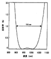
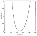
このとき、無反射膜の反射率の波長依存性は、図4に示すように、バスタブ形状に近くなっている。また、無反射膜が1%以下の低反射率で機能する波長の範囲は、177nmになっている。したがって、本実施の形態の無反射膜が1%以下の低反射率で機能する波長の範囲は、従来の無反射膜が1%以下の低反射率で機能する波長の範囲に比較して、非常に広くなっている。 At this time, the wavelength dependence of the reflectance of the antireflection film is close to a bathtub shape as shown in FIG. The range of the wavelength at which the antireflection film functions with a low reflectance of 1% or less is 177 nm. Therefore, the range of wavelengths at which the non-reflective film of the present embodiment functions at a low reflectance of 1% or less is smaller than the range of wavelengths at which the conventional non-reflective film functions at a low reflectance of 1% or less. It is very wide.
後述するように、半導体レーザとファイバグレーティングとを組合わせる場合には、所望の波長λ(たとえば980nm)をバスタブ形状の反射率分布の中心にすることが望ましい。 As described later, when a semiconductor laser and a fiber grating are combined, it is desirable to set a desired wavelength λ (for example, 980 nm) at the center of the bathtub-shaped reflectance distribution.
この場合には、酸化タンタルおよびアルミナの位相φ1および位相φ2をそれぞれ0.488994および0.859283とし、波長λ=940nmで反射率がゼロになるように無反射膜を設計すればよい。 In this case, the phase φ 1 and the phase φ 2 of tantalum oxide and alumina are set to 0.488994 and 0.859283, respectively, and the antireflection film may be designed so that the reflectance becomes zero at the wavelength λ = 940 nm.
なお、このとき各膜の膜厚は、第1の膜/第2の膜/第3の膜/第4の膜/第5の膜/第6の膜/第7の膜=Ad1/Ad2/Bd1/Bd2/Cd1/Cd2/d3=101.36nm/226.16nm/71.13nm/158.71nm/71.13nm/158.71nm/50nmである。 At this time, the thickness of each film is as follows: first film / second film / third film / fourth film / fifth film / sixth film / seventh film = Ad 1 / Ad 2 / Bd 1 / Bd 2 / Cd 1 / Cd 2 / d 3 = 101.36 nm / 226.16 nm / 71.13 nm / 158.71 nm / 71.13 nm / 158.71 nm / 50 nm.
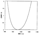
前述の所望の波長λ(たとえば980nm)をバスタブ形状の反射率分布の中心にした無反射膜の反射率の波長依存性を図5に示す。無反射膜が1%以下の低反射率で機能する波長の範囲は166nmである。したがって、この無反射膜が1%以下の低反射率で機能する波長の範囲は、従来の無反射膜が1%以下の低反射率で機能する波長の範囲に比較して、非常に広くなっている。 FIG. 5 shows the wavelength dependence of the reflectance of the non-reflective film with the desired wavelength λ (eg, 980 nm) at the center of the bathtub-shaped reflectance distribution. The range of the wavelength at which the antireflection film functions at a low reflectance of 1% or less is 166 nm. Therefore, the range of wavelengths at which the antireflection film functions at a low reflectance of 1% or less is much wider than the range of wavelengths at which the conventional antireflection film functions at a low reflectance of 1% or less. ing.
実施の形態2.
次に、実施の形態2の半導体光素子装置を図6〜図8を用いて説明する。
Next, a semiconductor optical device according to a second embodiment will be described with reference to FIGS.
本実施の形態の半導体光素子装置は、半導体レーザ31と、屈折率が既知でありかつ膜厚が未知の特定の2種類の膜が3段重ねされた6層構造に、屈折率が既知でありかつ膜厚が既知の特定の1種類の膜が付加された無反射膜とが、屈折率が1である空気または窒素等の空間32内に設けられるように構成されている。
The semiconductor optical device of the present embodiment has a six-layer structure in which a
また、図6に示すように、無反射膜は、酸化タンタル(Ta2O5)の第1の膜14(屈折率n1=2.057、膜厚=Ad1)、アルミナ(Al2O3)の第2の膜15(屈折率n2=1.62、膜厚=Ad2)、酸化タンタル(Ta2O5)の第3の膜16(屈折率n1=2.057、膜厚=Bd1)、アルミナ(Al2O3)の第4の膜17(屈折率n2=1.62、膜厚=Bd2)、酸化タンタル(Ta2O5)の第5の膜18(屈折率n1=2.057、膜厚=Cd1)、アルミナ(Al2O3)の第6の膜19(屈折率n2=1.62、膜厚=Cd2)、および、窒化アルミニウム(AlN)の第7の膜20(屈折率n3=2.072、膜厚d3=50nm)を備えている。なお、膜厚を示す式の中の代数A、BおよびCは、所定のパラメータである。
As shown in FIG. 6, the anti-reflection film is made of a
上記の構成によれば、A=2.7、B=3.0およびC=2.0で、酸化タンタルおよびアルミナの位相φ1および位相φ2がそれぞれ0.671597および0.482534であるとき、波長λ=980nmで、無反射膜の振幅反射率の実部と虚部とをそれぞれゼロにすることができる。 According to the above configuration, when A = 2.7, B = 3.0 and C = 2.0, and the phases φ 1 and φ 2 of tantalum oxide and alumina are 0.671597 and 0.482534, respectively. At the wavelength λ = 980 nm, the real part and the imaginary part of the amplitude reflectance of the antireflection film can be made zero.
また、このとき、各層の膜厚は、第1の膜/第2の膜/第3の膜/第4の膜/第5の膜/第6の膜/第7の膜=Ad1/Ad2/Bd1/Bd2/Cd1/Cd2/d3=137.49nm/125.44nm/152.77nm/139.37nm/101.85nm/92.92nm/50nmである。したがって、トータル膜厚は1489.7nmである。この値は、λ/4に相当する値245nmの約6.1倍である。従来の半導体光素子装置に比較して非常に膜厚が厚いものとなっている。 At this time, the thickness of each layer is as follows: first film / second film / third film / fourth film / fifth film / sixth film / seventh film = Ad 1 / Ad 2 / Bd 1 / Bd 2 / Cd 1 / Cd 2 / d 3 = 137.49 nm / 125.44 nm / 152.77 nm / 139.37 nm / 101.85 nm / 92.92 nm / 50 nm. Therefore, the total film thickness is 1489.7 nm. This value is about 6.1 times the value of 245 nm corresponding to λ / 4. The thickness is much larger than that of the conventional semiconductor optical device.
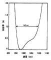
このとき、無反射膜の反射率の波長依存性は、図7に示すように、バスタブ形状に近くなる。また、無反射膜が1%以下の低反射率で機能する波長の範囲は145nmである。したがって、本実施の形態の無反射膜が1%以下の低反射率で機能する波長の範囲は、従来の無反射膜が1%以下の低反射率で機能する波長の範囲に比較して、非常に広くなっている。 At this time, the wavelength dependence of the reflectance of the non-reflective film approaches the shape of a bathtub as shown in FIG. The wavelength range in which the non-reflective film functions at a low reflectance of 1% or less is 145 nm. Therefore, the range of wavelengths at which the non-reflective film of the present embodiment functions at a low reflectance of 1% or less is smaller than the range of wavelengths at which the conventional non-reflective film functions at a low reflectance of 1% or less. It is very wide.
また、所望の波長λ=980nmをバスタブ形状の反射率分布の中心にする場合は、酸化タンタルおよびアルミナの位相φ1および位相φ2をそれぞれ0.685788および0.470145とし、波長λの938nmで反射率をゼロにするように無反射膜を設計すればよい。 When the desired wavelength λ = 980 nm is used as the center of the bathtub-shaped reflectance distribution, the phases φ 1 and φ 2 of tantalum oxide and alumina are set to 0.685788 and 0.470145, respectively, and the wavelength λ of 938 nm is used. What is necessary is just to design a non-reflection film so that a reflectance may be set to zero.
なお、このとき、各膜の膜厚は、第1の膜/第2の膜/第3の膜/第4の膜/第5の膜/第6の膜/第7の膜=Ad1/Ad2/Bd1/Bd2/Cd1/Cd2/d3=134.38nm/116.98nm/149.31nm/129.88nm/99.54nm/86.65/50nmである。
At this time, the thickness of each film is as follows: first film / second film / third film / fourth film / fifth film / sixth film / seventh film = Ad 1 / Ad 2 / Bd 1 / Bd 2 /
前述の無反射膜の反射率の波長依存性を図8に示す。この無反射膜が1%以下の低反射率で機能する波長の範囲は141nmである。したがって、この無反射膜が1%以下の低反射率で機能する波長の範囲は、従来の無反射膜が1%以下の低反射率で機能する波長の範囲に比較して、非常に広くなっている。 FIG. 8 shows the wavelength dependence of the reflectance of the antireflection film. The wavelength range in which this antireflection film functions with a low reflectance of 1% or less is 141 nm. Therefore, the range of wavelengths at which the antireflection film functions at a low reflectance of 1% or less is much wider than the range of wavelengths at which the conventional antireflection film functions at a low reflectance of 1% or less. ing.
実施の形態3.
次に、実施の形態3の半導体光素子装置を図9〜図14を用いて説明する。
Next, a semiconductor optical device according to a third embodiment will be described with reference to FIGS.
図9に示すように、本実施の形態の半導体光素子装置は、半導体レーザ31と、屈折率が既知でありかつ膜厚が未知の特定の2種類の膜が3段重ねされた6層構造に、屈折率が既知でありかつ膜厚が既知の特定の1種類の膜が付加された無反射膜とが、屈折率が1である空気または窒素等の空間32内に設けられている。
As shown in FIG. 9, the semiconductor optical device of the present embodiment has a six-layer structure in which a
また、無反射膜は、窒化アルミニウム(AlN)の第1の膜21(屈折率n3=2.072、膜厚d3=50nm)、酸化タンタル(Ta2O5)の第2の膜22(屈折率n1=2.057、膜厚=Ad1)、アルミナ(Al2O3)の第3の膜23(屈折率n2=1.62、膜厚=Ad2)、酸化タンタル(Ta2O5)の第4の膜24(屈折率n1=2.057、膜厚=Bd1)、アルミナ(Al2O3)の第5の膜25(屈折率n2=1.62、膜厚=Bd2)、酸化タンタル(Ta2O5)の第6の膜26(屈折率n1=2.057、膜厚=Cd1)、および、アルミナ(Al2O3)の第7の膜27(屈折率n2=1.62、膜厚=Cd2)を備えている。また、第1の膜21を構成する窒化アルミニウム(AlN)の膜厚は、50nmである。
The non-reflective film is a
本実施の形態の無反射膜には、窒化アルミニウム、酸化タンタルおよびアルミナの3種類の材料が用いられている。窒化アルミニウムの熱伝導率は、約1.8W/cm/℃である。酸化タンタルの熱伝導率は、約0.1W/cm/℃である。アルミナの熱伝導率は、約0.2W/cm/℃である。したがって、3つの材料のうちで窒化アルミニウムの熱伝導率が最も高い。 For the antireflection film of the present embodiment, three kinds of materials of aluminum nitride, tantalum oxide and alumina are used. Aluminum nitride has a thermal conductivity of about 1.8 W / cm / ° C. The thermal conductivity of tantalum oxide is about 0.1 W / cm / ° C. The thermal conductivity of alumina is about 0.2 W / cm / ° C. Therefore, among the three materials, aluminum nitride has the highest thermal conductivity.
また、A=2.0、B=2.0およびC=2.0で、酸化タンタルおよびアルミナの位相φ1および位相φ2がそれぞれ0.449531および0.991758であるとき、波長λ=980nmで、無反射膜は振幅反射率の実部と虚部とがゼロになる。また、このとき、各層の膜厚は、第1の膜/第2の膜/第3の膜/第4の膜/第5の膜/第6の膜/第7の膜=d3/Ad1/Ad2/Bd1/Bd2/Cd1/Cd2=50nm/68.17nm/190.97nm/68.17nm/190.97nm/68.17nm/190.97nmである。
Further, when A = 2.0, B = 2.0 and C = 2.0 and the phases φ 1 and φ 2 of tantalum oxide and alumina are 0.449531 and 0.991758, respectively, the wavelength λ = 980 nm Thus, the real part and the imaginary part of the amplitude reflectance of the non-reflection film become zero. At this time, the thickness of each layer is as follows: first film / second film / third film / fourth film / fifth film / sixth film / seventh film = d 3 / Ad 1 / a Ad 2 / Bd 1 / Bd 2 /
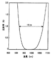
そのため、トータル膜厚は1452.26nmである。トータル膜厚は、波長λの1/4の値である245nmの約5.9倍である。この無反射膜の反射率の波長依存性は、図10に示すようにバスタブ形状に近くなる。また、無反射膜が1%以下の低反射率で機能する波長の範囲は152nmである。 Therefore, the total film thickness is 1452.26 nm. The total film thickness is about 5.9 times the value of 245 nm, which is 4 of the wavelength λ. The wavelength dependence of the reflectance of the non-reflective film is close to a bathtub shape as shown in FIG. The wavelength range in which the non-reflective film functions at a low reflectance of 1% or less is 152 nm.
所望の波長λ=980nmをバスタブ形状の反射率分布の中心にする場合は、酸化タンタルおよびアルミナの位相φ1および位相φ2をそれぞれ0.449325および1.00016とし、波長λ=962nmで、無反射膜の振幅反射率の実部と虚部とをそれぞれゼロにするように無反射膜を設計すればよい。 When the desired wavelength λ = 980 nm is used as the center of the bathtub-shaped reflectance distribution, the phases φ 1 and φ 2 of tantalum oxide and alumina are set to 0.449325 and 1.00016, respectively. The anti-reflection film may be designed so that the real part and the imaginary part of the amplitude reflectance of the reflection film are each set to zero.
なお、このとき、各膜の膜厚は、第1の膜/第2の膜/第3の膜/第4の膜/第5の膜/第6の膜/第7の膜=d3/Ad1/Ad2/Bd1/Bd2/Cd1/Cd2=50nm/55.89nm/189.05nm/66.89nm/189.05nm/66.89nm/189.05nmである。この無反射膜の反射率の波長依存性を図11に示す。この無反射膜が1%以下の低反射率で機能する波長の範囲は151nmとなる。 At this time, the thickness of each film is as follows: first film / second film / third film / fourth film / fifth film / sixth film / seventh film = d 3 / Ad 1 / Ad 2 / Bd 1 / Bd 2 / Cd 1 / Cd 2 = 50 nm / 55.89 nm / 189.05 nm / 66.89 nm / 189.05 nm / 66.89 nm / 189.05 nm. FIG. 11 shows the wavelength dependence of the reflectance of the antireflection film. The range of the wavelength at which this antireflection film functions with a low reflectance of 1% or less is 151 nm.
次に、第1の膜である窒化アルミニウム(AlN)が120nmである無反射膜を図12に示す。 Next, FIG. 12 shows a non-reflection film in which aluminum nitride (AlN) as the first film has a thickness of 120 nm.
図12において、無反射膜は、窒化アルミニウム(AlN)の第1の膜28(屈折率n3=2.072、膜厚d3=120nm)、酸化タンタル(Ta2O5)の第2の膜29(屈折率n1=2.057、膜厚=Ad1)、アルミナ(Al2O3)の第3の膜30(屈折率n2=1.62、膜厚=Ad2)、酸化タンタル(Ta2O5)の第4の膜41(屈折率n1=2.057、膜厚=Bd1)、アルミナ(Al2O3)の第5の膜42(屈折率n2=1.62、膜厚=Bd2)、酸化タンタル(Ta2O5)の第6の膜43(屈折率n1=2.057、膜厚=Cd1)、および、アルミナ(Al2O3)の第7の膜44(屈折率n2=1.62、膜厚=Cd2)を備えている。
In FIG. 12, a non-reflective film is a
また、A=0.9、B=2.0およびC=2.0で、酸化タンタルおよびアルミナの位相φ1および位相φ2がそれぞれ0.726468および0.860316であるとき、波長λ=980nmで、無反射膜は、振幅反射率の実部と虚部とがそれぞれゼロになる。 Further, when A = 0.9, B = 2.0 and C = 2.0, and the phases φ 1 and φ 2 of tantalum oxide and alumina are 0.726468 and 0.860316, respectively, the wavelength λ = 980 nm Thus, in the non-reflection film, the real part and the imaginary part of the amplitude reflectance are each zero.
また、このとき、各層の膜厚は、第1の膜/第2の膜/第3の膜/第4の膜/第5の膜/第6の膜/第7の膜=d3/Ad1/Ad2/Bd1/Bd2/Cd1/Cd2=120nm/49.58nm/74.55nm/110.17nm/165.66nm/110.17nm/165.66nmである。したがって、前述の無反射膜のトータル膜厚は1461.38nmである。すなわち、トータル膜厚は、λ/4である245nmの約6.0倍である。したがって、従来の無反射膜に比較して、トータル膜厚が非常に厚い無反射膜となっている。
At this time, the thickness of each layer is as follows: first film / second film / third film / fourth film / fifth film / sixth film / seventh film = d 3 / Ad 1 / a Ad 2 / Bd 1 / Bd 2 /
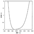
この無反射膜の反射率の波長依存性は、図13に示すように、バスタブ形状に近くなっている。また、無反射膜が1%以下の低反射率で機能する範囲は150nmである。したがって、従来の無反射膜に比較して無反射膜が1%以下の低反射率で機能する範囲が非常に広くなっている。 The wavelength dependence of the reflectance of the antireflection film is close to a bathtub shape as shown in FIG. The range in which the antireflection film functions at a low reflectance of 1% or less is 150 nm. Therefore, the range in which the non-reflective film functions at a low reflectance of 1% or less as compared with the conventional non-reflective film is very wide.
所望の波長λ=980nmをバスタブ形状の反射率分布の中心にする場合には、酸化タンタルおよびアルミナの位相φ1および位相φ2それぞれを0.700522および0.891134とし、波長λ=947nmで無反射膜の反射率をゼロにするように、無反射膜を設計すればよい。 When the desired wavelength λ = 980 nm is used as the center of the bathtub-shaped reflectance distribution, the phases φ 1 and φ 2 of tantalum oxide and alumina are set to 0.700522 and 0.891134, respectively. An anti-reflection film may be designed so that the reflectance of the reflection film becomes zero.
なお、このときの各膜の膜厚は、第1の膜/第2の膜/第3の膜/第4の膜/第5の膜/第6の膜/第7の膜=d3/Ad1/Ad2/Bd1/Bd2/Cd1/Cd2=120nm/46.20nm/74.62nm/102.66nm/165.82nm/102.66nm/165.82nmである。この無反射膜の反射率の波長依存性を図14に示す。無反射膜が1%以下の低反射率で機能する範囲は153nmとなる。
At this time, the thickness of each film is as follows: first film / second film / third film / fourth film / fifth film / sixth film / seventh film = d 3 / Ad 1 / a Ad 2 / Bd 1 / Bd 2 /
なお、本実施の形態の無反射膜では第1膜の窒化アルミニウム膜の膜厚が50nmおよび120nmの場合を示したが、第1膜の窒化アルミニウム膜の膜厚は、この値に限られるものではなく、他の値であっても同様の効果を得ることができる。 In the antireflection film of this embodiment, the case where the thickness of the first aluminum nitride film is 50 nm and 120 nm is shown, but the thickness of the first aluminum nitride film is limited to this value. Instead, the same effect can be obtained with other values.
なお、上記実施の形態1〜3の無反射膜を構成する複数の膜は、それぞれの膜厚と屈折率との積の総和が、半導体光レーザが出射する光の1/4波長よりも大きい場合に、上述の無反射膜の設計手法を用いれば、無反射膜が1%以下の低反射率で機能する波長の範囲を、容易に、従来の無反射膜よりも広くすることができる。 In the plurality of films constituting the antireflection films of the first to third embodiments, the sum of the products of the respective film thicknesses and the refractive indexes is larger than 1 / wavelength of the light emitted by the semiconductor optical laser. In this case, if the above-described method of designing a non-reflective film is used, the range of wavelengths at which the non-reflective film functions at a low reflectance of 1% or less can be easily made wider than the conventional non-reflective film.
また、上述したように、複数の膜のうち半導体光素子に隣接するように設けられた隣接膜は、他の膜よりも熱伝導率が大きいことが望ましい。本実施の形態の半導体素子装置では、隣接膜として、窒化アルミニウムが用いられる例を示したが、これに限定されるものではない。このようにすれば、半導体レーザの熱を効率的に放出することが実現された半導体光素子装置を、上記設計手法を用いて容易に設計することができる。 Further, as described above, it is desirable that, of the plurality of films, the adjacent film provided to be adjacent to the semiconductor optical device has a higher thermal conductivity than the other films. In the semiconductor device of this embodiment, an example in which aluminum nitride is used as the adjacent film has been described, but the present invention is not limited to this. This makes it possible to easily design a semiconductor optical device that can efficiently emit the heat of the semiconductor laser by using the above-described design technique.
また、無反射膜が1%以下の低反射率で機能する波長の範囲は100nm以上であることが望ましい。このようにすれば、通常の状態における半導体光素子が出射する光の波長の変化に柔軟に適応することができる。 Further, the range of the wavelength at which the antireflection film functions at a low reflectance of 1% or less is desirably 100 nm or more. This makes it possible to flexibly adapt to changes in the wavelength of light emitted from the semiconductor optical device in a normal state.
実施の形態4.
次に、本発明の実施の形態の半導体レーザモジュールを、図15〜図18を用いて説明する。図15には、半導体レーザとファイバグレーティングとを備えた半導体レーザモジュールが示されている。
Next, a semiconductor laser module according to an embodiment of the present invention will be described with reference to FIGS. FIG. 15 shows a semiconductor laser module including a semiconductor laser and a fiber grating.
本実施の形態の半導体レーザモジュールは、図15に示すように、半導体レーザ201と、反射率がRfであり、半導体レーザ201の前端面側に設けられた無反射膜203および半導体レーザ201の光導波路領域204からなる半導体素子装置200と、反射率がRrであり、半導体レーザ201の後端面側に設けられた反射膜202と、光導波路領域204から出射した光が通過するレンズ205と、レンズ205が通過した光が導かれる光ファイバ206と、光ファイバ206の光通路に設けられた反射率がRfgであるファイバグレーティング207とを備えている。
As shown in FIG. 15, the semiconductor laser module of the present embodiment has a
本実施の形態の半導体レーザモジュールは、半導体レーザ201の発振波長を安定化させるため、光ファイバ206内にファイバグレーティング207が設けられている。そのため、光ファイバ206内に導かれた特定の波長の光がファイバグレーティング207において反射される。
In the semiconductor laser module of the present embodiment, a fiber grating 207 is provided in an
また、無反射膜203が実施の形態1〜3のうちのいずれかの無反射膜で構成されている。また、反射膜202が無反射膜203よりも高い反射率の膜で構成されている。また、ファイバグレーティング207が、無反射膜203よりも高い反射率の膜で構成されている。それにより、ファイバグレーティング207と反射膜202との間で光が共振するように、ファイバグレーティング207と反射膜202とにより共振器が構成されている。また、レンズ205は、半導体レーザ201から出射した光を効率よく光ファイバ206の光通路内に導くためのものである。
Further, the
図16には、ファイバグレーティング207が設けられた本実施の形態の半導体レーザモジュールの、半導体レーザの利得と損失との関係が示されている。ファイバグレーティング207は、特定の波長λfgに対しては反射率Rfgである。しかしながら、ファイバグレーティング207は、特定の波長λfg以外の波長に対しては反射率はほぼゼロである。このため、図16に示すように、特定の波長λfgで半導体レーザの損失が局所的に極端に小さくなる。図16に示す利得のデータと損失のデータのうち局所的に小さくなっている部分とが交わる。その結果、通常では、特定の波長λfgのとき半導体レーザモジュールは発振する。
FIG. 16 shows the relationship between the gain and the loss of the semiconductor laser in the semiconductor laser module of the present embodiment provided with the
しかしながら、たとえば、周囲温度が低いときは、半導体レーザの利得の分布が波長の小さい側に移動する。そのため、図17に示すように、ファイバグレーティング207で決まる半導体レーザの損失よりも、無反射膜203によって決まる半導体レーザの損失のほうが小さくなる場合がある。このとき、図17に示す利得のデータと損失のデータのうち局所的に小さくなっている部分以外の部分とが交わる。そのため、半導体レーザモジュールは、波長λfgではなく波長λLDで発振する。その結果、波長λfgの光の強度に対する波長λLDの光の強度の比であるサイドモード抑圧比が小さくなってしまうという不都合、または、前述したようなファイバグレーティング207の損失で決まる波長以外の波長で半導体レーザが発振してしまうという不都合が生じる。
However, for example, when the ambient temperature is low, the distribution of the gain of the semiconductor laser moves to the side with the smaller wavelength. Therefore, as shown in FIG. 17, the loss of the semiconductor laser determined by the
本実施の形態の半導体レーザモジュールは、図18に示すように、1%以下の低反射率で機能する範囲が100nm以上である無反射膜203が半導体レーザ201の前端面側に設けられている。そのため、図18に示す損失のデータは、図16および図17の損失のデータのように急峻な反り部を有する曲線ではなく、なだらかな陸り状の曲線になっている。その結果、広い範囲の波長においてファイバグレーティング207で決まる半導体レーザの損失を無反射膜203の反射率で決まる半導体レーザの損失よりも小さくすることができる。すなわち、利得の分布が多少波長が小さい側に移動しようが、多少波長が大きい側に移動しようが、利得のデータと損失のデータのうち局所的に小さくなっている部分とが交わる。したがって、図17に示す波長λLDで発振することを抑制することができるとともに、半導体レーザ201のサイドモード抑圧比が小さくなることを防止することができる。
In the semiconductor laser module of the present embodiment, as shown in FIG. 18, a
なお、上記実施の形態1〜4それぞれの半導体光素子装置としては、無反射膜が7層構造であるものを例にして説明した。しかしながら、本発明の無反射膜の構造は、7層構造に限られるわけではなく、3種類以上の屈折率を有する複数の膜が設けられている構造であれば、9層構造または11層構造等、何層構造であってもよい。 The semiconductor optical device in each of the first to fourth embodiments has been described by taking an example in which the antireflection film has a seven-layer structure. However, the structure of the anti-reflection film of the present invention is not limited to a seven-layer structure, but may be a nine-layer structure or an eleven-layer structure as long as a plurality of films having three or more refractive indexes are provided. Any number of layers may be used.
また、実施の形態1〜4それぞれの無反射膜のパラメータであるA、BおよびCは、各実実施の形態の無反射膜それぞれにおいて一例の所定の数値が示されている。しかしながら、本発明の無反射膜のパラメータは、各実実施の形態の無反射膜に用いた所定の数値に限定されるものではない。無反射膜のパラメータが他の数値であっても、振幅反射率の実部と虚部とをそれぞれゼロにすることができる値でれば、実施の形態1〜4の無反射膜と同様な効果を得ることができる。 A, B, and C, which are the parameters of the antireflection film of each of the first to fourth embodiments, indicate predetermined numerical values as an example in each of the antireflection films of the actual embodiments. However, the parameters of the anti-reflection film of the present invention are not limited to the predetermined numerical values used for the anti-reflection film of each embodiment. Even if the parameter of the anti-reflection film is another numerical value, as long as the real part and the imaginary part of the amplitude reflectivity are values that can be set to zero, the same as the anti-reflection film of the first to fourth embodiments. The effect can be obtained.
なお、実施の形態1〜4それぞれの半導体光素子装置は、無反射膜を構成する複数の膜の屈折率が3種類である場合を例にして説明された。しかしながら、複数の膜のうちの特定の2種類の膜以外の膜の位相条件、すなわち膜厚を予めを設定しておけば、無反射膜を構成する複数の膜の屈折率が4種類以上の場合であっても、特定の2種類の膜を上述の手法、すなわち、複数の膜の振幅反射率の実部と虚部とをゼロにする手法により膜厚が決定された無反射膜であれば、実施の形態1〜4の無反射膜と同様の効果を得ることができる。
In each of the semiconductor optical device devices according to the first to fourth embodiments, the case where the plurality of films constituting the non-reflection film have three types of refractive indexes has been described as an example. However, if the phase conditions of the films other than the specific two types of films among the plurality of films, that is, the film thicknesses are set in advance, the refractive indices of the plurality of films constituting the antireflection film are four or more. Even in this case, the specific two types of films may be non-reflective films whose film thicknesses are determined by the above-described method, that is, a method of setting the real part and the imaginary part of the amplitude reflectance of a plurality of films to zero. If this is the case, the same effects as those of the antireflection films of
さらに、実施の形態1〜3の半導体光素子装置それぞれは、半導体光素子の一例として半導体レーザが用いられている例が示されたが、半導体光素子としては半導体増幅器、スーパールミネッセントダイオードまたは光変調器等の半導体光素子であっても、半導体レーザの場合と同様の効果を得ることができる。 Further, in each of the semiconductor optical device devices according to the first to third embodiments, an example in which the semiconductor laser is used as an example of the semiconductor optical device has been described. However, as the semiconductor optical device, a semiconductor amplifier, a super luminescent diode or Even in the case of a semiconductor optical device such as an optical modulator, the same effect as in the case of a semiconductor laser can be obtained.
また、実施の形態1〜4の半導体光素子装置においては、半導体光素子が出射する光の波長としては、980nm近傍の値を用いたが、半導体光素子が出射する光の波長は、この値に限定されるものではなく、可視光、遠赤外線、および赤外線等であっても、実施の形態1〜4それぞれの半導体光素子装置と同様の効果を得ることができる。 Further, in the semiconductor optical device of the first to fourth embodiments, the wavelength of the light emitted from the semiconductor optical element has a value near 980 nm, but the wavelength of the light emitted by the semiconductor optical element has this value. However, the same effects as those of the semiconductor optical device of each of the first to fourth embodiments can be obtained with visible light, far infrared rays, infrared rays, and the like.
前述のような実施の形態1〜3では、EB(Electron Beam)蒸着法により成膜された膜を用いて半導体光素子装置が構成されていた。しかしながら、EB蒸着法では膜厚の制御性が良好ではない場合がある。したがって、以下の実施の形態5〜7では、ECR(Electron Cyclotron Resonance)スパッタ法を用いることにより膜厚等の制御性が向上した半導体光素子装置が説明される。 In the first to third embodiments as described above, the semiconductor optical element device is configured using the film formed by the EB (Electron Beam) evaporation method. However, there is a case where the controllability of the film thickness is not good in the EB evaporation method. Therefore, in the following fifth to seventh embodiments, a semiconductor optical device in which the controllability such as the film thickness is improved by using an ECR (Electron Cyclotron Resonance) sputtering method will be described.
ただし、ECRスパッタ法を用いる場合には、原因は不明であるが、アルミナ(Al2O3)と酸化タンタル(Ta2O5)との接合性が良好ではない。したがって、実施の形態5〜7では、石英(SiO2)と酸化タンタル(Ta2O5)との接合が利用された半導体光素子装置が用いられる。 However, when the ECR sputtering method is used, although the cause is unknown, the bondability between alumina (Al 2 O 3 ) and tantalum oxide (Ta 2 O 5 ) is not good. Therefore, in the fifth to seventh embodiments, a semiconductor optical device using a junction between quartz (SiO 2 ) and tantalum oxide (Ta 2 O 5 ) is used.
なお、実施の形態5〜7の半導体光素子装置が実施の形態4において説明された半導体レーザに用いられた場合には、実施の形態1〜3の半導体光素子装置が実施の形態4の半導体レーザにより得られる効果と同様の効果を得ることができる。 When the semiconductor optical device of the fifth to seventh embodiments is used for the semiconductor laser described in the fourth embodiment, the semiconductor optical device of the first to third embodiments is replaced with the semiconductor optical device of the fourth embodiment. The same effect as that obtained by the laser can be obtained.
また、以下の実施の形態5〜7のそれぞれにおいては、実施の形態1〜3において説明した2層構造の他に2種類の膜が付加された無反射膜であるが、この無反射膜についても同様に実施の形態1〜3において説明した2層構造の無反射膜の設計手法と同様の手法、すなわち、振幅反射率rの実部と虚部とをそれぞれゼロにする手法を用いることにより、後述する膜厚d1および膜厚d2が算出される。
Further, in each of the following
実施の形態5.
次に、実施の形態5の半導体光素子装置を図21〜図27を用いて説明する。
Next, a semiconductor optical device according to a fifth embodiment will be described with reference to FIGS.
図21に示すように、本実施の形態の半導体光素子装置は、半導体レーザ31と無反射膜とが、屈折率が1である空気または窒素等の空間32内に設けられている。無反射膜は、屈折率が既知でありかつ膜厚が未知の特定の2種類の膜が2段重ねされた4層構造に屈折率が既知でありかつ膜厚が既知の特定の2種類の膜が付加されている。
As shown in FIG. 21, in the semiconductor optical device of the present embodiment, a
より具体的には、無反射膜は、図21に示すように、アルミナ(Al2O3)の第1の膜45(屈折率n3=1.629、膜厚d3)、石英(SiO2)の第2の膜46(屈折率n2=1.484、膜厚=Ad2)、酸化タンタル(Ta2O5)の第3の膜47(屈折率n1=2.072、膜厚=Bd1)、石英(SiO2)の第4の膜48(屈折率n2=1.484、膜厚=Bd2)、酸化タンタル(Ta2O5)の第5の膜49(屈折率n1=2.072、膜厚=Cd1)、および石英(SiO2)の第6の膜50(屈折率n2=1.484、膜厚=Cd2)から構成されている。なお、膜厚を示す式の中の代数A、BおよびCは、上述した実施の形態1〜3と同様に、所定のパラメータである。
More specifically, as shown in FIG. 21, the non-reflective film is a
まず、第1の膜45であるアルミナ(Al2O3)の膜厚d3が10nmの場合の無反射膜が説明される。なお、本実施の形態およびこれ以降の実施の形態においては、ECRスパッタ法による成膜が行われた場合における各層の屈折率の一例が示されている。
First, a description will be given of a non-reflection film when the thickness d 3 of alumina (Al 2 O 3 ) as the
本実施の形態の無反射膜によれば、A=0.18、B=1.99およびC=2.00で、酸化タンタルおよび石英の位相φ1および位相φ2がそれぞれ0.581355および0.899203であるとき、波長λ=980nmで、無反射膜の振幅反射率の実部と虚部とをともにゼロにすることができる。 According to the antireflection film of the present embodiment, A = 0.18, B = 1.99 and C = 2.00, and the phases φ 1 and φ 2 of tantalum oxide and quartz are 0.581355 and 0, respectively. When it is .899203, both the real part and the imaginary part of the amplitude reflectance of the non-reflection film can be made zero at the wavelength λ = 980 nm.
また、このとき、各層の膜厚は、第1の膜/第2の膜/第3の膜/第4の膜/第5の膜/第6の膜=d3/Ad2/Bd1/Bd2/Cd1/Cd2=10/17.01/87.08/188.07/87.52/189.02nmとなる。 At this time, the thickness of each layer is as follows: first film / second film / third film / fourth film / fifth film / sixth film = d 3 / Ad 2 / Bd 1 / the bd 2 / Cd 1 / Cd 2 = 10 / 17.01 / 87.08 / 188.07 / 87.52 / 189.02nm.
したがって、トータル膜厚は962.91nmである。この値は、光の波長λの1/4である膜厚245nmの約3.9倍である。このとき、無反射膜の反射率の波長依存性は、図22に示すようにバスタブ形状に近くなっている。したがって、前述の無反射膜が1%以下の低反射率で機能する波長の範囲は、217nmであり、従来の無反射膜が1%以下の低反射率で機能する波長の範囲に比較して非常に広くなっている。 Therefore, the total film thickness is 962.91 nm. This value is about 3.9 times the film thickness of 245 nm which is 1 / of the wavelength λ of light. At this time, the wavelength dependence of the reflectance of the antireflection film is close to a bathtub shape as shown in FIG. Accordingly, the range of the wavelength at which the above-described non-reflective film functions at a low reflectance of 1% or less is 217 nm, compared with the range of the wavelength at which the conventional non-reflective film functions at a low reflectance of 1% or less. It is very wide.
また、所望の波長λ=980nmをバスタブ形状の反射率分布の中心にする場合は、酸化タンタルおよび石英の位相φ1および位相φ2をそれぞれ0.580136および0.908343とし、波長λ=945nmで反射率をゼロにするように無反射膜を設計すればよい。 When the desired wavelength λ = 980 nm is used as the center of the bathtub-shaped reflectance distribution, the phases φ 1 and φ 2 of tantalum oxide and quartz are set to 0.580136 and 0.908343, respectively. What is necessary is just to design a non-reflection film so that a reflectance may be set to zero.
なお、このときの各膜の膜厚は、第1の膜/第2の膜/第3の膜/第4の膜/第5の膜/第6の膜=d3/Ad2/Bd1/Bd2/Cd1/Cd2=10/16.57/83.80/183.20/84.22/184.12nmである。 At this time, the thickness of each film is as follows: first film / second film / third film / fourth film / fifth film / sixth film = d 3 / Ad 2 / Bd 1 / a Bd 2 / Cd 1 / Cd 2 = 10 / 16.57 / 83.80 / 183.20 / 84.22 / 184.12nm.
前述の無反射膜の反射率の波長依存性を図23に示す。この無反射膜が、1%以下の低反射率で機能する波長の範囲は213nmである。 FIG. 23 shows the wavelength dependence of the reflectance of the antireflection film. The range of the wavelength at which this antireflection film functions with a low reflectance of 1% or less is 213 nm.
次に、第1の膜45であるアルミナ(Al2O3)の膜厚d3が20nmである無反射膜について説明する。前述の無反射膜によれば、A=0.12、B=1.90およびC=2.00で、酸化タンタルおよび石英の位相φ1および位相φ2がそれぞれ0.601513および0.911814であるとき、波長λ=980nmで、反射率がゼロになる。
Next, a description will be given of a non-reflection film in which the thickness d 3 of alumina (Al 2 O 3 ) as the
また、このとき、各層の膜厚は、第1の膜/第2の膜/第3の膜/第4の膜/第5の膜/第6の膜=d3/Ad2/Bd1/Bd2/Cd1/Cd2=20/11.50/86.03/182.08/90.56/191.67nmとなる。トータル膜厚は、970.19nmであり、波長λの1/4の値である245nmの約4.0倍である。 At this time, the thickness of each layer is as follows: first film / second film / third film / fourth film / fifth film / sixth film = d 3 / Ad 2 / Bd 1 / the bd 2 / Cd 1 / Cd 2 = 20 / 11.50 / 86.03 / 182.08 / 90.56 / 191.67nm. The total film thickness is 970.19 nm, which is about 4.0 times the value of 245 nm, which is 1 / of the wavelength λ.
したがって、前述の無反射膜は、従来の無反射膜に比較して、トータル膜厚が非常に厚いものとなっている。このとき、無反射膜の反射率の波長依存性は、図24に示すように、バスタブ形状に近くなっている。また、前述の無反射膜が1%以下の低反射率で機能する範囲は220nmである。したがって、前述の無反射膜は、従来の無反射膜に比較して、無反射膜が1%以下の低反射率で機能する範囲は非常に広くなっている。 Therefore, the above-mentioned non-reflective film has a very large total film thickness as compared with the conventional non-reflective film. At this time, the wavelength dependence of the reflectance of the non-reflective film is close to a bathtub shape as shown in FIG. The range in which the above-described non-reflective film functions at a low reflectance of 1% or less is 220 nm. Therefore, the range in which the above-described non-reflective film functions at a low reflectance of 1% or less is extremely wide as compared with the conventional non-reflective film.
所望の波長λ=980nmをバスタブ形状の反射率分布の中心にする場合は、酸化タンタルおよび石英の位相φ1および位相φ2をそれぞれ0.596734および0.925211とし、波長λ=935nmで無反射膜の反射率をゼロにするように、無反射膜を設計すればよい。 When the desired wavelength λ = 980 nm is used as the center of the reflectance distribution in the bathtub shape, the phases φ 1 and φ 2 of tantalum oxide and quartz are 0.597734 and 0.925211, respectively, and there is no reflection at the wavelength λ = 935 nm. An anti-reflection film may be designed so that the reflectance of the film becomes zero.
なお、このときの各膜の膜厚は、第1の膜/第2の膜/第3の膜/第4の膜/第5の膜/第6の膜=d3/Ad2/Bd1/Bd2/Cd1/Cd2=20/11.13/81.43/176.28/85.71/185.55nmである。前述の無反射膜の反射率の波長依存性を図25に示す。無反射膜が1%以下の低反射率で機能する波長の範囲は215nmとなる。 At this time, the thickness of each film is as follows: first film / second film / third film / fourth film / fifth film / sixth film = d 3 / Ad 2 / Bd 1 / a Bd 2 / Cd 1 / Cd 2 = 20 / 11.13 / 81.43 / 176.28 / 85.71 / 185.55nm. FIG. 25 shows the wavelength dependence of the reflectance of the antireflection film. The wavelength range in which the non-reflective film functions at a low reflectance of 1% or less is 215 nm.
さらに、第1の膜45であるアルミナ(Al2O3)の膜厚d3が40nmである無反射膜について説明する。無反射膜は、A=0.02、B=1.50およびC=2.00で、酸化タンタルおよび石英の位相φ1および位相φ2がそれぞれ0.789974および0.884697であるとき、波長λ=980nmで反射率がゼロになる。
Further, a description will be given of a non-reflection film in which the thickness d 3 of alumina (Al 2 O 3 ) as the
また、このとき、各層の膜厚は、第1の膜/第2の膜/第3の膜/第4の膜/第5の膜/第6の膜=d3/Ad2/Bd1/Bd2/Cd1/Cd2=40/1.86/89.20/139.48/118.93/185.97nmとなる。この無反射膜のトータル膜厚は、982.13nmであり、波長λの1/4である245nmの約4.0倍となる。したがって、このトータル膜厚は、従来の無反射膜のトータル膜厚に比較して非常に厚いものとなっている。 At this time, the thickness of each layer is as follows: first film / second film / third film / fourth film / fifth film / sixth film = d 3 / Ad 2 / Bd 1 / the bd 2 / Cd 1 / Cd 2 = 40 / 1.86 / 89.20 / 139.48 / 118.93 / 185.97nm. The total film thickness of this anti-reflection film is 982.13 nm, which is about 4.0 times 245 nm which is 4 of the wavelength λ. Therefore, this total film thickness is much larger than the total film thickness of the conventional antireflection film.
このときの無反射膜の反射率の波長依存性は、図26に示すように、バスタブ形状に近くなっている。この無反射膜は、1%以下の低反射率で機能する波長の範囲は218nmであり、この範囲は、従来の無反射膜の1%以下の低反射率で機能する波長の範囲に比較して非常に広い。 At this time, the wavelength dependence of the reflectance of the antireflection film is close to a bathtub shape as shown in FIG. This antireflection film has a wavelength range of 218 nm that functions at a low reflectance of 1% or less, which is smaller than that of a conventional antireflection film at a low reflectance of 1% or less. And very wide.
所望の波長λ=980nmをバスタブ形状の反射率分布の中心にする場合は、酸化タンタルおよび石英の位相φ1および位相φ2をそれぞれ0.774569および0.901877とし、波長λ=927nmで無反射膜の反射率をゼロにするように無反射膜を設計する。 When the desired wavelength λ = 980 nm is used as the center of the bathtub-shaped reflectance distribution, the phases φ 1 and φ 2 of tantalum oxide and quartz are set to 0.774569 and 0.901877, respectively, and there is no reflection at the wavelength λ = 927 nm. A non-reflective film is designed so that the reflectance of the film becomes zero.
なお、このときの各膜の膜厚は、第1の膜/第2の膜/第3の膜/第4の膜/第5の膜/第6の膜=d3/Ad2/Bd1/Bd2/Cd1/Cd2=40/1.79/82.73/134.50/110.31/179.33nmである。無反射膜の反射率の波長依存性を図27に示す。無反射膜は、1%以下の低反射率で機能する波長の範囲が208nmとなる。 At this time, the thickness of each film is as follows: first film / second film / third film / fourth film / fifth film / sixth film = d 3 / Ad 2 / Bd 1 / a Bd 2 / Cd 1 / Cd 2 = 40 / 1.79 / 82.73 / 134.50 / 110.31 / 179.33nm. FIG. 27 shows the wavelength dependence of the reflectance of the non-reflective film. The non-reflective film has a wavelength range of 208 nm that functions with a low reflectance of 1% or less.
なお、前述の6層構造の無反射膜の設計手法では、次に示す式(8)が用いられる。この式(8)を用いた場合にも、式(3c)で示す振幅反射率rの実部と虚部とがそれぞれゼロになるように、膜厚d1および膜厚d2が算出される。 In the above-described method for designing a six-layer antireflection film, the following equation (8) is used. Also when this equation (8) is used, the film thickness d 1 and the film thickness d 2 are calculated such that the real part and the imaginary part of the amplitude reflectance r shown in the equation (3c) are each zero. .
実施の形態6.
次に、実施の形態6の半導体光素子装置を図28〜図34を用いて説明する。
Embodiment 6 FIG.
Next, a semiconductor optical device according to the sixth embodiment will be described with reference to FIGS.
図28に示すように、本実施の形態の半導体光素子装置は、半導体レーザ31と無反射膜とが、屈折率が1である空気または窒素等の空間32内に設けられている。無反射膜は、屈折率が既知でありかつ膜厚が未知の特定の2種類の膜が3段重ねされた6層構造に屈折率が既知でありかつ膜厚が既知の特定の2種類の膜が付加されている。
As shown in FIG. 28, in the semiconductor optical device of this embodiment, a
図28に示すように、本実施の形態の無反射膜は、アルミナ(Al2O3)の第1の膜51(屈折率n3=1.629、膜厚d3)、石英(SiO2)の第2の膜52(屈折率n2=1.484、膜厚=Ad2)、酸化タンタル(Ta2O5)の第3の膜53(屈折率n1=2.072、膜厚=Bd1)、石英(SiO2)の第4の膜54(屈折率n2=1.484、膜厚=Bd2)、酸化タンタル(Ta2O5)の第5の膜55(屈折率n1=2.072、膜厚=Cd1)、石英(SiO2)の第6の膜56(屈折率n2=1.484、膜厚=Cd2)、酸化タンタル(Ta2O5)の第7の膜57(屈折率n1=2.072、膜厚=Dd1)、および石英(SiO2)の第8の膜58(屈折率n2=1.484、膜厚=Dd2)により構成されている。
As shown in FIG. 28, the antireflection film of the present embodiment is made of a
まず、第1の膜51であるアルミナ(Al2O3)の膜厚d3が10nmである無反射膜について説明する。
First, a description will be given of a non-reflective film having a thickness d 3 of 10 nm of alumina (Al 2 O 3 ) which is the
前述の無反射膜は、A=0.50、B=2.00、C=2.00およびD=2.00で、酸化タンタルおよび石英の位相φ1および位相φ2がそれぞれ0.356965および1.03993であるとき、波長λ=980nmで反射率をゼロにすることができる。 In the antireflection film described above, A = 0.50, B = 2.00, C = 2.00 and D = 2.00, and the phases φ 1 and φ 2 of tantalum oxide and quartz were 0.356965 and 0.356965, respectively. When it is 1.03993, the reflectance can be made zero at the wavelength λ = 980 nm.
また、このとき、各層の膜厚は、第1の膜/第2の膜/第3の膜/第4の膜/第5の膜/第6の膜/第7の膜/第8の膜=d3/Ad2/Bd1/Bd2/Cd1/Cd2/Dd1/Dd2=10/54.65/53.74/218.60/53.74/218.60/53.74/218.60nmとなる。この無反射膜のトータル膜厚は、1404.65nmであり、波長λの1/4である245nmの約5.7倍である。 At this time, the thickness of each layer is as follows: first film / second film / third film / fourth film / fifth film / sixth film / seventh film / eighth film. = D 3 / Ad 2 / Bd 1 / Bd 2 / Cd 1 / Cd 2 / Dd 1 / Dd 2 = 10 / 54.65 / 53.74 / 218.60 / 53.74 / 218.60 / 53.74 /218.60 nm. The total film thickness of this anti-reflection film is 1404.65 nm, which is about 5.7 times 245 nm which is 4 of the wavelength λ.
したがって、このトータル膜厚は、従来の無反射膜のトータル膜厚に比較して非常に厚い。このとき、無反射膜の反射率の波長依存性は、図29に示すように、バスタブ形状に近くなっている。また、無反射膜は、1%以下の低反射率で機能する波長の範囲が116nmであり、その範囲は従来の無反射膜の1%以下の低反射率で機能する波長の範囲と比較して非常に広いものである。 Therefore, this total film thickness is much larger than the total film thickness of the conventional antireflection film. At this time, the wavelength dependence of the reflectance of the non-reflective film is close to a bathtub shape as shown in FIG. The wavelength range of the non-reflective film that functions at a low reflectance of 1% or less is 116 nm, which is smaller than that of the conventional non-reflective film that functions at a low reflectance of 1% or less. And very wide.
所望の波長λ=980nmをバスタブ形状の反射率分布の中心にする場合は、酸化タンタルおよび石英の位相φ1および位相φ1をそれぞれ0.357013および1.0386とし、波長λ=971nmで無反射膜の反射率をゼロにすればよい。 If the desired wavelength lambda = 980 nm in the center of the reflectance distribution of the bathtub-shaped, tantalum oxide and quartz phase phi 1 and the phase phi 1 respectively and 0.357013 and 1.0386, nonreflective at the wavelength λ = 971nm What is necessary is just to make the reflectance of the film zero.
なお、このときの各膜の膜厚は、第1の膜/第2の膜/第3の膜/第4の膜/第5の膜/第6の膜/第7の膜/第8の膜=d3/Ad2/Bd1/Bd2/Cd1/Cd2/Dd1/Dd2=10/54.08/53.26/216.31/53.26/216.31/53.26/216.31nmである。前述の無反射膜の反射率の波長依存性を図30に示す。この無反射膜は、1%以下の低反射率で機能する波長の範囲が115nmである。 Note that the thickness of each film at this time is as follows: first film / second film / third film / fourth film / fifth film / sixth film / seventh film / eighth film. Film = d 3 / Ad 2 / Bd 1 / Bd 2 / Cd 1 / Cd 2 / Dd 1 / Dd 2 = 10 / 54.08 / 53.26 / 216.31 / 53.26 / 216.31 / 53. 26 / 216.31 nm. FIG. 30 shows the wavelength dependence of the reflectance of the anti-reflection film. This antireflection film has a wavelength range of 115 nm that functions with a low reflectance of 1% or less.
次に、第1の膜51であるアルミナ(Al2O3)の膜厚d3が20nmである無反射膜について説明する。無反射膜は、A=0.42、B=2.00、C=2.00およびD=2.00で、酸化タンタルおよび石英の位相φ1および位相φ2がそれぞれ0.355425および1.03088であるとき、波長λ=980nmで反射率がゼロになる。
Next, a description will be given of a non-reflection film in which the thickness d 3 of alumina (Al 2 O 3 ) as the
また、このときの各層の膜厚は、第1の膜/第2の膜/第3の膜/第4の膜/第5の膜/第6の膜/第7の膜/第8の膜=d3/Ad2/Bd1/Bd2/Cd1/Cd2/Dd1/Dd2=20/45.51/53.51/216.70/53.51/216.70/53.51/216.70nmとなる。トータル膜厚は、1397.48nmであり、波長λの1/4である245nmの約5.7倍である。 At this time, the thickness of each layer is as follows: first film / second film / third film / fourth film / fifth film / sixth film / seventh film / eighth film. = D 3 / Ad 2 / Bd 1 / Bd 2 / Cd 1 / Cd 2 / Dd 1 / Dd 2 = 20 / 44.51 / 53.51 / 216.70 / 53.51 / 216.70 / 53.51 /216.70 nm. The total film thickness is 1397.48 nm, which is about 5.7 times 245 nm which is の of the wavelength λ.
したがって、このトータル膜厚は、従来の無反射膜のトータル膜厚に比較してと非常に大きい値である。このときの無反射膜の反射率の波長依存性は、図31に示すように、バスタブ形状に近くなっている。この無反射膜は、1%以下の低反射率で機能する波長の範囲が116nmであり、この値は、従来の無反射膜の1%以下の低反射率で機能する波長の範囲に比較して非常に大きい値である。 Therefore, this total film thickness is an extremely large value as compared with the total film thickness of the conventional antireflection film. At this time, the wavelength dependence of the reflectance of the antireflection film is close to a bathtub shape as shown in FIG. This non-reflective film has a wavelength range of 116 nm that functions at a low reflectance of 1% or less, which is smaller than the wavelength range of a conventional non-reflective film that functions at a low reflectance of 1% or less. It is a very large value.
所望の波長λ=98nmをバスタブ形状の反射率分布の中心にする場合は、酸化タンタルおよび石英の位相φ1および位相φ2をそれぞれ0.35537および1.02959とし、波長λ=975nmで無反射膜の反射率をゼロにするように無反射膜を設計する。 When the desired wavelength λ = 98 nm is used as the center of the bathtub-shaped reflectance distribution, the phases φ 1 and φ 2 of tantalum oxide and quartz are 0.35537 and 1.02959, respectively, and there is no reflection at the wavelength λ = 975 nm. A non-reflective film is designed so that the reflectance of the film becomes zero.
なお、このときの各膜の膜厚は、第1の膜/第2の膜/第3の膜/第4の膜/第5の膜/第6の膜/第7の膜/第8の膜=d3/Ad2/Bd1/Bd2/Cd1/Cd2/Dd1/Dd2=20/45.22/53.23/215.32/53.23/215.32/53.23/215.32nmである。前述の無反射膜の反射率の波長依存性を図32に示す。この無反射膜は、1%以下の低反射率で機能する波長の範囲が115nmである。 Note that the thickness of each film at this time is as follows: first film / second film / third film / fourth film / fifth film / sixth film / seventh film / eighth film. Film = d 3 / Ad 2 / Bd 1 / Bd 2 / Cd 1 / Cd 2 / Dd 1 / Dd 2 = 20 / 45.22 / 53.23 / 215.32 / 53.23 / 215.32 / 53. 23 / 215.32 nm. FIG. 32 shows the wavelength dependence of the reflectance of the antireflection film. This antireflection film has a wavelength range of 115 nm that functions with a low reflectance of 1% or less.
さらに、第1の膜51であるアルミナ(Al2O3)の膜厚d3が40nmである無反射膜について説明する。無反射膜は、A=0.30、B=1.95、C=2.00およびD=2.00であり、酸化タンタルおよび石英の位相φ1および位相φ2がそれぞれ0.356112および1.00038であるとき、波長λ=980nmで反射率がゼロになる。
Further, a description will be given of a non-reflection film in which the thickness d 3 of alumina (Al 2 O 3 ) as the
また、このとき、各層の膜厚は、第1の膜/第2の膜/第3の膜/第4の膜/第5の膜/第6の膜/第7の膜/第8の膜=d3/Ad2/Bd1/Bd2/Cd1/Cd2/Dd1/Dd2=40/31.54/52.27/205.03/53.61/210.28/53.61/210.28nmとなる。トータル膜厚は、1370.80nmであり、波長λの1/4である245nmの約5.6倍になる。 At this time, the thickness of each layer is as follows: first film / second film / third film / fourth film / fifth film / sixth film / seventh film / eighth film. = D 3 / Ad 2 / Bd 1 / Bd 2 / Cd 1 / Cd 2 / Dd 1 / Dd 2 = 40 / 31.54 / 52.27 / 205.03 / 53.61 / 210.28 / 53.61 /210.28 nm. The total film thickness is 1370.80 nm, which is about 5.6 times 245 nm which is 1 / of the wavelength λ.
したがって、このトータル膜厚は、従来の無反射膜のトータル膜厚に比較して非常に厚い。このとき無反射膜の反射率の波長依存性は、図33に示すように、バスタブ形状に近くなっている。この無反射膜は、1%以下の低反射率で機能する波長の範囲が110nmであり、その範囲は従来の無反射膜の1%以下の低反射率で機能する波長の範囲に比較して非常に広い。 Therefore, this total film thickness is much larger than the total film thickness of the conventional antireflection film. At this time, the wavelength dependence of the reflectance of the non-reflective film is close to a bathtub shape as shown in FIG. This non-reflective film has a wavelength range of 110 nm which functions at a low reflectance of 1% or less, which is smaller than that of a conventional non-reflective film at a low reflectance of 1% or less. Very wide.
所望の波長λ=980nmをバスタブ形状の反射率分布の中心にする場合は、酸化タンタルおよび石英の位相φ1および位相φ2をそれぞれ0.356344および1.0013とし、波長λ=983nmで、無反射膜の反射率をゼロにするように無反射膜を設計する。 When the desired wavelength λ = 980 nm is set as the center of the bathtub-shaped reflectance distribution, the phases φ 1 and φ 2 of tantalum oxide and quartz are 0.356344 and 1.0013, respectively. The non-reflective film is designed so that the reflectivity of the reflective film becomes zero.
なお、このときの各膜の膜厚は、第1の膜/第2の膜/第3の膜/第4の膜/第5の膜/第6の膜/第7の膜/第8の膜=d3/Ad2/Bd1/Bd2/Cd1/Cd2/Dd1/Dd2=40/31.67/52.47/205.85/53.81/211.12/53.81/211.12nmである。無反射膜の反射率の波長依存性を図34に示す。無反射膜は、1%以下の低反射率で機能する波長の範囲が111nmである。 Note that the thickness of each film at this time is as follows: first film / second film / third film / fourth film / fifth film / sixth film / seventh film / eighth film. Film = d 3 / Ad 2 / Bd 1 / Bd 2 / Cd 1 / Cd 2 / Dd 1 / Dd 2 = 40 / 31.67 / 52.47 / 205.85 / 53.81 / 211.12 / 53. 81 / 211.12 nm. FIG. 34 shows the wavelength dependence of the reflectance of the non-reflective film. The non-reflective film has a wavelength range of 111 nm that functions at a low reflectance of 1% or less.
また、前述の8層構造の無反射膜の設計手法では、次に示す式(9)が用いられる。この式(9)を用いた場合にも、式(3c)で示す振幅反射率rの実部と虚部とがそれぞれゼロになるように、膜厚d1および膜厚d2が算出される。 Further, in the design method of the antireflection film having the eight-layer structure described above, the following equation (9) is used. Also when this equation (9) is used, the film thickness d 1 and the film thickness d 2 are calculated such that the real part and the imaginary part of the amplitude reflectance r shown in the equation (3c) are each zero. .
実施の形態7.
次に、実施の形態7の半導体光素子装置を図35〜図41を用いて説明する。
Next, a semiconductor optical device according to a seventh embodiment will be described with reference to FIGS.
図35に示すように、本実施の形態の半導体光素子装置は、半導体レーザ31と無反射膜とが、屈折率が1である空気または窒素等の空間32内に設けられている。無反射膜は、屈折率が既知でありかつ膜厚が未知の特定の2種類の膜が4段重ねされた8層構造に屈折率が既知でありかつ膜厚が既知の特定の2種類の膜が付加されている。
As shown in FIG. 35, in the semiconductor optical device of the present embodiment, a
図35に示すように、アルミナ(Al2O3)の第1の膜59(屈折率n3=1.629、膜厚d3)、石英(SiO2)の第2の膜60(屈折率n2=1.484、膜厚=Ad2)、酸化タンタル(Ta2O5)の第3の膜61(屈折率n1=2.072、膜厚=Bd1)、石英(SiO2)の第4の膜62(屈折率n2=1.484、膜厚=Bd2)、酸化タンタル(Ta2O5)の第5の膜63(屈折率n1=2.072、膜厚=Cd1)、石英(SiO2)の第6の膜64(屈折率n2=1.484、膜厚=Cd2)、酸化タンタル(Ta2O5)の第7の膜65(屈折率n1=2.072、膜厚=Dd1)、石英(SiO2)の第8の膜66(屈折率n2=1.484、膜厚=Dd2)、酸化タンタル(Ta2O5)の第9の膜67(屈折率n1=2.072、膜厚=Ed1)、および石英(SiO2)の第10の膜68(屈折率n2=1.484、膜厚=Ed2)から構成されている。
As shown in FIG. 35, a
まず、第1の膜59であるアルミナ(Al2O3)の膜厚d3が10nmである無反射膜について説明する。
First, a description will be given of a non-reflection film in which the thickness d 3 of alumina (Al 2 O 3 ) is 10 nm, which is the
前述の無反射膜は、A=0.62、B=2.00、C=2.00、D=2.00およびE=2.00で、酸化タンタルおよび石英の位相φ1および位相φ2がそれぞれ0.276571および1.1374であるとき、波長λ=980nmで反射率がゼロになる。 The antireflection film described above has A = 0.62, B = 2.00, C = 2.00, D = 2.00 and E = 2.00, and has a phase φ 1 and a phase φ 2 of tantalum oxide and quartz. Are 0.276571 and 1.1374, respectively, the reflectance becomes zero at the wavelength λ = 980 nm.
また、このとき、各層の膜厚は、第1の膜/第2の膜/第3の膜/第4の膜/第5の膜/第6の膜/第7の膜/第8の膜/第9の膜/第10の膜=d3/Ad2/Bd1/Bd2/Cd1/Cd2/Dd1/Dd2/Ed1/Ed2=10/74.12/41.64/239.09/41.64/239.09/51.64/239.09/41.64/239.09nmとなる。トータル膜厚は、1890.63nmであり、波長λの1/4である245nmの約7.7倍である。したがって、このトータル膜厚は、従来の無反射膜のトータル膜厚に比較して非常に大きな値となっている。
At this time, the thickness of each layer is as follows: first film / second film / third film / fourth film / fifth film / sixth film / seventh film / eighth film. / ninth film / 10th of
このときの無反射膜の反射率の波長依存性は、図36に示すように、バスタブ形状に近くなっている。この無反射膜は、1%以下の低反射率で機能する波長の範囲が79nmであり、その値は従来の無反射膜の1%以下の低反射率で機能する波長の範囲に比較して大きな値となっている。 At this time, the wavelength dependence of the reflectance of the antireflection film is close to a bathtub shape as shown in FIG. This non-reflective film has a wavelength range of 79 nm that functions at a low reflectance of 1% or less, which is compared with the wavelength range of a conventional non-reflective film that functions at a low reflectance of 1% or less. It has a large value.
所望の波長λ=980nmをバスタブ形状の反射率分布の中心にする場合は、酸化タンタルおよび石英の位相φ1および位相φ2をそれぞれ0.276804および1.13636とし、波長λ=971nmで無反射膜の反射率をゼロにするように無反射膜を設計する。 When the desired wavelength λ = 980 nm is used as the center of the bathtub-shaped reflectance distribution, the phases φ 1 and φ 2 of tantalum oxide and quartz are 0.276804 and 1.13636, respectively, and there is no reflection at the wavelength λ = 971 nm. A non-reflective film is designed so that the reflectance of the film becomes zero.
なお、このときの各膜の膜厚は、第1の膜/第2の膜/第3の膜/第4の膜/第5の膜/第6の膜/第7の膜/第8の膜/第9の膜/第10の膜=d3/Ad2/Bd1/Bd2/Cd1/Cd2/Dd1/Dd2/Ed1/Ed2=10/73.37/41.29/236.67/41.29/236.67/41.29/236.67/41.29/236.67nmである。無反射膜の反射率の波長依存性を図37に示す。この無反射膜は、1%以下の低反射率で機能する波長の範囲が77nmである。 Note that the thickness of each film at this time is as follows: first film / second film / third film / fourth film / fifth film / sixth film / seventh film / eighth film. Film / ninth film / tenth film = d 3 / Ad 2 / Bd 1 / Bd 2 / Cd 1 / Cd 2 / Dd 1 / Dd 2 / Ed 1 / Ed 2 = 10 / 73.37 / 41. 29 / 236.67 / 41.29 / 236.67 / 41.29 / 236.67 / 41.29 / 236.67 nm. FIG. 37 shows the wavelength dependence of the reflectance of the non-reflective film. This antireflection film has a wavelength range of 77 nm that functions with a low reflectance of 1% or less.
次に、第1の膜59であるアルミナ(Al2O3)の膜厚d3が20nmである無反射膜について説明する。前述の無反射膜は、A=0.54、B=2.00、C=2.00、D=2.00およびE=2.00で、酸化タンタルおよび石英の位相φ1および位相φ2がそれぞれ0.2754045および1.1399であるとき、波長λ=980nmで反射率がゼロになる。
Next, a description will be given of a non-reflection film in which the thickness d 3 of alumina (Al 2 O 3 ) is 20 nm, which is the
また、このとき、各層の膜厚は、第1の膜/第2の膜/第3の膜/第4の膜/第5の膜/第6の膜/第7の膜/第8の膜/第9の膜/第10の膜=d3/Ad2/Bd1/Bd2/Cd1/Cd2/Dd1/Dd2/Ed1/Ed2=20/64.70/41.41/239.61/41.41/239.61/41.41/239.61/41.41/239.61nmとなる。トータル膜厚は、1894.13nmであり、波長λの1/4である245nmの約7.7倍になる。したがって、このトータル膜厚は、従来の無反射膜のトータル膜厚に比較して非常に大きい値になっている。 At this time, the thickness of each layer is as follows: first film / second film / third film / fourth film / fifth film / sixth film / seventh film / eighth film. / Ninth film / tenth film = d 3 / Ad 2 / Bd 1 / Bd 2 / Cd 1 / Cd 2 / Dd 1 / Dd 2 / Ed 1 / Ed 2 = 20 / 64.70 / 41.41 /239.61/41.41/239.61/41.41.4/239.61/41.41/239.61 nm. The total film thickness is 1894.13 nm, which is about 7.7 times 245 nm which is 4 of the wavelength λ. Therefore, this total film thickness is a very large value compared to the total film thickness of the conventional anti-reflection film.
このときの無反射膜の反射率の波長依存性は、図38に示すように、バスタブ形状に近くなる。この無反射膜は、1%以下の低反射率で機能する波長の範囲が80nmであり、この値は従来の無反射膜の1%以下の低反射率で機能する波長の範囲に比較して大きな値である。 At this time, the wavelength dependence of the reflectance of the non-reflective film approaches the shape of a bathtub as shown in FIG. This antireflection film has a wavelength range of 80 nm that functions at a low reflectance of 1% or less, which is smaller than that of a conventional antireflection film at a low reflectance of 1% or less. This is a large value.
所望の波長λ=980nmをバスタブ形状の反射率分布の中心にする場合は、酸化タンタルおよび石英の位相φ1および位相φ2をそれぞれ0.275567および1.13754とし、波長λ=971nmで、無反射膜の反射率をゼロにするように無反射膜を設計する。 When the desired wavelength λ = 980 nm is used as the center of the bathtub-shaped reflectance distribution, the phases φ 1 and φ 2 of tantalum oxide and quartz are 0.275567 and 1.13754, respectively. The non-reflective film is designed so that the reflectivity of the reflective film becomes zero.
なお、このときの各膜の膜厚は、第1の膜/第2の膜/第3の膜/第4の膜/第5の膜/第6の膜/第7の膜/第8の膜/第9の膜/第10の膜=d3/Ad2/Bd1/Bd2/Cd1/Cd2/Dd1/Dd2/Ed1/Ed2=20/63.97/41.11/236.92/41.11/236.92/41.11/236.92/41.11/236.92nmである。この無反射膜の反射率の波長依存性を図39に示す。この無反射膜は、1%以下の低反射率で機能する波長の範囲が79nmである。 Note that the thickness of each film at this time is as follows: first film / second film / third film / fourth film / fifth film / sixth film / seventh film / eighth film. Film / ninth film / tenth film = d 3 / Ad 2 / Bd 1 / Bd 2 / Cd 1 / Cd 2 / Dd 1 / Dd 2 / Ed 1 / Ed 2 = 20 / 63.97 / 41. 11 / 236.92 / 41.11 / 236.92 / 41.11 / 236.92 / 41.11 / 236.92 nm. FIG. 39 shows the wavelength dependence of the reflectance of the antireflection film. This antireflection film has a wavelength range of 79 nm which functions at a low reflectance of 1% or less.
次に、第1の膜59であるアルミナ(Al2O3)の膜厚d3が40nmである無反射膜について説明する。前述の無反射膜は、A=0.40、B=2.00、C=2.00、D=2.00およびE=2.00で、酸化タンタルおよび石英の位相φ1および位相φ2がそれぞれ0.275565および1.11479であるとき、波長λ=980nmで反射率がゼロになる。
Next, a description will be given of a non-reflection film in which the thickness d 3 of alumina (Al 2 O 3 ) is 40 nm, which is the
また、このとき、各層の膜厚は、第1の膜/第2の膜/第3の膜/第4の膜/第5の膜/第6の膜/第7の膜/第8の膜/第9の膜/第10の膜=d3/Ad2/Bd1/Bd2/Cd1/Cd2/Dd1/Dd2/Ed1/Ed2=40/46.87/41.49/234.34/41.49/234.34/41.49/234.34/41.49/234.34nmとなる。トータル膜厚は、1869.63nmであり、波長λの1/4である245nmの約7.6倍になる。したがって、このトータル膜厚は、従来の無反射膜のトータル膜厚に比較して非常に大きい値になっている。 At this time, the thickness of each layer is as follows: first film / second film / third film / fourth film / fifth film / sixth film / seventh film / eighth film. / Ninth film / tenth film = d 3 / Ad 2 / Bd 1 / Bd 2 / Cd 1 / Cd 2 / Dd 1 / Dd 2 / Ed 1 / Ed 2 = 40 / 46.87 / 41.49 /234.34/41.49/234.34/41.49/234.34/41.49/234.34 nm. The total film thickness is 186.63 nm, which is about 7.6 times 245 nm which is 1 / of the wavelength λ. Therefore, this total film thickness is a very large value compared to the total film thickness of the conventional anti-reflection film.
このときの無反射膜の反射率の波長依存性は、図40に示すように、バスタブ形状に近くなる。この無反射膜は、1%以下の低反射率で機能する波長の範囲が79nmであり、この値は従来の無反射膜の1%以下の低反射率で機能する波長の範囲に比較して大きな値である。 At this time, the wavelength dependence of the reflectance of the non-reflective film approaches the shape of a bathtub as shown in FIG. This non-reflective film has a wavelength range of 79 nm that functions at a low reflectance of 1% or less, which is smaller than that of a conventional non-reflective film at a low reflectance of 1% or less. This is a large value.
所望の波長λ=980nmをバスタブ形状の反射率分布の中心にする場合は、酸化タンタルおよび石英の位相φ1および位相φ2をそれぞれ0.275663および1.11367とし、波長λ=977nmで、無反射膜の反射率をゼロにするように無反射膜を設計する。 When the desired wavelength λ = 980 nm is used as the center of the bathtub-shaped reflectance distribution, the phases φ 1 and φ 2 of tantalum oxide and quartz are 0.275663 and 1.11367, respectively. The non-reflective film is designed so that the reflectivity of the reflective film becomes zero.
なお、このときの各膜の膜厚は、第1の膜/第2の膜/第3の膜/第4の膜/第5の膜/第6の膜/第7の膜/第8の膜/第9の膜/第10の膜=d3/Ad2/Bd1/Bd2/Cd1/Cd2/Dd1/Dd2/Ed1/Ed2=40/46.68/41.37/233.38/41.37/233.38/41.37/233.38/41.37/233.38nmである。この無反射膜の反射率の波長依存性を図41に示す。この無反射膜は、1%以下の低反射率で機能する波長の範囲が78nmである。 Note that the thickness of each film at this time is as follows: first film / second film / third film / fourth film / fifth film / sixth film / seventh film / eighth film. Film / ninth film / tenth film = d 3 / Ad 2 / Bd 1 / Bd 2 / Cd 1 / Cd 2 / Dd 1 / Dd 2 / Ed 1 / Ed 2 = 40 / 46.68 / 41. 37 / 233.38 / 41.37 / 233.38 / 41.37 / 233.38 / 41.37 / 233.38 nm. FIG. 41 shows the wavelength dependence of the reflectance of the antireflection film. This antireflection film has a wavelength range of 78 nm that functions with a low reflectance of 1% or less.
また、前述の10層構造の無反射膜の設計手法では、次に示す式(10)が用いられる。この式(10)を用いた場合にも、式(3c)で示す振幅反射率rの実部と虚部とがそれぞれゼロになるように、膜厚d1および膜厚d2が算出される。 In the above-described design method of the antireflection film having the ten-layer structure, the following equation (10) is used. Also when this equation (10) is used, the film thickness d 1 and the film thickness d 2 are calculated such that the real part and the imaginary part of the amplitude reflectance r shown in the equation (3c) are each zero. .
また、実施の形態5〜7それぞれの無反射膜のパラメータであるA、B、C、DおよびEは、各実実施の形態の無反射膜それぞれにおいて一例の所定の数値が示されている。しかしながら、本発明の無反射膜のパラメータは、各実実施の形態の無反射膜に用いた所定の数値に限定されるものではない。無反射膜のパラメータが他の数値であっても、振幅反射率の実部と虚部とをそれぞれゼロにすることができる値でれば、実施の形態5〜7の無反射膜と同様な効果を得ることができる。 A, B, C, D, and E, which are the parameters of the antireflection film of each of the fifth to seventh embodiments, indicate predetermined examples of the antireflection film of each actual embodiment. However, the parameters of the anti-reflection film of the present invention are not limited to the predetermined numerical values used for the anti-reflection film of each embodiment. Even if the parameter of the anti-reflection film is another numerical value, as long as the real part and the imaginary part of the amplitude reflectance can be set to zero, the same as the anti-reflection film of the fifth to seventh embodiments is obtained. The effect can be obtained.
また、実施の形態5〜7それぞれの半導体光素子装置は、無反射膜を構成する複数の膜の屈折率が3種類である場合を例にして説明された。しかしながら、複数の膜のうちの特定の2種類の膜以外の膜の位相条件、すなわち膜厚を予めを設定しておけば、無反射膜を構成する複数の膜の屈折率が4種類以上の場合であっても、特定の2種類の膜を上述の手法、すなわち、複数の膜の振幅反射率の実部と虚部とをゼロにする手法により膜厚が決定された無反射膜であれば、実施の形態5〜7の無反射膜と同様の効果を得ることができる。 Further, each of the semiconductor optical device devices according to the fifth to seventh embodiments has been described by taking, as an example, a case where a plurality of films constituting the anti-reflection film have three types of refractive indexes. However, if the phase conditions of the films other than the specific two types of films among the plurality of films, that is, the film thicknesses are set in advance, the refractive indices of the plurality of films constituting the antireflection film are four or more. Even in this case, the specific two types of films may be non-reflective films whose film thicknesses are determined by the above-described method, that is, a method of setting the real part and the imaginary part of the amplitude reflectance of a plurality of films to zero. In this case, the same effects as those of the antireflection films of the fifth to seventh embodiments can be obtained.
また、実施の形態5〜7においては、第1の膜のアルミナの膜厚が10nm、20nmおよび40nmの場合の無反射膜を示したが、アルミナの膜厚はこれら値に限定されるものではない。
Further, in
また、実施の形態5〜7においては、無反射膜が6層構造、8層構造および10層構造であるものを示したが、12層構造以上の偶数層であっても、実施の形態5〜7の無反射膜により得られる効果と同様の効果を得ることができる。 In the fifth to seventh embodiments, the antireflection film has a six-layer structure, an eight-layer structure, and a ten-layer structure. The same effects as those obtained by the anti-reflection films of Nos. To 7 can be obtained.
また、実施の形態5〜7の半導体光素子装置においては、半導体光素子が出射する光の波長としては、980nm近傍の値を用いたが、半導体光素子が出射する光の波長は、この値に限定されるものではなく、可視光、遠赤外線、および赤外線等であっても、実施の形態5〜7それぞれの半導体光素子装置と同様の効果を得ることができる。
Further, in the semiconductor optical device of the fifth to seventh embodiments, the wavelength of the light emitted from the semiconductor optical element is set to a value near 980 nm, but the wavelength of the light emitted by the semiconductor optical element is set to this value. However, the present invention is not limited to this, and the same effects as those of the semiconductor optical device of each of
さらに、実施の形態5〜7の半導体光素子装置それぞれは、半導体光素子の一例として半導体レーザが用いられている例が示されたが、半導体光素子としては半導体増幅器、スーパールミネッセントダイオードまたは光変調器等の半導体光素子であっても、半導体レーザの場合と同様の効果を得ることができる。 Further, in each of the semiconductor optical device devices according to the fifth to seventh embodiments, an example in which a semiconductor laser is used as an example of the semiconductor optical device has been described. However, as the semiconductor optical device, a semiconductor amplifier, a super luminescent diode or Even in the case of a semiconductor optical device such as an optical modulator, the same effect as in the case of a semiconductor laser can be obtained.
なお、今回開示された実施の形態はすべての点で例示であって制限的なものではないと考えられるべきである。本発明の範囲は上記した説明ではなく特許請求の範囲によって示され、特許請求の範囲と均等の意味および範囲内でのすべての変更が含まれることが意図される。 It should be understood that the embodiments disclosed this time are illustrative in all aspects and not restrictive. The scope of the present invention is defined by the terms of the claims, rather than the description above, and is intended to include any modifications within the scope and meaning equivalent to the terms of the claims.
1,3,7,14,21,28 第1の膜、2,4,8,15,22,29 第2の膜、5,9,16,23,30 第3の膜、6,10,17,24 第4の膜、11,18,25,42 第5の膜、12,19,26,43 第6の膜、13,20,27,44 第7の膜、31 半導体レーザ、32 空間、200 半導体素子装置、201 半導体レーザ、202 反射膜、203 無反射膜、204 光導波路領域、205 レンズ、206 光ファイバ、207 ファイバグレーティング。 1,3,7,14,21,28 first film, 2,4,8,15,22,29 second film, 5,9,16,23,30 third film, 6,10, 17, 24 fourth film, 11, 18, 25, 42 fifth film, 12, 19, 26, 43 sixth film, 13, 20, 27, 44 seventh film, 31 semiconductor laser, 32 space , 200 semiconductor device device, 201 semiconductor laser, 202 reflection film, 203 non-reflection film, 204 optical waveguide region, 205 lens, 206 optical fiber, 207 fiber grating.
Claims (10)
該半導体光素子が出射した出射光が入射されるとともに、特定の波長の光に対して、入射光と該入射光が反射された反射光とを干渉させて、光の反射率を実質的にゼロにする無反射膜とを備え、
該無反射膜は、
それぞれ屈折率が1よりも大きな値を有する複数の膜であって、前記半導体光素子の実効屈折率の平方根の値よりも高い値の屈折率を有する高屈折率膜と、前記半導体光素子の実効屈折率の平方根の値よりも低い値の屈折率を有する低屈折率膜とを用いて構成された複数の膜からなり、
該複数の膜は、該複数の膜それぞれが単一の組成からなるとともに、複数の膜の組成の種類が3以上であり、かつ、全体として振幅反射率の実部と虚部とがともにゼロとなるように構成された、半導体光素子装置。 A semiconductor optical device;
The emitted light emitted by the semiconductor optical element is incident, and the light having a specific wavelength is caused to interfere with the incident light and the reflected light reflected by the incident light, thereby substantially reducing the light reflectance. With a non-reflective film to make it zero,
The anti-reflection film,
A plurality of films each having a refractive index greater than 1; a high refractive index film having a refractive index higher than the value of the square root of the effective refractive index of the semiconductor optical element; A plurality of films configured using a low refractive index film having a refractive index of a value lower than the value of the square root of the effective refractive index,
The plurality of films have a single composition, each of the plurality of films has a composition of 3 or more, and both the real part and the imaginary part of the amplitude reflectivity are both zero. A semiconductor optical device configured to be as follows.
前記半導体素子装置の外部に設けられた前記無反射膜の反射率よりも高い反射率を有する第1反射膜と、
前記半導体素子装置の前記無反射膜が設けられている端面とは異なる端面に設けられ、所定の波長の光に対して前記無反射膜の反射率よりも高い反射率を有する第2反射膜とを備え、
前記第1反射膜および前記第2反射膜それぞれで反射された特定の波長の光は、前記無反射膜を透過するとともに、前記第1反射膜と前記第2反射膜との間で発振する、半導体レーザモジュール。 The semiconductor optical device according to claim 1, wherein the semiconductor optical device is a semiconductor laser.
A first reflective film having a higher reflectance than the reflectance of the non-reflective film provided outside the semiconductor element device;
A second reflection film provided on an end surface different from the end surface on which the anti-reflection film of the semiconductor element device is provided, and having a higher reflectivity than that of the non-reflection film for light of a predetermined wavelength; With
Light of a specific wavelength reflected by each of the first reflection film and the second reflection film transmits through the non-reflection film and oscillates between the first reflection film and the second reflection film. Semiconductor laser module.
Priority Applications (2)
| Application Number | Priority Date | Filing Date | Title |
|---|---|---|---|
| JP2003275437A JP2004363534A (en) | 2002-09-05 | 2003-07-16 | Semiconductor optical element device and semiconductor laser module using it |
| KR10-2003-0058950A KR100528857B1 (en) | 2002-09-05 | 2003-08-26 | Semiconductor optical device and semiconductor laser module using the semiconductor optical device |
Applications Claiming Priority (3)
| Application Number | Priority Date | Filing Date | Title |
|---|---|---|---|
| JP2002259983 | 2002-09-05 | ||
| JP2003135986 | 2003-05-14 | ||
| JP2003275437A JP2004363534A (en) | 2002-09-05 | 2003-07-16 | Semiconductor optical element device and semiconductor laser module using it |
Related Child Applications (1)
| Application Number | Title | Priority Date | Filing Date |
|---|---|---|---|
| JP2010156744A Division JP5377432B2 (en) | 2002-09-05 | 2010-07-09 | Semiconductor optical device |
Publications (1)
| Publication Number | Publication Date |
|---|---|
| JP2004363534A true JP2004363534A (en) | 2004-12-24 |
Family
ID=34068863
Family Applications (1)
| Application Number | Title | Priority Date | Filing Date |
|---|---|---|---|
| JP2003275437A Pending JP2004363534A (en) | 2002-09-05 | 2003-07-16 | Semiconductor optical element device and semiconductor laser module using it |
Country Status (2)
| Country | Link |
|---|---|
| JP (1) | JP2004363534A (en) |
| KR (1) | KR100528857B1 (en) |
Cited By (4)
| Publication number | Priority date | Publication date | Assignee | Title |
|---|---|---|---|---|
| JP2008294202A (en) * | 2007-05-24 | 2008-12-04 | Nec Electronics Corp | Fabry-perot resonator laser, and designing method thereof |
| JP2010219568A (en) * | 2002-09-05 | 2010-09-30 | Mitsubishi Electric Corp | Semiconductor optical element device |
| JP2015532536A (en) * | 2012-10-05 | 2015-11-09 | デイビッド ウェルフォード, | System and method for amplifying light |
| JP7183484B1 (en) * | 2022-04-14 | 2022-12-05 | 三菱電機株式会社 | Method for manufacturing optical semiconductor device and method for designing antireflection film for optical semiconductor device |
Citations (5)
| Publication number | Priority date | Publication date | Assignee | Title |
|---|---|---|---|---|
| JPH03142892A (en) * | 1989-10-27 | 1991-06-18 | Sharp Corp | Semiconductor laser element |
| JPH10186104A (en) * | 1996-10-24 | 1998-07-14 | Takeshi Kamiya | Multi-layered anti-reflection film and optical element |
| JPH11233895A (en) * | 1998-02-18 | 1999-08-27 | Furukawa Electric Co Ltd:The | External resonator type laser |
| JP2001196685A (en) * | 2000-01-13 | 2001-07-19 | Mitsubishi Electric Corp | Semiconductor light element device |
| JP2002141608A (en) * | 2000-11-02 | 2002-05-17 | Furukawa Electric Co Ltd:The | Semiconductor laser module and raman amplifier comprising it |
-
2003
- 2003-07-16 JP JP2003275437A patent/JP2004363534A/en active Pending
- 2003-08-26 KR KR10-2003-0058950A patent/KR100528857B1/en active IP Right Grant
Patent Citations (5)
| Publication number | Priority date | Publication date | Assignee | Title |
|---|---|---|---|---|
| JPH03142892A (en) * | 1989-10-27 | 1991-06-18 | Sharp Corp | Semiconductor laser element |
| JPH10186104A (en) * | 1996-10-24 | 1998-07-14 | Takeshi Kamiya | Multi-layered anti-reflection film and optical element |
| JPH11233895A (en) * | 1998-02-18 | 1999-08-27 | Furukawa Electric Co Ltd:The | External resonator type laser |
| JP2001196685A (en) * | 2000-01-13 | 2001-07-19 | Mitsubishi Electric Corp | Semiconductor light element device |
| JP2002141608A (en) * | 2000-11-02 | 2002-05-17 | Furukawa Electric Co Ltd:The | Semiconductor laser module and raman amplifier comprising it |
Cited By (5)
| Publication number | Priority date | Publication date | Assignee | Title |
|---|---|---|---|---|
| JP2010219568A (en) * | 2002-09-05 | 2010-09-30 | Mitsubishi Electric Corp | Semiconductor optical element device |
| JP2008294202A (en) * | 2007-05-24 | 2008-12-04 | Nec Electronics Corp | Fabry-perot resonator laser, and designing method thereof |
| JP2015532536A (en) * | 2012-10-05 | 2015-11-09 | デイビッド ウェルフォード, | System and method for amplifying light |
| JP7183484B1 (en) * | 2022-04-14 | 2022-12-05 | 三菱電機株式会社 | Method for manufacturing optical semiconductor device and method for designing antireflection film for optical semiconductor device |
| WO2023199459A1 (en) * | 2022-04-14 | 2023-10-19 | 三菱電機株式会社 | Optical semiconductor device and design method for anti-reflection film used in optical semiconductor device |
Also Published As
| Publication number | Publication date |
|---|---|
| KR100528857B1 (en) | 2005-11-16 |
| KR20040022155A (en) | 2004-03-11 |
Similar Documents
| Publication | Publication Date | Title |
|---|---|---|
| KR100709281B1 (en) | Semiconductor laser device | |
| JP3566902B2 (en) | Surface emitting semiconductor laser device | |
| US4317086A (en) | Passivation and reflector structure for electroluminescent devices | |
| TWI233718B (en) | Semiconductor laser device | |
| KR100562059B1 (en) | Optical semiconductor device | |
| CA2000525C (en) | Grating-coupled surface-emitting superluminescent device | |
| JP3667209B2 (en) | Semiconductor laser | |
| JP2004363534A (en) | Semiconductor optical element device and semiconductor laser module using it | |
| WO2015190570A1 (en) | External-resonator-type light-emission device | |
| JP5377432B2 (en) | Semiconductor optical device | |
| JP2001196685A (en) | Semiconductor light element device | |
| KR100598651B1 (en) | Semiconductor laser device | |
| US6907057B2 (en) | Semiconductor optical device and semiconductor laser module using the semiconductor optical device | |
| KR100754956B1 (en) | Semiconductor laser device and laser system | |
| JP2006128475A (en) | Semiconductor laser | |
| JP5024474B2 (en) | Method for designing coating film of optical semiconductor element | |
| JP2006303041A (en) | Semiconductor laser device | |
| JPH09129979A (en) | Semiconductor laser device | |
| JP2010171182A (en) | Multiwavelength semiconductor laser device | |
| JP2004356571A (en) | Distributed feedback semiconductor laser device | |
| JP2020031239A5 (en) | ||
| JP2010123995A (en) | Semiconductor optical element | |
| JPH01184893A (en) | Semiconductor laser | |
| US20040047382A1 (en) | Semiconductor optical device and semiconductor laser module using the semiconductor optical device | |
| JP2004289108A (en) | Semiconductor optical element |
Legal Events
| Date | Code | Title | Description |
|---|---|---|---|
| A621 | Written request for application examination |
Free format text: JAPANESE INTERMEDIATE CODE: A621 Effective date: 20060529 |
|
| A977 | Report on retrieval |
Free format text: JAPANESE INTERMEDIATE CODE: A971007 Effective date: 20090914 |
|
| A131 | Notification of reasons for refusal |
Free format text: JAPANESE INTERMEDIATE CODE: A131 Effective date: 20091201 |
|
| A521 | Written amendment |
Free format text: JAPANESE INTERMEDIATE CODE: A523 Effective date: 20100121 |
|
| A02 | Decision of refusal |
Free format text: JAPANESE INTERMEDIATE CODE: A02 Effective date: 20100427 |
|
| A521 | Written amendment |
Free format text: JAPANESE INTERMEDIATE CODE: A523 Effective date: 20100709 |