JP2004363419A - Pulsed light source - Google Patents
Pulsed light source Download PDFInfo
- Publication number
- JP2004363419A JP2004363419A JP2003161575A JP2003161575A JP2004363419A JP 2004363419 A JP2004363419 A JP 2004363419A JP 2003161575 A JP2003161575 A JP 2003161575A JP 2003161575 A JP2003161575 A JP 2003161575A JP 2004363419 A JP2004363419 A JP 2004363419A
- Authority
- JP
- Japan
- Prior art keywords
- resonator
- light source
- optical
- length
- medium
- Prior art date
- Legal status (The legal status is an assumption and is not a legal conclusion. Google has not performed a legal analysis and makes no representation as to the accuracy of the status listed.)
- Withdrawn
Links
Images


Abstract
Description
【0001】
【発明の属する技術分野】
本発明は、繰り返し周波数を変化させることができるパルス光源に関するものである。
【0002】
【従来の技術】
パルス光源は、光計測や光通信等、光の広帯域性を利用した様々な技術分野において非常に重要な役割を果たしている。特に近年、100GHzを超えるような高い繰り返し周波数の連続パルス列を発生するパルス光源は、超高速の光通信に用いる光源や光電変換素子と組み合わせたミリ波信号ソース等として利用されている。
【0003】
パルス光源の典型的なものとして、非常に短い光パルスを発生できるモード同期レーザがあるが、なかでも半導体モード同期レーザは、固体レーザや気体レーザを用いたモード同期レーザに比べ、高い繰り返しパルスが発生でき、小型でかつ安定性に優れるという利点をもっている。現在、数GHzから100GHz程度までの繰り返し周波数を持つ半導体モード同期レーザが報告されているが、通常、劈開等により半導体材料の一部を加工して反射鏡を形成するため、共振器長が固定され、繰り返し周波数を連続的に変えることができないという問題があった。例えば、非特許文献1,2がその例である。
【0004】
また、さらに高い繰り返し周波数を得るため、半導体レーザの共振器の内部に溝等を作ることによって第3の反射鏡を設け、複合共振器効果を利用するという試みもなされている(非特許文献3)。この複合共振器効果とは、複数の共振器で発生する縦モードどうしの干渉によって、縦モード間隔の広い光を生成するものである。このような構成を採用することにより高繰り返し周波数を実現することが可能であるが、この場合もやはり、半導体材料の一部を加工して反射鏡を形成しているため、繰り返し周波数を変えることができないという問題があった。
【0005】
従来、繰り返し周波数を自由に変化させることができるパルス光源として図5に示すようなビート光源がある。これは、2つの発振波長の違うレーザ41とレーザ42の出力光を、カプラ47で合波させ、光路48からビート光49を発生させるものである。この際、レーザ41、光路43a、偏波コントローラ45、光路43bを通して出射する光の偏波面と、レーザ42、光路44a、偏波コントローラ46、光路44bを通して出射する光の偏波面とが一致するように偏波コントローラ45,46で偏波面を調整してやる必要がある。
【0006】
この方法では、各レーザ41,42の発振波長を制御することによって、ビート光49の周波数を変化させているが、波長を可変にしながらその絶対値を正確に制御することが難しいため、周波数のチューナビリティーを保ちながら繰り返し周波数を正確に制御することが困難である。また、ビート光49の一部を光電変換して電気領域で参照信号と比較し、フィードバックすることによって繰り返し周波数を制御することができるが、この方法では繰り返し周波数の最大値が電気部品の帯域で制限されてしまうという問題がある。また、光源装置自体が大掛かりとなってしまうという問題もある。
【0007】
さらに、非特許文献4に見られるような、半導体モード同期レーザの反射鏡の1つを外部反射鏡に置き換えた構成をもつ光源を用いる方法もある。この構成の光源では、外部反射鏡を動かして共振器長を変えることで、繰り返し周波数可変の光パルス列を生成できる。しかし、共振器長に対応した基本共振周波数の光パルス列を生成する場合、使用する光学部品等の寸法によって共振器長が制限されるため、繰り返し周波数は40GHz程度が上限であった。また、基本共振周波数の整数倍の電気信号で同期することにより、80GHz程度までの繰り返しのパルス列を生成できるが、エレクトロニクスの制限により、100GHzを超える高繰り返しの光パルス列を生成するのは困難であった。
【0008】
【非特許文献1】ハンセンPB、レイボンG、コレンU、ミラーBI、ヤングMG、シエンM、バルスCA、アルファネスRC著、「アクティブモードロッキング用の集積ブラッグ反射鏡を含む5.5mm長InGaAsモノリシック拡張キャビティレーザ」、IEEE、光技術、第4巻8、1992年3月、215−217頁(”5.5nm Long InGaAsP Monolithic Extended−Cavity Laser with an Integrated Bragg−Reflector for Active Mode−Locking”, Hansen,P.B.,Raybon,G.,Koren,U.,Miler,B.I.,Young,M.G.,Chien,M.,Burrus,C.A.,Alferness,R.C.,IEEE Photon. Technol.)。
【0009】
【非特許文献2】サトウK、コタカI、ヒラノA、アソベM、ミヤモトY、シミズN、ハギモトK著、「電界吸収変調器が集積されたモードロックドレーザを使用した102GHzにおける高繰り返し周波数パルス発生」、エレクトロニクス レター、第34巻8、1998年4月16日、790−792頁(”High−repetition frequency pulse generation at 102GHz using modelocked lasers integrated with electroabsorption modulators”,Sato,K.,Kotaka,I.,Hirano,A.,Asobe,M.,Miyamoto,Y.,Shimizu,N.,Hagimoto,K.,Electron. Lett.,vol.34,8,16 April 1998, pp. 790−792.)。
【0010】
【非特許文献3】ヤンソンDA、ストリートMW、マクドガルSD、タニーIG、マーシュJH、アブラチンEA著、「フォトニックバンドギャップ反射鏡を用いたモノリシック複合キャビティレーザダイオードの超高速ハーモニックモードロック」、IEEE J、クァンタム エレクトロニクス レター、第38巻1、2002年1月1日、1−11頁(”Ultrafast Harmonic Mode−Locking of Monolithic Compound−Cavity Laser Diodes Incorporating Photonic−Bandgap Reflectors”, Yanson,D.A.,Street,M.W.,McDougall,S.D.,Thayne,I.G.,Marsh,J.H.,Avrutin,E.A.,IEEE J. Quantumn Electron.Lett.,vo1.38,1,1 Jan. 2002, pp.1−11.)。
【0011】
【非特許文献4】ハシモトY、ヤマダH、クリバヤシR、ヨコヤマ著、「高安定外部キャビティモードロック半導体レーザモジュールによる40GHzチューナブル光パルス発生」、OFC、2002年、WV5、342−343頁(”40−GHz Tunable Optical Pulse Generation from a Highly−Stable External−Cavity Mode−Locked Semiconductor Laser Module” ,Hashimoto,Y.,Yamada,H.,Kuribayashi,R.,Yokoyama, OFC 2002, WV5, pp. 342−343.)。
【0012】
【発明が解決しようとする課題】
以上述べたように従来のパルス光源技術では、安定で高い周波数まで精度良く繰り返し周波数を変えることができるパルス光源を実現することが難しかった。
【0013】
本発明の目的は、従来の技術では実現することが難しかった、100GHzから数THzの繰り返し周波数を精度良く制御できるようにした可変周波数のパルス光源を提供することである。
【0014】
【発明を解決するための手段】
請求項1にかかる発明は、第1の反射鏡と第2の反射鏡とからなる第1の共振器と、前記第2の反射鏡の前記第1の反射鏡と反対側に配置された第3の反射鏡と前記第1の反射鏡とからなる第2の共振器と、前記第1の共振器と前記第2の共振器の内部に共有される光増幅媒質と、前記第1の共振器あるいは前記第2の共振器の少なくとも一方の内部に配置された光透過率変調媒質と、前記第1の共振器及び前記第2の共振器の共振長を連動して変化させる共振長変化手段とを具備し、前記第1の共振器、第2の共振器及び前記光増幅媒質は、前記第1の共振器及び前記第2の共振器内を伝搬する光が少なくとも前記光増幅媒質内の一部で偏波面と光軸が一致するようにが配置されていることを特徴とするパルス光源とした。
【0015】
請求項2にかかる発明、請求項1に記載のパルス光源において、前記共振長変化手段は、前記第1の共振器及び前記第2の共振器の共振長を、その比を一定に保持して変化させることを特徴とするパルス光源とした。
【0016】
請求項3にかかる発明は、請求項1又は2に記載のパルス光源において、前記光透過率変調媒質は、前記第1の共振器の共振器長に相当する共振周波数の電気信号と、前記第2の共振器の共振器長に相当する共振周波数の電気信号とが重畳されて印加されるようにしたことを特徴とするパルス光源とした。
【0017】
請求項4にかかる発明は、請求項1、2又は3に記載のパルス光源において、前記光透過率変調媒質を前記光増幅媒質で兼ねさせ、前記光増幅媒質に注入する電流により変調を行うようにしたことを特徴とするパルス光源とした。
【0018】
【発明の実施の形態】
[第1の実施例]
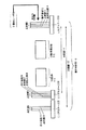
図1に、本発明にかかるパルス光源の第1の実施例を説明する概略図を示す。同図において、反射鏡1と反射鏡2とで形成される共振器1−1(第1の共振器)と反射鏡1と反射鏡3とで形成される共振器1−2(第2の共振器)とが、複合共振器1−3を構成している。また、複合共振器1−3内には、半導体光増幅媒質4(光増幅媒質)と電界吸収型光変調器5(光透過率変調媒質)とが配置されている。反射鏡1及び反射鏡3は、それぞれリニアステージ24及び25(共振長変化手段)により位置を移動できるようになっており、これにより、共振器1−1及び共振器1−2の共振器長を変化させることができる。共振器1−1、共振器1−2、及び半導体光増幅媒質4は、共振器1−1及び共振器1−2内を伝搬する光が少なくとも半導体光増幅媒質4内の一部で偏波面と光軸が一致するように配置されている。なお、電界吸収型光変調器5は共振器1−1あるいは共振器1−2の少なくとも一方の内部に配置されていればよい。
【0019】
半導体光増幅媒質4は、InGaAsP多重量子井戸から成る活性層6と、その上下のクラッド層7及び8と、それらを挟む上下の電極9及び10で構成されている。同様に、電界吸収型光変調器5は、InGaAsP多重量子井戸からなる変調層11と、その上下のクラッド層12及び13と、それらを挟む電極14及び15で構成されている。半導体光増幅媒質4の光導波方向の長さは300μm、電界吸収型光変調器5の光導波方向の長さは100μmとなっている。
【0020】
反射鏡1は、硝子基板16と反射膜17と反射防止膜18とで構成される。反射膜17の反射率は、反射膜の材料及び厚みなどの設計パラメータにより、自由に設定可能であり、ここでは、30%としたが、10〜90%の範囲内の反射率でも利用可能である。反射鏡2は、半導体光増幅媒質4の光出射端面19上の誘電体多層膜20で構成される。誘電体多層膜20の反射率は、ここでは10%としたが、5%から90%の範囲の反射率でも利用可能である。反射鏡3は、硝子基板21と反射膜22により構成される。本実施例では、反射膜22はほぼ100%の反射率としたが、30%以上あれば利用可能である。
【0021】
リニアステージ24及び25は、例えばステッピングモータにより反射鏡1及び反射鏡3の位置が移動できる機能を持つものである。
【0022】
次に、上記の構成により連続可変周波数の高繰り返しパルス列が発生する理由について、図1、図2及び図3を用いて詳細に説明する。
【0023】
共振器1−1においては、半導体光増幅媒質4の電極9から電流注入を行うと、ある閾値電流以上で共振器長に相当するモード間隔でレーザ発振が起こる。このとき、電界吸収型光変調器5の電極14に、逆バイアス電圧と共に共振器1−1の共振器長に相当する共振周波数の高周波電気信号を重畳すると、電界吸収型光変調器5を通過するレーザ光が強度変調される。この強度変調された光が共振器1−1内で往復することで、高周波電気信号に同期した光パルス列が生成される。
【0024】
共振器1−2においても同様に、電界吸収型光変調器5の電極14に、逆バイアス電圧と共に共振器1−2の共振器長に相当する共振周波数の高周波電気信号を重畳すると、共振器1−2の共振器長に相当する共振周波数の高周波電気信号に同期した光パルス列が生成される。
【0025】
ここで、共振器1−1の共振器長を8mm、電界吸収型光変調器5の電極14に印加する高周波電気信号を18.4GHz、共振器1−2の共振器長を13mm、電界吸収型光変調器5の電極14に印加する別の高周波電気信号を11.4GHzとした場合を例に挙げて、複合共振器1−3から発生する光パルス列の繰り返し周波数について説明を行う。
【0026】
図2には、各共振器で発生する縦モードの光周波数特性を示しており、横軸には光周波数、縦軸には光強度を取っている。共振器1−1では、縦モード間隔が18.4GHz、共振器1−2では、11.4GHz間隔と、各共振器長に対応した間隔で縦モードが発生する。そして、複合共振器1−3の効果によって、これらの縦モードをもつ光波が干渉する結果、縦モード位置が一致する1.0488THz間隔の光のみが強調され、複合共振器1−3からは、繰り返し周期1.0488THzの光パルス列が出力される。つまり、各共振器の共振周波数が低くても、複合共振器構成とすることで、高繰り返しの光パルスが生成できる。
【0027】
ここで、リニアステージ24,25により、共振器1−1及び1−2の共振器長を、その共振器1−1の共振器長と共振器1−2の共振器長の比を一定に保ったまま変化させるとともに、変化する共振器長の共振周波数に応じて重畳する高周波電気信号の周波数を変化させると、複合共振器1−3で生成される光パルス列の繰り返し周波数を連続的に変化させることが可能となる。例えば、各共振器長を2倍とした場合、共振器1−1の共振器長は16mm、共振器1−2の共振器長は26mmとなる。この場合、共振器1−1及び共振器1−2の縦モード間隔は、9.2GHzと5.7GHzとなって、複合共振器1−3で生成される光パルス列の繰り返し周波数は、524.4GHzとなる。
【0028】
つぎに、各共振器長を20倍と非常に長くした場合、共振器1−1の共振器長は160mm、共振器1−2の共振器長は260mmとなる。この場合、共振器1−1及び共振器1−2の縦モード間隔は、それぞれ920MHzと570MHzとなって、複合共振器1−3で生成される光パルス列の繰り返し周波数は、52.44GHzとなる。この程度の寸法の共振器であれば、市販のステージを用いて容易に作製でき、さらに長い共振器でも、装置は大がかりとなるが実現可能である。
【0029】
逆に、各共振器長を0.5倍と短くした場合、共振器1−1の共振器長は4mm、共振器1−2の共振器長は6.5mmとなる。これらの共振器長は、半導体光増幅媒質4の光出射端面19及び電界吸収型光変調器5の光出射端面23から出射される光をコリメートするためのレンズの幅2mm、そのレンズのワーキングディスタンス0.3mm、半導体光増幅媒質4と電界吸収型光変調器5の光導波路長の和0.4mm等の、各共振器内に配置される部品の寸法を考えた場合、十分に実現可能な共振器長である。そして、共振器1−1及び共振器1−2の縦モード間隔は、36.8GHzと22.8GHzとなって、複合共振器1−3で生成される光パルス列の繰り返し周波数は2.0976THzとなる。
【0030】
図3は、横軸に複合共振器1−3で生成される光パルス列の繰り返し周波数を、縦軸に共振器長を、対数−対数プロットしたものである。繰り返し周波数と共振器長との関係が、対数−対数グラフで直線となっているのは、各共振器長をn倍とすると、繰り返し周波数は、1/nとなるからである。これにより、繰り返し周波数は連続的に変化できることがわかる。
【0031】
以上述べたような構成において、共振器1−1及び共振器1−2の長さの比を保ったまま、各共振器長を変化させることで、光パルス列の繰り返し周波数は50GHzから2THz程度まで連続的に変化させることができる。
【0032】
なお、本実施例では、反射鏡1〜3として誘電体多層膜20や硝子基板上に形成した反射膜17及び22を用いたが、半導体のブラッグ反射鏡でも、ファイバグレーティングでも構成できる。
【0033】
また、半導体光増幅媒質4として、InGaAsP多重量子井戸から成る活性層6を用いたが、GaAs/AlGaAsの量子井戸や、GaN/AlGaNの量子井戸の活性層でもよい。
【0034】
また、光透過率変調媒質として、電界吸収型光変調器5を用いたが、可飽和吸収体を逆バイアスで用いても良いし、リチウム酸ニオブ強度変調器で構成しても良いし、半導体光増幅媒質4の注入電流を変調して用いてもよい。後者の場合は半導体光増幅媒質4のみでレーザ発生と光強度変調を兼ねさせ、電界吸収方光変調器5を削除することができる。
【0035】
なお、第1の実施例を示す図1では、図面を省略するため、半導体光増幅媒質4の光出射端面19及び電界吸収型光変調器5の光出射端面23から出射される光をコリメートするためのレンズは省いている。
【0036】
[第2の実施例]
図4に、本発明にかかるパルス光源の第2の実施例を説明する概略図を示す。第2の実施例の構成は、第1の実施例の構成とほぼ同じであるが、半導体光増幅媒質4の代わりに、YAG結晶4−2(光増幅媒質)を用い、電界吸収型光変調器5の代わりに、リチウム酸ニオブ強度変調器5−2(光透過率変調媒質)を用いている。また、反射鏡2として、誘電体多層膜20の代わりに、硝子基板26と反射膜27と反射防止膜28とで構成される反射鏡2を用いている。さらに、この反射鏡2を動かすリニアステージ29が追加されている。ただし、半導体光増幅媒質4の代わりに用いているYAG結晶4−2は、電流注入による光増幅ができないので、外部の半導体レーザ30からの入力によって光励起する必要がある。
【0037】
ここで、共振器1−1の共振器長を55mm、リチウム酸ニオブ強度変調器5−2に印加する高周波電気信号を1.07GHz、共振器1−2の共振器長を65mm、リチウム酸ニオブ強度変調器5−2に印加する別の高周波電気信号を0.94GHzとした場合、複合共振器の効果により、複合共振器1−3からは、繰り返し周期100.58GHzの光パルス列が出力される。第1の実施例で述べたように、各共振器長を、比を一定に保ったまま変化させるとともに、変化する共振器長の共振周波数に応じて、重畳する高周波電気信号の周波数を変化させると、複合共振器1−3で生成される光パルス列の繰り返し周波数を連続的に変化させることが可能となる。
【0038】
なお、第2の実施例を示す図4では、図面を省略するため、リチウム酸ニオブ強度変調器5−2から出射される光をコリメートするためのレンズなどの光学部品は省いている。
【0039】
【発明の効果】
以上説明したように、本発明のパルス光源によれば、安定で高繰り返しの連続光パルスを発生でき、しかも繰り返し周波数を精度良く自由に変えることができ、実用的に非常に有用なパルス光源を提供することができる。
【図面の簡単な説明】
【図1】本発明によるパルス光源の第1の実施例の構成を示す図である。
【図2】複合共振器の効果を説明する説明図である。
【図3】繰り返し周波数と共振器長との関係を示す特性図である。
【図4】本発明によるパルス光源の第2の実施例の構成を示す図である。
【図5】従来の周波数可変な光パルス光源の構成を示す図である。
【符号の説明】1−1:共振器、1−2:共振器、1−3:複合共振器、1:反射鏡、2:反射鏡、3:反射鏡、4:半導体光増幅媒質、5:電界吸収型光変調器、6:活性層、7:クラッド層、8:クラッド層、9:電極、10:電極、11:変調層、12:クラッド層、13:クラッド層、14:電極、15:電極、16:硝子基板、17:反射膜、18:反射防止膜、19:光出射端面、20:誘電体多層膜、21:硝子基板、22:反射膜、23:光出射端面、24:リニアステージ、25:リニアステージ、4−2:YAG結晶、5−2:リチウム酸ニオブ強度変調器、26:硝子基板:27:反射膜、28:反射防止膜、29:リニアステージ、30:半導体レーザ、41:レーザ、42:レーザ、43a,43b:光路、44a,44b:光路、45:偏波コントローラ、46:偏波コントローラ、47:光カプラ、48:光路、49:ビート光[0001]
TECHNICAL FIELD OF THE INVENTION
The present invention relates to a pulse light source that can change a repetition frequency.
[0002]
[Prior art]
The pulse light source plays a very important role in various technical fields utilizing the broadband characteristics of light, such as optical measurement and optical communication. Particularly, in recent years, a pulse light source that generates a continuous pulse train having a high repetition frequency exceeding 100 GHz has been used as a light source used for ultra-high-speed optical communication, a millimeter-wave signal source combined with a photoelectric conversion element, and the like.
[0003]
A typical example of a pulsed light source is a mode-locked laser that can generate a very short optical pulse.A semiconductor mode-locked laser has a higher repetition pulse than a mode-locked laser using a solid-state laser or a gas laser. It has the advantage that it can be generated, is small and has excellent stability. At present, a semiconductor mode-locked laser having a repetition frequency from several GHz to about 100 GHz has been reported. However, since a part of the semiconductor material is usually processed by cleavage or the like to form a reflecting mirror, the cavity length is fixed. Therefore, there is a problem that the repetition frequency cannot be changed continuously. For example,
[0004]
Further, in order to obtain a higher repetition frequency, an attempt has been made to provide a third reflecting mirror by forming a groove or the like inside a resonator of a semiconductor laser to utilize the composite resonator effect (Non-Patent Document 3). ). The complex resonator effect is to generate light with a large vertical mode interval by interference between longitudinal modes generated by a plurality of resonators. By adopting such a configuration, it is possible to realize a high repetition frequency, but also in this case, since a part of the semiconductor material is processed to form a reflecting mirror, it is necessary to change the repetition frequency. There was a problem that can not be.
[0005]
Conventionally, there is a beat light source as shown in FIG. 5 as a pulse light source capable of freely changing the repetition frequency. In this method, output lights of two
[0006]
In this method, the frequency of the
[0007]
Further, there is a method using a light source having a configuration in which one of the reflecting mirrors of a semiconductor mode-locked laser is replaced with an external reflecting mirror as disclosed in Non-Patent Document 4. In the light source having this configuration, an optical pulse train with a variable repetition frequency can be generated by moving the external reflecting mirror to change the resonator length. However, when generating an optical pulse train having a basic resonance frequency corresponding to the length of the resonator, the upper limit of the repetition frequency is about 40 GHz because the length of the resonator is limited by the dimensions of the optical components used. Also, by synchronizing with an electrical signal that is an integral multiple of the fundamental resonance frequency, a repetitive pulse train up to about 80 GHz can be generated. However, it is difficult to generate a high-repetition optical pulse train exceeding 100 GHz due to limitations of electronics. Was.
[0008]
[Non-Patent Document 1] Hansen PB, Ray-Bon G, Koren U, Mirror BI, Young MG, Cien M, Vals CA, Alphaness RC, "5.5 mm InGaAs monolithic including integrated Bragg reflector for active mode locking""Extended Cavity Laser", IEEE, Optical Technology, Vol. 4, 8, March 1992, pp. 215-217 ("5.5 nm Long InGaAsP Monolithic Extended-Cavity Laser With an Integrated Bragg-Referential Mirror for Ref. , PB, Raybon, G., Koren, U., Miler, BI, Young, MG, Chien, M., Burrus, CA, Alfern. ess, RC, IEEE Photon. Technol.).
[0009]
[Non-Patent Document 2] Sato K, Kotaka I, Hirano A, Asobe M, Miyamoto Y, Shimizu N, Hagimoto K, "High repetition frequency pulse at 102 GHz using mode-locked laser with integrated electroabsorption modulator." Generation, "Electronic Letters, Vol. 34, 8 April 16, 1998, pp. 790-792 (" High-repetition frequency pulse generation at 102 GHz using modelocked lasers integrated with K.A., K.A., K.K., K.K. Hirano, A., Asobe, M., Miyamoto, Y., Shimizu, N., Hagimoto, K., Electro. n. Lett., vol.34, 8, 16 April 1998, pp. 790-792.).
[0010]
[Non-Patent Document 3] Jansson DA, Street MW, McDoull SD, Tanny IG, Marsh JH, Abratin EA, "Ultrafast Harmonic Mode Lock of Monolithic Composite Cavity Laser Diode Using Photonic Bandgap Mirror", IEEE J. Quantum Electronics Letter, Vol. 38, 1, January 1, 2002, pp. 1-11 ("Ultrafast Harmonic Mode-Locking of Monolithic Compound-Cavity Laser Diodes Corporation, Canada, Canada, Canada, USA). , MW, McDougall, SD, Thayne, IG, Marsh, JH. Avrutin, E.A., IEEE J. Quantumn Electron.Lett., Vo1.38,1,1 Jan. 2002, pp.1-11.).
[0011]
[Non-Patent Document 4] Hashimoto Y, Yamada H, Kuribayashi R, Yokoyama, "40 GHz tunable optical pulse generation by highly stable external cavity mode-locked semiconductor laser module", OFC, 2002, WV5, pp. 342-343 (""). 40-GHz Tunable Optical Pulse Generation from a Highly-Stable External-Cavity Mode-Locked Semiconductor Laser Laser Module, 200, Y.a., Y.a., Y.a., Y.a., Y.a. .).
[0012]
[Problems to be solved by the invention]
As described above, in the conventional pulse light source technology, it has been difficult to realize a pulse light source that can change the repetition frequency with high accuracy to a stable and high frequency.
[0013]
SUMMARY OF THE INVENTION An object of the present invention is to provide a variable frequency pulse light source that can control a repetition frequency from 100 GHz to several THz with high accuracy, which is difficult to realize with the conventional technology.
[0014]
[Means for Solving the Invention]
The invention according to
[0015]
In the pulse light source according to claim 2 or
[0016]
According to a third aspect of the present invention, in the pulse light source according to the first or second aspect, the light transmittance modulating medium comprises: an electric signal having a resonance frequency corresponding to a resonator length of the first resonator; The pulse light source is characterized in that an electric signal of a resonance frequency corresponding to the resonator length of the second resonator is superimposed and applied.
[0017]
According to a fourth aspect of the present invention, in the pulse light source according to the first, second or third aspect, the light transmittance modulating medium is also used as the light amplifying medium, and modulation is performed by a current injected into the light amplifying medium. A pulsed light source characterized in that:
[0018]
BEST MODE FOR CARRYING OUT THE INVENTION
[First Embodiment]
FIG. 1 is a schematic diagram illustrating a pulse light source according to a first embodiment of the present invention. In the figure, a resonator 1-1 (first resonator) formed by a
[0019]
The semiconductor optical amplifying medium 4 includes an active layer 6 made of InGaAsP multiple quantum well, upper and lower cladding layers 7 and 8, and upper and
[0020]
The reflecting
[0021]
The
[0022]
Next, the reason why a high repetition pulse train having a continuously variable frequency is generated by the above configuration will be described in detail with reference to FIGS. 1, 2 and 3. FIG.
[0023]
In the resonator 1-1, when current is injected from the
[0024]
Similarly, in the resonator 1-2, when a high-frequency electric signal having a resonance frequency corresponding to the resonator length of the resonator 1-2 is superimposed on the electrode 14 of the electroabsorption optical modulator 5 together with the reverse bias voltage. An optical pulse train synchronized with a high-frequency electric signal having a resonance frequency corresponding to the resonator length of 1-2 is generated.
[0025]
Here, the resonator length of the resonator 1-1 is 8 mm, the high-frequency electric signal applied to the electrode 14 of the electroabsorption optical modulator 5 is 18.4 GHz, the resonator length of the resonator 1-2 is 13 mm, and the electric field absorption is performed. The repetition frequency of the optical pulse train generated from the composite resonator 1-3 will be described using an example in which another high-frequency electric signal applied to the electrode 14 of the optical modulator 5 is 11.4 GHz.
[0026]
FIG. 2 shows the optical frequency characteristics of the longitudinal mode generated in each resonator, with the horizontal axis representing the optical frequency and the vertical axis representing the light intensity. In the resonator 1-1, a longitudinal mode interval is generated at 18.4 GHz, and in the resonator 1-2, a longitudinal mode is generated at an interval corresponding to each resonator length of 11.4 GHz. Then, due to the effect of the composite resonator 1-3, the light waves having these longitudinal modes interfere with each other. As a result, only the light at the interval of 1.0488 THz at which the longitudinal mode position coincides is emphasized. An optical pulse train having a repetition period of 1.0488 THz is output. That is, even if the resonance frequency of each resonator is low, a high repetition optical pulse can be generated by using the composite resonator configuration.
[0027]
Here, the
[0028]
Next, when the length of each resonator is very long, ie, 20 times, the resonator length of the resonator 1-1 is 160 mm and the resonator length of the resonator 1-2 is 260 mm. In this case, the longitudinal mode intervals of the resonator 1-1 and the resonator 1-2 are 920 MHz and 570 MHz, respectively, and the repetition frequency of the optical pulse train generated by the composite resonator 1-3 is 52.44 GHz. . A resonator having such a size can be easily manufactured using a commercially available stage, and a longer resonator can be realized with a large-scale device.
[0029]
Conversely, when the length of each resonator is reduced to 0.5 times, the length of the resonator 1-1 is 4 mm, and the length of the resonator 1-2 is 6.5 mm. These resonator lengths are 2 mm in width of a lens for collimating light emitted from the light emitting end face 19 of the semiconductor optical amplification medium 4 and the light emitting end face 23 of the electro-absorption optical modulator 5, and the working distance of the lens Considering the dimensions of the components arranged in each resonator, such as 0.3 mm and the sum of the optical waveguide lengths of the semiconductor optical amplification medium 4 and the electro-absorption optical modulator 5 of 0.4 mm, etc., it can be realized sufficiently. Resonator length. The longitudinal mode interval between the resonator 1-1 and the resonator 1-2 is 36.8 GHz and 22.8 GHz, and the repetition frequency of the optical pulse train generated by the composite resonator 1-3 is 2.0976 THz. Become.
[0030]
FIG. 3 is a log-log plot of the repetition frequency of the optical pulse train generated by the composite resonator 1-3 on the horizontal axis and the resonator length on the vertical axis. The relationship between the repetition frequency and the resonator length is a straight line in the logarithmic-logarithmic graph because, if each resonator length is n times, the repetition frequency is 1 / n. This indicates that the repetition frequency can be changed continuously.
[0031]
In the configuration as described above, the repetition frequency of the optical pulse train is changed from about 50 GHz to about 2 THz by changing the length of each resonator while maintaining the length ratio between the resonators 1-1 and 1-2. It can be changed continuously.
[0032]
In the present embodiment, the dielectric multilayer films 20 and the reflection films 17 and 22 formed on the glass substrate are used as the reflection mirrors 1 to 3. However, a semiconductor Bragg reflection mirror or a fiber grating can be used.
[0033]
Further, although the active layer 6 made of InGaAsP multiple quantum well is used as the semiconductor optical amplifying medium 4, an active layer of GaAs / AlGaAs quantum well or GaN / AlGaN quantum well may be used.
[0034]
Although the electro-absorption optical modulator 5 is used as a light transmittance modulation medium, a saturable absorber may be used with a reverse bias, a niobium lithium niobate intensity modulator may be used, or a semiconductor may be used. The injection current of the optical amplification medium 4 may be modulated and used. In the latter case, laser generation and light intensity modulation can be performed only by the semiconductor optical amplifying medium 4, and the electroabsorption optical modulator 5 can be omitted.
[0035]
In FIG. 1 showing the first embodiment, the light emitted from the light emitting end face 19 of the semiconductor optical amplifying medium 4 and the light emitting end face 23 of the electro-absorption optical modulator 5 are collimated for omitting the drawing. The lens for it is omitted.
[0036]
[Second embodiment]
FIG. 4 is a schematic diagram illustrating a pulse light source according to a second embodiment of the present invention. The configuration of the second embodiment is almost the same as the configuration of the first embodiment, except that a YAG crystal 4-2 (optical amplification medium) is used instead of the semiconductor optical amplification medium 4 and an electro-absorption type optical modulation. Instead of the device 5, a niobium lithium oxide intensity modulator 5-2 (light transmittance modulation medium) is used. Further, as the reflecting mirror 2, instead of the dielectric multilayer film 20, the reflecting mirror 2 composed of a glass substrate 26, a reflecting film 27 and an anti-reflection film 28 is used. Further, a linear stage 29 for moving the reflecting mirror 2 is added. However, since the YAG crystal 4-2 used in place of the semiconductor optical amplification medium 4 cannot perform optical amplification by current injection, it must be optically pumped by an input from an external semiconductor laser 30.
[0037]
Here, the resonator length of the resonator 1-1 is 55 mm, the high frequency electric signal applied to the niobium lithium niobate intensity modulator 5-2 is 1.07 GHz, the resonator length of the resonator 1-2 is 65 mm, and the niobium lithium niobate is used. When another high-frequency electric signal applied to the intensity modulator 5-2 is 0.94 GHz, an optical pulse train having a repetition period of 100.58 GHz is output from the composite resonator 1-3 due to the effect of the composite resonator. . As described in the first embodiment, while changing the length of each resonator while keeping the ratio constant, the frequency of the high-frequency electric signal to be superimposed is changed according to the resonance frequency of the changing resonator length. Thus, it is possible to continuously change the repetition frequency of the optical pulse train generated by the composite resonator 1-3.
[0038]
In FIG. 4 showing the second embodiment, optical parts such as a lens for collimating the light emitted from the niobium lithium niobate intensity modulator 5-2 are omitted for omitting the drawing.
[0039]
【The invention's effect】
As described above, according to the pulse light source of the present invention, a stable and highly repetitive continuous light pulse can be generated, and the repetition frequency can be freely changed with high accuracy. Can be provided.
[Brief description of the drawings]
FIG. 1 is a diagram showing the configuration of a first embodiment of a pulse light source according to the present invention.
FIG. 2 is an explanatory diagram illustrating an effect of the composite resonator.
FIG. 3 is a characteristic diagram showing a relationship between a repetition frequency and a resonator length.
FIG. 4 is a diagram showing a configuration of a pulse light source according to a second embodiment of the present invention.
FIG. 5 is a diagram showing a configuration of a conventional frequency-variable optical pulse light source.
DESCRIPTION OF SYMBOLS 1-1: resonator, 1-2: resonator, 1-3: composite resonator, 1: reflecting mirror, 2: reflecting mirror, 3: reflecting mirror, 4: semiconductor optical amplification medium, 5 : Electroabsorption optical modulator, 6: active layer, 7: clad layer, 8: clad layer, 9: electrode, 10: electrode, 11: modulation layer, 12: clad layer, 13: clad layer, 14: electrode, Reference numeral 15: electrode, 16: glass substrate, 17: reflection film, 18: antireflection film, 19: light-emitting end face, 20: dielectric multilayer film, 21: glass substrate, 22: reflection film, 23: light-emitting end face, 24 : Linear stage, 25: linear stage, 4-2: YAG crystal, 5-2: niobium lithium oxide intensity modulator, 26: glass substrate: 27: reflection film, 28: antireflection film, 29: linear stage, 30: Semiconductor laser, 41: laser, 42: laser, 43a, 43b: optical path, 44 , 44b: light path, 45: a polarization controller, 46: a polarization controller, 47: an optical coupler, 48: optical path, 49: beat light
Claims (4)
前記第2の反射鏡の前記第1の反射鏡と反対側に配置された第3の反射鏡と前記第1の反射鏡とからなる第2の共振器と、
前記第1の共振器と前記第2の共振器の内部に共有される光増幅媒質と、
前記第1の共振器あるいは前記第2の共振器の少なくとも一方の内部に配置された光透過率変調媒質と、
前記第1の共振器及び前記第2の共振器の共振長を連動して変化させる共振長変化手段と、を具備し、
前記第1の共振器、第2の共振器及び前記光増幅媒質は、前記第1の共振器及び前記第2の共振器内を伝搬する光が少なくとも前記光増幅媒質内の一部で偏波面と光軸が一致するようにが配置されている、
ことを特徴とするパルス光源。A first resonator including a first reflecting mirror and a second reflecting mirror;
A second resonator composed of a third reflector and the first reflector disposed on the second reflector opposite to the first reflector;
An optical amplifying medium shared inside the first resonator and the second resonator;
A light transmittance modulation medium disposed inside at least one of the first resonator and the second resonator;
Resonance length changing means for changing the resonance length of the first resonator and the second resonator in an interlocked manner,
The first resonator, the second resonator, and the optical amplifying medium may be configured such that light propagating in the first resonator and the second resonator is polarized at least in a part of the optical amplifying medium. And are arranged so that the optical axis matches,
A pulsed light source characterized in that:
前記共振長変化手段は、前記第1の共振器及び前記第2の共振器の共振長を、その比を一定に保持して変化させることを特徴とするパルス光源。The pulse light source according to claim 1,
A pulse light source, wherein the resonance length changing means changes the resonance length of the first resonator and the second resonator while keeping the ratio constant.
前記光透過率変調媒質は、前記第1の共振器の共振器長に相当する共振周波数の電気信号と、前記第2の共振器の共振器長に相当する共振周波数の電気信号とが重畳されて印加されるようにしたことを特徴とするパルス光源。The pulse light source according to claim 1 or 2,
In the light transmittance modulation medium, an electric signal having a resonance frequency corresponding to the resonator length of the first resonator and an electric signal having a resonance frequency corresponding to the resonator length of the second resonator are superimposed. A pulsed light source characterized in that the pulsed light is applied.
前記光透過率変調媒質を前記光増幅媒質で兼ねさせ、前記光増幅媒質に注入する電流により変調を行うようにしたことを特徴とするパルス光源。The pulse light source according to claim 1, 2 or 3,
A pulse light source, wherein the light transmittance modulation medium is also used as the light amplification medium, and modulation is performed by a current injected into the light amplification medium.
Priority Applications (1)
| Application Number | Priority Date | Filing Date | Title |
|---|---|---|---|
| JP2003161575A JP2004363419A (en) | 2003-06-06 | 2003-06-06 | Pulsed light source |
Applications Claiming Priority (1)
| Application Number | Priority Date | Filing Date | Title |
|---|---|---|---|
| JP2003161575A JP2004363419A (en) | 2003-06-06 | 2003-06-06 | Pulsed light source |
Publications (1)
| Publication Number | Publication Date |
|---|---|
| JP2004363419A true JP2004363419A (en) | 2004-12-24 |
Family
ID=34053952
Family Applications (1)
| Application Number | Title | Priority Date | Filing Date |
|---|---|---|---|
| JP2003161575A Withdrawn JP2004363419A (en) | 2003-06-06 | 2003-06-06 | Pulsed light source |
Country Status (1)
| Country | Link |
|---|---|
| JP (1) | JP2004363419A (en) |
Cited By (8)
| Publication number | Priority date | Publication date | Assignee | Title |
|---|---|---|---|---|
| JP2009130356A (en) * | 2007-11-20 | 2009-06-11 | Itt Manufacturing Enterprises Inc | Method and device for generating rgb laser light |
| JP2018518836A (en) * | 2015-05-20 | 2018-07-12 | クアンタム−エスアイ インコーポレイテッドQuantum−Si Incorporated | Pulsed laser and biological analysis system |
| US10741990B2 (en) | 2016-12-16 | 2020-08-11 | Quantum-Si Incorporated | Compact mode-locked laser module |
| US11249318B2 (en) | 2016-12-16 | 2022-02-15 | Quantum-Si Incorporated | Compact beam shaping and steering assembly |
| US11466316B2 (en) | 2015-05-20 | 2022-10-11 | Quantum-Si Incorporated | Pulsed laser and bioanalytic system |
| US11567006B2 (en) | 2015-05-20 | 2023-01-31 | Quantum-Si Incorporated | Optical sources for fluorescent lifetime analysis |
| US11747561B2 (en) | 2019-06-14 | 2023-09-05 | Quantum-Si Incorporated | Sliced grating coupler with increased beam alignment sensitivity |
| US11808700B2 (en) | 2018-06-15 | 2023-11-07 | Quantum-Si Incorporated | Data acquisition control for advanced analytic instruments having pulsed optical sources |
-
2003
- 2003-06-06 JP JP2003161575A patent/JP2004363419A/en not_active Withdrawn
Cited By (10)
| Publication number | Priority date | Publication date | Assignee | Title |
|---|---|---|---|---|
| JP2009130356A (en) * | 2007-11-20 | 2009-06-11 | Itt Manufacturing Enterprises Inc | Method and device for generating rgb laser light |
| JP2018518836A (en) * | 2015-05-20 | 2018-07-12 | クアンタム−エスアイ インコーポレイテッドQuantum−Si Incorporated | Pulsed laser and biological analysis system |
| US11466316B2 (en) | 2015-05-20 | 2022-10-11 | Quantum-Si Incorporated | Pulsed laser and bioanalytic system |
| US11567006B2 (en) | 2015-05-20 | 2023-01-31 | Quantum-Si Incorporated | Optical sources for fluorescent lifetime analysis |
| US10741990B2 (en) | 2016-12-16 | 2020-08-11 | Quantum-Si Incorporated | Compact mode-locked laser module |
| US11249318B2 (en) | 2016-12-16 | 2022-02-15 | Quantum-Si Incorporated | Compact beam shaping and steering assembly |
| US11322906B2 (en) | 2016-12-16 | 2022-05-03 | Quantum-Si Incorporated | Compact mode-locked laser module |
| US11848531B2 (en) | 2016-12-16 | 2023-12-19 | Quantum-Si Incorporated | Compact mode-locked laser module |
| US11808700B2 (en) | 2018-06-15 | 2023-11-07 | Quantum-Si Incorporated | Data acquisition control for advanced analytic instruments having pulsed optical sources |
| US11747561B2 (en) | 2019-06-14 | 2023-09-05 | Quantum-Si Incorporated | Sliced grating coupler with increased beam alignment sensitivity |
Similar Documents
| Publication | Publication Date | Title |
|---|---|---|
| JP2973943B2 (en) | Mode-locked semiconductor laser and method of driving the same | |
| JP2007005594A (en) | Semiconductor optical element and module using same | |
| JPH04229674A (en) | Optical device | |
| US20040190567A1 (en) | Optically pumped laser device for generating laser pulses | |
| EP3425755B1 (en) | Surface light emitting laser | |
| JP2004363419A (en) | Pulsed light source | |
| JP2018060974A (en) | Semiconductor optical integrated element | |
| JP5001239B2 (en) | Semiconductor tunable laser | |
| Shamim et al. | Single and multiple longitudinal wavelength generation in green diode lasers | |
| RU2540233C1 (en) | Injection laser having multiwave modulated emission | |
| JP2005512136A (en) | Optical microwave source | |
| JP3227701B2 (en) | Mode-locked semiconductor laser | |
| JP2005159118A (en) | Milliwave light source | |
| JPH0595152A (en) | Semiconductor short optical pulse generator and generating method for short optical pulse | |
| Li et al. | Wavelength tunable high-power single-mode 1060-nm DBR lasers | |
| Choquette et al. | Coupled-resonator vertical-cavity laser | |
| Rafailov et al. | Nonresonant self-injection seeding of a gain-switched diode laser | |
| JP2004158590A (en) | Semiconductor pulsed light source | |
| Mahnkopf et al. | Widely tunable complex-coupled distributed feedback laser with photonic crystal mirrors and integrated optical amplifier | |
| CN114284861B (en) | Photon integrated chaotic laser based on mutual injection combined distributed grating feedback | |
| JP2018060973A (en) | Semiconductor optical integrated element and optical transmission/reception module mounted with the same | |
| Kim et al. | Optical characteristics of 1.3-µm dual-mode laser diode with integrated semiconductor optical amplifier | |
| JPH05160519A (en) | Very short light pulse generating device | |
| Hargreaves et al. | Residual phase-noise measurements of actively mode-locked fiber and semiconductor lasers | |
| Guina et al. | Saturable absorber intensity modulator |
Legal Events
| Date | Code | Title | Description |
|---|---|---|---|
| A300 | Application deemed to be withdrawn because no request for examination was validly filed |
Free format text: JAPANESE INTERMEDIATE CODE: A300 Effective date: 20060905 |