JP2004363085A - Inspection apparatus by charged particle beam and method for manufacturing device using inspection apparatus - Google Patents
Inspection apparatus by charged particle beam and method for manufacturing device using inspection apparatus Download PDFInfo
- Publication number
- JP2004363085A JP2004363085A JP2004031749A JP2004031749A JP2004363085A JP 2004363085 A JP2004363085 A JP 2004363085A JP 2004031749 A JP2004031749 A JP 2004031749A JP 2004031749 A JP2004031749 A JP 2004031749A JP 2004363085 A JP2004363085 A JP 2004363085A
- Authority
- JP
- Japan
- Prior art keywords
- electron beam
- electrons
- sample
- image
- detector
- Prior art date
- Legal status (The legal status is an assumption and is not a legal conclusion. Google has not performed a legal analysis and makes no representation as to the accuracy of the status listed.)
- Pending
Links
Images


Classifications
-
- G—PHYSICS
- G01—MEASURING; TESTING
- G01N—INVESTIGATING OR ANALYSING MATERIALS BY DETERMINING THEIR CHEMICAL OR PHYSICAL PROPERTIES
- G01N23/00—Investigating or analysing materials by the use of wave or particle radiation, e.g. X-rays or neutrons, not covered by groups G01N3/00 – G01N17/00, G01N21/00 or G01N22/00
- G01N23/22—Investigating or analysing materials by the use of wave or particle radiation, e.g. X-rays or neutrons, not covered by groups G01N3/00 – G01N17/00, G01N21/00 or G01N22/00 by measuring secondary emission from the material
- G01N23/225—Investigating or analysing materials by the use of wave or particle radiation, e.g. X-rays or neutrons, not covered by groups G01N3/00 – G01N17/00, G01N21/00 or G01N22/00 by measuring secondary emission from the material using electron or ion
-
- H—ELECTRICITY
- H01—ELECTRIC ELEMENTS
- H01L—SEMICONDUCTOR DEVICES NOT COVERED BY CLASS H10
- H01L22/00—Testing or measuring during manufacture or treatment; Reliability measurements, i.e. testing of parts without further processing to modify the parts as such; Structural arrangements therefor
-
- H—ELECTRICITY
- H01—ELECTRIC ELEMENTS
- H01J—ELECTRIC DISCHARGE TUBES OR DISCHARGE LAMPS
- H01J37/00—Discharge tubes with provision for introducing objects or material to be exposed to the discharge, e.g. for the purpose of examination or processing thereof
- H01J37/02—Details
- H01J37/04—Arrangements of electrodes and associated parts for generating or controlling the discharge, e.g. electron-optical arrangement, ion-optical arrangement
- H01J37/05—Electron or ion-optical arrangements for separating electrons or ions according to their energy or mass
-
- H—ELECTRICITY
- H01—ELECTRIC ELEMENTS
- H01J—ELECTRIC DISCHARGE TUBES OR DISCHARGE LAMPS
- H01J37/00—Discharge tubes with provision for introducing objects or material to be exposed to the discharge, e.g. for the purpose of examination or processing thereof
- H01J37/26—Electron or ion microscopes; Electron or ion diffraction tubes
- H01J37/28—Electron or ion microscopes; Electron or ion diffraction tubes with scanning beams
-
- H—ELECTRICITY
- H01—ELECTRIC ELEMENTS
- H01J—ELECTRIC DISCHARGE TUBES OR DISCHARGE LAMPS
- H01J2237/00—Discharge tubes exposing object to beam, e.g. for analysis treatment, etching, imaging
- H01J2237/244—Detection characterized by the detecting means
- H01J2237/2441—Semiconductor detectors, e.g. diodes
-
- H—ELECTRICITY
- H01—ELECTRIC ELEMENTS
- H01J—ELECTRIC DISCHARGE TUBES OR DISCHARGE LAMPS
- H01J2237/00—Discharge tubes exposing object to beam, e.g. for analysis treatment, etching, imaging
- H01J2237/244—Detection characterized by the detecting means
- H01J2237/2446—Position sensitive detectors
-
- H—ELECTRICITY
- H01—ELECTRIC ELEMENTS
- H01J—ELECTRIC DISCHARGE TUBES OR DISCHARGE LAMPS
- H01J2237/00—Discharge tubes exposing object to beam, e.g. for analysis treatment, etching, imaging
- H01J2237/26—Electron or ion microscopes
- H01J2237/28—Scanning microscopes
- H01J2237/2813—Scanning microscopes characterised by the application
- H01J2237/2817—Pattern inspection
Abstract
Description
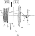
本発明は、電子ビームを用いて検査対象の表面に形成されたパターンの欠陥等を検査する検査装置に関し、詳しくは、半導体製造工程におけるウェーハの欠陥を検出する場合のように、電子ビームを検査対象に照射してその表面の性状に応じて変化する二次電子を捕捉して画像データを形成し、その画像データに基づいて検査対象の表面に形成されたパターン等を高いスループットで検査する検査装置、並びにそのような検査装置を用いて歩留まり良くデバイスを製造するデバイス製造方法に関する。より具体的には、面ビームを用いた写像投影方式による検出装置および該装置を用いたデバイス製造方法に関する。 The present invention relates to an inspection apparatus for inspecting a defect or the like of a pattern formed on a surface of an inspection object using an electron beam, and more particularly, to inspecting an electron beam as in the case of detecting a defect of a wafer in a semiconductor manufacturing process. Inspection that irradiates an object and captures secondary electrons that change according to the surface properties to form image data, and inspects patterns, etc., formed on the surface of the inspection object with high throughput based on the image data The present invention relates to an apparatus and a device manufacturing method for manufacturing a device with a high yield using such an inspection apparatus. More specifically, the present invention relates to a detection device based on a projection method using a surface beam and a device manufacturing method using the detection device.
半導体プロセスにおいて、デザインルールは100nmの時代を迎えようとしており、また生産形態はDRAMに代表される少品種大量生産からSOC(Silicon on chip)のように多品種少量生産へ移行しつつある。それに伴い、製造工程数が増加し、各工程毎の歩留まり向上は必須となり、プロセス起因の欠陥検査が重要になる。本発明は半導体プロセスにおける各工程後のウェーハ等の検査に用いられる装置に関し、電子ビームを用いた検査方法及び装置またはそれを用いたデバイス製造方法に関する。 In the semiconductor process, the design rule is approaching the era of 100 nm, and the production form is shifting from small-kind mass production represented by DRAM to multi-kind small production such as SOC (Silicon on chip). As a result, the number of manufacturing steps increases, and it is essential to improve the yield for each step, and defect inspection due to the process becomes important. The present invention relates to an apparatus used for inspection of a wafer or the like after each step in a semiconductor process, and relates to an inspection method and an apparatus using an electron beam or a device manufacturing method using the same.
半導体デバイスの高集積化、パターンの微細化に伴い、高分解能、高スループットの検査装置が要求されている。100nmデザインルールのウェーハ基板の欠陥を調べるためには、100nm以下の線幅を有する配線におけるパターン欠陥やパーティクル・ビアの欠陥及びこれらの電気的欠陥を見る必要があり、したがって100nm以下の分解能が必要であり、デバイスの高集積化による製造工程の増加により、検査量が増大するため、高スループットが要求されている。また、デバイスの多層化が進むにつれて、層間の配線をつなぐビアのコンタクト不良(電気的欠陥)を検出する機能も、検査装置に要求されている。現在は主に光方式の欠陥検査装置が使用されているが、分解能及びコンタクト不良検査の点では、光方式の欠陥検査装置に代わって、電子ビームを用いた欠陥検査装置が今後は検査装置の主流になると予想される。ただし、電子ビーム方式欠陥検査装置にも弱点があり、それはスループットの点で光方式に劣ることである。 2. Description of the Related Art As semiconductor devices become highly integrated and patterns become finer, high-resolution and high-throughput inspection apparatuses are required. In order to investigate defects on a wafer substrate with a design rule of 100 nm, it is necessary to see pattern defects, defects of particle vias, and electrical defects of wiring having a line width of 100 nm or less, and therefore, a resolution of 100 nm or less is required. In addition, since the number of inspections increases due to an increase in the number of manufacturing steps due to high integration of devices, high throughput is required. In addition, as devices become more multi-layered, inspection devices are also required to have a function of detecting a contact failure (electrical defect) of a via connecting an interlayer wiring. At present, optical defect inspection equipment is mainly used, but in terms of resolution and contact defect inspection, defect inspection equipment using electron beams will replace optical optical defect inspection equipment in the future. It is expected to become mainstream. However, the electron beam type defect inspection apparatus also has a weak point, which is inferior to the optical type in terms of throughput.
このため、高分解能、高スループット、且つ電気的欠陥検出が可能な検査装置の開発が要求されている。光方式での分解能は使用する光の波長の1/2が限界と言われており、実用化されている可視光の例では0.2μm程度である。 For this reason, there is a demand for the development of a high-resolution, high-throughput inspection apparatus capable of detecting electrical defects. It is said that the resolution in the optical system is limited to 1/2 of the wavelength of the light used, and is about 0.2 μm in the case of practically used visible light.
一方、電子ビームを使用する方式では、通常、走査型電子ビーム方式(SEM方式)が実用化されており、分解能は0.1μm、検査時間は8時間/枚(200mmウェーハ)である。電子ビーム方式はまた、電気的欠陥(配線の断線、導通不良、ビアの導通不良等)も検査可能であることが大きな特徴であるが、検査速度が非常に遅く、検査速度の速い欠陥検査装置の開発が期待されている。 On the other hand, as a method using an electron beam, a scanning electron beam method (SEM method) is usually put into practical use, and the resolution is 0.1 μm and the inspection time is 8 hours / sheet (200 mm wafer). The electron beam method is also characterized in that it can inspect electrical defects (such as disconnection of wiring, poor conduction, poor conduction of vias, etc.), but the defect inspection device has a very low inspection speed and a high inspection speed. The development of is expected.
一般に、検査装置は高価であり、またスループットも他のプロセス装置に比べて低いために、現状では重要な工程の後、例えばエッチング、成膜、又はCMP(化学機械研磨)平坦化処理後等に使用されている。 In general, inspection equipment is expensive and throughput is lower than other processing equipment. Therefore, at present, after an important step, for example, after etching, film formation, or CMP (chemical mechanical polishing) planarization processing, etc. It is used.
電子ビームを用いた走査(SEM)方式の検査装置について説明する。SEM方式の検査装置は電子ビームを細く絞って(このビーム径が分解能に相当する)これを走査してライン状に試料を照射する。一方、ステージを電子ビームの走査方向に直角の方向に移動させることにより、平面状に観察領域を電子ビームで照射する。電子ビームの走査幅は一般に数100μmである。前記細く絞られた電子ビーム(一次電子線と呼ぶ)照射により発生した試料からの二次電子を検出器(シンチレータ+フォトマルチプライヤ(光電子増倍管)又は半導体方式の検出器(PINダイオード型)等)で検出する。照射位置の座標と二次電子の量(信号強度)を合成して画像化し、記憶装置に記憶し、あるいはCRT(ブラウン管)上に画像を出力する。以上はSEM(走査型電子顕微鏡)の原理であり、この方式で得られた画像から工程途中の半導体(通常はSi)ウェーハの欠陥を検出する。検査速度(スループットに相当する)は一次電子線の量(電流値)、ビーム径及び検出器の応答速度で決まる。ビーム径0.1μm(分解能と同じと考えてよい)電流値100nA、検出器の応答速度100MHzが現在の最高値で、この場合で検査速度は20cm径のウェーハ一枚あたり約8時間と言われている。この検査速度が光方式に比べてきわめて遅い(1/20以下)ことが大きな問題点となっている。特に、ウェーハ上に作られた100nm以下のデザイン・ルールのデバイス・パターン、即ち、100nm以下の線幅や直径100nm以下のビア等の形状欠陥や電気的欠陥の検出及び100nm以下のゴミの高速の検出が必要となっている。 A scanning (SEM) inspection apparatus using an electron beam will be described. The SEM type inspection apparatus irradiates the sample in a line by scanning the electron beam while narrowing the electron beam (this beam diameter corresponds to the resolution). On the other hand, the observation region is irradiated with the electron beam in a planar shape by moving the stage in a direction perpendicular to the scanning direction of the electron beam. The scanning width of the electron beam is generally several 100 μm. A detector (scintillator + photomultiplier (photomultiplier) or a semiconductor type detector (PIN diode type)) detects secondary electrons from the sample generated by the irradiation of the narrowed electron beam (referred to as primary electron beam). Etc.). The coordinates of the irradiation position and the amount of secondary electrons (signal intensity) are combined to form an image and stored in a storage device, or an image is output on a CRT (CRT). The above is the principle of the scanning electron microscope (SEM), and a defect of a semiconductor (usually Si) wafer in the process is detected from an image obtained by this method. The inspection speed (corresponding to the throughput) is determined by the amount (current value) of the primary electron beam, the beam diameter, and the response speed of the detector. A beam diameter of 0.1 μm (which may be considered the same as the resolution), a current value of 100 nA, and a detector response speed of 100 MHz are the current maximum values. In this case, the inspection speed is said to be about 8 hours per 20 cm diameter wafer. ing. A major problem is that the inspection speed is extremely slow (less than 1/20) as compared with the optical method. In particular, device patterns of design rules of 100 nm or less formed on a wafer, that is, detection of shape defects and electrical defects such as line widths of 100 nm or less and vias with a diameter of 100 nm or less and high-speed removal of dusts of 100 nm or less. Detection is required.
上で説明したSEM方式の検査装置では、上記の検査速度がほぼ限界と考えられており、更に高速にする、すなわちスループットを上げるためには新しい方式が必要である。 In the inspection apparatus of the SEM system described above, the above inspection speed is considered to be almost the limit, and a new system is required to further increase the speed, that is, to increase the throughput.
こうした必要に応えるため、本発明は、
電子ビームを試料に向けて照射する手段と、該電子ビームの前記試料へ向けた照射によって前記試料の表面の情報を得た電子を検出器に導く手段と、該検出器に導かれた、前記試料の表面の情報を得た電子を画像として合成する手段とを備える電子線装置であって、
前記電子ビームが前記試料上を照射する領域の前記電子ビームの照度が均一であることを特徴とする電子線装置、
を提供する。
To meet these needs, the present invention provides
Means for irradiating the sample with an electron beam, means for guiding electrons obtained information on the surface of the sample by irradiation of the electron beam toward the sample, and the means guided to the detector, Means for synthesizing electrons obtained as information on the surface of the sample as an image,
An electron beam apparatus, wherein the illuminance of the electron beam in a region where the electron beam irradiates the sample is uniform,
I will provide a.
前記試料の表面の情報を得た電子は、前記試料より発生する二次電子、反射電子、後方散乱電子のうちの少なくとも1つ、或いは前記試料の表面付近で反射されたミラー電子であることが望ましい。 The electrons from which information on the surface of the sample is obtained may be at least one of secondary electrons, reflected electrons, and backscattered electrons generated from the sample, or mirror electrons reflected near the surface of the sample. desirable.
本発明の検査方法又は検査装置により、100nm以下の線幅の配線を有するウェーハ等の基板の欠陥を検査することが可能となる。 According to the inspection method or the inspection apparatus of the present invention, it is possible to inspect a substrate such as a wafer having a wiring having a line width of 100 nm or less for defects.
以下、本発明に係る半導体検査装置の実施の形態を、図面を参照しながら、下記の順番で詳細に説明する。
記
1. 全体構成
1―1)メインチャンバ、ステージ、真空搬送系外装
1−1−1)アクティブ除振台
1−1−2)メインチャンバ
1−1−3)XYステージ
1−2)レーザ干渉測定系
1−3)検査部外装
2. 実施の形態
2−1)搬送系
2−1−1)カセットホルダ
2−1−2)ミニエンバイロメント装置
2−1−3)主ハウジング
2−1−4)ローダハウジング
2−1−5)ローダー
2−1−6)ステージ装置
2−1−7)ウェーハチャッキング機構
2−1−7−1)静電チャックの基本構造
2−1−7−2)200/300ブリッジツールのためのチャッキング機構
2−1−7−3)ウェーハチャッキング手順
2−1−8)200/300ブリッジツールのための装置構成
2−2)ウェーハの搬送方法
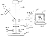
2−3)電子光学系
2−3−1)概要
2−3−2)構成の詳細
2−3−2―1)電子銃(電子線源)
2−3−2−2)一次光学系
2−3−2−3)二次光学系
2−3−3)E×Bユニット(ウィーンフィルタ)
2−3−4)検出器
2−3−5)電源
2−4)プレチャージユニット
2−5)真空排気系
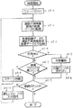
2−6)制御系
2−6−1)構成及び機能
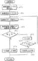
2−6−2)アライメント手順
2−6−3)欠陥検査
2−6−4)制御系構成
2−6−5)ユーザーインターフェース構成
2−7)その他の機能と構成の説明
2−7−1)制御電極
2−7−2)電位印加方法
2−7−3)電子ビームキャリブレーション方法
2−7−4)電極の清掃
2−7−5)アライメント制御方法
2−7−6)EO補正
2−7−7)画像比較方法
2−7−8)デバイス製造方法
2−7−9)検査
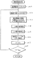
2−8)検査方法
2−8−1)概要
2−8−2)検査アルゴリズム
2−8―2−1)アレイ検査
2−8−2―2)ランダム検査
2−8−2−3)フォーカスマッピング
2−8−2−4)リソマージン測定
3. 他の実施の形態
3−1)ステージ装置の変形例
3−2)電子線装置の他の実施の形態
3−2−1)電子銃(電子線源)
3−2−2)電極の構造
3−3)制振装置に関する実施の形態
3−4)ウェーハの保持に関する実施の形態
3−5)E×B分離器の実施の形態
3−6)製造ラインの実施の形態
3−7)他の電子を用いた実施の形態
3−8)二次電子と反射電子を用いる実施の形態。
Hereinafter, embodiments of a semiconductor inspection apparatus according to the present invention will be described in detail in the following order with reference to the drawings.
2-3-2-2) Primary optical system 2-3-2-3) Secondary optical system 2-3-3) ExB unit (Wien filter)
2-3-4) Detector 2-3-5) Power supply 2-4) Precharge unit 2-5) Evacuation system 2-6) Control system 2-6-1) Configuration and function 2-6-2) Alignment procedure 2-6-3) Defect inspection 2-6-4) Control system configuration 2-6-5) User interface configuration 2-7) Description of other functions and configurations 2-7-1) Control electrode 2-7 -2) Potential application method 2-7-3) Electron beam calibration method 2-7-4) Electrode cleaning 2-7-5) Alignment control method 2-7-6) EO correction 2-7-7) Image Comparison method 2-7-8) Device manufacturing method 2-7-9) Inspection 2-8) Inspection method 2-8-1) Outline 2-8-2) Inspection algorithm 2-8-2-1) Array inspection 2 -8-2-2) Random inspection 2-8-2-3) Focus mapping 2-8- -4)
3-2-2) Structure of electrode 3-3) Embodiment of vibration damping device 3-4) Embodiment of holding wafer 3-5) Embodiment of E × B separator 3-6) Manufacturing line Embodiment 3-7) Embodiment using other electrons 3-8) Embodiment using secondary electrons and reflected electrons.
1 全体構成
まず、該半導体検査装置の全体の構成について説明する。
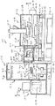
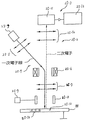
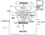
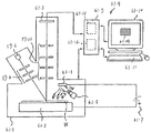
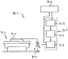
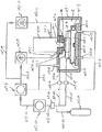
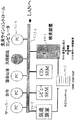
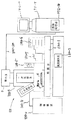
装置の全体構成を図1を用いて述べる。装置は検査装置本体、電源ラック、制御ラック、画像処理ユニット、成膜装置、エッチング装置等から構成される。ドライポンプ等の粗引きポンプはクリーンルームの外に置かれる。検査装置本体内部の主要部分は、図2に示すように、電子ビーム光学鏡筒、真空搬送系、ステージを収容している主ハウジング、除振台、ターボ分子ポンプ等から構成されている。
1. Overall Configuration First, the overall configuration of the semiconductor inspection apparatus will be described.
The overall configuration of the apparatus will be described with reference to FIG. The apparatus includes an inspection apparatus main body, a power supply rack, a control rack, an image processing unit, a film forming apparatus, an etching apparatus, and the like. A roughing pump such as a dry pump is placed outside the clean room. As shown in FIG. 2, the main part inside the inspection apparatus main body is composed of an electron beam optical column, a vacuum transfer system, a main housing containing a stage, a vibration isolation table, a turbo molecular pump, and the like.
制御系には二台のCRTを備え、指示命令入力機能(キーボード等)を備えている。図3は機能からみた構成を示す。電子ビーム鏡筒は主に電子光学系、検出系、光学顕微鏡等から構成されている。電子光学系は電子銃、レンズ等、搬送系は真空搬送ロボット、大気搬送ロボット、カセットローダ、各種位置センサ等から構成されている。 The control system includes two CRTs and an instruction command input function (keyboard or the like). FIG. 3 shows the configuration in terms of functions. The electron beam column mainly includes an electron optical system, a detection system, an optical microscope, and the like. The electron optical system includes an electron gun, a lens, and the like, and the transfer system includes a vacuum transfer robot, an atmospheric transfer robot, a cassette loader, various position sensors, and the like.
ここでは、成膜装置及びエッチング装置、洗浄装置(図示していない)を検査装置本体近くに並べて設置しているが、これらは検査装置本体に組み込んでも良い。これらは、例えば試料の帯電抑制のために又は試料表面のクリーニングに使用される。スパッタ方式を用いると、一台で制膜及びエッチングの両方の機能を持たせることができる。 Here, the film forming apparatus, the etching apparatus, and the cleaning apparatus (not shown) are arranged side by side near the main body of the inspection apparatus, but they may be incorporated in the main body of the inspection apparatus. These are used, for example, for suppressing charging of the sample or for cleaning the surface of the sample. When a sputtering method is used, a single device can have both functions of film control and etching.
図示していないが、使用用途によってはその関連装置を検査装置本体近くに並べて設置するか、それらの関連装置を検査装置本体に組み込んで使用しても良い。或いは、それらの関連装置に検査装置を組み込んでもよい。例えば、化学的機械研磨装置(CMP)と洗浄装置を検査装置本体に組み込んでも良く、或いは、CVD(化学蒸着法:chemical vapor deposition)装置を検査装置に組み込んでもよく、この場合、設置面積や試料搬送のためのユニットの数を節約でき、搬送時間を短縮できるなどのメリットが得られる。 Although not shown, depending on the intended use, the related devices may be arranged side by side near the main body of the inspection apparatus, or the relevant apparatuses may be incorporated in the main body of the inspection apparatus. Alternatively, an inspection device may be incorporated in those related devices. For example, a chemical mechanical polishing apparatus (CMP) and a cleaning apparatus may be incorporated in the inspection apparatus main body, or a CVD (chemical vapor deposition) apparatus may be incorporated in the inspection apparatus. Advantages such as saving the number of units for transport and shortening the transport time can be obtained.
同様に、メッキ装置等の成膜装置に検査装置本体に組み込んでも良い。同様にリソグラフィ装置と組み合わせて使用することも可能である。 Similarly, it may be incorporated in the main body of the inspection apparatus in a film forming apparatus such as a plating apparatus. Similarly, it can be used in combination with a lithographic apparatus.
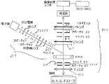
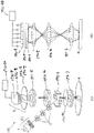
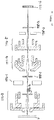
1―1)メインチャンバ、ステージ、真空搬送系外装
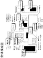
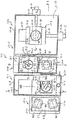
図4、図5、図6において、半導体検査装置の検査部の主要構成要素が示されている。半導体検査装置の検査部は、外部環境からの振動を遮断するためのアクティブ除振台4・1と、検査室であるメインチャンバ4・2と、メインチャンバ上部に設置された電子光学装置4・3と、メインチャンバ内部に搭載されたウェーハスキャン用のXYステージ5・1と、XYステージ動作制御用のレーザ干渉測定系5・2と、メインチャンバに付随する真空搬送系4・4を備え、それらは図4、図5に示されるような位置関係で配置されている。半導体検査装置の検査部は、更に、検査ユニットの環境制御、及びメンテナンスを可能とするための外装6・1を備えており、図6に示されるような位置関係で配置されている。
1-1) Main Chamber, Stage, Exterior of Vacuum Transfer System FIGS. 4, 5, and 6 show main components of an inspection section of a semiconductor inspection apparatus. The inspection section of the semiconductor inspection apparatus includes an active vibration isolation table 4.1 for isolating vibration from the external environment, a main chamber 4.2 serving as an inspection room, and an electron
1−1−1)アクティブ除振台
アクティブ除振台4・1は、アクティブ除振ユニット5・3上に溶接定盤5・4が搭載されており、この溶接定盤上に検査室であるメインチャンバ4・2、メインチャンバ上部に設置された電子光学装置4・3、及びメインチャンバに付随する真空搬送系4・4等を保持するようになっている。これにより、検査部における外部環境からの振動を抑制できるようになっている。この実施の形態では、固有周波数がX方向5Hz、Y方向5Hz、Z方向7.6Hzに対して±25%以内に収まっており、制御性能は、各軸の伝達特性において、1Hzで0dB以下、7.6Hzで−6.4dB以下、10Hzで−8.6dB以下、20Hzで−17.9dB以下となっている(以上、定盤上無負荷状態)。アクティブ除振台の他の構造では、メインチャンバ、電子光学装置等を吊り下げて保持するようになっている。さらに他の構造では、石定盤を搭載し、メインチャンバ等を保持するようになっている。
1-1-1) Active anti-vibration table The active anti-vibration table 4.1 has a welding surface plate 5.4 mounted on the active vibration isolation unit 5.3 and an inspection room on the welding surface plate. The main chambers 4.2, the electron optical devices 4.3 provided above the main chamber, and the vacuum transfer systems 4.4 associated with the main chamber are held. This makes it possible to suppress vibration from the external environment in the inspection unit. In this embodiment, the natural frequency is within ± 25% with respect to 5 Hz in the X direction, 5 Hz in the Y direction, and 7.6 Hz in the Z direction, and the control performance is 0 dB or less at 1 Hz in the transmission characteristics of each axis. It is -6.4 dB or less at 7.6 Hz, -8.6 dB or less at 10 Hz, and -17.9 dB or less at 20 Hz (there is no load on the surface plate). In another structure of the active vibration isolation table, the main chamber, the electron optical device, and the like are suspended and held. In still another structure, a stone platen is mounted to hold a main chamber and the like.
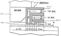
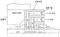
1−1−2)メインチャンバ
メインチャンバ4・2は、検査環境である真空度(10−4Pa以下)を実現するためにターボ分子ポンプ7・2を下部に直接保持しており、ウェーハスキャン用の高精度のXYステージ5・1を内部に備え、外部からの磁気を遮蔽できるようになっている。この実施の形態では、高精度XYステージの設置面の平面度を可能な限り良くするために以下の構造となっている。メインチャンバの下板7・3は、溶接定盤上に用意された特に平面度のよい部分7・4(この実施の形態では、平面度5μm以下)に設置、固定されている。さらに、メインチャンバ内部にはステージ設置面として中板を設けている。中板は、メインチャンバの下板に対して3点で支持されており、下板の平面度の影響を直接受けないようになっている。この実施の形態では、支持部分が球面座7・6により構成されている。中板は、自重及びステージ重さを負荷された場合にステージ設置面を平面度5μm以下に達成できるようになっている。また、内部の圧力変化(大気圧より真空度10−4Pa以下)によるメインチャンバ変形のステージ取付け面に対する影響を抑えるために、下板の中板3点支持部分付近は、溶接定盤に直接固定されている。
1-1-2) Main Chamber The main chambers 4.2 directly hold turbo molecular pumps 7.2 at the lower part to realize a vacuum degree (10 −4 Pa or less) as an inspection environment, and perform wafer scanning. High precision XY stage 5.1 is provided inside to shield external magnetism. In this embodiment, the following structure is used to improve the flatness of the installation surface of the high-precision XY stage as much as possible. The lower plate 7.3 of the main chamber is installed and fixed to a portion 7.4 (particularly 5 μm or less in this embodiment) having particularly good flatness prepared on the welding platen. Further, a middle plate is provided inside the main chamber as a stage installation surface. The middle plate is supported at three points with respect to the lower plate of the main chamber, and is not directly affected by the flatness of the lower plate. In this embodiment, the support portion is constituted by
XYステージを高精度に制御するためにレーザ干渉計によるステージ位置の測定系が設置されている。干渉計8・1は、測定誤差を抑えるために真空中に配されおり、直接測定誤差となる干渉計自体の振動を限りなくゼロとするために、この実施の形態では剛性の高いチャンバ壁7・7に直接固定されている。また、測定位置と検査位置の誤差を無くすために、干渉計による測定部分の延長線上が検査部分と極力一致するようになっている。また、ステージのXY動作を行なうためのモータ8・2はこの実施の形態ではチャンバ壁7・7により保持されているが、メインチャンバへ及ぼすモータ振動の影響をさらに抑制する必要がある場合には溶接定盤7・1により直接保持し、ベローズ等の振動を伝達しない構造によりメインチャンバに取付けられる。 In order to control the XY stage with high accuracy, a stage position measurement system using a laser interferometer is provided. The interferometer 8.1 is arranged in a vacuum in order to suppress a measurement error, and in order to minimize the vibration of the interferometer itself, which directly causes a measurement error, to zero as much as possible.・ It is directly fixed to 7. Further, in order to eliminate an error between the measurement position and the inspection position, the extension of the measurement portion by the interferometer is made to coincide with the inspection portion as much as possible. Although the motors 8.2 for performing the XY operation of the stage are held by the chamber walls 7.7 in this embodiment, if it is necessary to further suppress the influence of the motor vibration on the main chamber, It is directly held by the welding platens 7.1 and is attached to the main chamber by a structure that does not transmit vibration such as bellows.
メインチャンバ4・2は、検査部分に及ぼす外部磁場の影響を遮断するために透磁率の高い材料で構成されている。この実施の形態では、パーマロイとSS400等の鉄に防錆コーティングとしてNiめっきを施したものとなっている。他の実施の形態では、パーメンジェール、スーパーマロイ、電磁軟鉄、純鉄などとなっている。さらに、チャンバ内部の検査部周辺を直接透磁率の高い材料で覆うことも磁気遮蔽効果として有効である。
The
1−1−3)XYステージ
XYステージ5・1は、真空中でウェーハを高精度にスキャンできるようになっている。XおよびYのストロークは、例えば200mmウェーハ用としてそれぞれ200mm〜300mm、300mmウェーハ用としてそれぞれ300mm〜600mmとなっている。この実施の形態でのXYステージの駆動は、メインチャンバ壁に固定されたXおよびY軸駆動用のモータ8・2と、これらに磁性流体シール8・3を介して取付けられたボールネジ8・5により行われる。XおよびY駆動用のボールネジが、チャンバ壁に対して固定された状態でXY動作を行なえるために、この実施の形態ではステージ構造は、以下のようになっている。
1-1-3) XY Stage The XY stage 5.1 can scan a wafer with high accuracy in a vacuum. The X and Y strokes are, for example, 200 mm to 300 mm for a 200 mm wafer, and 300 mm to 600 mm, respectively, for a 300 mm wafer. In this embodiment, the XY stage is driven by motors 8.2 for driving the X and Y axes fixed to the wall of the main chamber, and ball screws 8.5 attached to these via magnetic fluid seals 8.3. Is performed by In this embodiment, the stage structure is as follows in order to perform the XY operation with the X and Y drive ball screws fixed to the chamber wall.
まず下段には、Yステージ7・10が配されており、駆動のためのボールネジ7・8およびクロスローラーガイド7・11が設置されている。Yステージ上部には、X軸駆動用のボールネジ7・14が設置された中間ステージ7・12を介してさらにその上部にXステージ7・13が搭載されている。中間ステージとYステージおよびXステージは、Y軸方向にクロスローラーガイドにより連結されている。これにより、Y軸移動時にはYステージおよび連結部7・14によりXステージが移動し、中間ステージは固定された状態のままとなる。他の実施の形態では、中間ステージは上段軸と並べて配置される二段構造となっている。また、他の実施の形態のXYステージでは、XYステージそのものがリニアモータで駆動されるようになっている。さらに、全ストロークに渡りレーザ干渉計による測定が可能なように高精度ミラー8・4(この実施の形態では、平面度λ/20以下、材質は合成石英にアルミ蒸着)が設置されている。 First, Y stages 7 and 10 are arranged in the lower stage, and ball screws 7.8 and cross roller guides 7 and 11 for driving are installed. On the upper part of the Y stage, an X stage 713 is mounted further above an intermediate stage 712 provided with ball screws 714 for driving the X axis. The intermediate stage, the Y stage, and the X stage are connected by a cross roller guide in the Y axis direction. As a result, during the movement of the Y axis, the X stage is moved by the Y stage and the connecting portions 7-14, and the intermediate stage remains fixed. In another embodiment, the intermediate stage has a two-stage structure arranged side by side with the upper shaft. In the XY stage according to another embodiment, the XY stage itself is driven by a linear motor. Furthermore, high-precision mirrors 8.4 (in this embodiment, a flatness of λ / 20 or less, and the material is aluminum deposited on synthetic quartz) are provided so that measurement by a laser interferometer can be performed over the entire stroke.
また、真空中でウェーハアライメントを行なうためにXYステージ上にはθステージ7・15が設置されている。この実施の形態におけるθステージでは、駆動用として2つの超音波モータ、位置制御用としてリニアスケールが配されている。X、Y及びθ動作を行なう可動部に接続された種々のケーブルは、XステージおよびYステージにそれぞれ保持されたケーブルベアによりクランプされ、チャンバ壁に設置されたフィードスルーを介してメインチャンバ外部へと接続されている。 In order to perform wafer alignment in a vacuum, .theta. Stages 7.15 are provided on the XY stage. In the θ stage in this embodiment, two ultrasonic motors are provided for driving, and a linear scale is provided for position control. Various cables connected to the movable parts performing the X, Y, and θ operations are clamped by cable bearers held on the X stage and the Y stage, respectively, to the outside of the main chamber via feedthroughs installed on the chamber walls. Is connected to
上記の構造による本実施の形態のスペックを表1、表2に示す。 Tables 1 and 2 show the specifications of the present embodiment having the above structure.

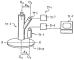
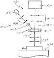
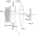
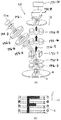
1−2)レーザ干渉測定系
レーザ干渉測定系は、X軸およびY軸に平行で、その延長線上が検査位置に相当する光軸を有するレーザ光学系と、その間に配された干渉計8・1により構成されている。本実施の形態における光学系の配置は、図9、図10に示されるような位置関係で配置されている。溶接定盤上に設置されたレーザ9・1より発射されたレーザ光は、ベンダ9・2により垂直に立ち上げられたのちにベンダ10・1により測定面と平行に曲げられる。さらに、スプリッタ9・4によりX軸測定用とY軸測定用に分配された後に、ベンダ10・3およびベンダ9・6によりそれぞれY軸およびX軸に平行に曲げられ、メインチャンバ内部へと導入される。
1-2) Laser Interferometer The laser interferometer is a laser optical system having an optical axis parallel to the X-axis and the Y-axis, the extension of which is equivalent to the inspection position, and an
上記光学系の立上げ時の調整方法を以下に説明する。まず、レーザより発射されたレーザ光が、ベンダ9・2により垂直に、ベンダ10・1により水平に曲げられるように調整する。その後、ベンダ10・3により曲げられ、Y軸に対して高精度に垂直に設置されたミラー8・4に反射して戻る光軸が入射の光軸に完全に一致するようにベンダ10・3を調整する。光軸の確認を、反射光を妨げないように干渉計を外した状態で、レーザ直後で行なうことにより、精度の高い調整が可能となる。また、X軸の光軸調整は、Y軸の光軸調整を行なった後に、スプリッタ9・4とベンダ9・6により独立に行なうことができる。調整の要領はY軸と同様である。さらに、X軸およびY軸の入射光と反射光の軸を調整した後に、各光軸の交点(ミラーがないと考えた場合)をウェーハ検査位置に一致させる必要がある。このために、ベンダ10・3を固定しているブラケットはY軸に対して垂直に、ベンダ9・6を固定しているブラケットはX軸に対して垂直に入射光と反射光を一致させたまま移動できるようになっている。さらに、ベンダ10・1、スプリッタ9・4、ベンダ10・3、ベンダ9・6はそれぞれの位置関係を保持したまま上下に移動できることが望ましい。 An adjustment method at the time of starting the optical system will be described below. First, the laser beam emitted from the laser is adjusted so as to be bent vertically by the benders 9.2 and horizontally by the benders 10.1. Thereafter, the vendor 10.3 is bent by the vendor 10.3 so that the optical axis reflected by the mirror 8.4, which is installed vertically with high precision with respect to the Y-axis, returns completely to the incident optical axis. To adjust. By checking the optical axis immediately after the laser with the interferometer removed so as not to interfere with the reflected light, highly accurate adjustment is possible. Further, the optical axis adjustment of the X axis can be performed independently by the splitters 9.4 and the vendors 9.6 after the optical axis adjustment of the Y axis is performed. The adjustment procedure is the same as that for the Y axis. Furthermore, after adjusting the axes of the incident light and the reflected light on the X axis and the Y axis, it is necessary to match the intersection of each optical axis (when there is no mirror) with the wafer inspection position. For this reason, the bracket fixing the benders 10.3 and the brackets fixing the benders 9.6 and incident light and reflected light perpendicular to the Y axis, respectively. You can move as it is. Further, it is desirable that the bender 10.1, the splitter 9.4, the bender 10.3, and the bender 9.6 can be moved up and down while maintaining their respective positional relationships.
また、立上げ後、運転中の本装置におけるレーザの交換に伴う光軸調整方法を以下に説明する。運転中のメインチャンバ内部が真空に保持されている状態の装置では、干渉計を取り外した光軸等が困難となっている。そこで、メインチャンバ外部の光路に数箇所ターゲット10・2を設置し、立上げ時の光路がメインチャンバ外部のみで判断できる治具が用意されている。レーザ交換後は、レーザ取付け台に備えられた調整機能のみでターゲット10・2に対して光軸を調整することにより、立上げ時に行なった調整を再現できるようになっている。 In addition, a method of adjusting an optical axis accompanying laser replacement in the apparatus during operation after startup will be described below. In an apparatus in which the inside of the main chamber during operation is kept in a vacuum, it is difficult to form an optical axis from which the interferometer is removed. Therefore, a jig is provided in which several targets 10.2 are installed in the optical path outside the main chamber and the optical path at startup can be determined only outside the main chamber. After the laser replacement, the adjustment performed at the time of start-up can be reproduced by adjusting the optical axis with respect to the target 10.2 only by the adjustment function provided on the laser mounting table.
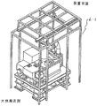
1−3)検査部外装
検査部外装4・7は、メンテナンス用のフレーム構造としての機能を備えられるようになっている。本実施の形態では、収納可能な両持ちクレーン11・1が上部に搭載されている。クレーン11・1は横行レール11・2に取付けられ、横行レールはさらに走行レール(縦)11・3に設置されている。走行レールは、通常時には図11のように収納状態となっているのに対して、メンテナンス時には図12のように上昇し、クレーンの上下方向のストロークを大きくすることが可能となっている。これにより、メンテナンス時には外装に内蔵されたクレーンにより電子光学装置4・3、メインチャンバ天板、XYステージ5・1を装置背面に脱着可能となっている。外装に内蔵されたクレーンの他の実施の形態では、回転可能な片持ち軸を持つクレーン構造となっている。
1-3) Inspection Unit Exterior The
また、検査部外装は、環境チャンバとしての機能を兼ね備えることも可能となっている。これは、必要に応じて温度、湿度管理とともに、磁気遮蔽効果を有するようになっている。 Further, the inspection unit exterior can also have a function as an environmental chamber. This has a magnetic shielding effect as well as temperature and humidity management as needed.
2 実施の形態
以下、図面を参照して、本発明の好ましい実施の形態について、検査対象として表面にパターンが形成された基板すなわちウェーハを検査する半導体検査装置として説明する。
2. Embodiment Hereinafter, a preferred embodiment of the present invention will be described with reference to the drawings as a semiconductor inspection apparatus for inspecting a substrate having a pattern formed on a surface, that is, a wafer, as an inspection target.
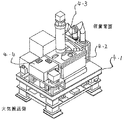
2−1)搬送系
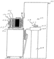
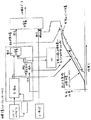
図13及び図14は、本発明に係る半導体検査装置の主要構成要素を立面図及び平面図で示している。この半導体検査装置13・1は、複数枚のウェーハを収納したカセットを保持するカセットホルダ13・2と、ミニエンバイロメント装置13・3と、ワーキングチャンバを構成するローダハウジング13・5と、ウェーハをカセットホルダ13・2から主ハウジング13・4内に配置されたステージ装置13・6上に装填するローダー13・7と、真空ハウジングに取り付けられた電子光学装置13・8とを備え、それらは図13及び図14に示されるような位置関係で配置されている。
2-1) Transport System FIGS. 13 and 14 show main components of the semiconductor inspection apparatus according to the present invention in elevation and plan views. The semiconductor inspection device 13.1 includes a cassette holder 13.2 for holding a cassette containing a plurality of wafers, a mini-environment device 13.3, a loader housing 13.5 for forming a working chamber, and a wafer. A loader 13.7 is loaded from a cassette holder 13.2 onto a stage device 13.6 arranged in a main housing 13.4, and an electro-optical device 13.8 mounted on a vacuum housing. 13 and 14 are arranged in a positional relationship as shown in FIG.
半導体検査装置13・1は、更に、真空の主ハウジング13・4内に配置されたプレチャージユニット13・9と、ウェーハに電位を印加する電位印加機構と、電子ビームキャリブレーション機構と、ステージ装置上でのウェーハの位置決めを行うためのアライメント制御装置13・10を構成する光学顕微鏡13・11とを備えている。
The semiconductor inspection apparatus 13.1 further includes a precharge unit 13.9 arranged in a vacuum main housing 13.4, a potential application mechanism for applying a potential to the wafer, an electron beam calibration mechanism, and a stage device.
2−1−1)カセットホルダ
カセットホルダ13・2は、複数枚(例えば25枚)のウェーハが上下方向に平行に並べられた状態で収納されたカセット13・12(例えば、アシスト社製のSMIF、FOUPのようなクローズドカセット)を複数個(この実施の形態では2個)保持するようになっている。このカセットホルダ13・2としては、カセットをロボット等により搬送してきて自動的にカセットホルダ13・2に装填する場合にはそれに適した構造のものを、また人手により装填する場合にはそれに適したオープンカセット構造のものをそれぞれ任意に選択して設置できるようになっている。カセットホルダ13・2は、この実施の形態では、自動的にカセット13・12が装填される形式であり、例えば昇降テーブル13・13と、その昇降テーブル13・13を上下移動させる昇降機構13・14とを備え、カセット13・12は昇降テーブル13・13上に図14で鎖線で示す状態で自動的にセット可能にされ、セット後、図14で実線で示す状態に自動的に回転されてミニエンバイロメント装置内の第1の搬送ユニットの回動軸線に向けられる。
2-1-1) Cassette holder The
また、昇降テーブル13・13は図13で鎖線で示す状態に降下される。このように、自動的に装填する場合に使用するカセットホルダ或いは人手により装填する場合に使用するカセットホルダはいずれも公知の構造のものを適宜使用すれば良いので、その構造及び機能の詳細な説明は省略する。 Further, the lifting tables 13 are lowered to the state shown by the chain line in FIG. As described above, the cassette holder used for automatic loading or the cassette holder used for manual loading may be of a known structure as appropriate, and a detailed description of the structure and functions thereof will be given. Is omitted.
別の実施の形態では、図15に示すように、複数の300mm基板を箱本体15・1の内側に固定した溝型ポケット(記載せず)に収納した状態で収容し、搬送、保管等を行うものである。この基板搬送箱15・2は、角筒状の箱本体15・1と基板搬出入ドア自動開閉装置に連絡されて箱本体15・1の側面の開口部を機械により開閉可能な基板搬出入ドア15・3と、開口部と反対側に位置し、フィルタ類およびファンモータの着脱を行うための開口部を覆う蓋体15・4と、基板W(図13)を保持するための溝型ポケット(図示せず)、ULPAフィルタ15・5、ケミカルフィルタ15・6、ファンモータ15・7とから構成されている。この実施の態様では、ローダー13・7のロボット式の第1の搬送ユニット15・7により、基板を出し入れする。 In another embodiment, as shown in FIG. 15, a plurality of 300 mm substrates are accommodated in a groove-type pocket (not shown) fixed inside the box body 15.1, and transport, storage, etc. are performed. Is what you do. The substrate transport box 15.2 is connected to a rectangular cylindrical box body 15.1 and a substrate loading / unloading door automatic opening / closing device to open and close a side opening of the box body 15.1 mechanically. 15.3, a cover 15.4 located on the opposite side of the opening to cover the opening for attaching and detaching the filters and the fan motor, and a grooved pocket for holding the substrate W (FIG. 13). (Not shown), an ULPA filter 15.5, a chemical filter 15.6, and a fan motor 15.7. In this embodiment, the substrate is loaded and unloaded by the robotic first transfer units 15.7 of the loaders 13.7.
なお、カセット13・12内に収納される基板すなわちウェーハは、検査を受けるウェーハであり、そのような検査は、半導体製造工程中でウェーハを処理するプロセスの後、若しくはプロセスの途中で行われる。具体的には、成膜工程、CMP、イオン注入等を受けた基板すなわちウェーハ、表面に配線パターンが形成されたウェーハ、又は配線パターンが未だに形成されていないウェーハが、カセット内に収納される。カセット12・12内に収容されるウェーハは多数枚上下方向に隔ててかつ平行に並べて配置されているため、任意の位置のウェーハと後述する第1の搬送ユニットで保持できるように、第1の搬送ユニットのアームを上下移動できるようになっている。また、カセットにはプロセス後のウェーハ表面の酸化等の防止のために、カセット内の水分をコントロールするための機能が設けられている。例えば、シリカゲル等の除湿剤がカセットの中に置かれている。この場合、除湿効果があれば、任意のものを利用することができる。
The substrates or wafers housed in the
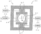
2−1−2)ミニエンバイロメント装置
図13〜図16において、ミニエンバイロメント装置13・3は、雰囲気制御されるようになっているミニエンバイロメント空間16・1を構成するハウジング16・2と、ミニエンバイロメント空間16・1内で清浄空気のような気体を循環して雰囲気制御するための気体循環装置16・3と、ミニエンバイロメント空間16・1内に供給された空気の一部を回収して排出する排出装置16・4と、ミニエンバイロメント空間16・1内に配設されていて検査対象としての基板すなわちウェーハを粗位置決めするプリアライナー16・5とを備えている。
2-1-2) Mini-environment device In FIGS. 13 to 16, a mini-environment device 13.3 includes a housing 16-2 that forms a mini-environment space 16.1. A gas circulating device 16.3 for circulating gas such as clean air in the mini-environment space 16.1 to control the atmosphere, and a part of the air supplied to the mini-environment space 16.1. The apparatus includes a discharge device 16.4 for collecting and discharging, and a pre-aligner 16.5 arranged in the mini-environment space 16.1 for roughly positioning a substrate, that is, a wafer to be inspected.
ハウジング16・2は、頂壁16・6、底壁16・7及び四周を囲む周壁16・8を有しており、ミニエンバイロメント空間16・1を外部から遮断する構造になっている。ミニエンバイロメント空間16・1を雰囲気制御するために、気体循環装置16・3は、図16に示されるように、ミニエンバイロメント空間16・1内において、頂壁16・6に取り付けられていて、気体(この実施の形態では空気)を清浄にして一つ又はそれ以上の気体吹き出し口(図示せず)を通して清浄空気を真下に向かって層流状に流す気体供給ユニット16・9と、ミニエンバイロメント空間16・1内において底壁16・7の上に配置されていて、底に向かって流れ下った空気を回収する回収ダクト16・10と、回収ダクト16・10と気体供給ユニット16・9とを接続して回収された空気を気体供給ユニット16・9に戻す導管16・11とを備えている。
The housing 16.2 has a top wall 16.6, a bottom wall 16.7, and a peripheral wall 16.8 surrounding four circumferences, and has a structure in which the mini-environment space 16.1. In order to control the atmosphere of the mini-environment space 16.1, the gas circulation device 16.3 is mounted on the top wall 16.6 in the mini-environment space 16.1 as shown in FIG. A gas supply unit 16.9, which cleans a gas (air in this embodiment) and causes the clean air to flow in a laminar flow immediately below through one or more gas outlets (not shown); A collection duct 16.10 disposed on the bottom wall 16.7 in the environment space 16.1 for collecting air flowing down to the bottom; a collection duct 16.10. 9 and a
この実施の形態では、気体供給ユニット16・9は供給する空気の約20%をハウジング16・2の外部から取り入れて清浄にするようになっているが、この外部から取り入れられる気体の割合は任意に選択可能である。気体供給ユニット16・9は、清浄空気を作りだすための公知の構造のHEPA若しくはULPAフィルタを備えている。清浄空気の層流状の下方向の流れすなわちダウンフローは、主に、ミニエンバイロメント空間16・1内に配置された後述する第1の搬送ユニットによる搬送面を通して流れるように供給され、搬送ユニットにより発生する虞のある塵埃がウェーハに付着するのを防止するようになっている。したがって、ダウンフローの噴出口は必ずしも図示のように頂壁に近い位置である必要はなく、搬送ユニットによる搬送面より上側にあればよい。また、ミニエンバイロメント空間16・1全面に亘って流す必要もない。
In this embodiment, the gas supply unit 16.9 takes in about 20% of the supplied air from the outside of the housing 16.2 and cleans it, but the ratio of the gas taken in from the outside is arbitrary. Can be selected. The gas supply units 16.9 are provided with HEPA or ULPA filters of a known structure for producing clean air. The laminar downward flow of the clean air, that is, the downflow, is mainly supplied so as to flow through a transfer surface of a first transfer unit described later disposed in the
なお、場合によっては、清浄空気としてイオン風を使用することによって清浄度を確保することができる。また、ミニエンバイロメント空間16・1内には清浄度を観察するためのセンサを設け、清浄度が悪化したときに装置をシャットダウンすることもできる。 In some cases, cleanliness can be ensured by using ion wind as clean air. Further, a sensor for observing cleanliness can be provided in the mini-environment space 16.1, and the apparatus can be shut down when the cleanliness deteriorates.
ハウジング16・2の周壁16・8のうちカセットホルダ13・2に隣接する部分には出入り口13・15が形成されている。出入り口13・15近傍には公知の構造のシャッタ装置を設けて出入り口13・15をミニエンバイロメント装置側から閉じるようにしてもよい。ウェーハ近傍でつくる層流のダウンフローは、例えば0.3ないし0.4m/secの流速でよい。気体供給ユニット16・9はミニエンバイロメント空間16・1内でなくその外側に設けてもよい。
排出装置16・4は、前記搬送ユニットのウェーハ搬送面より下側の位置で搬送ユニットの下部に配置された吸入ダクト16・12と、ハウジング16・2の外側に配置されたブロワー16・13と、吸入ダクト16・12とブロワー16・13とを接続する導管16・14とを備えている。この排出装置16・4は、搬送ユニットの周囲を流れ下り搬送ユニットにより発生する可能性のある塵埃を含んだ気体を、吸入ダクト16・12により吸引し、導管16・14及びブロワー16・13を介してハウジング16・2の外側に排出する。この場合、ハウジング16・2の近くに引かれた排気管(図示せず)内に排出してもよい。
The discharge device 16.4 includes a suction duct 16.12 disposed below the transfer unit at a position below the wafer transfer surface of the transfer unit, and a blower 16.13 disposed outside the housing 16.2. , And
ミニエンバイロメント空間16・1内に配置されたプリアライナー16・5は、ウェーハに形成されたオリエンテーションフラット(円形のウェーハの外周に形成された平坦部分を言い、以下においてオリフラと呼ぶ)や、ウェーハの外周縁に形成された一つ又はそれ以上のV型の切欠きすなわちノッチを光学的に或いは機械的に検出してウェーハの軸線O−Oの周りの回転方向の位置を約±1度の精度で予め位置決めしておくようになっている。プリアライナー16・5は検査対象の座標を決める機構の一部を構成し、検査対象の粗位置決めを担当する。このプリアライナー16・5自体は公知の構造のものでよいので、その構造、動作の説明は省略する。 The pre-aligner 16.5 disposed in the mini-environment space 16.1 is provided with an orientation flat (referred to as a flat portion formed on the outer periphery of a circular wafer, hereinafter referred to as an orientation flat) formed on the wafer or a wafer. One or more V-shaped notches or notches formed in the outer peripheral edge of the wafer are optically or mechanically detected so that the position in the rotational direction about the axis OO of the wafer is about ± 1 degree. Positioning is performed in advance with precision. The pre-aligner 16.5 constitutes a part of a mechanism for determining coordinates of the inspection target, and is responsible for coarse positioning of the inspection target. Since the pre-aligners 16 and 5 themselves may have a known structure, the description of the structure and operation will be omitted.
なお、図示しないが、プリアライナー16・5の下部にも排出装置用の回収ダクトを設けて、プリアライナー16・5から排出された塵埃を含んだ空気を外部に排出するようにしてもよい。 Although not shown, a collection duct for a discharging device may be provided below the pre-aligner 16.5 to discharge the air containing dust discharged from the pre-aligner 16.5 to the outside.
2−1−3)主ハウジング
図13〜図15において、ワーキングチャンバ13・16を構成する主ハウジング13・4は、ハウジング本体13・17を備え、そのハウジング本体13・17は、台フレーム13・18上に配置された振動遮断装置すなわち防振装置13・19の上に載せられたハウジング支持装置13・20によって支持されている。ハウジング支持装置13・20は矩形に組まれたフレーム構造体13・21を備えている。ハウジング本体13・17はフレーム構造体13・21上に配設固定されていて、フレーム構造体上に載せられた底壁13・22と、頂壁13・23と、底壁13・22及び頂壁13・23に接続されて四周を囲む周壁13・24とを備えていてワーキングチャンバ13・16を外部から隔離している。底壁13・22は、この実施の形態では、上に載置されるステージ装置等の機器による加重で歪みの発生しないように比較的肉厚の厚い鋼板で構成されているが、その他の構造にしてもよい。
2-1-3) Main Housing In FIGS. 13 to 15, the
この実施の形態において、ハウジング本体及びハウジング支持装置13・20は、剛構造に組み立てられていて、台フレーム13・18が設置されている床からの振動がこの剛構造に伝達されるのを防振装置13・19で阻止するようになっている。ハウジング本体13・17の周壁13・24のうち後述するローダハウジングに隣接する周壁にはウェーハ出し入れ用の出入り口14・1が形成されている。
In this embodiment, the housing body and the
なお、防振装置13・19は、空気バネ、磁気軸受け等を有するアクティブ式のものでも、或いはこれらを有するパッシブ式のもよい。いずれも公知の構造のものでよいので、それ自体の構造及び機能の説明は省略する。ワーキングチャンバ13・16は公知の構造の真空装置(図示せず)により真空雰囲気に保たれるようになっている。台フレーム13・18の下には装置全体の動作を制御する制御装置2が配置されている。主ハウジングの圧力は通常10−4〜10−6Paに保たれている。
Note that the
2−1−4)ローダハウジング
図13〜図15及び図17において、ローダハウジング13・5は、第1のローディングチャンバ14・2と第2のローディングチャンバ14・3とを構成するハウジング本体14・4を備えている。ハウジング本体14・4は底壁17・1と、頂壁17・2と、四周を囲む周壁17・3と、第1のローディングチャンバ14・2と第2のローディングチャンバ14・3とを仕切る仕切壁14・5とを有していて、両ローディングチャンバを外部から隔離できるようになっている。仕切壁14・5には両ローディングチャンバ間でウェーハのやり取りを行うための開口すなわち出入り口17・4が形成されている。また、周壁17・3のミニエンバイロメント装置及び主ハウジングに隣接した部分には出入り口14・6及び14・7が形成されている。
2-1-4) Loader housing In FIG. 13 to FIG. 15 and FIG. 17, the loader housing 13.5 includes a housing
このローダハウジング13・5のハウジング本体14・4は、ハウジング支持装置13・20のフレーム構造体13・21上に載置されてそれによって支持されている。したがって、このローダハウジング13・5にも床の振動が伝達されないようになっている。ローダハウジング13・5の出入り口14・6とミニエンバイロメント装置13・3のハウジング16・2の出入り口13・25とは整合されていて、そこにはミニエンバイロメント空間16・1と第1のローディングチャンバ14・2との連通を選択的に阻止するシャッタ装置14・8が設けられている。 The housing bodies 14.4 of the loader housings 13.5 are mounted on and supported by the frame structures 13.21 of the housing support devices 13.20. Therefore, vibration of the floor is not transmitted to the loader housings 13.5. The entrance 14.6 of the loader housing 13.5 and the entrance 13.25 of the housing 16.2 of the mini-environment device 13.3 are aligned, where the mini-environment space 16.1 and the first loading are located. A shutter device 14.8 is provided for selectively blocking communication with the chamber 14.2.
シャッタ装置14・8は、出入り口13・25及び14・6の周囲を囲んで側壁17・3と密に接触して固定されたシール材13・26、シール材13・26と共動して出入り口を介しての空気の流通を阻止する扉13・27と、その扉を動かす駆動装置13・28とを有している。また、ローダハウジング13・5の出入り口14・7とハウジング本体13・17の出入り口14・1とは整合されていて、そこには第2のローディングチャンバ14・3とワーキンググチャンバ13・16との連通を選択的に密封阻止するシャッタ装置13・29が設けられている。シャッタ装置13・29は、出入り口14・7及び14・1の周囲を囲んで側壁17・3及び13・24と密に接触してそれらに固定されたシール材13・30、シール材13・30と共動して出入り口を介しての空気の流通を阻止する扉14・9と、その扉を動かす駆動装置13・31とを有している。
The shutter devices 14.8 surround the doors 13.25 and 14.6, and are fixed in close contact with the side walls 17.3. The sealing members 13.26 are cooperated with the sealing members 13.26. And
更に、仕切壁14・5に形成された開口には、扉によりそれを閉じて第1及び第2のローディングチャンバ間の連通を選択的に密封阻止するシャッタ装置14・10が設けられている。これらのシャッタ装置14・8、13・29及び414・10は、閉じ状態にあるとき各チャンバを気密シールできるようになっている。これらのシャッタ装置は公知のものでよいので、その構造及び動作の詳細な説明は省略する。
Further,
なお、ミニエンバイロメント装置13・3のハウジング16・2の支持方法とローダハウジングの支持方法が異なり、ミニエンバイロメント装置13・3を介して床からの振動がローダハウジング13・5及び主ハウジング13・4に伝達されるのを防止するために、ハウジング16・2とローダハウジング13・5との間には出入り口の周囲を気密に囲むように防振用のクッション材を配置しておけば良い。
Note that the method of supporting the housing 16.2 of the mini-environment device 13.3 is different from the method of supporting the loader housing. Vibration from the floor via the mini-environment device 13.3 causes the loader housing 13.5 and the
第1のローディングチャンバ14・2内には、複数(この実施の形態では2枚)のウェーハを上下に隔てて水平の状態で支持するウェーハラック14・11が配設されている。ウェーハラック14・11は、図18に示されるように、矩形の基板18・1の四隅に互いに隔てて直立状態で固定された支柱18・2を備え、各支柱18・2にはそれぞれ2段の支持部18・3及び18・4が形成され、その支持部の上にウェーハWの周縁を載せて保持するようになっている。そして後述する第1及び第2の搬送ユニットのアームの先端を隣接する支柱間からウェーハに接近させてアームによりウェーハを把持するようになっている。
In the first loading chamber 14.2, there are arranged wafer racks 14.11 which support a plurality of (two in this embodiment) wafers vertically separated from each other in a horizontal state. As shown in FIG. 18, the wafer racks 14 and 11 are provided with uprights 18.2. The uprights 18.2. The
ローディングチャンバ14・2及び14・3は、図示しない真空ポンプを含む公知の構造の真空排気装置(図示せず)によって高真空状態(真空度としては10−4〜10−6Pa)に雰囲気制御され得るようになっている。この場合、第1のローディングチャンバ14・2を低真空チャンバとして低真空雰囲気に保ち、第2のローディングチャンバ14・3を高真空チャンバとして高真空雰囲気に保ち、ウェーハの汚染防止を効果的に行うこともできる。このような構造を採用することによってローディングチャンバ内に収容されていて次に欠陥検査されるウェーハをワーキングチャンバ内に遅滞なく搬送することができる。このようなローディングチャンバを採用することによって、後述するマルチビーム型電子装置原理と共に、欠陥検査のスループットを向上させ、更に保管状態が高真空状態であることを要求される電子源周辺の真空度を可能な限り高真空度状態にすることができる。 Atmosphere control of the loading chambers 14-2 and 14-3 to a high vacuum state (a degree of vacuum of 10 -4 to 10 -6 Pa) by a vacuum exhaust device (not shown) having a known structure including a vacuum pump (not shown). That can be done. In this case, the first loading chamber 14.2 is maintained in a low vacuum atmosphere as a low vacuum chamber, and the second loading chamber 14.3 is maintained in a high vacuum atmosphere as a high vacuum chamber, thereby effectively preventing contamination of the wafer. You can also. By adopting such a structure, the wafer accommodated in the loading chamber and subjected to the next defect inspection can be transferred into the working chamber without delay. By employing such a loading chamber, the throughput of defect inspection is improved together with the principle of a multi-beam type electronic device described later, and the degree of vacuum around the electron source, which is required to be kept in a high vacuum state, is further improved. The state of vacuum can be as high as possible.
第1及び第2のローディングチャンバ14・2及び14・3は、それぞれ真空排気配管と不活性ガス(例えば乾燥純窒素)用のベント配管(それぞれ図示せず)が接続されている。これによって、各ローディングチャンバ内の大気圧状態は不活性ガスベント(不活性ガスを注入して不活性ガス以外の酸素ガス等が表面に付着するのを防止する)によって達成される。このような不活性ガスベントを行う装置自体は公知の構造のものでよいので、その詳細な説明は省略する。 The first and second loading chambers 14.2 and 14.3 are respectively connected to a vacuum exhaust pipe and a vent pipe (not shown) for an inert gas (for example, dry pure nitrogen). Thereby, the atmospheric pressure state in each loading chamber is achieved by an inert gas vent (injecting an inert gas to prevent oxygen gas and the like other than the inert gas from adhering to the surface). Since the apparatus itself for performing such inert gas venting may have a known structure, a detailed description thereof will be omitted.
なお、電子線を使用する本発明の検査装置において、後述する電子光学系の電子源として使用される代表的な六硼化ランタン(LaB6)等は一度熱電子を放出する程度まで高温状態に加熱された場合には、酸素等に可能な限り接触させないことがその寿命を縮めないために肝要であるが、電子光学系が配置されているワーキングチャンバにウェーハを搬入する前段階で上記のような雰囲気制御を行うことにより、より確実に実行できる。 In the inspection apparatus of the present invention using an electron beam, a typical lanthanum hexaboride (L a B 6 ) used as an electron source of an electron optical system described below has a high temperature until it emits thermions once. When heated to a state, it is important not to make contact with oxygen or the like as much as possible in order not to shorten its life, but before carrying the wafer into the working chamber where the electron optical system is arranged, By performing the atmosphere control as described above, the execution can be performed more reliably.
2−1−5)ローダー
ローダー13・7は、ミニエンバイロメント装置13・3のハウジング16・2内に配置されたロボット式の第1の搬送ユニット16・14と、第2のローディングチャンバ14・3内に配置されたロボット式の第2の搬送ユニット14・12とを備えている。
2-1-5) Loader The loader 13.7 is provided with a first
第1の搬送ユニット16・14は、駆動部16・15に関して軸線O1−O1の回りで回転可能になっている多節のアーム16・16を有している。多節のアームとしては任意の構造のものを使用できるが、この実施の形態では、互いに回動可能に取り付けられた三つの部分を有している。
The
第1の搬送ユニット16・14のアーム16・16の一つの部分すなわち最も駆動部16・15側の第1の部分は、駆動部16・15内に設けられた公知の構造の駆動機構(図示せず)により回転可能な軸16・17に取り付けられている。アーム16・16は、軸16・17により軸線O1−O1の回りで回動できると共に、部分間の相対回転により全体として軸線O1−O1に関して半径方向に伸縮可能になっている。アーム16・16の軸16・17から最も離れた第3の部分の先端には、公知の構造の機械式チャック又は静電チャック等のウェーハを把持する把持装置14・13が設けられている。駆動部16・15は、公知の構造の昇降機構16・18により上下方向に移動可能になっている。
One part of the
この第1の搬送ユニット16・14は、アーム16・16がカセットホルダに保持された二つのカセットの内いずれか一方の方向M1又はM2に向かってアームが伸び、カセット内に収容されたウェーハを1枚アームの上に載せ或いはアームの先端に取り付けたチャック(図示せず)により把持して取り出す。その後アームが縮み(図14に示すような状態)、アームがプリアライナー16・5の方向M3に向かって伸長できる位置まで回転してその位置で停止する。するとアームが再び伸びてアームに保持されたウェーハをプリアライナー16・5に載せる。プリアライナー16・5から前記と逆にしてウェーハを受け取った後はアームは更に回転し第2のローディングチャンバ14・2に向かって伸長できる位置(向きM4)で停止し、第2のローディングチャンバ14・2内のウェーハ受けにウェーハを受け渡す。なお、機械的にウェーハを把持する場合にはウェーハの周縁部(周縁から約5mmの範囲)を把持する。これはウェーハには周縁部を除いて全面にデバイス(回路配線)が形成されており、この部分を把持するとデバイスの破壊、欠陥の発生を生じさせるからである。
The
第2の搬送ユニット14・12も第1の搬送ユニットと構造が基本的に同じであり、ウェーハの搬送をウェーハラックとステージ装置の載置面上との間で行う点でのみ相違するだけであるから、詳細な説明は省略する。
The
上記ローダー13・7では、第1及び第2の搬送ユニット16・14及び14・12は、カセットホルダに保持されたカセットからワーキングチャンバ13・16内に配置されたステージ装置13・6上への及びその逆のウェーハの搬送をほぼ水平状態に保ったままで行い、搬送ユニットのアームが上下動するのは、単に、ウェーハのカセットからの取り出し及びそれへの挿入、ウェーハのウェーハラックへの載置及びそこからの取り出し及びウェーハのステージ装置への載置及びそこからの取り出しのときるだけである。したがって、大型のウェーハ、例えば直径300mmのウェーハの移動もスムースに行うことができる。 In the loader 13.7, the first and second transfer units 16-14 and 14-12 move the cassettes held in the cassette holders onto the stage devices 13.6 arranged in the working chambers 13-16. The transfer of the wafer is performed while keeping the wafer in a substantially horizontal state, and the arm of the transfer unit moves up and down simply by taking out the wafer from the cassette, inserting it into the cassette, and placing the wafer on the wafer rack. And removal from it and mounting of the wafer on the stage device and removal from it. Therefore, a large-sized wafer, for example, a wafer having a diameter of 300 mm can be moved smoothly.
ステージには、ウェーハに逆バイアスをかける機構があるので、アームがステージにウェーハを置きに行く、もしくは取りに行く時に、アームをステージと同じもしくは近い電位、またはアームをフローティング電位にしておくことにより、電位のショートによる放電などの不具合を避ける機構を有している。 The stage has a mechanism to apply a reverse bias to the wafer, so when the arm goes to or picks up the wafer from the stage, the arm is set to the same or near potential as the stage, or the arm is set to the floating potential. And a mechanism for avoiding inconveniences such as discharge due to potential short-circuit.
2−1−6)ステージ装置
ステージ装置13・6は、主ハウジング13・4の底壁13・22上に配置された固定テーブル13・32と、固定テーブル上でY方向(図1において紙面に垂直の方向)に移動するYテーブル13・33と、Yテーブル上でX方向(図1において左右方向)に移動するXテーブル13・34と、Xテーブル上で回転可能な回転テーブル13・35と、回転テーブル13・35上に配置されたホルダ13・36とを備えている。そのホルダ13・36のウェーハ載置面14・14上にウェーハを解放可能に保持する。ホルダ13・36は、ウェーハを機械的に或いは静電チャック方式で解放可能に把持できる公知の構造のものでよい。ステージ装置13・6は、サーボモータ、エンコーダ及び各種のセンサ(図示せず)を用いて、上記のような複数のテーブルを動作させることにより、載置面14・14上でホルダに保持されたウェーハを電子光学装置から照射される電子ビームに対してX方向、Y方向及びZ方向(図13において上下方向)に、更にウェーハの支持面に鉛直な軸線の回り方向(θ方向)に高い精度で位置決めできるようになっている。
2-1-6) Stage Device The stage devices 13.6 are fixed to the fixed tables 13 and 32 arranged on the
なお、Z方向の位置決めは、例えばホルダ上の載置面の位置をZ方向に微調整可能にしておけばよい。この場合、載置面の基準位置を微細径レーザによる位置測定装置(干渉計の原理を使用したレーザ干渉測距装置)によって検知し、その位置を図示しないフィードバック回路によって制御したり、それと共に或いはそれに代えてウェーハのノッチ或いはオリフラの位置を測定してウェーハの電子ビームに対する平面位置、回転位置を検知し、回転テーブルを微小角度制御可能なステッピングモータなどにより回転させて制御する。 The positioning in the Z direction may be performed, for example, so that the position of the mounting surface on the holder can be finely adjusted in the Z direction. In this case, the reference position of the mounting surface is detected by a position measuring device (laser interferometer that uses the principle of an interferometer) using a fine-diameter laser, and the position is controlled by a feedback circuit (not shown). Instead, the position of the notch or the orientation flat of the wafer is measured to detect the plane position and the rotation position of the wafer with respect to the electron beam, and the rotation table is rotated and controlled by a stepping motor capable of controlling a minute angle.
ワーキングチャンバ内での塵埃の発生を極力防止するために、ステージ装置用のサーボモータ14・15、14・16及びエンコーダ14・17、14・18は、主ハウジング13・4の外側に配置されている。なお、ステージ装置13・6は、例えばステッパー等で使用されている公知の構造のもので良いので、その構造及び動作の詳細な説明は省略する。また、上記レーザ干渉測距装置も公知の構造のものでよいので、その構造、動作の詳細な説明は省略する。
In order to minimize the generation of dust in the working chamber, the
電子ビームに対するウェーハの回転位置やX、Y位置を予め後述する信号検出系或いは画像処理系に入力することで得られる信号の基準化を図ることもできる。更に、このホルダに設けられたウェーハチャック機構は、ウェーハをチャックするための電圧を静電チャックの電極に与えられるようになっていて、ウェーハの外周部の3点(好ましくは周方向に等隔に隔てられた)を押さえて位置決めするようになっている。ウェーハチャック機構は、二つの固定位置決めピンと、一つの押圧式クランクピンとを備えている。クランプピンは、自動チャック及び自動リリースを実現できるようになっており、かつ電圧印加の導通箇所を構成している。 A signal obtained by inputting the rotation position of the wafer with respect to the electron beam and the X and Y positions to a signal detection system or an image processing system, which will be described later, can be used as a reference. Further, the wafer chuck mechanism provided on the holder is adapted to apply a voltage for chucking the wafer to the electrodes of the electrostatic chuck, and to provide three points on the outer peripheral portion of the wafer (preferably equally spaced in the circumferential direction). (Located between them). The wafer chuck mechanism includes two fixed positioning pins and one pressing crank pin. The clamp pin is capable of realizing automatic chucking and automatic release, and constitutes a conduction part of voltage application.
なお、この実施の形態では図14で左右方向に移動するテーブルをXテーブルとし、上下方向に移動するテーブルをYテーブルとしたが、同図で左右方向に移動するテーブルをYテーブルとし、上下方向に移動するテーブルをXテーブルとしてもよい。 In this embodiment, the table that moves in the left-right direction in FIG. 14 is an X table, and the table that moves in the vertical direction is a Y table. May be an X table.
2−1−7)ウェーハチャッキング機構
2−1−7−1)静電チャックの基本構造
電子光学系の焦点を試料面に正確にかつ短時間で合わせるために、試料面すなわちウェーハ面の凹凸は極力小さくすることが好ましい。そのため、平面度良く(平面度5μm以下が好ましい)製作された静電チャックの表面にウェーハを吸着することが行われる。
2-1-7) Wafer chucking mechanism
2-1-7-1) Basic Structure of Electrostatic Chuck In order to accurately focus the electron optical system on the sample surface in a short time, it is preferable that the unevenness of the sample surface, that is, the wafer surface be minimized. Therefore, the wafer is attracted to the surface of the electrostatic chuck manufactured with good flatness (preferably 5 μm or less).
静電チャックの電極構造には、単極形と双極形が存在する。単極形はウェーハに予め導通をとり、1つの静電チャック電極との間に高電圧(一般的に数十〜数百V程度)を印可することによってウェーハを吸着する方法であり、双極形は、ウェーハに導通をとる必要が無く、2つの静電チャック電極に正負逆の電圧を印可するだけでウェーハを吸着できる。但し、一般的に、安定した吸着条件を得るためには、2つの電極を櫛の歯状に入組ませた形状にする必要があり、電極形状は複雑になる。 Electrode structures of the electrostatic chuck include a monopolar type and a bipolar type. The monopolar type is a method in which the wafer is brought into contact in advance and a high voltage (generally about several tens to several hundreds V) is applied between the wafer and one electrostatic chuck electrode to attract the wafer. In this method, it is not necessary to conduct the wafer, and the wafer can be attracted only by applying the positive and negative voltages to the two electrostatic chuck electrodes. However, in general, in order to obtain stable adsorption conditions, it is necessary to form the two electrodes into a comb-teeth shape, which complicates the electrode shape.
一方、試料の検査のためには、電子光学系の結像条件を得るため、あるいは試料面の状態を電子で観察しやすい状態にするために、ウェーハに所定の電圧(リターディング電圧)を印可する必要がある。このリターディング電圧をウェーハに印可すること、およびウェーハ表面の電位を安定させるためには、静電チャックを上記の単極形とすることが必要である。(但し、後述するように導通針でウェーハとの導通をとるまでは、静電チャックを双極形として機能させる必要ある。よって静電チャックは、単極形と双極形の切換可能な構造にしている。) On the other hand, to inspect the sample, a predetermined voltage (retarding voltage) is applied to the wafer in order to obtain the imaging conditions of the electron optical system or to make the state of the sample surface easier to observe with electrons. There is a need to. In order to apply this retarding voltage to the wafer and to stabilize the potential on the wafer surface, it is necessary that the electrostatic chuck be of the above-mentioned monopolar type. (However, it is necessary to make the electrostatic chuck function as a bipolar type until the conduction with the wafer is established by the conductive needle as described later. Therefore, the electrostatic chuck has a switchable structure between a monopolar type and a bipolar type. Yes.)
したがって、ウェーハに機械的に接触して導通をとらなければならない。ところが、ウェーハに対する汚染防止の要求は厳しくなってきており、ウェーハへの機械的接触を極力避けることが求められ、ウェーハのエッジへの接触が許されない場合がある。このような場合は、。ウェーハ裏面にて導通をとらなければならない。 Therefore, it must be brought into electrical contact with the wafer by mechanical contact. However, the demand for preventing contamination of the wafer is becoming more severe, and it is required to minimize mechanical contact with the wafer, so that contact with the edge of the wafer may not be allowed. In such a case. Conduction must be established on the backside of the wafer.
ウェーハ裏面には、シリコン酸化膜が形成されていることが普通であり、そのままでは導通がとれない。そこで、ウェーハ裏面に、2ヵ所以上の針を接触させ、針の間に電圧を印可することによって、酸化膜を局部的に破壊し、ウェーハ母材のシリコンと導通をとることができる。針に印可する電圧は、数百V程度のDC電圧もしくはAC電圧である。また針の材料としては、非磁性で耐摩耗性があり高融点材料であることが求められ、タングステン等が考えられる。またさらに耐久性を持たせるため、あるいはウェーハの汚染防止のために、表面にTiNやダイヤモンドをコーティングすることも有効である。また、ウェーハとの導通がとれたことを確認するために、針の間に電圧を印可し電流を測定することが有効である。 Usually, a silicon oxide film is formed on the back surface of the wafer, and conduction cannot be obtained as it is. Then, by bringing two or more needles into contact with the back surface of the wafer and applying a voltage between the needles, the oxide film is locally destroyed and conduction with silicon of the wafer base material can be obtained. The voltage applied to the needle is a DC voltage or an AC voltage of about several hundred volts. Further, the material of the needle is required to be a non-magnetic, wear-resistant and high-melting-point material, such as tungsten. It is also effective to coat the surface with TiN or diamond in order to further increase the durability or prevent contamination of the wafer. In addition, it is effective to apply a voltage between the needles and measure the current in order to confirm that the conduction with the wafer has been established.
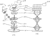
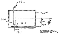
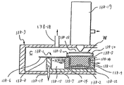
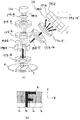
以上のような背景から作られたのが、図19に示すようなチャッキング機構である。静電チャックには、ウェーハWを安定に吸着するために櫛歯状に入り組んだ形状であることが望ましい電極19・1、19・2と、ウェーハ受渡し用の3本のプッシャーピン19・3と、ウェーハ印可用の2つ以上の導通針19・4とが設けられている。また、静電チャックの周囲には補正リング19・5とウェーハ落とし込み機構19・6が配置される。 The chucking mechanism as shown in FIG. 19 is made from the above background. The electrostatic chuck preferably has electrodes 19 1 and 19 2 which are desirably comb-shaped to stably attract the wafer W, and three pusher pins 19.3 for wafer transfer. , Two or more conducting needles 19.4 for wafer application. A correction ring 19.5 and a wafer drop mechanism 19.6 are arranged around the electrostatic chuck.
プッシャーピン19・3は、ウェーハWがロボットハンドによって搬送される際に静電チャック面上から予め突出しており、ロボットハンドの動作によってウェーハWがその上に載置されると、ゆっくりと下降し、ウェーハWを静電チャック上に載せる。ウェーハを静電チャック上から取出す際には逆の動作をしてロボットハンドにウェーハWを渡す役割を果たす。プッシャーピン19・3は、ウェーハ位置がずれたり汚染されることが無いよう表面材料を選ばなければならず、シリコンゴム、フッ素ゴム、SiCやアルミナ等のセラミックス、テフロン(登録商標)やポリイミド等の樹脂などを使用することが望ましい。 The pusher pins 19.3 protrude in advance from the electrostatic chuck surface when the wafer W is carried by the robot hand, and slowly move down when the wafer W is placed thereon by the operation of the robot hand. Then, the wafer W is placed on the electrostatic chuck. When the wafer is taken out from the electrostatic chuck, the wafer W is transferred to the robot hand by performing the reverse operation. For the pusher pins 19.3, a surface material must be selected so that the wafer position is not shifted or contaminated. Silicone rubber, fluorine rubber, ceramics such as SiC and alumina, Teflon (registered trademark), polyimide, and the like are used. It is desirable to use a resin or the like.
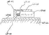
プッシャーピン19・3の駆動機構としては幾つか方法がある。一つは、静電チャックの下部に非磁性アクチュエータを設置する方法である。これは、超音波リニアモータによりプッシャピンを直接リニア駆動する方法や、回転形超音波モータとボールネジまたはラック&ピニオンギアの組合わせでプッシャピンの直線駆動を行う等の方法が有り得る。この方法は、静電チャックを搭載するXYステージのテーブル上に、プッシャ機構がコンパクトにまとめらる反面、アクチュエータやリミットセンサ等の配線が非常に多くなってしまう。これらの配線はXY動作するテーブルから試料室(メインチャンバ又は主ハウジング)壁面まで繋がるが、ステージの動作に伴って屈曲するため、大きな曲げRを持たせて配設する必要がありスペースをとってしまう。またパーティクル発生源になったり、配線の定期的な交換も必要になるので、使用数は必要最小限にするのがよい。 There are several methods for driving the pusher pins 19.3. One is a method of installing a non-magnetic actuator below the electrostatic chuck. This can be a method of directly linearly driving the pusher pin by an ultrasonic linear motor, or a method of linearly driving the pusher pin by a combination of a rotary ultrasonic motor and a ball screw or a rack and pinion gear. In this method, the pusher mechanism is compactly arranged on the table of the XY stage on which the electrostatic chuck is mounted, but the wiring of the actuator, the limit sensor, and the like becomes extremely large. These wirings are connected from the XY operating table to the wall surface of the sample chamber (main chamber or main housing), but they are bent with the operation of the stage, so they need to be arranged with a large bend R and take up space. I will. In addition, it becomes a source of particles, and it is necessary to periodically replace the wiring.
そこで別方式として、外部から駆動力を供給する方法もある。ウェーハWを着脱する位置にステージが移動すると、ベローズを介して真空中に突出した軸が、チャンバ外に備えられたエアシリンダで駆動されて、静電チャック下部に設けられたプッシャ駆動機構の軸を押すようになっている。軸はプッシャ駆動機構内部で、ラック・ピニオンまたはリンク機構と繋がっており、軸の往復移動がプッシャピンの上下動と連動するようになっている。ウェーハWをロボットハンドとの間で受け渡しする際には、コントローラで適切な速度に調整してエアシリンダで軸を真空中に押し出すことによって、プッシャーピン19・3を上昇させる。 Therefore, as another method, there is a method of supplying a driving force from the outside. When the stage is moved to a position where the wafer W is attached / detached, a shaft protruding into a vacuum through the bellows is driven by an air cylinder provided outside the chamber, and a shaft of a pusher driving mechanism provided below the electrostatic chuck. Is pressed. The shaft is connected to a rack and pinion or a link mechanism inside the pusher driving mechanism, so that reciprocating movement of the shaft is linked to vertical movement of the pusher pin. When transferring the wafer W to and from the robot hand, the pusher pins 19.3 are raised by adjusting the controller to an appropriate speed and pushing the shaft into a vacuum with an air cylinder.
なお、外部からの軸の駆動源は、エアシリンダに限るものではなく、サーボモータとラック・ピニオンやボールネジの組合わせでも良い。また、外部からの駆動源を回転軸とすることも可能である。その場合、回転軸は磁性流体シール等の真空シール機構を介し、プッシャ駆動機構は回転をプッシャの直線運動に変換する機構を内蔵する。 The drive source of the shaft from outside is not limited to the air cylinder, but may be a combination of a servo motor and a rack and pinion or a ball screw. It is also possible to use an external drive source as the rotation axis. In that case, the rotary shaft is provided via a vacuum seal mechanism such as a magnetic fluid seal, and the pusher drive mechanism has a built-in mechanism for converting rotation into linear motion of the pusher.
補正リング19・5は、ウェーハ端部の電界分布を均一に保つ作用を持つもので、基本的にウェーハと同電位を印可する。しかし、ウェーハと補正リング間の微小すきまや、ウェーハと補正リング表面高さの微小な差の影響を打ち消すため、ウェーハ端部電位と若干異なる電位を印可することもある。補正リングは、ウェーハの半径方向10〜30mm程度の幅を持ち、非磁性で導電性の材料、例えば、チタン、りん青銅、TiN又はTiCコーティングしたアルミ等を使用することができる。 The correction ring 19.5 has the function of keeping the electric field distribution at the edge of the wafer uniform, and basically applies the same potential as the wafer. However, a potential slightly different from the potential at the end of the wafer may be applied in order to cancel the influence of the minute gap between the wafer and the correction ring and the minute difference between the surface heights of the wafer and the correction ring. The correction ring has a width of about 10 to 30 mm in the radial direction of the wafer, and can be made of a non-magnetic and conductive material such as aluminum coated with titanium, phosphor bronze, TiN or TiC.
導通針19・4はばね19・7で支持されており、ウェーハが静電チャック上に搭載されると、ばね力でウェーハ裏面に軽く押し付けられる。この状態で、上述した様に電圧を印可することによってウェーハWとの電気的導通をとる。
The conducting needles 19 and 4 are supported by
静電チャック本体は、タングステン等の非磁性の平面状電極19・1、19・2と、その上に形成された誘電体から成る。誘電体の材料はアルミナ、窒化アルミ、ポリイミド等が使用できる。一般にアルミナ等のセラミックスは体積抵抗率が1014Ωcm程度の完全な絶縁体なので、材料内部での電荷移動は発生せず、吸着力としてクーロン力が作用する。これに対して、セラミックス組成をわずかに調整することによって体積抵抗率を1010Ωcm程度にすることができ、こうすることによって材料内部で電荷の移動が生じるため、ウェーハ吸着力としてクーロン力より強い所謂ジョンソン・ラーベック力が作用する。吸着力が強ければその分、印可電圧を低くすることができ、絶縁破壊に対するマージンを大きくとることができ、かつ安定した吸着力も得やすい。また、静電チャック表面をたとえばディンプル状に加工することによって、静電チャック表面にパーティクル等が付着しても、パーティクルがディンプルの谷部分に落ちる可能性が生じるのでウェーハの平面度に影響を与える可能性が減少する効果も期待できる。 The electrostatic chuck body is composed of non-magnetic planar electrodes 19 1 and 19 2 such as tungsten and a dielectric formed thereon. Alumina, aluminum nitride, polyimide or the like can be used as the material of the dielectric. Generally, ceramics such as alumina are perfect insulators having a volume resistivity of about 10 14 Ωcm, so that charge transfer does not occur inside the material, and Coulomb force acts as an attraction force. On the other hand, by slightly adjusting the ceramic composition, the volume resistivity can be reduced to about 10 10 Ωcm, and charge transfer occurs inside the material by doing so, so that the wafer adsorption force is stronger than the Coulomb force. The so-called Johnson-Rahbek force acts. If the attraction force is strong, the applied voltage can be reduced accordingly, a margin for insulation breakdown can be increased, and a stable attraction force can be easily obtained. Further, by processing the surface of the electrostatic chuck into, for example, a dimple shape, even if particles and the like adhere to the surface of the electrostatic chuck, the particles may fall to the valleys of the dimples, which affects the flatness of the wafer. The effect of reducing the possibility can also be expected.
以上より、静電チャック材料を、体積抵抗率を1010Ωcm程度に調整した窒化アルミやアルミナセラミックスとし、表面にディンプル状などの凹凸を形成し、その凸面の集合で形成される面の平面度を5μm程度に加工したものが実用的である。 As described above, the electrostatic chuck material is aluminum nitride or alumina ceramics whose volume resistivity is adjusted to about 10 10 Ωcm, and irregularities such as dimples are formed on the surface. Is practically processed to about 5 μm.
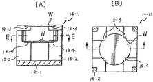
2−1−7−2)200/300ブリッジツールのためのチャッキング機構
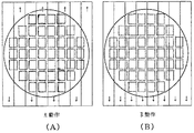
200mmと300mmの2種類のウェーハを機械的改造無く検査することが装置に求められることがある。その場合、静電チャックは2種類のサイズのウェーハをチャッキングし、かつウェーハ周縁部にウェーハのサイズに合わせた補正リングを載置しなければならない。図19の(A)、(B)及び図20はそのための構造を示している。
2-1-7-2) Chucking mechanism for 200/300 bridge tool The apparatus may be required to inspect two types of wafers, 200 mm and 300 mm, without mechanical modification. In that case, the electrostatic chuck must chuck wafers of two different sizes, and mount a correction ring according to the size of the wafer on the periphery of the wafer. FIGS. 19A, 19B and 20 show a structure for that purpose.
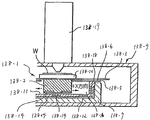
図19の(A)は静電チャック上に300mmのウェーハWを搭載した状態を示している。ウェーハWのサイズより僅かに大きい(隙間0.5mm程度)内径を持った補正リング19・1が、静電チャック外周の金属性リング状部品にインローで位置決めされ載置されている。この補正リング19・1には、ウェーハ落し込み機構19・2が3ヵ所設けられている。ウェーハ落し込み機構19・2は、プッシャーピン19・3の駆動機構と連動した上下駆動機構によって駆動され、補正リング19・1に設けられた回転軸周りに回転可能に支持されている。 FIG. 19A shows a state where a 300 mm wafer W is mounted on the electrostatic chuck. A correction ring 19.1 having an inner diameter slightly larger than the size of the wafer W (a gap of about 0.5 mm) is positioned and mounted on a metal ring-shaped part on the outer periphery of the electrostatic chuck by a spigot. The correction ring 19.1 is provided with three wafer dropping mechanisms 19.2. The wafer drop mechanism 19.2 is driven by a vertical drive mechanism interlocked with the drive mechanism of the pusher pin 19.3, and is rotatably supported around a rotation axis provided on the correction ring 19.1.
ウェーハWをロボットハンドから受ける場合、プッシャーピン駆動機構が動作し、プッシャーピン19・3を上に押上げる。それと適切なタイミングをとって補正リング19・1に設けられたウェーハ落し込み機構19・2も、図19の(B)に示すように、駆動力を受けて回転する。するとウェーハ落し込み機構19・2がウェーハWを静電チャック中心にガイドするテーパ面を形成する。次に、押し上げられたプッシャーピン19・3にウェーハWが載せられた後、プッシャーピン19・3を下降させる。ウェーハ落し込み機構19・2に対する駆動力の作用タイミングをプッシャーピン19・3の下降と適切に調整することによって、ウェーハWは落し込み機構19・2のテーパ面によって位置を修正されながら静電チャック上にウェーハWの中心と静電チャックの中心がほぼ一致するように置かれる。 When receiving the wafer W from the robot hand, the pusher pin driving mechanism operates to push up the pusher pins 19.3. At an appropriate timing, the wafer drop-in mechanism 19-2 provided on the correction ring 19-1 also receives the driving force and rotates as shown in FIG. Then, the wafer drop mechanism 19.2 forms a tapered surface that guides the wafer W to the center of the electrostatic chuck. Next, after the wafer W is placed on the pushed pusher pins 19.3, the pusher pins 19.3 are lowered. By appropriately adjusting the operation timing of the driving force to the wafer dropping mechanism 19.2 with the lowering of the pusher pin 19.3, the wafer W is corrected in position by the tapered surface of the wafer dropping mechanism 19.2 while the electrostatic chuck is adjusted. It is placed on the wafer W such that the center of the wafer W and the center of the electrostatic chuck substantially coincide with each other.
落し込み機構19・2のテーパ面にはテフロン(登録商標)等の低摩擦材、好ましくは導電性のある低摩擦材(例えば、導電性テフロン(登録商標)、導電性ダイヤモンドライクカーボン、TINコーティング)を形成することが望ましい。なお、図の符号A、B、C、D、Eは電圧を印加するための(後述する)端子であり、19・4はウェーハWが静電チャック上に載置されたことを検知するウェーハ導通用針で、バネ19・5によって押し上げられている。 A low friction material such as Teflon (registered trademark), preferably a low friction material having conductivity (for example, conductive Teflon (registered trademark), conductive diamond-like carbon, TIN coating) is provided on the tapered surface of the drop mechanism 19.2. ) Is desirably formed. Reference numerals A, B, C, D, and E in the figure denote terminals for applying a voltage (to be described later), and 19.4 denotes a wafer for detecting that the wafer W is mounted on the electrostatic chuck. The conducting needle is pushed up by the spring 19.5.
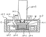
図20は、同じ静電チャックに200mmのウェーハWを搭載した状態を示している。静電チャックよりもウェーハ径が小さいため、静電チャック表面が露出してしまうので、静電チャックを完全に隠す大きさを持った補正リング20・1を搭載している。補正リング20・1の位置決めは300mm用補正リングの場合と同様である。
FIG. 20 shows a state where a 200 mm wafer W is mounted on the same electrostatic chuck. Since the wafer diameter is smaller than that of the electrostatic chuck, the surface of the electrostatic chuck is exposed. Therefore, the
補正リング20・1の内周部には段差が設けてあり、静電チャック側のリング状溝20・2に収まるようになっている。これは、200mmウェーハを搭載した時に補正リング20・1の内周とウェーハWの外周との間の隙間から静電チャック表面が見えないように導体(補正リング20・1)で隠すための構造である。もし静電チャック表面が見える構造になっていると、電子ビームが照射された際、静電チャック表面に電荷がチャージしてしまい、試料面の電位が乱れてしまうからである。
A step is provided on the inner peripheral portion of the
補正リング20・1の交換は、真空チャンバ内の所定の位置に補正リング交換場所を設けておき、そこから必要な大きさの補正リングをロボットによって搬送して静電チャックに取りつける(インロー部に挿入する)ことによって行う。 When replacing the correction ring 20.1, a correction ring replacement place is provided at a predetermined position in the vacuum chamber, and a correction ring of a required size is transported by the robot from there, and is attached to the electrostatic chuck (to the spigot portion). Insertion).
200mm用補正リングにも、300mmと同様にウェーハ落し込み機構20・2が設けられている。静電チャック側には、このウェーハ落し込み機構20・2と干渉しないように逃げが形成されている。静電チャック上へのウェーハの搭載方法は300mmの場合とまったく同様である。なお、符号A、B、C、D、Eは電圧を印加するための端子、20・3はプッシュピン19・3と同様のプッシュピン、20・4はウェーハ導通用針19・4と同様のウェーハ導通用針である。
The 200 mm correction ring is also provided with a wafer drop-in
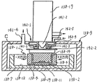
図20−1の(A)及び(B)は、300mmウェーハと200mmウェーハの両方に対応することができる静電チャックの構成を概略的に示した図であり、(A)は300mmウェーハを、(B)は200mmウェーハを載置した状態をそれぞれ示している。図20−1の(A)から理解されるとおり、静電チャックは300mmウェーハを載置することができる広さを持ち、図21−2の(B)に示すように、静電チャックの中央の部分は200mmウェーハを載置することができる広さであり、それを囲むように、補正リング20・1の内周部が嵌り込む溝20・6が設けられる。なお、符号A、B、C、D、Eは電圧を印加するための端子である。
FIGS. 20A and 20B are diagrams schematically illustrating a configuration of an electrostatic chuck capable of coping with both a 300 mm wafer and a 200 mm wafer. FIG. (B) shows a state in which a 200 mm wafer is placed. As can be understood from FIG. 20A, the electrostatic chuck has a space capable of mounting a 300 mm wafer, and as shown in FIG. Is large enough to mount a 200 mm wafer, and is provided with
図20−1の(A)及び(B)に示す静電チャックの場合、ウェーハが静電チャックに載置されているかどうか、ウェーハが静電チャックに正しく載置されたかどうか、補正リングがあるかどうか等は、光学的に検出される。例えば、静電チャックの上方に光学センサを設置し、その光学センサから発された光がウェーハによって反射されて再び光学センサへ戻ったときの光路長を検出することによって、ウェーハが水平に載置されたか、傾いて載置されたかが検出できる。また、補正リングの有無は、補正リングが載置されるべき場所の中の適宜の点を斜めに照射する光送信機と、補正リングからの反射光を受光する光受信機とを設けることで検出することができる。更に、200mmウェーハ用の補正リングが載置される場所の適宜の点を斜めに照射する光送信機及び該補正リングからの反射光を受光する光受信機の組み合わせと、300mmウェーハ用の補正リングが載置される場所の適宜の点を斜めに照射する光送信機及び該補正リングからの反射光を受光する光受信機の組み合わせとを設け、いずれの光受信機が反射光を受信するかを検知することにより、200mmウェーハ用の補正リングと300mmウェーハ用の補正リングのいずれが静電チャックに載置されたかを検出することができる。 In the case of the electrostatic chuck shown in FIGS. 20A and 20B, there is a correction ring whether the wafer is mounted on the electrostatic chuck, whether the wafer is correctly mounted on the electrostatic chuck, or not. Whether or not is detected optically. For example, by placing an optical sensor above the electrostatic chuck and detecting the optical path length when the light emitted from the optical sensor is reflected by the wafer and returned to the optical sensor again, the wafer is placed horizontally. It can be detected whether the camera has been placed or tilted. In addition, the presence or absence of the correction ring can be determined by providing an optical transmitter that irradiates an oblique point at an appropriate point in a place where the correction ring is to be mounted, and an optical receiver that receives light reflected from the correction ring. Can be detected. Further, a combination of an optical transmitter for obliquely irradiating an appropriate point of a place where a correction ring for a 200 mm wafer is mounted and an optical receiver for receiving reflected light from the correction ring, and a correction ring for a 300 mm wafer And a combination of an optical transmitter that irradiates an appropriate point of the place where the light is placed obliquely and an optical receiver that receives the reflected light from the correction ring, and which optical receiver receives the reflected light. Is detected, it is possible to detect which of the correction ring for the 200 mm wafer and the correction ring for the 300 mm wafer is placed on the electrostatic chuck.
2−1−7−3)ウェーハチャッキング手順
以上説明した構造をもったウェーハチャッキング機構は、以下の手順でウェーハをチャッキングする。
(1)ウェーハサイズに合った補正リングをロボットによって搬送し、静電チャックに搭載する。
(2)ロボットハンドによるウェーハ搬送とプッシャーピンの上下動によって、ウェーハを静電チャック上に載置する。
(3)静電チャックを双極形で印加(端子C、Dに正負逆の電圧を印加)し、ウェーハを吸着する。
(4)導通用針に所定電圧を印加し、ウェーハ裏面の絶縁膜(酸化膜)を破壊する。
(5)端子A、B間の電流を測定し、ウェーハとの導通が取れたかどうか確認する。
(6)静電チャックを単極形吸着に移行する。(端子A、BをGRD、端子C、Dに同一電圧を印加する)
(7)端子A(、B)と端子C(、D)との電位差を保ったまま端子A(、B)の電圧を下げ、ウェーハに所定のリターディング電圧を印加する。
2-1-7-3) Wafer chucking procedure The wafer chucking mechanism having the structure described above chucks a wafer in the following procedure.
(1) A correction ring suitable for a wafer size is transported by a robot and mounted on an electrostatic chuck.
(2) The wafer is placed on the electrostatic chuck by wafer transfer by the robot hand and vertical movement of the pusher pin.
(3) The electrostatic chuck is applied in a bipolar form (applied positive and negative voltages to terminals C and D) to attract the wafer.
(4) A predetermined voltage is applied to the conduction needle to break the insulating film (oxide film) on the back surface of the wafer.
(5) The current between the terminals A and B is measured, and it is confirmed whether or not conduction with the wafer has been established.
(6) Transfer the electrostatic chuck to the single-pole type suction. (GRD is applied to terminals A and B, and the same voltage is applied to terminals C and D)
(7) While maintaining the potential difference between the terminals A (, B) and the terminals C (, D), the voltage at the terminals A (, B) is reduced, and a predetermined retarding voltage is applied to the wafer.
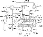
2−1−8)200/300ブリッジツールのための装置構成
200mmウェーハと300mmウェーハのどちらも機械的改造なしに検査できる装置にするための構成を図21及び図22に示す。以下、200mmウェーハもしくは300mmウェーハの専用装置と異なる点を説明する。
2-1-8) Apparatus configuration for 200/300 bridge tool FIGS. 21 and 22 show a configuration for making an apparatus capable of inspecting both a 200 mm wafer and a 300 mm wafer without mechanical modification. Hereinafter, differences from the dedicated apparatus for a 200 mm wafer or a 300 mm wafer will be described.
200/300mmウェーハ、FOUP、SMIF、オープンカセット等の仕様毎に交換されるウェーハカセットの設置場所21・1には、ユーザー仕様によって決まるウェーハサイズやウェーハカセットの種類に応じたウェーハカセットが設置できるようになっている。大気搬送ロボット21・2は、異なるウェーハサイズに対応できるようなハンドを備え、すわなちウェーハの落し込み部がウェーハサイズに合わせて複数設けられており、ウェーハサイズにあった箇所でハンドに搭載されるようになっている。大気搬送ロボット21・2はウェーハを設置場所21・1からプリアライナ21・3へ送ってウェーハの向きを整えた後、ウェーハをプリアライナ21・3から取り出して、ロードロック室21・4内へ送る。
The wafer cassette installation location 21.1 which is exchanged for each specification such as 200/300 mm wafer, FOUP, SMIF, open cassette, etc., can be set in accordance with the wafer size determined by the user specification and the type of wafer cassette. It has become.
ロードロック室21・4の内部のウェーハラックも同様の構造で、ウェーハラックのウェーハ支持部には、ウェーハサイズに合わせた複数の落し込み部が形成されており、大気搬送ロボット21・2のハンドに搭載されたウェーハは、そのサイズに合った落し込み部に搭載されるようにロボットハンドの高さが調整されてウェーハラック内にウェーハが挿入され、その後、ロボットハンドが下降することによってウェーハ支持部の所定の落し込み部にウェーハが載置される。 The wafer rack inside the load lock chambers 21.4 has the same structure, and a plurality of recesses corresponding to the wafer size are formed in the wafer support portion of the wafer rack. The height of the robot hand is adjusted so that the wafer mounted on the wafer is mounted in the dropping part corresponding to its size, the wafer is inserted into the wafer rack, and then the wafer hand is lowered by lowering the robot hand. The wafer is placed in a predetermined recess of the section.
ロードロック室21・4内のウェーハラックに載置されたウェーハは、次いで、搬送室21・5内に設置された真空搬送ロボット21・6によってロードロック室21・3から取り出されて試料室21・7内のステージ21・8上に搬送される。真空搬送ロボット21・6のハンドも、大気搬送ロボット21・2と同様、ウェーハサイズに合った複数の落し込み部を有している。ロボットハンドの所定の落し込み部に搭載されたウェーハは、ステージ21・8において、予めウェーハサイズに合った補正リング21・9を搭載した静電チャック上に載置され、静電チャックで吸着固定される。補正リング21・9は、搬送室21・5内に設けられた補正リングラック21・10上に載置されている。そこで、真空搬送ロボット21・6はウェーハサイズに合った補正リング21・9を補正リングラック21・10から取り出して静電チャック上に搬送し、静電チャック外周部に形成された位置決め用インロー部に補正リング21・9を嵌め込んでから、ウェーハを静電チャックに載置する。
The wafers placed on the wafer racks in the load lock chambers 21.4 are then taken out of the load lock chambers 21.3 by the vacuum transfer robots 21.6 installed in the transfer chambers 21.5, and the sample chambers 21 are removed. -It is conveyed on the stage 21.8 in 7. The hands of the
補正リングを交換する時は、この逆の操作を行う。すなわち、ロボット21・6によって静電チャックから補正リング21・9を外し、搬送室21・5内の補正リングラック21・10に補正リングを戻し、これから検査するウェーハサイズにあった補正リングを補正リングラック21・10から静電チャックまで搬送する。 When replacing the correction ring, perform the reverse operation. That is, the correction ring 21.9 is removed from the electrostatic chuck by the robot 21.6, and the correction ring is returned to the correction ring rack 21.10 in the transfer chamber 21.5, and the correction ring corresponding to the wafer size to be inspected is corrected. It is transported from the ring racks 21 and 10 to the electrostatic chuck.
図21に示す検査装置のおいては、プリアライナ21・3がロードロック室22・4の近くに配置されているので、ウェーハのアライメントが不十分なためにロードロック室で補正リングが装着できない場合にも、ウェーハをプリアライナに戻してアライメントし直すことが容易であり、工程での時間のロスを減らせるという利点がある。
In the inspection apparatus shown in FIG. 21, since the pre-aligners 21 and 3 are disposed near the
図22は、補正リングの置き場所を変えた例であり、補正リングラック21・10は省略されている。ロードロック室22・1には、ウェーハラックと補正リングラックとが階層的に形成されており、これらはエレベータに設置されて上下動することができる。まず、これから検査するウェーハサイズに合った補正リングを静電チャックに設置するため、真空搬送ロボット21・6が該補正リングを取出せる位置までロードロック室22・1のエレベータを移動する。そして補正リングを真空搬送ロボット21・6で静電チャック上に設置すると、今度は、検査すべきウェーハを搬送できるようにエレベータを操作し、ウェーハを真空搬送ロボット21・6でウェーハラックから取出した後、静電チャックに載置する。この構成の場合、ロードロック室22・1にエレベータが必要になるが、真空の搬送室21・5を小さく形成することができ、装置のフットプリントを小さくする上で有効である。 FIG. 22 shows an example in which the position of the correction ring is changed, and the correction ring racks 21 and 10 are omitted. In the load lock chamber 22.1, a wafer rack and a correction ring rack are formed in a hierarchy, and these are installed in an elevator and can move up and down. First, the elevator of the load lock chamber 22.1 is moved to a position where the vacuum transfer robots 21.6 can take out the correction ring in order to install a correction ring corresponding to the wafer size to be inspected on the electrostatic chuck. When the correction ring was set on the electrostatic chuck by the vacuum transfer robots 21.6, the elevator was operated so that the wafer to be inspected could be transferred, and the wafer was removed from the wafer rack by the vacuum transfer robots 21.6. Then, it is mounted on the electrostatic chuck. In this configuration, an elevator is required for the load lock chamber 22.1. However, the vacuum transfer chamber 21.5 can be formed small, which is effective in reducing the footprint of the apparatus.
なお、静電チャック上にウェーハが存在するか否かを検知するセンサは、異なるウェーハサイズのどちらにも対応できる位置に設置されることが望ましいが、それが不可能な場合には、同一の働きをする複数のセンサをウェーハサイズ毎に配置してもよい。 The sensor for detecting whether or not a wafer exists on the electrostatic chuck is desirably installed at a position that can support both different wafer sizes, but when it is not possible, the same sensor is used. A plurality of working sensors may be arranged for each wafer size.
図21に関して述べた検査装置においては、静電チャックの上に補正リングを載置し、その補正リングの内径に当てはまるようにウェーハを位置決めするという手順が取られている。そこで、図22に示す検査装置においては、ロードロック室22・1でウェーハに補正リングを装着し、補正リングが装着されたウェーハを補正リングごと搬送して試料室21・7へ導入し、ステージ上の静電チャックに装着するという手順が取られる。それを実現する機構として、図22−1及び図22−2に示す、エレベータを上下させてウェーハを大気搬送ロボットから真空搬送ロボットへ渡すためのエレベータ機構がある。以下、この機構を用いてウェーハを搬送する手順を説明する。 In the inspection apparatus described with reference to FIG. 21, a procedure is adopted in which a correction ring is placed on an electrostatic chuck and the wafer is positioned so as to fit the inner diameter of the correction ring. Therefore, in the inspection apparatus shown in FIG. 22, a correction ring is mounted on the wafer in the load lock chamber 22.1, and the wafer on which the correction ring is mounted is transported together with the correction ring and introduced into the sample chamber 21.7. The procedure of mounting on the upper electrostatic chuck is taken. As a mechanism for realizing this, there is an elevator mechanism shown in FIGS. 22-1 and 22-2 for raising and lowering an elevator to transfer a wafer from an atmospheric transfer robot to a vacuum transfer robot. Hereinafter, a procedure of transferring a wafer using this mechanism will be described.
図22−1の(A)に示すように、ロードロック室の中に設けられたエレベータ機構は上下方向に移動可能に設けられた複数段(図では2段)の補正リング支持台を有する。上段の補正リング支持台22・2と下段の補正リング支持台22・3とは、第1のモータ22・4の回転によって昇降する第1の台22・5に固定され、これによって、第1のモータ22・4の回転により、第1の台22・5及び上下の補正リング支持台22・2、22・3が上方又は下方に移動することになる。 As shown in FIG. 22A, the elevator mechanism provided in the load lock chamber has a plurality of (two in the figure) correction ring supports movably provided in the vertical direction. The upper correction ring support 22.2 and the lower correction ring support 22.3 are fixed to the first base 22.5 which moves up and down by the rotation of the first motor 22.4. The rotation of the motor 22.4 moves the first base 22.5 and the upper and lower correction ring support bases 22.2 and 22.3 upward or downward.
各補正リング支持台にはウェーハのサイズに応じた内径の補正リング22・6が載置されている。補正リング22・6は200mmウェーハ用と300mmウェーハ用との、内径が異なる2種類が用意され、これらの補正リングの外径は同じである。このように、同じ外径の補正リングを用いることにより、相互互換性が生まれ、ロードロック室の中に200mm用と300mm用とを自由な組み合わせで載置しておくことが可能になる。つまり、200mmウェーハと300mmウェーハとが混合して流れてくるラインについては、上段を300mm用、下段を200mm用とし、どちらのウェーハが流れてきても検査を行えるよう柔軟に対応することができる。また、同じサイズのウェーハが流れてくるラインであれば、上下の段を200mm用或いは300mm用とし、上下の段のウェーハを交互に検査することができるので、スループットを向上させることができる。 On each correction ring support, a correction ring 22.6 having an inner diameter corresponding to the size of the wafer is mounted. Two types of correction rings 2 and 6 having different inner diameters for a 200 mm wafer and a 300 mm wafer are prepared, and the outer diameters of these correction rings are the same. As described above, by using the correction rings having the same outer diameter, mutual compatibility is created, and it becomes possible to place the 200 mm and 300 mm free combinations in the load lock chamber. In other words, for a line in which a 200 mm wafer and a 300 mm wafer are mixed and flow, the upper stage is used for 300 mm and the lower stage is used for 200 mm, so that inspection can be performed flexibly so that inspection can be performed regardless of which wafer flows. In addition, if the same size wafer flows, the upper and lower stages can be used for 200 mm or 300 mm, and the upper and lower stages can be inspected alternately, so that the throughput can be improved.
第1の台22・5には第2のモータ22・7が載置され、第2のモータ22・7には第2の台22・8が昇降可能に取り付けられている。第2の台22・8には上段のウェーハ支持台22・9と下段のウェーハ支持台22・10とが固定されている。これにより、第2のモータ22・7が回転すると、第2の台22・8と上下のウェーハ支持台22・9、22・10とが一体に上方又は下方に移動することになる。
A second motor 22.7 is mounted on the first table 22.5, and a second table 22.8 is mounted on the second motor 22.7 so as to be able to move up and down. An
そこで、図22−1の(A)に示すように、ウェーハWを大気搬送ロボット21・2のハンドに載せてロードロック室22・1に搬入し、次いで、(B)に示すように、第2のモータ22・7を第1の方向に回転させてウェーハ支持台22・9、22・10を上方に移動させ、ウェーハWを上段のウェーハ支持台22・9の上に載置させる。これによって、ウェーハWを大気搬送ロボット21・2からウェーハ支持台22・9へ移す。その後、(C)に示すように大気搬送ロボット21・2を後退させ、大気搬送ロボット21・2の後退が完了したところで、(D)に示すように、第2のモータ22・7を第1の方向とは逆の方向に回転させてウェーハ支持台22・9、22・10を下方へ移動させる。これによってウェーハWは上段の補正リング22・6に載置される。
Then, as shown in FIG. 22A, the wafer W is loaded on the hand of the atmospheric transfer robot 21.2 and loaded into the load lock chamber 22.1. Then, as shown in FIG. The second motor 22.7 is rotated in the first direction to move the wafer supports 20.9, 22.10 upward, and the wafer W is placed on the upper wafer support 22.9. As a result, the wafer W is transferred from the atmospheric transfer robot 21.2 to the wafer support 22.9. Thereafter, as shown in (C), the atmospheric transfer robot 21.2 is retracted. When the retreat of the atmospheric transfer robot 21.2 is completed, as shown in (D), the
次いで、(E)に示すように、真空搬送ロボット21・6のハンドをロードロック室22・1の中に入れて補正リング22・6の下側で停止させる。この状態で第1のモータ22・4を回転させ、(F)に示すように、第1の台22・5、上下の補正リング支持台22・2、22・3、第2のモータ22・7及び上下のウェーハ支持台22・9、22・10を下方へ移動させ、これによって、上段のウェーハ支持台22・9に載置されていた補正リング21・6及びウェーハWを真空搬送ロボット21・6のハンドに載せ、試料室21・7へ搬入することができる。
Next, as shown in (E), the hands of the vacuum transfer robots 21.6 are put into the load lock chambers 22.1 and stopped below the correction rings 22.6. In this state, the first motor 22.4 is rotated, and as shown in (F), the first base 22.5, the upper and lower correction ring support bases 22.2 and 22.3, and the
試料室21・7での検査が終了したウェーハをロードロック室21・4へ戻す動作は、上記とは逆の手順で行われ、補正リングと共に真空搬送ロボットによりウェーハ支持台の上に搬入されたウェーハは、補正リング支持台に、次いでウェーハ支持台に移され、最後に大気搬送ロボットに載置されることになる。なお、図22−1及び図22−2においては、上段におけるウェーハ受け渡し動作を説明したが、大気搬送ロボット21・2及び真空搬送ロボット21・6のハンドの高さを調整することにより、下段においても同様の動作が可能である。このように大気搬送ロボット21・2及び真空搬送ロボット21・6のハンドの高さを適切に切り換えることにより、一方の段から未検査のウェーハを試料室へ搬入し、次いで検査済みのウェーハを試料室から他方の段へ搬出することを交互に行うことができる。
The operation of returning the wafer, which has been inspected in the
2−2)ウェーハの搬送方法
次に、カセットホルダ13・2に支持されたカセット13・12からワーキングチャンバ13・16内に配置されたステージ装置13・6までへのウェーハの搬送を順を追って説明する(図14〜図16参照)。
2-2) Wafer Transfer Method Next, wafer transfer from the
カセットホルダ13・2は、前述のように人手によりカセットをセットする場合にはそれに適した構造のものが、また自動的にカセットをセットする場合にはそれに適した構造のものが使用される。この実施の形態において、カセット13・12がカセットホルダ13・2の昇降テーブル13・13の上にセットされると、昇降テーブル13・13は昇降機構13・14によって降下されカセット13・12が出入り口13・15に整合される。カセットが出入り口13・15に整合されると、カセットに設けられたカバー(図示せず)が開き、カセットとミニエンバイロメント装置13・3の出入り口13・15との間には筒状の覆いが配置されてカセット内及びミニエンバイロメント空間内を外部から遮断する。これらの構造は公知のものであるから、その構造及び動作の詳細な説明は省略する。なお、ミニエンバイロメント装置13・3側に出入り口13・15を開閉するシャッタ装置が設けられている場合にはそのシャッタ装置が動作して出入り口13・15を開く。
As described above, the cassette holder 13.2 has a structure suitable for manually setting the cassette, and a structure suitable for automatically setting the cassette. In this embodiment, when the
一方、第1の搬送ユニット16・14のアーム16・16は方向M1又はM2のいずれかに向いた状態(この説明ではM1の方向)で停止しており、出入り口13・15が開くとアームが伸びて先端でカセット内に収容されているウェーハのうち1枚を受け取る。なお、アームと、カセットから取り出されるべきウェーハとの上下方向の位置調整は、この実施の形態では第1の搬送ユニット16・14の駆動部16・15及びアーム16・16の上下移動で行うが、カセットホルダの昇降テーブルの上下動行っても或いはその両者で行ってもよい。
On the other hand, the
アーム16・16によるウェーハの受け取りが完了すると、アームは縮み、シャッタ装置を動作して出入り口を閉じ(シャッタ装置がある場合)、次にアーム16・16は軸線O1−O1の回りで回動して方向M3に向けて伸長できる状態になる。すると、アームは伸びて先端に載せられ或いはチャックで把持されたウェーハをプリアライナー16・5の上に載せ、そのプリアライナー16・5によってウェーハの回転方向の向き(ウェーハ平面に垂直な中心軸線の回りの向き)を所定の範囲内に位置決めする。位置決めが完了すると搬送ユニット16・14はアームの先端にプリアライナー16・5からウェーハを受け取ったのちアームを縮ませ、方向M4に向けてアームを伸長できる姿勢になる。するとシャッタ装置14・8の扉13・27が動いて出入り口13・25及び13・37を開き、アーム16・16が伸びてウェーハを第1のローディングチャンバ14・2内のウェーハラック14・11の上段側又は下段側に載せる。なお、前記のようにシャッタ装置14・8を開いてウェーハラック14・11にウェーハが受け渡される前に、仕切壁14・5に形成された開口17・4はシャッタ装置14・10の扉14・19により気密状態で閉じられている。
When the
上記第1の搬送ユニット16・14によるウェーハの搬送過程において、ミニエンバイロメント装置13・3のハウジングの上に設けられた気体供給ユニット16・9からは清浄空気が層流状に流れ(ダウンフローとして)、搬送途中で塵埃がウェーハの上面に付着するのを防止する。搬送ユニット周辺の空気の一部(この実施の形態では供給ユニットから供給される空気の約20%で主に汚れた空気)は排出装置16・4の吸入ダクト16・12から吸引されてハウジング外に排出される。残りの空気はハウジングの底部に設けられた回収ダクト16・10を介して回収され再び気体供給ユニット16・9に戻される。
In the process of transferring wafers by the
ローダハウジング13・5の第1のローディングチャンバ14・2内のウェーハラック14・11内に第1の搬送ユニット16・14によりウェーハが載せられると、シャッタ装置14・8が閉じて、ローディングチャンバ14・2内を密閉する。すると、第1のローディングチャンバ14・2内には不活性ガスが充填されて空気が追い出された後、その不活性ガスも排出されてそのローディングチャンバ14・2内は真空雰囲気にされる。この第1のローディングチャンバ14・2の真空雰囲気は低真空度でよい。ローディングチャンバ14・2内の真空度がある程度得られると、シャッタ装置14・10が動作して扉14・19で密閉していた出入り口17・4のシャッタ14・5を開き、第2の搬送ユニット14・12のアーム14・20が伸びて先端の把持装置でウェーハ受け14・11から1枚のウェーハを受け取る(先端の上に載せて或いは先端に取り付けられたチャックで把持して)。ウェーハの受け取りが完了するとアームが縮み、シャッタ装置14・10が再び動作して扉14・19で出入り口17・4を閉じる。
When a wafer is placed by the
なお、シャッタ装置14・10が開く前にアーム14・20は予めウェーハラック14・11の方向N1に向けて伸長できる姿勢になる。また、前記のようにシャッタ装置14・10が開く前にシャッタ装置13・29の扉14・9で出入り口14・7、14・1を閉じていて、第2のローディングチャンバ14・3内とワーキングチャンバ13・16内との連通を気密状態で阻止しており、第2のローディングチャンバ14・3内は真空排気される。
Before the
シャッタ装置14・10が出入り口17・4を閉じると、第2のローディングチャンバ14・3内は再度真空排気され、第1のローディングチャンバ14・2内よりも高真空度の真空にされる。その間に、第2の搬送ユニット16・14のアームはワーキングチャンバ13・16内のステージ装置13・6の方向に向いて伸長できる位置に回転される。一方ワーキングチャンバ13・16内のステージ装置13・6では、Yテーブル13・33が、Xテーブル13・34の中心線X0−X0が第2の搬送ユニット14・12の回動軸線O2−O2を通るX軸線X1−X1とほぼ一致する位置まで、図14で上方に移動し、また、Xテーブル13・34は図14で最も左側の位置に接近する位置まで移動し、この状態で待機している。第2のローディングチャンバ14・3がワーキングチャンバ13・16の真空状態と略同じになると、シャッタ装置13・29の扉14・9が動いて出入り口14・7、14・1を開き、アームが伸びてウェーハを保持したアームの先端がワーキングチャンバ13・16内のステージ装置13・6に接近する。そしてステージ装置13・6の載置面14・14上にウェーハを載置する。ウェーハの載置が完了するとアームが縮み、シャッタ装置13・29が出入り口14・7、14・1を閉じる。
When the
ステージには、ウェーハに逆バイアス電位(リターディング電位)をかける機構があるので、アームがステージへウェーハを置きに行くもしくは取りに行く時、アームをステージと同じもしくは近い電位、またはアームをフローティング電位にしておくことにより、電位のショートによる放電などの不具合を避ける機構を有している。また、別の実施の形態として、ウェーハをステージ装置上に搬送する際にはウェーハへのバイアス電位をオフにしておいてもよい。 Since the stage has a mechanism to apply a reverse bias potential (retarding potential) to the wafer, when the arm goes to or picks up the wafer from the stage, the arm is at or near the stage potential, or the arm is at the floating potential. In this case, a mechanism is provided to avoid problems such as electric discharge due to short-circuit of the potential. In another embodiment, when a wafer is transferred onto a stage device, the bias potential to the wafer may be turned off.
バイアス電位を制御する場合には、ウェーハがステージに搬送されるまでは電位をオフにしておき、ステージに搬送され載置されてからオンにしてバイアス電位を印加するようにしてもよい。バイアス電位を印加する時機は、タクトタイムを予め設定しておき、それにしたがって印加してもよいし、ステージの上にウェーハが載置された事をセンサで検出し、その検出信号をトリガとして印加するようにしてもよい。また、シャッタ装置13・29が出入口14・7、14・1を閉じたことを検出して、その検出信号をトリガとして印加してもよい。更に、静電チャックを用いるばあには、静電チャックに吸着されたことを確認し、それをトリガとしてバイアス電位を印加するようにしてもよい。
When controlling the bias potential, the potential may be turned off until the wafer is transferred to the stage, and may be turned on after being transferred and mounted on the stage to apply the bias potential. When applying the bias potential, the tact time may be set in advance and applied in accordance therewith, or the sensor detects that the wafer is mounted on the stage and applies the detection signal as a trigger. You may make it. Alternatively, it may be detected that the
以上は、カセット13・12内のウェーハをステージ装置上に搬送するまでの動作について説明したが、ステージ装置13・6に載せられて処理が完了したウェーハをステージ装置13・6からカセット13・12内に戻すには前述と逆の動作を行って戻す。また、ウェーハラック14・11に複数のウェーハを載置しておくため、第2の搬送ユニット14・12でウェーハラック14・11とステージ装置13・6との間でウェーハの搬送を行う間に、第1の搬送ユニット16・14でカセットとウェーハラック14・11との間でウェーハの搬送を行うことができ、検査処理を効率良く行うことができる。
The operation up to the transfer of the wafers in the
具体的には、ウェーハラック14・11に、既に処理済のウェーハAと未処理のウェーハBがある場合、まず、ステージ装置13・6に未処理のウェーハBを移動する。この間に、処理済ウェーハAを、アームによりウェーハラックからカセット13・12に移動し、未処理のウェーハCを同じくアームによりカセット13・12から抜き出し、プリアライナ16・5で位置決めした後、ローディングチャンバ14・2のウェーハラック14・11に移動する。
Specifically, when there are already processed wafers A and unprocessed wafers B in the wafer racks 14 and 11, first, the unprocessed wafers B are moved to the stage devices 13.6. During this time, the processed wafer A is moved from the wafer rack to the
このようにすることで、ウェーハラック14・11の中は、ウェーハBを処理中に、処理済のウェーハAが未処理のウェーハCに置き換えることができる。また、検査や評価を行うこのような装置の利用の仕方によっては、ステージ装置13・6を複数台並列に置き、それぞれの装置に一つのウェーハラック14・11からウェーハを移動することで、複数枚のウェーハを同じ処理することもできる。
In this manner, in the wafer racks 14 and 11, the processed wafer A can be replaced with the unprocessed wafer C while the wafer B is being processed. In addition, depending on the use of such an apparatus for performing inspection and evaluation, a plurality of stage devices 13.6 are arranged in parallel, and wafers are moved from one
図23は、主ハウジング13・4の支持方法の変形例がで示されている。図23に示された変形例では、ハウジング支持装置23・1を厚肉で矩形の鋼板23・2で構成し、その鋼板の上にハウジング本体23・3が載せられている。したがって、ハウジング本体23・1の底壁23・4は、前記実施の形態の底壁に比較して薄い構造になっている。図24に示された変形例では、ハウジング支持装置24・1のフレーム構造体24・2によりハウジング本体24・3及びローダハウジング24・4を吊り下げて状態で支持するようになっている。
FIG. 23 shows a modified example of the method of supporting the
フレーム構造体24・2に固定された複数の縦フレーム24・5の下端は、ハウジング本体24・3の底壁24・6の四隅に固定され、その底壁により周壁及び頂壁を支持するようになっている。そして防振装置24・7は、フレーム構造体24・2と台フレーム24・8との間に配置されている。また、ローダハウジング24・4もフレーム構造体24・2に固定された吊り下げ部材24・9によって吊り下げられている。ハウジング本体24・3のこの図24に示された変形例では、吊り下げ式に支えるので主ハウジング及びその中に設けられた各種機器全体の低重心化が可能である。上記変形例を含めた主ハウジング及びローダハウジングの支持方法では主ハウジング及びローダハウジングに床からの振動が伝わらないようになっている。
The lower ends of the plurality of vertical frames 24.5 fixed to the frame structures 24.2 are fixed to the four corners of the bottom wall 24.6 of the housing body 24.3, and the bottom wall supports the peripheral wall and the top wall. It has become. The anti-vibration device 24.7 is disposed between the frame structure 24.2 and the base frame 24.8. The loader housings 24.4 are also suspended by suspension members 24.9 fixed to the frame structure 24.2. In the modified example of the
図示しない別の変形例では、主ハウジングのハウジング本体のみがハウジング支持装置によって下から支えられ、ローダハウジングは隣接するミニエンバイロメント装置13・3と同じ方法で床上に配置され得る。また、図示しない更に別の変形例では、主ハウジング13・4のハウジング本体のみがフレーム構造体に吊り下げ式で支持され、ローダハウジングは隣接するミニエンバイロメント装置と同じ方法で床上に配置され得る。
In another variant, not shown, only the housing body of the main housing is supported from below by the housing support device, and the loader housing can be arranged on the floor in the same way as the adjacent mini-environment devices 13.3. In yet another variant, not shown, only the housing bodies of the
上記の実施の形態によれば、次のような効果を奏することが可能である。
(1)電子線を用いた写像投影方式の検査装置の全体構成が得られ、高いスループットで検査対象を処理することができる。
(2)ミニエンバイロメント空間内で検査対象に清浄気体を流して塵埃の付着を防止すると共に清浄度を観察するセンサを設けることによりその空間内の塵埃を監視しながら検査対象の検査を行うことができる。
(3)ローディングチャンバ及びワーキングチャンバを一体的に振動防止装置を介して支持したので外部の環境に影響されずにステージ装置への検査対象の供給及び検査を行うことができる。
According to the above embodiment, the following effects can be obtained.
(1) The whole configuration of the inspection apparatus of the projection type using the electron beam can be obtained, and the inspection target can be processed with high throughput.
(2) Inspection of the inspection target while monitoring dust in the mini-environment space by monitoring the dust in the mini-environment space by providing a sensor for flowing a clean gas to the inspection target to prevent dust from adhering and observing the cleanliness. Can be.
(3) Since the loading chamber and the working chamber are integrally supported via the anti-vibration device, the inspection target can be supplied and inspected to the stage device without being affected by the external environment.
2−3)電子光学系
2−3−1)概要
電子光学系13・8は、ハウジング本体13・17に固定された鏡筒13・38の中に設けられた、図25−1に概略的に図示する一次電子光学系(以下、単に一次光学系という)25・1と、二次電子光学系(以下、単に二次光学系という)25・2とを備える電子光学系と、検出系25・3とを備える。一次光学系25・1は、電子線を検査対象であるウェーハWの表面に照射する光学系で、電子線を放出する電子銃25・4と、電子銃25・4から放出された一次電子線を集束する静電レンズからなるレンズ系25・5と、ウイーンフィルタすなわちE×B分離器25・6と、対物レンズ系25・7とを備え、それらは、図25−1に示されるように電子銃25・4を最上部にして順に配置されている。この実施の形態の対物レンズ系25・7を構成するレンズは減速電界型対物レンズである。この実施の形態では、電子銃25・4から放出される一次電子線の光軸は、検査対象であるウェーハWに照射される照射光軸(ウェーハの表面に垂直になっている)に関して斜めになっている。対物レンズ系25・7と検査対象であるウェーハWとの間には電極25・8が配置されている。この電極25・8は一次電子線の照射光軸に関して軸対称の形状になっていて、電源25・9によって電圧制御されるようになっている。
2-3) Electron optical system
2-3-1) Overview The electron optical system 13.8 is a primary electron optical system schematically illustrated in FIG. 25-1 provided in lens barrels 13 and 38 fixed to the
二次光学系25・2は、E×B型偏向器25・6により一次光学系から分離された二次電子を通す静電レンズから成るレンズ系25・10を備えている。このレンズ系25・10は二次電子像を拡大する拡大レンズとして機能する。
The secondary optical system 25.2 includes a
検出系25・3は、レンズ系25・10の結像面に配置された検出器25・11及び画像処理部25・12を備えている。
一次ビームの入射方向は通常E×BフィルタのE方向(電界の逆方向)であり、この方向と積算型のラインセンサ(TDI:time delay integration)の積算方向とは同じ方向となっている。TDIの積算方向は一次ビーム方向と異なっていても構わない。
The detection system 25.3 includes a detector 25.11 and an image processing unit 25.12 arranged on the image plane of the lens system 25.10.
The incident direction of the primary beam is usually the E direction of the E × B filter (the reverse direction of the electric field), and this direction is the same as the integration direction of the integration type line sensor (TDI: time delay integration). The integration direction of TDI may be different from the primary beam direction.
電子ビーム光学系鏡筒は以下の構成要素を備えている。
(1)コラム磁気シールド
鏡筒を構成する部材には望ましくはパーマロイ等のニッケル合金や鉄等の磁性体を用いると良く、磁気的な外乱の影響を抑える効果が期待できる。
The electron beam optical system lens barrel includes the following components.
(1) Column magnetic shield A magnetic material such as a nickel alloy such as permalloy or iron is desirably used as a member constituting the lens barrel, and an effect of suppressing the influence of magnetic disturbance can be expected.
(2)検出器回転機構
ステージの走査軸方向と検出器の走査方向とを一致させるために、鏡筒13・38の上部には、鏡筒13・38の内を真空に保持した状態のままTDI等の検出器25・11を光軸周りに±数度程度回転できるようにして、装置の組立により生じる走査方向のずれを無くす検出器回転機構を有している。この機構においては、回転分解能及び回転位置再現性は5〜40秒程度必要である。これは、検出器において、1フレーム分の画像を走査する間にステージの走査方向と検出器の走査方向とのずれを1ピクセルの1/10程度に収める必要から出てくる。検出器回転機構によれば、ステージの移動方向とTDIの積算方向の角度誤差を10mrad以下、好ましくは1mrad以下、より好ましくは0.2mrad以下に調整することも可能である。
(2) Detector rotation mechanism In order to make the scanning axis direction of the stage coincide with the scanning direction of the detector, the upper part of the lens barrels 13 and 38 is kept in a state where the inside of the lens barrels 13 and 38 is kept in vacuum. There is a detector rotation mechanism that enables the
以下、図25−3〜図25−5を用いて、検出器回転機構の構成の一例を説明する。図25−3は、鏡筒13・38の上部に設けられた検出器回転機構の全体の構成を示す図であり、図25−4は、上鏡筒を回転させるための機構の概略図であり、図25−5は、上鏡筒と下鏡筒とをシールするための機構を示している。 Hereinafter, an example of the configuration of the detector rotation mechanism will be described with reference to FIGS. 25-3 to 25-5. FIG. 25C is a diagram illustrating the entire configuration of the detector rotation mechanism provided above the lens barrels 13 and 38, and FIG. 25D is a schematic diagram of a mechanism for rotating the upper lens barrel. FIG. 25-5 shows a mechanism for sealing the upper lens barrel and the lower lens barrel.
図25−3において、鏡筒13・38の上端は、検出器25・11が取り付けられた上鏡筒25・20と、主ハウジング13・4に固定された下鏡筒25・21とからなる。上鏡筒25・20は下鏡筒25・21に対してベアリング25・22を介して支持されて二次光学系の光軸の周りに回転可能であり、また、上鏡筒25・20と下鏡筒25・21との間には、鏡筒13・38の内部を真空に保つためにシール部25・23が設けられる。具体的には、上鏡筒25・20の下端と下鏡筒25・21の上端との間にシール部25・23を設置するとともに、下鏡筒25・21の上端に上鏡筒25・20を取り囲むように鍔部25・24を設け、この鍔部25・24と上鏡筒25・20の側面との間にベアリング25・22を設置する。
In FIG. 25C, the upper ends of the lens barrels 13 and 38 include an
上鏡筒25・20と下鏡筒25・21とにはそれぞれ、ベアリング25・22を押さえるためのベアリング押さえ25・25、25・26がネジ止めされる。さらに、上鏡筒25・20を下鏡筒25・21に対して回転させるために、図25−4に示す駆動機構が設けられる。即ち、鍔部25・24の上端に設けられたベアリング押さえ25・26の一部には突起25・27が設けられ、一方、上鏡筒25・20から突設された取り付け部材(ブラケット)25・28にはアクチュエータ25・29が固定される。アクチュエータ25・29の軸25・30は突起25・27と接触し、鍔部25・24とアクチュエータ29・29が固定された取り付け部材(ブラケット)25・28との間には、突起25・27の方へ引く力が与えられた予圧バネ25・31が設けられる。これにより、アクチュエータ25・29を作動させて軸25・30がアクチュエータ25・29から突出する長さを変えることにより、下鏡筒25・21に対して上鏡筒25・20を所望の角度だけ所望の方向に回転させることができる。
前述の回転精度のためには、アクチュエータ25・29の移動分解能は5〜10μm程度であることが望ましい。また、アクチュエータ25・29としては、ピエゾ・アクチュエータやマイクロメータをモータ駆動するものであってよい。また、アクチュエータ25・29を固定するブラケット25・28と突起25・27との相対距離を測定することができるセンサを取り付けて検出器25・11の回転位置を測定することが望ましい。センサには、リニアスケール、ポテンショメータ、レーザ変位計、歪みゲージ等を使用することができる。
For the above-described rotation accuracy, it is desirable that the moving resolution of the
シール部25・23は、鏡筒13・38の内部を真空に保つために、図25−5に示すように、下鏡筒25・21の上端の面と上鏡筒25・20の下端の面との間に僅かな隙間25・32(図25−5)が形成されるように設置される。シール部25・23は、中央部に固着された仕切りリング25・33と2個の弾性シール25・34、25・35とを備え、各弾性シール25・34、25・35のリップ部の間には、シール面の面圧を確保してシール性を高めるためのスプリング25・36、25・37がそれぞれ設けられる。仕切りリング25・33の中央には、下鏡筒25・21に形成された排気路25・38と連なる排気口25・39が設けられる。弾性シール25・34、25・35は摩擦係数が極めて小さく摺動性に優れた材質で作られることが好ましく、例えば、米国ヒューロン社製のオムニシールを用いることができる。
As shown in FIG. 25-5, the
このように、弾性シールを2重に配置し、その中間の空間25・40を真空排気することにより、上鏡筒25・20が回転して若干のリークが大気側の弾性シール25・35に発生しても、リークした空気は排気路25・38で排気され、空間25・40の圧力がさほど上昇しない。そのため、弾性シール25・34から鏡筒内へのリークが発生せず、鏡筒内の真空を劣化させることがない。空間25・40は継続的に真空排気されても良いが、検出器回転機構を作動させたときのみ排気することも可能である。これは、リークが生じやすいのは回転時であり、回転させないときには弾性シール25・34、25・35と上鏡筒25・20の下端との面圧で十分シールできるからである。
As described above, the elastic seals are arranged in two layers, and the
弾性シール25・34、25・35と上下の面との面圧を適切に設定することが重要であり、これは隙間25・32の大きさを調整することにより実現できる。隙間25・32の調整は、ベアリング25・22と下鏡筒25・21の上端の面との間にシム25・41を入れることによって行うことができる。ここにシム25・41を入れることにより、下鏡筒25・21に対するベアリング25・22の高さを変えることができる。これに対して、上鏡筒25・20では押さえ25・25、25・26でベアリング25・22を挟み込んでいるので、ベアリング25・22は上鏡筒25・20と共に上下する構造になっており、シム25・41の厚さの分だけ上鏡筒25・20と下鏡筒25・21との間の隙間25・32が変わることになる。
It is important to appropriately set the surface pressure between the
なお、鏡筒の仕様によっては、図25−5に示すように2重のシールを設けずに、1重のシールのみとしてシール間の真空排気を行わなくても十分な場合がある。しかし、2重のシールの方が信頼性が高く、高真空が得られ易い。また、上の説明では弾性シール25・34、25・35の内部にスプリング25・36、25・37を設けるようにしたが、真空と大気圧との差圧で弾性シール25・34、25・25が上下面に十分押しつけられる場合や、弾性シール25・34、25・35自体に十分な反発力がある場合には、スプリング25・36、25・37を省略しても良い。
Depending on the specifications of the lens barrel, there is a case where it is sufficient to provide only a single seal without performing vacuum evacuation between the seals, without providing a double seal as shown in FIG. 25-5. However, a double seal is more reliable and a high vacuum is easily obtained. In the above description, the
以上のような構成の回転機構によって検出器とステージとの方向を合わせるには、検出器25・11を微少量回転させ、その都度、検出器25・11の走査撮像を行って、最もシャープな画像が得られたときの角度に検出器25・11の角度を合わせればよい。以下、その具体的な方法を説明する。
In order to adjust the direction of the detector and the stage by the rotation mechanism configured as described above, the
検出器回転機構の回転可動範囲において、検出器25・11を微小角度回転させて検出器25・11の走査撮像を行い、得られた画像に対して画像処理を施すことによって、コントラスト等の像質を評価できる数値を求める。これを繰り返すことによって検出器25・11の回転位置と像質との関係をを求め、最も像質がよいときの検出器25・11の回転位置を求める。そこで、その位置まで検出器25・11を回転させることによって検出器25・11の位置決め作業が完了する。
In the rotation movable range of the detector rotation mechanism, the
ステージと検出器25・11との位置ずれの許容値は検出器25・11の1フレーム分の画像を走査する間に、ステージの走査方向と検出器の走査方向とのずれが1ピクセルの1/10程度に収める必要から決まる。したがって、走査方向にピクセルが約500段並んでいる場合の許容角度ずれは約40秒となる。
The permissible value of the positional deviation between the stage and the
ステージと検出器との角度のずれを40秒以下に合わせるには、上記した、検出器の位置と像質との関係を多項式近似等の手法によって数値化し、像質が最良になるときの検出器25・11の位置を求める方法や、まず検出器25・11を粗く回転させて撮像を行い、検出器の位置と像質との概略の関係を求め、像質が最良になる検出器の位置の範囲を絞り込み、再度、その範囲内で検出器を微少量ずつ回転させて同様の操作を行い、像質が最良になる検出器位置を精度良く求める方法を用いることができる。こうして、ステージと検出器との角度合わせが完了した後に角度のずれが生じるのを防止するために、ロック機構を設けることが有効である。例えば、ベアリング押さえ25・25、25・26間に板状部品を渡し、この板状部品とベアリング押さえ25・25、25・26とをボルトで固定すればよい。
In order to adjust the angle difference between the stage and the detector to 40 seconds or less, the relationship between the position of the detector and the image quality is quantified by a method such as a polynomial approximation to detect when the image quality is the best. A method for determining the position of the
(3)NA移動機構
NAは光軸方向や光軸に直交する方向に数センチ程度移動できるような機構によって保持されており、倍率の変更に連動して光学的に最適な位置にNAを調整することを可能にしている。NA保持部には複数のNAが取り付けられるようにすることが望ましく、そういう機構を付加することによってNAの劣化や透過率を変更したい場合に鏡筒内を真空に保持したままのNA交換が可能になる。
また、NA保持部には望ましくはヒーター部が設置されておりNAを高温保持することによりNAが劣化しにくくなる効果がある。また、反応性ガスの配管部を設置することも有効であり、鏡筒内を真空に保持したままのNAのクリーニングが可能となる。
(3) NA moving mechanism NA is held by a mechanism that can move about several centimeters in the optical axis direction or in a direction perpendicular to the optical axis, and adjusts the NA to an optically optimum position in conjunction with a change in magnification. It is possible to do. It is desirable that multiple NAs be attached to the NA holder, and by adding such a mechanism, if you want to change the NA degradation or transmittance, you can exchange the NA while keeping the inside of the lens barrel in a vacuum. become.
Further, a heater section is desirably provided in the NA holding section, and there is an effect that the NA is hardly deteriorated by holding the NA at a high temperature. It is also effective to provide a reactive gas piping section, and it becomes possible to clean the NA while keeping the inside of the lens barrel at a vacuum.
(4)アイソレーションバルブ
鏡筒には、望ましくは鏡筒内を複数の空間に分割できるようにするためのバルブが設置されている。具体的にはMCP部や電子銃部の空間をステージ部の空間と切り離せるようにバルブを設置すると有効である。そのような構成にすることで、MCP部や電子銃部を真空に保持したままステージ周辺等のメンテナンスを実施することが可能になる。また、逆にステージ部等を真空に保持したままMCP部や電子銃部のメンテナンスを実施することも可能である。
(4) Isolation Valve The lens barrel is desirably provided with a valve for dividing the inside of the lens barrel into a plurality of spaces. Specifically, it is effective to install a valve so that the space of the MCP section and the electron gun section can be separated from the space of the stage section. With such a configuration, it is possible to perform maintenance around the stage and the like while keeping the MCP unit and the electron gun unit at a vacuum. Conversely, maintenance of the MCP unit and the electron gun unit can be performed while the stage unit and the like are kept in a vacuum.
(5)光軸シールド筒
光軸の周囲はアースに接地された筒状の部材によって囲まれていることが望ましく、そのような構成にすることで電気的な外乱の影響を抑える効果が期待できる。
(5) Optical axis shield cylinder It is desirable that the periphery of the optical axis is surrounded by a cylindrical member grounded to the ground, and by adopting such a configuration, an effect of suppressing the influence of electric disturbance can be expected. .
(6)MCP手前のオリフィス
一連の電子光学系とMCP部の間にはオリフィス状あるいは細長い筒状の部材が設置されており、双方の空間を結ぶ経路のコンダクタンスが小さくなるような構成とすることで、MCP部の圧力を電子光学系の1/5程度、好ましくは1/10程度より好ましくは1/100程度低く保持することが容易になる。
(6) An orifice-like or elongated tubular member is provided between the MCP section and a series of orifices in front of the MCP so as to reduce the conductance of a path connecting both spaces. Therefore, it becomes easy to maintain the pressure of the MCP unit at about 1/5, preferably about 1/10, more preferably about 1/100 of the electron optical system.
(7)電極一体化、高精度化
電子光学的に同心軸上に数μm以下の精度で配置されることが必要な部品については、望ましくは部材同士の合わせ加工や冷し嵌めといった方法によって組み立てられていると良い。
(7) Integration of electrodes and high precision For components that need to be arranged on an optically concentric axis with an accuracy of several μm or less in an electro-optical manner, it is desirable to assemble the members by a method such as joining processing or cold fitting. It is good to be.
(8)光学顕微鏡
低倍率での試料像や、光で見た場合の画像を電子ビーム画像と比較参照のために光学顕微鏡を備えている。倍率は電子ビーム画像の1/10〜1/5000程度
好ましくは1/20〜1/1000、より好ましくは1/20〜1/100程度である。試料表面からの光の画像は二次元の固体撮像素子(CCD)で検出し、
CRT上に表示させることができる。又、メモリーに記憶させておくことができる。
(8) Optical microscope An optical microscope is provided for comparing a sample image at a low magnification or an image viewed with light with an electron beam image for comparison. The magnification is about 1/10 to 1/5000 of the electron beam image, preferably about 1/20 to 1/1000, and more preferably about 1/20 to 1/100. The image of light from the sample surface is detected by a two-dimensional solid-state imaging device (CCD),
It can be displayed on a CRT. Also, it can be stored in a memory.
(9)同軸イオンポンプ
イオンポンプ等の無振動型の真空排気系を電子銃部やMCP部付近の光軸周りに回転対称状に配置することで、排気系自体による荷電粒子や磁場等の影響を相殺しながら当該箇所を高真空に保持する効果が期待できる。これはイオンポンプを配管で電子銃部などに接続して排気する場合、配管のコンダクタンスが小さくなってしまうのを改善していることによる。
(9) Coaxial ion pump A non-vibration type vacuum pumping system such as an ion pump is rotationally symmetrically arranged around the optical axis near the electron gun unit or the MCP unit. And the effect of maintaining the portion at a high vacuum while canceling out is expected. This is due to the fact that when the ion pump is connected to an electron gun or the like by a pipe to exhaust gas, the conductance of the pipe is reduced.
以下、具体的な実施の形態について説明する。
(1)実施の形態1
真空チャンバ、真空排気系、1次光学系、2次光学系、検出器、画像処理器、制御用コンピュータより主に構成されている検査装置の一例である。図26にその一例を示す。
Hereinafter, specific embodiments will be described.
(1)
This is an example of an inspection apparatus mainly including a vacuum chamber, a vacuum exhaust system, a primary optical system, a secondary optical system, a detector, an image processor, and a control computer. FIG. 26 shows an example.
電子ビームを試料に照射するための1次光学系26・1と試料表面から放出された電子、例えば、2次電子、反射電子、後方散乱電子等を、検出器に導くための、2次光学系26・2がある。2次光学系は、写像投影式光学系である。1次系と2次系を分離する為に、E×Bなるビーム分離器26・3が使用される。また、検出器26・4によって検出された電子の画像信号は、光信号、または/及び、電気信号に変換され、画像処理器26・5により処理される。また、このとき、検出器に入射する電子数は、1画素相当エリアに、200個以下でも画像を良好に形成できる。もちろん1画素領域中に200個以上の場合も画像を良好に形成できることは言うまでもない。 A primary optical system 26.1 for irradiating the sample with an electron beam and a secondary optical system for guiding electrons emitted from the sample surface, for example, secondary electrons, reflected electrons, backscattered electrons, etc., to a detector. There is a system 26.2. The secondary optical system is a projection optical system. In order to separate the primary system and the secondary system, an E × B beam separator 26.3 is used. The image signals of the electrons detected by the detectors 26.4 are converted into optical signals and / or electric signals, and processed by the image processors 26.5. At this time, even if the number of electrons incident on the detector is 200 or less in an area corresponding to one pixel, an image can be formed favorably. Of course, it is needless to say that an image can be satisfactorily formed even in the case of 200 or more in one pixel region.
1次光学系の構成要素である電子銃26・6は、熱フィラメントとして、LaB6が用いられ、ウェネルト、引出電極26・7によりカソードからの電子を引き出す。その後、2段のAレンズ(アインツェルレンズ)26・8によりビームをアパーチャ26・9に収束させ、クロスオーバーを形成する。その後、2段のアライナ26・10、アパーチャ26・11、3段の4極子レンズ26・12、3段アライナ26・13を通過してビーム分離器に入射して試料面方向に偏向され、アパーチャ26・14と2次系のPレンズ(対物レンズ)16・16を通過して試料面にほぼ垂直に照射される。 The electron gun 26.6, which is a component of the primary optical system, uses LaB 6 as a hot filament, and extracts electrons from the cathode by Wehnelt and extraction electrodes 26.7. Thereafter, the beam is converged on the aperture 26.9 by the two-stage A lens (Einzel lens) 26.8 to form a crossover. Thereafter, the light passes through the two-stage aligner 26/10, the aperture 26/11, the three-stage quadrupole lens 26/12, and the three-stage aligner 26/13, enters the beam separator, and is deflected in the sample surface direction. The light passes through 26.14 and a secondary P-lens (objective lens) 16.16 and is irradiated almost perpendicularly to the sample surface.
アパーチャ26・9により、クロスオーバでの均一性が高く、且つ、輝度の高いビーム領域を通過させ、アパーチャ26・11により、4極子レンズへのビーム入射角度を規定するアライナ(偏向器)26・10は、アパーチャ26・11及び4極子レンズ26・12の光軸中心にビームを入射させるための調整に使用される。4極子レンズ26・12は、ビームの2方向、例えば、X,Y方向の軌道を変えて、ビームの形状を変形することに利用される。例えば、試料照射ビーム形状において、円形、楕円形、矩形、矩形・楕円のx,y方向の形状の割合変更等を実現できる (図27参照) 。4極子レンズ通過後、アライナ26・14により、アパーチャ26・15、Pレンズ(対物レンズ)26・16の中心を通過するように調整され、試料表面に入射する。このとき、照射ビームの形状は、2軸の少なくとも一つについて、対称的に形状を形成できる。ビーム形状は非対称であっても良い。試料表面に照射されるビームのエネルギ−は、最終的に、カソードと試料表面に電圧差によって決定される。例えば、カソード-5.0kV、試料表面−4kVの時、照射ビームエネルギは、1keVとなる (図26参照) 。
The
この場合の電圧の誤差は±10V、エネルギー誤差は±20eVである。また、検出電子として、2次電子を用いる場合、ビーム照射エネルギが1.5keV±10eV〜5keV±10eVで用いるときは、試料が負帯電状態となり、その状態からの2次電子が試料から放出され、2次系により拡大・結像されて検出系に導かれる。照射エネルギが50±10eV〜1500eV±10eVでは、試料表面が正帯電状態になり、放出された2次電子が。検出系に導かれる。正帯電の方が、比較的低ダメージで動作できるが、チャージアップの影響またはチャージアップによる表面電位の不均一による影響は受けやすい。負帯電での動作では、安定して像が得やすく、チャージアップの影響またはチャージアップによる表面電位の不均一による像の歪みが正帯電よりも小さくできる。 In this case, the voltage error is ± 10 V, and the energy error is ± 20 eV. When secondary electrons are used as the detection electrons, when the beam irradiation energy is 1.5 keV ± 10 eV to 5 keV ± 10 eV, the sample is in a negatively charged state, and the secondary electrons from that state are emitted from the sample. The image is enlarged and imaged by the secondary system and guided to the detection system. When the irradiation energy is 50 ± 10 eV to 1500 eV ± 10 eV, the surface of the sample becomes positively charged, and the emitted secondary electrons are generated. Guided to the detection system. Positive charging can operate with relatively low damage, but is more susceptible to the effects of charge-up or non-uniform surface potential due to charge-up. In the operation with the negative charge, an image is easily obtained stably, and the influence of the charge-up or the distortion of the image due to the unevenness of the surface potential due to the charge-up can be made smaller than that of the positive charge.
また、アパーチャ26・15の場所において、2次系と1次系のクロスオーバの位置をずらして動作することもある。例えば、2次系は2次系光軸中心上に、2次電子のクロスオーバを形成し、1次系のクロスオーバは2次系の光軸中心よりも50〜500μmずれた位置(X、Yどちらでも良い)に形成して動作させる。これにより、アパーチャ26・15での1次系と2次系の2つのクロスオーバが重なることが無くなり、電流密度の緩和ができるため、ビーム電流量が多い場合の空間電荷効果によるボケの拡大を抑制することが可能となる。これは、例えば、1次系照射ビーム電流密度が1×10⁻³A/cm2以上のときに、有効となる。それより低い電流密度の時は、光軸中心が同一になっても影響は少ない。
In some cases, the positions of the
試料表面からの放出電子は、2次電子、反射電子、後方散乱電子の1種類以上が利用される。試料表面からの放出エネルギーは、例えば、入射ビームエネルギ1000eV±10eVの時、およそ、各々、0〜10eV、1000eV±10eV、10〜1000eVとなる。また、薄い試料や穴のあいた試料(例えばスランシルマスク)を透過した電子も利用される。この場合、前者の薄い試料では、その厚さの分だけ入射されたエネルギが減少し、穴あき試料では入射エネルギを同じエネルギとなる。 As the electrons emitted from the sample surface, one or more of secondary electrons, reflected electrons, and backscattered electrons are used. The emission energy from the sample surface is, for example, approximately 0 to 10 eV, 1000 eV ± 10 eV, and 10 to 1000 eV, respectively, when the incident beam energy is 1000 eV ± 10 eV. Also, electrons transmitted through a thin sample or a sample with a hole (for example, a slancil mask) are used. In this case, in the former thin sample, the incident energy decreases by the thickness, and in the perforated sample, the incident energy becomes the same.
電子ビームの代わりに集束イオンビーム(FIB)を用いても良い。FIB源としては液体金属のGaイオン源が一般的であるが、液化しやすい金属を用いる他の液体金属イオン源や、異なる方式のイオン源、例えば放電を用いるデュオプラズマトロン等が使用できる。 A focused ion beam (FIB) may be used instead of the electron beam. As the FIB source, a liquid metal Ga ion source is generally used. However, another liquid metal ion source using a metal that easily liquefies, or an ion source of a different type, for example, a duoplasmatron using discharge can be used.
試料としては、10×10mm程度のチップから2,4,6,8,12インチウェーハまで、種々の試料が用いられる。特に、100nm以下の線幅を持つ配線パターンや直径100nm以下のビアの欠陥やゴミの検出に有効であり、また、それらの電気的欠陥を検出するのに都合がよい。試料は、Siウェーハ、Siに加工を施された半導体デバイスウェーハ、マイクロマシン加工がされたウェーハ、液晶ディスプレイ用基板、ハードディスク用ヘッド加工ウェーハ、等が用いられる。 Various samples are used from chips of about 10 × 10 mm to 2, 4, 6, 8, and 12-inch wafers. In particular, it is effective for detecting a defect or dust in a wiring pattern having a line width of 100 nm or less or a via having a diameter of 100 nm or less, and is convenient for detecting those electric defects. As the sample, a Si wafer, a semiconductor device wafer processed by Si, a micromachined wafer, a substrate for a liquid crystal display, a head processed wafer for a hard disk, and the like are used.
2次系26・2では、試料からの放出電子、例えは、2次電子、反射電子、後方散乱電子及び透過電子を検出系に拡大倍率にて、結像させて、導くための写像投影光学系が用いられる例を述べる。コラムのレンズ構成の例としては、Pレンズ(対物レンズ)26・16、アパーチャ26・15、アライナ26・14、ビーム分離器26・3、Tレンズ(中間レンズ)26・17、アライナ26・18、アパーチャ26・19、Pレンズ(投影レンズ)26・20、アライナ26・21、マイクロチャンネルプレート(MCP)ユニットで構成される。コラムの上部フランジにはハーメチックの石英ガラスが設置されている。その上部にリレーレンズ、二次元の電荷結合素子(2D−CCD)が設置され、蛍光面で形成された像が2D−CCDセンサに結像される。 In the secondary system 26. 2, mapping projection optics for imaging and guiding electrons emitted from the sample, for example, secondary electrons, reflected electrons, backscattered electrons, and transmitted electrons on the detection system at a magnification. An example where the system is used is described. Examples of the lens configuration of the column include a P lens (objective lens) 26/16, an aperture 26/15, an aligner 26/14, a beam separator 26.3, a T lens (intermediate lens) 26/17, and an aligner 26/18. , Apertures 26 and 19, P lenses (projection lenses) 26 and 20, aligners 26 and 21, and a micro channel plate (MCP) unit. Hermetic quartz glass is installed on the upper flange of the column. A relay lens and a two-dimensional charge-coupled device (2D-CCD) are installed on the upper part, and an image formed on the phosphor screen is formed on the 2D-CCD sensor.
試料表面からの放出電子は、Pレンズ(対物レンズ)26・16にてアパーチャ26・15でクロスオーバを形成して、ビーム分離器26・3中心で結像する。ビーム分離器中心にて結像する条件で動作すると、ビーム分離器26・3で発生する2次系ビームの収差の影響を小さく押さえることができるので有効となる。これは、例えば、E×Bにおいてビームを通過させるときに、像高により偏向量・収差が異なってくるため、結像することにより、結像成分の被る収差を最小限に押さえることができるからである。このことは、1次系においても同様の事が言えるため、1次系においても、試料上に結像条件を形成するのみでなく、ビーム分離器中心付近においても結像点を形成することにより、1次ビームの収差低減を行い、試料上での電流密度ムラを小さく押さえることに有効となる。
Electrons emitted from the sample surface form a crossover at
その上部にあるPレンズ(中間レンズ)26・17の中心にビームを調整するため、アライナ26・14が使用される。その上流部にあるPレンズ(投影レンズ)26・20の中心にビームを調整するため、アライナ26・18が使用される。その上部にあるMCP中心にビームを調整するために、アライナ26・21がある。Pレンズ(対物レンズ)26・16の倍率は1.5〜3倍、Pレンズ(中間レンズ)26・17の倍率は1.5〜3、Pレンズ(投影レンズ)26・20の倍率は30〜50である。これらの倍率を達成するには、それぞれの倍率に応じた電圧を各々のレンズに印加して調整を行う。また、焦点の微調整を行うには、専用の焦点補正レンズが、Pレンズ(対物レンズ)系の中に組み込まれており、該電極に印加する電圧の微調整により、焦点あわせを実現する。また、アパーチャ26・15とアパーチャ26・19の位置では、双方とも、クロスオーバを形成する場合、アパーチャ26・15はノイズカット用に用いて、アパーチャ26・19は、収差・コントラストを決定する役割を果たすように使用することも可能である。
サイズ゛として例えば、アパーチャ26・15とアパーチャ26・19は、φ30以上φ2000μm以下、好ましくはφ30以上〜φ1000μm、より好ましくはφ30以上〜φ500μmで使用可能である。この時、アパーチャ26・15で収差、透過率、コントラスト特性を主に決める場合には、アパーチャ26・15を例えばφ30〜φ500μm、アパーチャ26・19はφ1000〜φ2000μmで用いる。アパーチャ26・19で収差、透過率、コントラスト特性を主に決める場合には、例えばアパーチャ26・19をφ30〜φ500μm、アパーチャ26・15はφ1000〜φ2000μmで用いる。
For example, as the size ゛, the
また、Pレンズ(中間レンズ)27・17の上下にスティグ電極が設置されて用いることもある。これは、ビーム分離器26・3等によって発生する非点収差を補正するために用いられる。例えば、4、6,8極の電極構成のスティグを用いることが可能である。例えば、8曲の内それぞれ電極に異なった電圧が印加されて非点収差、球面収差の補正に用いることができる。 Further, a stigging electrode may be provided above and below the P lenses (intermediate lenses) 27 and 17 in some cases. This is used to correct astigmatism generated by the beam separators 26.3 and the like. For example, it is possible to use a stig with an electrode configuration of 4, 6, 8 poles. For example, a different voltage is applied to each of the eight songs to be used for correcting astigmatism and spherical aberration.
また、反射電子像及び後方散乱電子を用いたときのレンズ動作において、最終段のPレンズ(投影レンズ)26・20が、減速レンズ(負電圧印加レンズ)を用いると、2次電子のノイズカットに有効となる。通常、反射電子量の10〜1000倍程度2次電子量の方が多いため、特に、反射電子・後方散乱電子を用いた結像を行う場合は有効となる。例えば、1次系電子源のカソード電圧−4kV、試料電位−3kVの時、試料からの反射電子エネルギ1keV、検出器電圧が設置電位の時に、P電極の部位では、およそ、反射電子と2次電子のエネルギ差は1keVある。この時、Pレンズ(投影レンズ)電極の負電圧レンズ動作において、中心電圧が、反射電子を通過させて、2次電子をカットオフする条件を用いることが可能である。これらの条件は、シミュレーションによって求めることが可能である。 Also, in the lens operation using the backscattered electron image and the backscattered electrons, if the last-stage P lenses (projection lenses) 26 and 20 use the deceleration lens (negative voltage application lens), noise reduction of the secondary electrons is performed. It is effective for Normally, the amount of secondary electrons is larger by about 10 to 1000 times the amount of reflected electrons, and this is particularly effective when an image is formed using reflected electrons and backscattered electrons. For example, when the cathode voltage of the primary electron source is −4 kV and the sample potential is −3 kV, the reflected electron energy from the sample is 1 keV, and when the detector voltage is at the set potential, the reflected electron and the secondary are approximately The energy difference between the electrons is 1 keV. At this time, in the operation of the negative voltage lens of the P lens (projection lens) electrode, it is possible to use a condition that the center voltage allows reflected electrons to pass and cuts off secondary electrons. These conditions can be obtained by simulation.
ビーム分離器26・3では、電極と磁極が直行しているE×Bまたは、磁場Bのみで行う分離器が用いられる。E×Bの例では、電界分布を形成するE電極とそれと直交した磁極の面を持ち、直交した方向に磁束密度分布を形成する磁極より構成されている。例えば、2次系の光軸が試料表面より垂直方向であるとき、この2次系の軸に対して、1次系の入射ビームが10〜90度で設定することが可能である。この時、1次系がE×Bにより、偏向されて試料面に垂直入射でき、また、試料表面からの放出電子が光軸方向つまり試料面から垂直方向にE×Bにて導かれる。これは、E電極に印加する電圧と、B電極に形成される磁束密度により達成される。例えば、一対のE電極に±2kV±1V、一対のB電極から並行的に磁束密度分布が形成され、例えば、E×Bの中心部において、1〜60G±1Gの磁極方向の磁束密度を発生する(図26参照)。 In the beam separator 26.3, an E × B in which an electrode and a magnetic pole are perpendicular to each other, or a separator that performs only the magnetic field B is used. In the example of E × B, an E electrode that forms an electric field distribution and a magnetic pole that has a surface of a magnetic pole perpendicular to the E electrode and that forms a magnetic flux density distribution in a direction perpendicular to the E electrode. For example, when the optical axis of the secondary system is perpendicular to the sample surface, the incident beam of the primary system can be set at 10 to 90 degrees with respect to the axis of the secondary system. At this time, the primary system is deflected by ExB and can be perpendicularly incident on the sample surface, and electrons emitted from the sample surface are guided by ExB in the optical axis direction, that is, the vertical direction from the sample surface. This is achieved by the voltage applied to the E electrode and the magnetic flux density formed on the B electrode. For example, ± 2 kV ± 1 V is formed on a pair of E electrodes, and a magnetic flux density distribution is formed in parallel from a pair of B electrodes. For example, a magnetic flux density of 1 to 60 G ± 1 G is generated at the center of E × B. (See FIG. 26).
また、E×Bは1次系と2次系の偏向関係を逆にした場合にも適用可能である。即ち、1次系の入射ビーム源を試料の直上方向に設けるとともに、2次系の検出器を1次系の軸と10〜80度の角度をなした方向に設け、E×Bにより1次系のビームには偏向力を加えずに試料に垂直に入射させ、試料から放出された電子(2次系ビーム)に偏向力を加えて検出器の方向に導くことができる。 ExB is also applicable when the deflection relationship between the primary system and the secondary system is reversed. That is, the primary system incident beam source is provided directly above the sample, the secondary system detector is provided in a direction at an angle of 10 to 80 degrees with the axis of the primary system, and the primary beam is obtained by E × B. The system beam can be vertically incident on the sample without applying a deflecting force, and can be guided toward the detector by applying a deflecting force to the electrons (secondary system beam) emitted from the sample.
検出器26・4では、信号電子がMCP等電子増倍管28・1に導入され、増幅された電子が蛍光面に照射され、蛍光像形成がなされる。蛍光面は石英ガラス等のガラス板28・2の片面に蛍光材がコートされているものである。この蛍光像は、リレーレンズ系28・3と2次元CCD28・4により、撮像される。このリレーレンズ系とCCDはコラムの上部に設置されている。コラムの上部フランジには、ハーメチックガラス28・6が設置され、コラム内の真空環境と外部大気環境とを分離し、かつ、蛍光像を歪・コントラスト劣化を小さくして、CCDに結像して、蛍光像を効率よく撮像できる。 In the detectors 26.4, signal electrons are introduced into an electron multiplier tube 28.1, such as an MCP, and the amplified electrons are irradiated on a fluorescent screen to form a fluorescent image. The fluorescent surface is one in which a fluorescent material is coated on one surface of a glass plate 28.2 such as quartz glass. This fluorescent image is captured by the relay lens system 28.3 and the two-dimensional CCD 28.4. The relay lens system and the CCD are installed at the top of the column. Hermetic glass 28.6 is installed on the upper flange of the column to separate the vacuum environment in the column from the outside air environment, and to reduce the distortion and contrast deterioration of the fluorescent image and form the image on the CCD. Thus, a fluorescent image can be efficiently captured.
CCDの代わりに、積算型のラインイメージセンサ(TDI−CCD)カメラを用いることも出来る。この場合、試料はステージにて、例えば、E電極方向または、B磁極方向に、ステージ移動を行いながらTDI撮像を行うことが可能となる。例えば、TDIの積算段数が256段、1段当たり2048個の画素数/段、素子サイズ15×15μm、試料面に対するMCP結像倍率が300倍である時、ライン/スペースが0.1/0.1μmのとき試料面サイズがMCP面で30/30μmとなる。そして、リレーレンズ倍率1倍のとき、30μmは2つの素子サイズ相当にて撮像される。このとき、1素子相当の試料位置、つまり0.05×0.05μmの試料サイズから放出された電子は、256素子段数分ステージ移動中に積算されて、総合取得光量が増加して撮像できる。これは、ラインレート100kHz〜600kHz対応等、ステージ速度が速いときに特に有効である。これは、ラインレートが早い時に、1素子当たりの取得電子数、つまり、TDIセンサの1素子当たりの取得光強度が小さくなるために、積算を行って最終取得光強度を高くし、コントラストとS/Nを高めることが出来るためである。ラインレートは、0.5kHz〜100MHzが用いられ、好ましくは1kHz〜50MHz、より好ましくは20kHz〜10MHzである。これに対応して、ビデオレートも、1タップ当たり1〜120MHz/タップ好ましくは10〜50MHz/タップ、より好ましくは、10〜40MHz/タップで使用される。また、タップ数は、1以上520以下で、好ましくは4以上256以下、より好ましくは32以上128以下で用いられる(図28、図29参照)。 Instead of the CCD, an integrating line image sensor (TDI-CCD) camera can be used. In this case, TDI imaging of the sample can be performed while moving the stage on the stage, for example, in the E electrode direction or the B magnetic pole direction. For example, when the number of integrated stages of TDI is 256, the number of pixels per stage is 2048 per stage, the element size is 15 × 15 μm, and the MCP imaging magnification with respect to the sample surface is 300, the line / space is 0.1 / 0. At 1 .mu.m, the sample surface size is 30/30 .mu.m on the MCP surface. Then, when the magnification of the relay lens is 1, 30 μm is imaged with a size corresponding to two element sizes. At this time, electrons emitted from a sample position corresponding to one element, that is, a sample size of 0.05 × 0.05 μm, are integrated during the stage movement by the number of 256 elements, so that the total acquired light amount increases and an image can be taken. This is particularly effective when the stage speed is high, such as for a line rate of 100 kHz to 600 kHz. This is because, when the line rate is high, the number of electrons acquired per element, that is, the acquired light intensity per element of the TDI sensor becomes small. / N can be increased. The line rate is 0.5 kHz to 100 MHz, preferably 1 kHz to 50 MHz, and more preferably 20 kHz to 10 MHz. Correspondingly, the video rate is also used at 1-120 MHz / tap per tap, preferably 10-50 MHz / tap, more preferably 10-40 MHz / tap. The number of taps is 1 or more and 520 or less, preferably 4 or more and 256 or less, and more preferably 32 or more and 128 or less (see FIGS. 28 and 29).
CCD、TDIセンサ/カメラは、低ノイズ、高感度の特性を有するものが用いられる。例えば、100〜100000DN/(nJ/cm2)で設定可能であるが、このうち、1000〜50000DN/(nJ/cm2)で使用すると効率がよい。さらに、10000〜50000DN/(nJ/cm2)で使用すると、高ラインレート時においても、良好なS/Nで、高品質の画像を得ることができる。 CCD and TDI sensors / cameras having characteristics of low noise and high sensitivity are used. For example, it can be set at 100 to 100,000 DN / (nJ / cm 2 ). Among them, it is efficient to use 1000 to 50,000 DN / (nJ / cm 2 ). Further, when used at 10,000 to 50,000 DN / (nJ / cm 2 ), a high quality image can be obtained with a good S / N even at a high line rate.
また、CCD又はTDIセンサを用いて画像取得がなされるとき、これらのセンサの画素数×段数の領域が、1次ビームの照射エリアとほぼ一致している状態で使用することができ、効率的であると共に、ノイズの低減になる。ノイズは、悦雑煮使用されるエリア以外の像高の高い部位からの電子もノイズとして、検出器まで到達するものがある。それらを低減するには、有効視野以外の部位のビーム照射を低減することが有効である。CCD、TDIセンサにより取得された像情報は電気信号に変換されて、画像処理器によってデータ処理される。この画像処理により、セル トゥー セル、ダイ トゥー ダイ(Die to Die)ダイ トゥー エニーダイ(Die to Any Die)の像比較が行われ、欠陥検査を行うことが出来る。例えば、パターン欠陥、パーティクル欠陥、電位コントラスト欠陥(例えば、配線やメッキの電気接続欠陥等)。 Further, when an image is acquired using a CCD or TDI sensor, the area of (number of pixels × number of stages) of these sensors can be used in a state almost coincident with the irradiation area of the primary beam. And noise reduction. As for the noise, there is a case in which electrons from a portion having a high image height other than the area used for the savory cooking reach the detector as noise. In order to reduce them, it is effective to reduce the beam irradiation on a portion other than the effective visual field. Image information obtained by the CCD and TDI sensors is converted into an electric signal, and data is processed by an image processor. By this image processing, cell-to-cell, die-to-die (Die to Die) die-to-any die (Die to Any Die) image comparison is performed, and defect inspection can be performed. For example, pattern defects, particle defects, and potential contrast defects (for example, electrical connection defects of wiring and plating).
ステージ26・22は、X,Y,Z、θ移動機構のうち1つ以上の組み合わせにより設置されたステージが用いられる。この様な電子線検査装置において、上記の各要素として、以下の機器要素を使用できる。
As the
1次系
電子源 Wフィラメント、LaB6フィラメント、TFE,FE
レンズ 金属又はセラミック製、金属としてリン青銅、Ti、Al
アインツェルレンズ、4重極レンズ
アライナ 4極、6極、8極のレンズ
アパーチャ 材質、Mo、Ta、Ti、リン青銅
2次系
レンズ 金属又はセラミック製、金属としてリン青銅、Ti、Al
セラミック電極はAuメッキ等の処理が施されている
アインツェルレンズ、4極子レンズ
アライナ 4極、6極、8極のレンズ
アパーチャ 材質、MO(モリブデン)、Ta、Ti、リン青銅
電子ビーム分離器
E電極 金属又はセラミック製、金属としてリン青銅、Ti、Al
セラミック電極はAuメッキ等の処理が施されている
B磁極 パーマロイB、パーマロイC等、飽和磁束密度と透磁率の高い材質(例えば、103〜107、好ましくは104〜107、より好ましくは105〜107)
試料
Siウェーハ、3-5族化合物半導体ウェーハ、液晶基板、ハードディスクのヘッド加工ウェーハ、
2、4、6、8、12インチのウェーハが用いられる
検出器
MCP/蛍光板/リレーレンズ/CCD
MCP/蛍光板/リレーレンズ/TDI
MCP/蛍光板/FOP(ファイバオプティクプレート)/TDI
ホトマル
マルチホトマル
上記のような組み合わせにより用いることが可能である。MCPは入ってきた電子を増幅させる機能を有し、そこから出てきた電子は蛍光板により光に変換される。入射電子料が充分多くて増倍する必要にない場合には、MCP無しでも操作も可能である。また、蛍光板の代わりにシンチレータを用いることも可能である。この光の信号(あるいは像信号)はリレーレンズの場合には所定の倍率で、また、FOPの場合には1倍(1対1に光信号を伝える)でTDIへ伝える或いは像を形成する。ホトマルは光信号を増幅して電気信号へ変換するものであり、マルチホトマルはホトマルを複数並べたものである
画像処理器
像比較、欠陥検出、欠陥分類、画像データ記録、等の機能を有する。
Primary system <br/> electron source W filament, L a B 6 filament, TFE, FE
Lens Metal or ceramic, phosphor bronze, Ti, Al as metal
Einzel lens, quadrupole lens aligner 4-pole, 6-pole, 8-pole lens aperture Material, Mo, Ta, Ti, phosphor bronze
Secondary lens Metal or ceramic, phosphor bronze, Ti, Al as metal
Ceramic electrode is treated with Au plating
Einzel lens, 4-pole lens aligner 4-pole, 6-pole, 8-pole lens aperture Material, MO (molybdenum), Ta, Ti, phosphor bronze
Electrode E for Electron Beam Separator Metal or ceramic, phosphor bronze, Ti, Al
The ceramic electrode is made of a material having a high saturation magnetic flux density and high magnetic permeability (for example, 10 3 to 10 7 , preferably 10 4 to 10 7 , more preferably B magnetic pole permalloy B or permalloy C, which has been subjected to a treatment such as Au plating. Is 10 5 to 10 7 )
Sample Si wafer, 3-5 group compound semiconductor wafer, liquid crystal substrate, hard disk head processing wafer,
2, 4, 6, 8, and 12 inch wafers are used
Detector MCP / Fluorescent plate / Relay lens / CCD
MCP / Fluorescent plate / Relay lens / TDI
MCP / fluorescent plate / FOP (fiber optic plate) / TDI
Photomulti Multi Photomal can be used in combination as described above. The MCP has a function of amplifying incoming electrons, and the outgoing electrons are converted into light by a fluorescent screen. If the incident electron charge is large enough and does not need to be multiplied, operation is possible without an MCP. Further, a scintillator can be used instead of the fluorescent screen. The light signal (or image signal) is transmitted to the TDI or forms an image at a predetermined magnification in the case of a relay lens, and at 1 time (transmits an optical signal one-to-one) in the case of FOP. Photomar is to amplify an optical signal and convert it to an electric signal.
Image processor Has functions such as image comparison, defect detection, defect classification, and image data recording.
上述した電子線検査装置において、1次ビームの照射ビーム形状が、X,Y軸に対して、少なくとも1軸以上に対して対称な照射ビーム形状を使用することができる。このことにより、光軸を中心としたビームによる検出器の電子入射面上で、低収差、低歪みの取得像形成が可能となる。 In the electron beam inspection apparatus described above, the irradiation beam shape of the primary beam can use an irradiation beam shape that is symmetric with respect to at least one axis with respect to the X and Y axes. Accordingly, it is possible to form an acquired image with low aberration and low distortion on the electron incident surface of the detector using a beam centered on the optical axis.
また、検出器としてCCDやTDIを用いる場合では、1画素に対応するエリア、例えば、MCP上において、1画素の形成において、電子の入射量が200個/画素エリア以下にて十分なS/Nを達成でき、画像処理及び欠陥検出に使用できる。これは、例えば、写像投影光学系においては、アパーチャ26・15又は26・19のサイズを規定することにより、ノイズカットと収差低減効果を発生できるため、例えば、径30μm〜1000μmのアパーチャを設置することにより、S/N向上を実現できるので、200電子数/1画素エリアにて、高分解能な良質な画像を取得できる。 When a CCD or TDI is used as a detector, an area corresponding to one pixel, for example, on a MCP, in forming one pixel, a sufficient S / N ratio when the electron incident amount is less than 200 / pixel area. And can be used for image processing and defect detection. This is because, for example, in a projection optical system, a noise cut and an aberration reduction effect can be generated by defining the size of the aperture 26/15 or 26/19. Therefore, for example, an aperture having a diameter of 30 μm to 1000 μm is provided. As a result, the S / N ratio can be improved, so that a high-resolution high-quality image can be obtained in the area of 200 electrons / pixel.
TDIはステージの移動方向に付いて段数分の積分を行う。本実施の形態の場合は256段分の積分を行うが、積算段数は114段以上8192段以下、好ましくは114段以上4096段以下、より好ましくは512段以上4096段以下が適当である。積算方向に若干、一次ビームの照度むらがあり、試料からの信号電子にもむらがあったとしても、積分の効果によりそのむらは平均化され、検出される電子情報は一定の安定したものとなる。従って、ステージの移動方向は1次電子ビームの照度むらの生じ易い方向も考慮して、その照度ムラの生じ易い方向がTDIの積分方向に一致するように決めることが出来る。TDIの使用により、連続した画像取得が可能になるが、CCDを使用して、ステップアンドリピート方式でステージを走査し、画像取得を行っても良い。すなわち、特定の場所でステージを停止して画像を取得し、また次の場所へ移動して、そこでステージを停止させて画像取得を行うことを繰り返す。同様のことをTDIを用いて行うこともできる。すなわち、TDIのスチルモード(停止像取得モードで、ステージは停止)を利用するか、又は、TDIの通常の画像取得方法により一定の領域(例えば2048画素×2048画素)の画像を取得した後、次の場所へ移動し(この移動の間は画像を取得しない)、そこで同様に画像取得を行う。したがって、この場合は、ステージ移動は止めないで検査が行われる。 The TDI performs integration for the number of stages in the moving direction of the stage. In the case of the present embodiment, integration for 256 stages is performed, but the number of integration stages is 114 to 8192 stages, preferably 114 to 4096 stages, more preferably 512 to 4096 stages. Even if there is slight unevenness in the illuminance of the primary beam in the integration direction and even the signal electrons from the sample, the unevenness is averaged out by the effect of integration, and the detected electronic information is stable. Become. Therefore, the direction of movement of the stage can be determined in consideration of the direction in which the illuminance unevenness of the primary electron beam is likely to occur, so that the direction in which the illuminance unevenness easily occurs coincides with the integration direction of the TDI. Although the use of TDI enables continuous image acquisition, the stage may be scanned by a step-and-repeat method using a CCD to acquire an image. That is, the stage is stopped at a specific location to acquire an image, and the process moves to the next location, where the stage is stopped and image acquisition is repeated. The same can be done using TDI. That is, after using the still mode of TDI (still image acquisition mode, stage is stopped), or after acquiring an image of a certain area (for example, 2048 pixels × 2048 pixels) by a normal image acquisition method of TDI, Move to the next place (no image is acquired during this movement), and perform image acquisition there as well. Therefore, in this case, the inspection is performed without stopping the stage movement.
試料表面の様子が電子により拡大されて、検出器に像を結ぶとき、画像の分解能をCCD又はTDIの1画素程度にする場合、二次光学系の収差やぼけ等は1画素以内であることが望ましい。E×Bにおいて信号電子が偏向を受けると、収差やぼけが大きくなるので、本実施の形態では、二次光学系において、二次電子、反射電子、後方散乱電子等の信号電子にはE×Bでは偏向力を与えずに直進させるように設定してある。すなわち、二次光学系の中心軸が試料の視野中心とE×B中心と、検出器の中心を通る直線である構成となっている。 When the surface of the sample is enlarged by electrons to form an image on the detector, when the resolution of the image is about 1 pixel of CCD or TDI, the aberration and blur of the secondary optical system must be within 1 pixel. Is desirable. When signal electrons undergo deflection in ExB, aberration and blur increase, so in the present embodiment, signal electrons such as secondary electrons, reflected electrons, and backscattered electrons in the secondary optical system are ex. In B, it is set so as to proceed straight without giving a deflection force. That is, the central axis of the secondary optical system is a straight line passing through the center of the visual field of the sample, the center of E × B, and the center of the detector.
尚、上記の実施の形態以外であっても二次光学系の像にぼけが生じなければ良く、本件発明がそれを含むことは言うまでもない。 It should be noted that blurring does not occur in the image of the secondary optical system even in the embodiments other than the above-described embodiments, and it goes without saying that the present invention includes this.
(2)実施の形態2
実施の形態1と同様の検査装置において、検出器にTDIセンサ/カメラを用いるとき、画素数/段数が、2048以上4096以下であり、タップ数が32以上128以下、感度10000〜40000DN/(nJ/cm2)であると、より、高速で効率の良い画像取得が可能となる。この時、ラインレートが、100〜400kHz、ビデオレートが10mHz〜40MHzで使用できる。この時、8インチSiウェーハ、例えば、LSIデバイスウェーハ、分解能0.1μm/画素にて、1枚当たりの検査時間は、1/8〜2時間で実行可能となる。
(2)
In the inspection apparatus similar to the first embodiment, when a TDI sensor / camera is used as a detector, the number of pixels / the number of stages is 2048 or more and 4096 or less, the number of taps is 32 or more and 128 or less, and the sensitivity is 10,000 to 40000 DN / (nJ). / Cm 2 ), more rapid and efficient image acquisition is possible. At this time, a line rate of 100 to 400 kHz and a video rate of 10 mHz to 40 MHz can be used. At this time, with an 8-inch Si wafer, for example, an LSI device wafer and a resolution of 0.1 μm / pixel, the inspection time per one wafer can be executed in 1/8 to 2 hours.
この時、分解能0.1μm/画素の時、試料観察及び欠陥検査において、パターン形状が例えば、L/S:0.2/0.2μmにおいても、コントラスト3〜30%を達成し、像観察及び欠陥検出に充分使用可能である。L/S以外の形状の欠陥においても、コントラスト変化による比較により、1画素サイズ以上あれば検出可能である。コントラストについては、5〜30%を実現し、画像処理によって、観察及び欠陥検査が可能となる。また、LSIデバイスウェーハでは、デザインルール以下の欠陥検出も可能である。メモリでは、配線幅のハーフピッチ、ロジックではゲート長相当の欠陥を検出が可能である。 At this time, when the resolution is 0.1 μm / pixel, in the sample observation and the defect inspection, even when the pattern shape is, for example, L / S: 0.2 / 0.2 μm, a contrast of 3 to 30% is achieved, and the image observation and It can be used sufficiently for defect detection. Defects having shapes other than L / S can be detected by comparison with changes in contrast as long as the size is one pixel or more. With respect to contrast, 5 to 30% is realized, and observation and defect inspection can be performed by image processing. Further, in the LSI device wafer, it is also possible to detect defects below the design rule. In a memory, it is possible to detect a half pitch of the wiring width, and in a logic, it is possible to detect a defect corresponding to a gate length.
TDIセンサ/カメラ及び画像処理機構を用いて欠陥検出を行うとき、TDI動作により連続的に画像を形成して、連続的に検査を行うことができる。この時、試料はステージ上に設置されて、同様に連続動作を行って画像を得ることとなる。ステージの速度は基本的には、v=f×Dにて決まる。但し、
v:ステージ速度、
f:ライン周波数、
D:試料上のセンサ画素対応サイズ(投影倍率で決定される)
である。例えば、f:300kHz、D:0.1μmの時、v=30mm/sとなる。
When a defect is detected using a TDI sensor / camera and an image processing mechanism, an image can be continuously formed by the TDI operation and a continuous inspection can be performed. At this time, the sample is placed on the stage, and a continuous operation is similarly performed to obtain an image. The speed of the stage is basically determined by v = f × D. However,
v: stage speed,
f: line frequency,
D: size corresponding to sensor pixel on sample (determined by projection magnification)
It is. For example, when f: 300 kHz and D: 0.1 μm, v = 30 mm / s.
図29は、図28に示される実施の形態1とは異なった構成の検出系の例を示している。この場合は、コラム29・1の真空中にMCP29・2、FOP29・3、TDIセンサ/パッケージ29・4、接続ピン29・5及びフィードスルーフランジ29・6が設けられ、TDIセンサ29・4の出力はフィールドスルーフランジ29・6を介してTDIカメラ29・7により受信される。また、FOP29・3には蛍光材がコートされており、MCP29・2からの電子により蛍光像を形成する。この蛍光像はFOP29・3によってTDIセンサ29・4に伝達される。TDIセンサ29・4の像信号は接続ピン29・5、フィードスルーフランジ29・6を経由してTDIカメラ29・7に伝達される。この時、FOP29・3を使用すると、光信号伝達損失を低減できる。例えば、リレーレンズに比べて、5〜20倍程度透過率が向上する。これは、特に、TDI動作を行うときに有効である。取得光信号強度が高く取れるため、より、高速に作動可能となること、ファイバ形状の信号ムラがTDIの積算により、微小となり無視できる程度になるためである。ここで、TDIセンサ29・4とフィードスルーフランジ29・6のピンを接続するための接続ピン29・5が必要となる。接続ピン29・5は、例えば、片方が羽目合い接触によるによる接続固定(例えば、フィードスルーのピン側)、TDIセンサ/パッケージのピン側には、バネなどの弾性力による接触を行う(図示せず)。 FIG. 29 shows an example of a detection system having a configuration different from that of the first embodiment shown in FIG. In this case, the MCP 29.2, the FOP 29.3, the TDI sensor / package 29.4, the connection pin 29.5, and the feed-through flange 29.6 are provided in the vacuum of the column 29.1. The output is received by the TDI camera 29.7 via the field through flange 29.6. The FOP 29.3 is coated with a fluorescent material, and forms a fluorescent image with electrons from the MCP 29.2. This fluorescent image is transmitted to the TDI sensor 29.4 by the FOP 29.3. The image signal of the TDI sensor 29.4 is transmitted to the TDI camera 29.7 via the connection pin 29.5 and the feed-through flange 29.6. At this time, if the FOP 29.3 is used, the optical signal transmission loss can be reduced. For example, the transmittance is improved about 5 to 20 times as compared with the relay lens. This is particularly effective when performing a TDI operation. This is because the acquired optical signal intensity can be increased to enable higher-speed operation, and that the signal irregularity of the fiber shape becomes small and negligible due to the integration of the TDI. Here, connection pins 29.5 for connecting the pins of the feedthrough flange 29.6 and the TDI sensor 29.4 are required. For example, one of the connection pins 29.5 is fixedly connected to the other side by means of a meshing contact (for example, the pin side of the feedthrough), and makes contact with the pin side of the TDI sensor / package by an elastic force such as a spring. Zu).
これにより、フィードスルーフランジ29・6のピンとTDIセンサ/パッケージ29・4のピンを低押しつけ力・平行位置、低インピーダンスで設置可能となる。高速動作センサではピン数が多く、例えば、100本を越えるピン数が必要となる。ピン数が多いと、設置圧力(押しつけ力)が高くなり、TDIセンサ/パッケージ29・4が破損することもある。この様な点を克服して、設置できるようになっている。 As a result, the pins of the feedthrough flange 29.6 and the pins of the TDI sensor / package 29.4 can be installed with a low pressing force, parallel position, and low impedance. A high-speed operation sensor has a large number of pins, for example, a pin number exceeding 100 is required. If the number of pins is large, the installation pressure (pressing force) increases, and the TDI sensor / package 29.4 may be damaged. These points can be overcome and installed.
図28に示すように、CCDまたはTDIの設置場所は通常は大気側でMCPと蛍光板は真空中に設置されるが、CCDまたはTDIを真空中に置くことによりFOP等のリレー光学系を短縮でき、透過効率を上げることができる。 As shown in FIG. 28, the installation place of the CCD or TDI is usually on the atmosphere side, and the MCP and the fluorescent plate are installed in a vacuum. However, by placing the CCD or TDI in a vacuum, the relay optical system such as FOP can be shortened. , Transmission efficiency can be increased.
(3)実施の形態3
実施の形態1、2と同様の検査装置において、検出器にEB−CCD、又は、EB−TDIを用いている実施の形態である(図30参照)。EBは電子ビームのことでEB―CCD又はEB―TDIは電子ビームを直接入力し、増幅して電気信号にかえるものである(光信号を検出するのではない)。
(3)
This is an embodiment in which an EB-CCD or an EB-TDI is used as a detector in the inspection apparatus similar to the first and second embodiments (see FIG. 30). EB is an electron beam, and EB-CCD or EB-TDI is a device for directly inputting an electron beam, amplifying it, and converting it into an electric signal (not detecting an optical signal).
EB−TDIセンサ/カメラを用いると、直接電子をセンサの画素部に入射し、チャージを蓄積することが可能である。この事は、通常の検出器で用いられている蛍光板、リレーレンズ系、ハーメチックガラスを用いることは必要なくそれらを省略できる。つまり、電子信号像を一旦光信号像に変換することなく、電子信号から直接電気信号を得ることが可能となるため、それによる損失を大きく低減できる。つまり、蛍光板、ハーメチックガラス、リレーレンズ系による像歪み、コントラスト劣化、倍率変動等の悪影響を、大幅に低減できる。また、構成機器の低減により、小型化、低コスト、高速動作が可能となる。高速動作においては、信号伝達速度損失低減、像形成速度損失を小さくする事が可能となるからである。 When an EB-TDI sensor / camera is used, electrons can be directly incident on the pixel portion of the sensor and charge can be accumulated. This means that it is not necessary to use a fluorescent plate, a relay lens system, and a hermetic glass used in an ordinary detector, and these can be omitted. That is, since it is possible to directly obtain an electric signal from an electronic signal without temporarily converting the electronic signal image into an optical signal image, loss due to the electric signal can be greatly reduced. In other words, adverse effects such as image distortion, contrast deterioration, and magnification change due to the fluorescent plate, hermetic glass, and relay lens system can be significantly reduced. In addition, the reduction in the number of constituent devices enables downsizing, low cost, and high-speed operation. This is because in high-speed operation, loss of signal transmission speed and loss of image formation speed can be reduced.
図30にEB−TDIのユニットの一例を示す。光学系については実施の形態1を参照のこと。2次系コラムの上部、つまり、Pレンズ(投影レンズ)の上部の結像点にTDIセンサ30・3の面が設置されている。TDIセンサ/パッケ−ジ30・3、接続ピン30・4、フィードスルー30・5、TDIカメラ30・1、画像処理器30・6、コントロールPC30・7から構成されている。試料表面からの放出電子(2次電子、反射電子、後方散乱電子の内のいずれか)が2次系により、結像されてTDIセンサ30・3の面に入射する。電子量に対応してチャージが蓄積されて、TDIカメラ30・1により画像形成の電気信号が形成される。
FIG. 30 shows an example of the EB-TDI unit. Refer to
センサ/パッケージ30・3のピンとフィードスルーフランジ30・5のピンは接続ピン30・4により接続されている。これは実施の形態2と同様である。この時、実施の形態1、2の検出系に比べて、TDIセンサ30・3により直接、電子像信号が直接、電気信号に変換されるので、構成機器・部品が低減・伝達経路の短縮が可能となる。この事により、ノイズ低減によるS/N向上、高速化、小型化、低コスト化が可能となる。
The pins of the sensor / package 30.3 and the pins of the feedthrough flanges 30.5 are connected by connection pins 30.4. This is the same as in the second embodiment. At this time, the electronic image signal is directly converted into the electric signal by the
この実施の形態ではEB−TDI30・1を用いたが、同様にEB−CCDでも使用可能である。特に、画素数が多い場合や高速動作を行うために、必要ピン数が100本を越える場合にはこの様な構成が有効となる。フィールドスルーのピンとパッケージの接続ピンが必要となる。この接続ピンは片方(例えばパッケージ側)がバネ材とコンタクト板より構成され、接触幅を低減することができる。接触ピンの本数が100本以上のように多くなると、接続時の押込み力が大きくなり、総力で5kgを越えるとパッケージの破壊の問題が起こる。そのため、バネ力の調整により50〜10g/本の押込み力となる接続ピンを用いている。 In this embodiment, the EB-TDI 30-1 is used, but an EB-CCD can also be used. In particular, when the number of pixels is large or when the number of necessary pins exceeds 100 for high-speed operation, such a configuration is effective. Field-through pins and package connection pins are required. One of the connection pins (for example, the package side) is formed of a spring material and a contact plate, and the contact width can be reduced. When the number of contact pins increases, such as 100 or more, the pushing force at the time of connection increases, and when the total force exceeds 5 kg, a problem of package breakage occurs. For this reason, a connection pin that provides a pushing force of 50 to 10 g / piece by adjusting the spring force is used.
なお、EB−CCDまたはEB−TDIを使用するときに入射電子数が不足するときには、電子増陪観であるMCPを使用することも可能である。また、画素数/段数、段数、タップ数、ラインレート及びビデオレートは、実施の形態1、2と同様の条件を使用できる。感度は0.1〜10000DN/電子で使用可能である。 When the number of incident electrons is insufficient when using the EB-CCD or the EB-TDI, it is also possible to use the MCP, which is an electronic multiplication system. The same conditions as in the first and second embodiments can be used for the number of pixels / the number of stages, the number of stages, the number of taps, the line rate, and the video rate. Sensitivity can be used from 0.1 to 10,000 DN / electron.
(4)実施の形態4
実施の形態1、2、3と同様の検査装置において、図31に示すように、1次系31・1は同じであるが、2次系31・2の構成が異なる例を示している。より高分解能を達成するために、2段のPレンズ(対物レンズ)31・3、2段のPレンズ(中間レンズ)31・5、2段のPレンズ(投影レンズ)31・8が使用されている。更に、Pレンズ(中間レンズ)はズームレンズになっているのが特徴である。これにより、従来よりも、高分解能、大視野サイズの写像投影形ビーム光学系を実現でき、更に、ズーム範囲において任意の倍率の画像を取得することができる。
(4)
In the inspection apparatus similar to the first, second, and third embodiments, as shown in FIG. 31, an example is shown in which the primary system 31.1 is the same, but the configuration of the secondary system 31.2 is different. In order to achieve higher resolution, a two-stage P lens (objective lens) 31.3, a two-stage P lens (intermediate lens) 31.5, and a two-stage P lens (projection lens) 31.8 are used. ing. Further, the P lens (intermediate lens) is characterized in that it is a zoom lens. As a result, it is possible to realize a projection type beam optical system having a higher resolution and a larger field of view than ever before, and it is possible to obtain an image of any magnification in the zoom range.
2−3−2)構成の詳細
以下、図25−1〜図31に示す電子光学系の電子銃、1次光学系、2次光学系、E×Bユニット、検出器及び電源について詳細に説明する。
2-3-2) Details of Configuration Hereinafter, the electron gun, the primary optical system, the secondary optical system, the ExB unit, the detector, and the power supply of the electron optical system shown in FIGS. 25-1 to 31 will be described in detail. I do.
2−3−2−1)電子銃(電子線源)
電子線源として熱電子線源を使用する。電子放出(エミッタ)材はLaB6である。高融点(高温での蒸気圧が低い)で仕事関数の小さい材料であれば、他の材料を使用することが可能である。先端を円錐形状にしたもの又は円錐の先端を切り落とした円錐台形状のものを使用している。円錐台先端の直径は100μm程度である。他の方式としては電界放出型の電子線源あるいは熱電界放出型のものが使用されているが、本発明の場合のように比較的広い領域(例えば100×25〜400×100μm2)を大きな電流(1μA程度)で照射する場合にはLaB6を用いた熱電子源が最適である。なお、SEM方式では一般に熱電界電子線源(TFEタイプ)及びショットキータイプが使用されている。熱電子線源は電子放出材を加熱することにより電子を放出する方式であり、熱電界放出電子線源は、電子放出材に高電界をかけることにより電子を放出させ、更に電子線放出部を加熱することにより、電子放出を安定させた方式である。この方式において温度と電界強度を選ぶことによりショットキー条件と呼ばれる、効率よい条件での電子ビーム引き出しが可能になり、最近はこの方式もよく利用される。
2-3-2-1) Electron gun (electron beam source)
A thermionic beam source is used as the electron beam source. Electron emission (emitter) material is L a B 6. As long as the material has a high melting point (low vapor pressure at high temperature) and a small work function, other materials can be used. A tip having a conical shape or a truncated cone having a truncated tip is used. The diameter of the tip of the truncated cone is about 100 μm. As another method, a field emission type electron beam source or a thermal field emission type is used, but a relatively large area (for example, 100 × 25 to 400 × 100 μm 2 ) is enlarged as in the case of the present invention. is optimal thermal electron source using L a B 6 in the case of irradiation by the current (about 1 .mu.A). In the SEM method, a thermal field electron beam source (TFE type) and a Schottky type are generally used. A thermionic electron beam source emits electrons by heating an electron-emitting material, and a thermal field emission electron beam source emits electrons by applying a high electric field to the electron-emitting material. This method stabilizes electron emission by heating. In this method, by selecting the temperature and the electric field strength, it is possible to extract the electron beam under an efficient condition called a Schottky condition, and this method is often used recently.
2−3−2―2)一次光学系
電子銃より照射される電子ビームを形成し、ウェーハ面上に矩形、円形、楕円形等の二次元的な断面を有する電子ビーム又は線形の電子ビームを照射する部分を一次電子光学系と呼ぶ。一次電子光学系のレンズ条件を制御する事によりビームサイズや電流密度を制御できる。一次/二次電子光学系連結部のE×Bフィルタ(ウィーンフィルタ)により、一次電子ビームはウェーハに垂直に(±5度、好ましくは±3度、より好ましくは±1度で)入射される。
2-3-2-2-2) Primary optical system An electron beam emitted from an electron gun is formed, and an electron beam having a two-dimensional cross section such as a rectangle, a circle, and an ellipse or a linear electron beam is formed on a wafer surface. The irradiated part is called a primary electron optical system. The beam size and current density can be controlled by controlling the lens conditions of the primary electron optical system. The primary electron beam is perpendicularly incident on the wafer (± 5 degrees, preferably ± 3 degrees, more preferably ± 1 degree) by the E × B filter (Wien filter) of the primary / secondary electron optical system coupling portion. .
LaB6カソードから放出した熱電子を、ウェーネルト、トリプルアノードレンズ又はダブルアノード、シングルアノードでガン絞り上にクロスオーバー像として結像させる。照明視野絞りでレンズへの入射角を適正化した電子ビームを一次系静電レンズを制御することによって、回転非対称の形でNA絞り上に結像させ、その後ウェーハ面上に面照射する。一次系静電レンズの後段は3段4極子(QL)と、1段の開口収差補正用電極で構成されている。4極子レンズはアライメント精度が厳しいといった制約はあるが、回転対称レンズに比べ強い収束作用を持つ特徴があり、回転対称レンズの球面収差に相当する開口収差を開口収差補正電極に適切な電圧を印加するとで補正を行うことができる。これにより、所定の領域に均一な面ビームを照射出来る。また、偏向器により電子ビームをスキャンすることができる。 The L a B 6 heat electrons emitted from the cathode, Wehnelt, triple anode lens or double anode and forms a crossover image on stop cancer in a single anode. By controlling the primary system electrostatic lens, the electron beam whose incident angle to the lens is adjusted by the illumination field stop is imaged on the NA stop in a rotationally asymmetric form, and then the surface is irradiated on the wafer surface. The subsequent stage of the primary electrostatic lens is composed of a three-stage quadrupole (QL) and a single-stage aperture aberration correcting electrode. Although quadrupole lenses have the restriction that alignment precision is severe, they have the feature of having a stronger convergence effect than rotationally symmetric lenses. Then, the correction can be performed. Thereby, a predetermined area can be irradiated with a uniform surface beam. Further, the electron beam can be scanned by the deflector.
試料表面上での照射電子ビーム形状及び面積は、試料上でのTDI−CCDの撮像領域形状及び面積に相当する領域を含み、その電子ビーム照射の照射領域内での照度が均一であって照度むらが10%以下、好ましくは5%以下、より好ましくは3%以下であることが望ましい。 The shape and area of the irradiated electron beam on the sample surface include a region corresponding to the shape and area of the imaging region of the TDI-CCD on the sample, and the illuminance in the irradiated region of the electron beam irradiation is uniform and the illuminance is uniform. The unevenness is desirably 10% or less, preferably 5% or less, and more preferably 3% or less.
本実施の形態でのTDI−CCDの形状及び面積は画素数で2048×512であり、画素サイズは16μm×16μmであるので、全体で約32.8mm×8.2mmの長方形である。二次光学系の倍率が160倍のときは試料表面での照射領域は上記32.8mm×8.2mmの1/160となるので、205μm×51.2μmの長方形となる。 The shape and area of the TDI-CCD in the present embodiment are 2048 × 512 in terms of the number of pixels, and the pixel size is 16 μm × 16 μm, so that the TDI-CCD has a rectangular shape of about 32.8 mm × 8.2 mm in total. When the magnification of the secondary optical system is 160 times, the irradiation area on the sample surface is 1/160 of the above 32.8 mm × 8.2 mm, so that it has a rectangular shape of 205 μm × 51.2 μm.
したがって、この場合の電子ビームの照射領域は205μm×51.2μmの長方形を含む長方形が望ましいが、上の条件を満足する形状及び面積であれば、図27−1に示すように、角の丸い長方形、楕円、円等でもよい。二次光学系の倍率が320倍のときには、32.8mm×8.2mmの1/320となるので、102.4μm×25.6μmの長方形となり、160倍の1/4の照射面積となる。 Therefore, the irradiation region of the electron beam in this case is preferably a rectangle including a rectangle of 205 μm × 51.2 μm, but if the shape and area satisfy the above conditions, as shown in FIG. It may be a rectangle, an ellipse, a circle, or the like. When the magnification of the secondary optical system is 320 times, it becomes 1/320 of 32.8 mm × 8.2 mm, so that it becomes a rectangle of 102.4 μm × 25.6 μm, and the irradiation area becomes 160 times of 1/4.
このように、本発明では、試料上に、検出器であるTDI−CCDの撮像領域を含む比較的広い面積を有するビームを照射し、その試料上の撮像領域はTDI−CCDの画素にそれぞれ対応し、これら試料上の撮像領域から放出される電子をTDI−CCD上で同時に結像することにより検出される。 As described above, in the present invention, the sample is irradiated with a beam having a relatively large area including the imaging region of the TDI-CCD, which is a detector, and the imaging region on the sample corresponds to each pixel of the TDI-CCD. Then, the electrons emitted from the imaging region on the sample are detected by simultaneously forming an image on the TDI-CCD.
電子ビームの照射形状は線形であってもよく、これを走査して面状のビームと同じ照射領域を確保してもよい。線形ビーム27・1とは、図27−2の(1―1)及び(1−2)に示すように、縦と横の比が1:10以上の形状のビームを意味し、長方形に限らず楕円であってもよい。また、線形ビーム27・1は、図27−2の(2)に示すように、ビームが途中で一部途切れていてもよい。ビームを走査させると、試料上の同じ箇所に連続してビームが照射される時間が短くなるので、試料へのチャージアップの影響が少なくなると言う利点がある。 The irradiation shape of the electron beam may be linear, and scanning may be performed to secure the same irradiation area as the planar beam. The linear beam 27.1 means a beam having a shape in which the ratio of length to width is 1:10 or more, as shown in (1-1) and (1-2) of FIG. 27-2, and is not limited to a rectangle. It may be an ellipse. Further, as shown in (2) of FIG. 27B, the linear beam 27.1 may be partially interrupted on the way. When the beam is scanned, the time for continuously irradiating the same portion on the sample with the beam is shortened, so that there is an advantage that the influence of charge-up on the sample is reduced.
図27−2の(3)及び(4)は、被検査物27・2の上でのTDI−CCDのマルチピクセル撮像領域27・3と線形ビーム27・1との関係を示している。このうち、図27−2の(3)においては、線形ビーム27・1はTDI−CCDの積分方向27・4又はXYステージの移動方向27・5とほぼ直角(例えば90度±3度、好ましくは90度±1度)に配置され、ビームの走査方向27・6はTDI−CCDの積分方向28・4又はXYステージの移動方向27・5と同一の方向(例えば0度±1度、好ましくは0度±1分、より好ましくは0度±1秒)となっている。 (3) and (4) of FIG. 27-2 show the relationship between the multi-pixel imaging area 27.3 of the TDI-CCD and the linear beam 27.1 on the inspection object 27.2. Among them, in (3) of FIG. 27B, the linear beam 27.1 is almost perpendicular to the integration direction 27.4 of the TDI-CCD or the moving direction 27.5 of the XY stage (for example, 90 degrees ± 3 degrees, preferably Are arranged at 90 ° ± 1 °, and the scanning direction 27.6 of the beam is the same as the integration direction 28.4 of the TDI-CCD or the moving direction 27.5 of the XY stage (for example, 0 ° ± 1 °, preferably 0 ° ± 1 °). Is 0 ° ± 1 minute, more preferably 0 ° ± 1 second).
図27−2の(4)は別の例を示しており、線形ビーム27・1はTDI−CCDの積分方向27・4又はXYステージの移動方向とほぼ平行(例えば、90度±1度、好ましくは90度±1分、より好ましくは90度±3秒)となっている。 (4) of FIG. 27-2 shows another example, in which the linear beam 27.1 is substantially parallel to the integration direction 27.4 of the TDI-CCD or the moving direction of the XY stage (for example, 90 degrees ± 1 degree, It is preferably 90 ° ± 1 minute, more preferably 90 ° ± 3 seconds.
2−3−2−3)二次光学系
ウェーハ上に照射された電子ビームにより発生する二次元の二次電子画像を、対物レンズに相当する静電レンズ(CL、TL)により視野絞り位置で結像させ後段のレンズ(PL)で拡大投影する。この結像投影光学系を二次電子光学系と呼ぶ。ウェーハにはマイナスのバイアス電圧(減速電界電圧)が印加されている。減速電界は照射ビームに対して減速の効果を持ち、試料のダメージを低減させるとともに、CLとウェーハ間の電位差で試料面上から発生した二次電子を加速させ、色収差を低減させる効果を持つ。CLによって収束した電子はTLでFA上に結像させ、その像をPLで拡大投影し、二次電子検出器(MCP)上に結像させる。本光学系ではCL−TL間にNAを配置し、これを最適化することで軸外収差低減が可能な光学系を構成している。
2-3-2-3) Secondary optical system A two-dimensional secondary electron image generated by an electron beam irradiated on a wafer is converted into a field stop position by an electrostatic lens (CL, TL) corresponding to an objective lens. An image is formed and enlarged and projected by a lens (PL) at the subsequent stage. This imaging projection optical system is called a secondary electron optical system. A negative bias voltage (deceleration electric field voltage) is applied to the wafer. The deceleration electric field has a deceleration effect on the irradiation beam, reduces damage to the sample, and has the effect of accelerating secondary electrons generated from the sample surface due to a potential difference between the CL and the wafer, thereby reducing chromatic aberration. The electrons converged by the CL are formed on the FA by the TL, and the image is enlarged and projected by the PL to form an image on the secondary electron detector (MCP). In the present optical system, an NA is arranged between CL and TL, and by optimizing the NA, an optical system capable of reducing off-axis aberrations is configured.
電子光学系の製造上の誤差や、E×Bフィルタ(ウィーンフィルタ)を通過することによって発生する像の非点収差や異方性倍率を補正するため、静電8極子(STIG)を配置し補正を行い、軸ズレに対しては各レンズ間に配置した偏向器(OP)で補正を行う。これにより視野内における均一な分解能での写像光学系が達成できる。 An electrostatic octupole (STIG) is arranged to correct errors in the manufacture of the electron optical system, astigmatism and anisotropic magnification of an image generated by passing through an E × B filter (Wien filter). The correction is performed, and the misalignment is corrected by a deflector (OP) disposed between the lenses. Thereby, a mapping optical system with a uniform resolution in the field of view can be achieved.
以下、若干の実施の形態を用いて更に説明する。
(1)実施の形態5
図32は電子光学系を示す。電子銃32・1から放出された一次電子は像形成レンズ32・2を経た後、2段のズームレンズ32・3を通り、さらに3段の四極子レンズ32・4を通って、E×Bフィルタ32・5で35°偏向され、二次光学系32・6の光軸と平行に反対方向に、対物レンズ32・7を通って試料面に照射される。なお、4極子レンズは2以上の多極子でもよく、偶数に限らず、奇数の極を有するものでもよい。また、4極子レンズは3段以上20段以下、好ましくは3段以上10段以下、より好ましくは3段以上5段以下であることが望ましい。
Hereinafter, further description will be made using some embodiments.
(1)
FIG. 32 shows an electron optical system. The primary electrons emitted from the electron gun 32.1 pass through the image forming lens 32.2, then pass through the two-stage zoom lens 32.3, further pass through the three-stage quadrupole lens 32.4, and the E × B The light is deflected by 35 ° by the filter 32.5 and irradiates the sample surface through the objective lens 32.7 in the opposite direction parallel to the optical axis of the secondary optical system 32.6. The quadrupole lens may be two or more multipoles, and is not limited to an even number, but may have an odd number of poles. Further, it is desirable that the quadrupole lens has 3 to 20 steps, preferably 3 to 10 steps, and more preferably 3 to 5 steps.
一次電子の照射により試料面から放出される二次電子、反射電子、後方散乱電子は対物レンズ32・7でE×Bフィルタ32・5の中心に結像された後、中間レンズ32・8で倍率を可変された後、投影レンズ32・9の手前で結像される。中間レンズ32・8で結像された像は、投影レンズ32・9で約30〜50倍に拡大されて検出器表面32・10に結像される。 Secondary electrons, reflected electrons, and backscattered electrons emitted from the sample surface by the irradiation of the primary electrons are imaged at the center of the E × B filter 32.5 by the objective lens 32.7, and then formed by the intermediate lens 32.8. After the magnification is changed, an image is formed before the projection lens 32.9. The image formed by the intermediate lens 32.8 is magnified about 30 to 50 times by the projection lens 32.9 and formed on the detector surface 32.10.
像形成レンズ32・2は、加速電圧が変わっても、ズームレンズ32・3の手前に像を形成する事を可能にするものであり、図32では1段のレンズで構成されているが、複数段のレンズで構成されてもよい。 The image forming lens 32.2 enables an image to be formed in front of the zoom lens 32.3 even when the acceleration voltage changes, and is configured by a single-stage lens in FIG. It may be composed of a plurality of lenses.
一次電子の試料面への照射面積と形状は、一次電子の加速電圧が一定であれば、ズームレンズ32・3の条件と四極子レンズ32・4の条件とによってほぼ決まる。ズームレンズ32・3は、ビーム形状を保ったまま照射面積を可変する。四極子レンズ32・4は、ビームの大きさも可変する事が出来るが、主にビーム形状(楕円の縦横比率)を変えるために用いる。図32では、それぞれ2段のズームレンズ32・3と3段の四極子レンズ32・4で構成されるが、それぞれレンズの段数を増やしても構わない。 The irradiation area and the shape of the primary electrons on the sample surface are substantially determined by the conditions of the zoom lens 32.3 and the conditions of the quadrupole lens 32.4 if the acceleration voltage of the primary electrons is constant. The zoom lens 32.3 changes the irradiation area while maintaining the beam shape. The quadrupole lenses 32.4 can change the beam size, but are mainly used to change the beam shape (vertical / horizontal ratio of the ellipse). In FIG. 32, the zoom lens is composed of two zoom lenses 32.3 and three quadrupole lenses 32.4, respectively, but the number of lens stages may be increased.
以下、検出器の1ピクセルの大きさが16μm四方、検出器のサイズが2048×512ピクセルの場合について考察する。二次光学系32・6の倍率が160倍の時、試料上の1ピクセル相当の大きさは、16μm÷160 =0.1μmになり、観察面積は204.8×51.2μmになる。それをカバーする照射エリアは楕円形状であるため、その長軸と短軸の比率によって様々に変化する。その様子を図33に示す。図33において、横軸は長軸位置、縦軸は短軸位置を示す。最適な照射形状を考えるに当たって、観察領域33・1でない所にはあまりビームを照射したくない、という考え方がある。そのためには、観察領域の面積を照射領域の面積で割った照射効率が最大になる照射形状を探せばよい事になる。 Hereinafter, the case where the size of one pixel of the detector is 16 μm square and the size of the detector is 2048 × 512 pixels will be considered. When the magnification of the secondary optical system 32.6 is 160, the size of one pixel on the sample is 16 μm ÷ 160 = 0.1 μm, and the observation area is 204.8 × 51.2 μm. Since the irradiation area covering it has an elliptical shape, it changes variously depending on the ratio of its major axis to minor axis. This is shown in FIG. In FIG. 33, the horizontal axis indicates the long axis position, and the vertical axis indicates the short axis position. In considering the optimum irradiation shape, there is a concept that it is not desired to irradiate a beam to a place other than the observation region 33.1. To do so, it is sufficient to find an irradiation shape that maximizes the irradiation efficiency by dividing the area of the observation region by the area of the irradiation region.
図34は、照射領域の形状の長軸対短軸の比に対する照射効率についてプロットしたものである。これより、照射楕円形状の長軸対短軸の比が、矩形の観察領域の長軸対短軸比に等しい場合が最も照射効率の良い形状である事がわかる。つまり、観察領域204.8×51.2μmをくまなく照射するビーム形状は290×72.5μmとなる。実際は、照射光学系の収差や電子銃の輝度ムラの影響で、照射ビーム形状は若干大きくなる。この照射ビーム形状を達成するためには、四極子レンズ32・4の手前の像が四極子レンズ32・4と対物レンズ32・7を含めた光学系によって試料面上で楕円形状の照射領域を形成するように四極子レンズ32・4を調整すれば良い。この場合、試料面上で、必要な照射領域とその照射領域全面とにわたって十分に平坦な照射電流密度が得られればよく、照射ビームを試料面上に結像させる必要はない。試料面上で所定の照射領域が得られるように、ズームレンズ32・3で四極子レンズ32・4の手前の像の大きさを調節する事になる。 FIG. 34 is a plot of the irradiation efficiency with respect to the ratio of the long axis to the short axis of the shape of the irradiation area. From this, it can be understood that the shape with the highest irradiation efficiency is obtained when the ratio of the major axis to the minor axis of the irradiation ellipse is equal to the ratio of the major axis to the minor axis of the rectangular observation region. That is, the beam shape for irradiating the entire observation area 204.8 × 51.2 μm is 290 × 72.5 μm. Actually, the shape of the irradiation beam becomes slightly larger due to the aberration of the irradiation optical system and the uneven brightness of the electron gun. In order to achieve this irradiation beam shape, an image in front of the quadrupole lens 32.4 is formed by using an optical system including the quadrupole lens 32.4 and the objective lens 32.7 to form an elliptical irradiation area on the sample surface. What is necessary is just to adjust the quadrupole lens 32.4 so that it may form. In this case, it is only necessary to obtain a sufficiently flat irradiation current density over the required irradiation area and the entire irradiation area on the sample surface, and it is not necessary to form an irradiation beam on the sample surface. The size of the image in front of the quadrupole lens 32.4 is adjusted by the zoom lens 32.3 so that a predetermined irradiation area is obtained on the sample surface.
今、例えば、二次電子光学系32・6の倍率を160倍から320倍にする時を考える。この時、試料面上の1ピクセル相当の大きさは16μm÷320=0.05μm四方になり、観察面積は102.4×25.6μmになる。この状態で照射領域が160倍のままだったとすると、検出器の1ピクセルに到達する信号量は面積比に比例するので、160倍の時の1/4になる。160倍の時に1ピクセル平均400個の電子数に対応する信号量の像を見ていたとすると、その時のショット雑音による揺らぎの標準偏差は√(400)=20個である。よってS/N比は400/20=20となる。320倍の時に同一のS/N比の像を得るためには、同一信号量が1ピクセルに入れば良い。試料上1ピクセル当たりの面積が1/4になっているため、単位面積当たり4倍の二次電子信号量密度があればよい事になる。 Now, for example, consider the case where the magnification of the secondary electron optical system 32.6 is changed from 160 times to 320 times. At this time, the size of one pixel on the sample surface is 16 μm ÷ 320 = 0.05 μm square, and the observation area is 102.4 × 25.6 μm. Assuming that the irradiation area remains 160 times in this state, the signal amount reaching one pixel of the detector is proportional to the area ratio, and therefore becomes 1/4 of the 160 times. Assuming that an image of a signal amount corresponding to an average of 400 electrons per pixel is seen at 160 times, the standard deviation of fluctuation due to shot noise at that time is √ (400) = 20. Therefore, the S / N ratio is 400/20 = 20. In order to obtain an image with the same S / N ratio at 320 times, the same signal amount may be included in one pixel. Since the area per pixel on the sample is reduced to 1/4, it is sufficient if the secondary electron signal amount density is 4 times the unit area.
一次電子の加速エネルギーと試料面のポテンシャルの差として表わされるランディングエネルギーが一定であれば、照射電流密度と二次電子信号量密度は概ね比例する。そのため、照射電流密度を4倍にすればよい事がわかる。照射電流密度を4倍にするには、単純には照射電流を4倍にするか、照射面積を1/4にすれば良い。照射面積を1/4にするには、照射サイズを長軸短軸共1/2にすれば良い。観察領域、照射領域共、相似形でそれぞれ1/2に縮小するため、これで十分に観察領域を照射できる。 If the landing energy expressed as the difference between the acceleration energy of the primary electrons and the potential of the sample surface is constant, the irradiation current density and the secondary electron signal quantity density are approximately proportional. Therefore, it is understood that the irradiation current density should be quadrupled. To quadruple the irradiation current density, the irradiation current may simply be quadrupled or the irradiation area may be reduced to 1/4. In order to reduce the irradiation area to 1 /, the irradiation size may be set to 共 for both the major axis and the minor axis. Since both the observation region and the irradiation region are reduced in half by similar shapes, the observation region can be sufficiently irradiated with this.
照射電流密度を増やすための手段として、照射電流を増やしても、照射面積を減らしても構わないが、観察領域でない所にはなるべく照射したくないという考えに基づけば、照射面積を減らすのが望ましい。 As a means to increase the irradiation current density, the irradiation current may be increased or the irradiation area may be reduced. However, based on the idea that irradiation is preferably not performed in a place other than the observation area, the irradiation area may be reduced. desirable.
表3は、二次光学系倍率が320倍と160倍の時のそれぞれの一次光学系レンズの電圧及び得られた試料上の照射サイズを表わす。これより、二次光学系倍率に十分追随できる照射領域が得られる。表3には示していないが、倍率80倍の照射サイズは620μm×180μmの楕円形、また、倍率480倍では100μm×30μmの楕円形でよい。このように、倍率の変化または切り替えに応じて照射サイズを変化させることが望ましい。 Table 3 shows the voltage of the primary optical system lens and the obtained irradiation size on the sample when the secondary optical system magnification is 320 times and 160 times. Thus, an irradiation area that can sufficiently follow the magnification of the secondary optical system is obtained. Although not shown in Table 3, the irradiation size at a magnification of 80 times may be an ellipse of 620 μm × 180 μm, and an irradiation size of 480 × may be an ellipse of 100 μm × 30 μm. Thus, it is desirable to change the irradiation size in accordance with the change or switching of the magnification.
観察領域を電子線で照明する場合、上記のように矩形又は楕円で、観察領域を全て覆う広さの面積を持つ電子ビームで照明する方法のほかに、複数の、ビームの広さが観察エリアより小さい面積をもつ電子ビームを走査して照明する方法も可能である。ビーム数は2本以上1000本以下、好ましくは2本以上100本以下、より好ましくは4本以上40本以下である。二本以上のビームがつながった線状のビームを走査しても良い。この場合は線の長手方向に垂直な方向に走査させることにより、1回の走査でより広い領域を検査することが可能となる。この場合も検出器にはCCD又はTDIを用いて良い。線形のビームを形成するには例えばLaB6の電子源を用い光学系で線形のスリットを経由させるようにすれば良い。また、電子源の先端が鋭利で細長い形状のカソードを用いて線形のビームを形成しても良い。尚ビームの走査中のステージの移動は検査領域全てを網羅するように連続的、または断続的にXY平面の少なくとも1方向に行うようにする。 When illuminating the observation area with an electron beam, in addition to the method of illuminating the observation area with an electron beam having a rectangular or elliptical shape and an area large enough to cover the entire observation area as described above, a plurality of beam widths A method of illuminating by scanning an electron beam having a smaller area is also possible. The number of beams is 2 or more and 1000 or less, preferably 2 or more and 100 or less, more preferably 4 or more and 40 or less. A linear beam in which two or more beams are connected may be scanned. In this case, by scanning in a direction perpendicular to the longitudinal direction of the line, a wider area can be inspected by one scan. Also in this case, a CCD or TDI may be used as the detector. In order to form a linear beam, for example, an LaB6 electron source may be used and the optical system may be made to pass through a linear slit. Further, a linear beam may be formed using a cathode having a sharp and elongated shape at the tip of the electron source. The movement of the stage during scanning of the beam is performed continuously or intermittently in at least one direction on the XY plane so as to cover the entire inspection area.
(2)実施の形態6
図35は、リレーレンズを用いた検出系の構成を示したものである。二次光学系でMCP(マイクロチャンネルプレート)35・1の表面に結像された二次電子は、MCP35・1内のチャンネルを通過しながらその数がMCP35・1の電子入射面と出射面間に印加された電圧に応じて増倍される。MCP35・1の構造や動作については既知であり、ここでは詳述しない。この実施の形態では、MCP35・1上でのピクセルサイズを26μmとし、横1024ピクセル×縦512ピクセル分の有効エリアでチャンネル径6μmのものを使用した。MCP35・1内で増倍された電子はMCP35・1の出射面から射出され、対向する厚さ約4mmのガラス板35・2上に塗布された蛍光面35・3に衝突し、電子信号量に応じた強度の蛍光が発生する。ガラス板35・2と蛍光面35・3の間には、薄い透明電極が塗布してあり、MCP出射面との間に2〜3kV程度の電圧が印加されているため、MCPと蛍光面間での電子の広がりが極力抑えられて、そこでの像のボケが極力抑えられると同時に、MCP35・1を出射した電子が適度なエネルギーを持って蛍光面35・3に衝突するため、発光効率が向上する。なお、透明電極と蛍光面35・3を塗布するガラス板35・2の材質は、光を効率良く透過するものであれば何でも良い。
(2)
FIG. 35 shows a configuration of a detection system using a relay lens. The secondary electrons imaged on the surface of the MCP (micro channel plate) 35.1 by the secondary optical system pass through the channel in the MCP 35.1 and the number thereof is between the electron incident surface and the emission surface of the MCP 35.1. Is multiplied according to the voltage applied to. The structure and operation of the MCP 35.1 are known, and will not be described in detail here. In this embodiment, the pixel size on the MCP 35.1 is set to 26 μm, and an effective area of 1024 horizontal pixels × 512 vertical pixels and a channel diameter of 6 μm is used. The electrons multiplied in the MCP 35.1 are emitted from the emission surface of the MCP 35.1 and collide with the opposing fluorescent screen 35.3 coated on the glass plate 35.2 having a thickness of about 4 mm, and the electron signal amount is increased. Fluorescence of an intensity corresponding to the above is generated. A thin transparent electrode is applied between the glass plate 35.2 and the phosphor screen 35.3, and a voltage of about 2 to 3 kV is applied between the glass plate 35.2 and the phosphor screen. At the same time, the spread of electrons in the MCP 35.1 is suppressed as much as possible, and at the same time, the electrons emitted from the MCP 35.1 collide with the fluorescent screen 35.3 with appropriate energy. improves. The material of the glass plate 35.2 on which the transparent electrode and the phosphor screen 35.3 are applied may be any material as long as it can transmit light efficiently.
蛍光面35・3で電子信号を変換された光強度信号は、ガラス板35・2を通り、さらに真空と大気を隔絶する光学的に透明な板35・4を通り、蛍光面35・3で発生した光を結像するリレーレンズ35・5を通り、その結像位置に配置したCCDやTDIセンサーの受光面35・6に入射する。本実施の形態では、結像倍率0.5倍、透過率2%のリレーレンズ35・5を使用した。 The light intensity signal obtained by converting the electronic signal at the phosphor screen 35.3 passes through the glass plate 35.2, further passes through the optically transparent plate 35.4 that isolates the vacuum and the atmosphere, and passes through the phosphor screen 35.3. The generated light passes through a relay lens 35.5 that forms an image and is incident on a light receiving surface 35.6 of a CCD or TDI sensor disposed at the image forming position. In this embodiment, a relay lens 35.5 having an imaging magnification of 0.5 and a transmittance of 2% is used.
受光面35・6に入射した光は、CCDやTDIセンサーによって電気信号に変換され、画像の電気信号が取り込み装置に出力される。本実施の形態で用いたTDIセンサーは、ピクセルサイズ13μm、水平方向有効画素数2048ピクセル、積算段数144段、タップ数8、ラインレートが最大83kHzのものを用いたが、今後のTDIセンサーの技術的な進歩により、さらに水平方向有効画素数や積算段数が大きなものを使用しても構わない。なお、TDIセンサーの構造や動作については既知であり、ここでは詳述しない。 The light incident on the light receiving surfaces 35 and 6 is converted into an electric signal by a CCD or a TDI sensor, and the electric signal of the image is output to a capturing device. The TDI sensor used in the present embodiment has a pixel size of 13 μm, an effective number of pixels in the horizontal direction of 2048 pixels, an integration stage of 144 stages, 8 taps, and a maximum line rate of 83 kHz. Due to technical progress, a pixel having a larger number of effective pixels in the horizontal direction and a larger number of integration stages may be used. The structure and operation of the TDI sensor are known and will not be described in detail here.
表4において、実施の形態1の欄には、本実施の形態での二次電子放出電流密度、二次光学系結像倍率、TDIラインレートを決定した時に得られるピクセル入射電子数、TDIグレースケール画素階調値及びステージ速度を示している。 In Table 4, in the column of the first embodiment, the secondary electron emission current density, the secondary optical system imaging magnification, the number of pixel incident electrons obtained when the TDI line rate is determined, and the TDI gray in this embodiment are shown. The scale pixel gradation value and the stage speed are shown.
ここで述べたグレースケール画素階調値のフルスケールは255DNである。これは、現状のMCPダイナミックレンジが2μA程度しかない事に起因する。MCPダイナミックレンジの画期的な向上は現状望めないので、ある程度の画素階調値を得るためには、TDIレスポンシビティ(Responsivity)を最低200DN/(nJcm2)は確保する事が重要になる。 The full scale of the grayscale pixel gradation value described here is 255 DN. This is because the current MCP dynamic range is only about 2 μA. Since an epoch-making improvement of the MCP dynamic range cannot be expected at present, it is important to secure a minimum TDI responsiveness of 200 DN / (nJcm 2 ) in order to obtain a certain pixel gradation value. .
(3)実施の形態7
図36は、FOPを用いた検出系の構成を示したものである。蛍光面36・1までの構造と動作は実施の形態5と同じである。但し、本実施の形態のMCP36・2の有効エリアはピクセルサイズ16μmで横2048×縦512ピクセル分である。実施の形態5と異なり、蛍光面36・1は、ガラス板に代わり、厚さ約4mmのFOP(ファイバーオプティックプレート)36・3に塗布される。蛍光面36・1で電子信号から変換された光強度信号は、FOP36・3の各ファイバー中を通る。FOP36・3の光出射面には透明電極が塗布してあり、これは接地電位になっている。FOP36・3を出射した光は、隙間を開けずに接した厚さが例えば約3mmの別のFOP36・4を通り、そのFOP36・4の光出射面に透光性接着剤を介して配置されたCCDやTDIセンサー36・5の受光面に入射する。FOPの各ファイバーを越えて光は発散しないので、CCDやTDIセンサー36・5の画素サイズがファイバー径よりも十分大きければ画質に大きな影響はない。
(3)
FIG. 36 shows a configuration of a detection system using FOP. The structure and operation up to the fluorescent screen 36.1 are the same as in the fifth embodiment. However, the effective area of the MCP 36.2 of the present embodiment has a pixel size of 16 μm and is 2048 × 512 pixels. Unlike the fifth embodiment, the phosphor screen 36.1 is applied to a FOP (fiber optic plate) 36.3 having a thickness of about 4 mm instead of a glass plate. The light intensity signal converted from the electronic signal at the phosphor screen 36.1 passes through each fiber of the FOP 36.3. A transparent electrode is applied to the light exit surface of the FOP 36.3, which is at the ground potential. The light emitted from the FOP 36.3 passes through another FOP 36.4 having a thickness of, for example, about 3 mm, which is in contact with the FOP 36.3 without leaving a gap, and is disposed on the light emitting surface of the FOP 36.4 via a translucent adhesive. Incident on the light receiving surface of the CCD or TDI sensor 36.5. Since light does not diverge beyond each fiber of the FOP, if the pixel size of the CCD or TDI sensor 36.5 is sufficiently larger than the fiber diameter, there is no significant effect on image quality.
本実施の形態では、FOPのファイバー径は6μm、TDIセンサー36・5のピクセルサイズは16μmである。FOPの入射側と出射側でファイバー径を変える事により、像の倍率を変化させる事ができるが、それによる像の歪やずれが大きくなるので、本実施の形態では等倍である。本実施の形態の透過率は約40%である。 In the present embodiment, the fiber diameter of the FOP is 6 μm, and the pixel size of the TDI sensor 36.5 is 16 μm. The magnification of the image can be changed by changing the fiber diameter on the entrance side and the exit side of the FOP. However, the distortion and displacement of the image due to this change are large, so that in the present embodiment, the magnification is equal. The transmittance of the present embodiment is about 40%.
CCD又はTDIセンサー36・5は真空中に配置され、光信号から変換された画像の電気信号36・6は、大気と真空を隔絶するフィードスルー36・7を介して取り込み装置に出力される。 The CCD or TDI sensor 36.5 is placed in a vacuum, and the electric signal 36.6 of the image converted from the optical signal is output to a capture device via a feedthrough 36.7 that separates the atmosphere from the vacuum.
CCD又はTDIセンサー36・5を大気中に配置し、FOPで大気と真空を隔絶する事も可能であるが、透過率が低減する事と、FOPの厚さの増加に伴って歪が増加する事を加味すると、積極的に採用する必要性は薄い。 It is possible to place the CCD or TDI sensor 36.5 in the atmosphere and isolate the vacuum from the atmosphere with the FOP, but the distortion increases as the transmittance decreases and the thickness of the FOP increases. Taking things into account, there is little need to actively hire.
本実施の形態で用いたTDIセンサー36・5は、ピクセルサイズ16μm、水平方向有効画素数2048ピクセル、積算段数512段、タップ数32、ラインレートが最大300kHzのものを用いたが、今後のTDIセンサーの技術的な進歩により、さらに水平方向有効画素数や積算段数が大きなものを使用しても構わない。 The TDI sensor 36.5 used in the present embodiment has a pixel size of 16 μm, a number of effective pixels of 2048 pixels in the horizontal direction, 512 stages of integration, 32 taps, and a maximum line rate of 300 kHz. Due to technical progress of the sensor, a sensor having a larger number of effective pixels in the horizontal direction and a larger number of integration stages may be used.
表4の実施の形態2の欄に、本実施の形態での二次電子放出電流密度、二次光学系結像倍率、TDIラインレートを決定した時に得られるピクセル入射電子数、TDIグレースケール画素階調値及びステージ速度を示す。
In the column of
(4)実施の形態8
図37の(A)は、写像投影方式の欠陥検査装置EBIの構成を概略的に示す図であり、(B)はこの欠陥検査装置EBIの二次光学系及び検出系の構成を概略的に示している。図37において、電子銃37・1は大電流で動作可能な熱電子放出型のLaB6製カソード37・2を有し、電子銃37・1から第1の方向へ発射された一次電子は数段の四極子レンズ37・3を含む一次光学系を通過してビーム形状を調整されてからウィーンフィルタ37・4を通過する。ウィーンフィルタ37・4によって一次電子の進行方向は、検査対象である試料Wに対して入力するよう第2の方向へ変更される。ウィーンフィルタ37・4を出て第2の方向へ進む一次電子は、NA開口板37・5によってビーム径を絞られ、対物レンズ37・6を通過して試料Wを照射する。
(4)
FIG. 37A is a diagram schematically showing a configuration of a defect inspection apparatus EBI of a projection type, and FIG. 37B is a view schematically showing a configuration of a secondary optical system and a detection system of the defect inspection apparatus EBI. Is shown. In Figure 37, the
このように、一次光学系においては、電子銃37・1としてLaB6製の高輝度のものを使用しているので、従来の走査型の欠陥検査装置に比較して低エネルギで大電流かつ大面積の一次ビームを得ることができる。電子銃37・1はLaB6からなり、形状を円錐台とし、直径が50μm以上で、一次電子の引出電圧が4.5kVで1×10³A/cm2sr以上1×108A/cm2sr以下の輝度で電子を引き出して使用できる。好ましくは4.5kVで1×105A/cm2sr以上1×107A/cm2sr以下とする。更に好ましくは10kVで1×106A/cm2sr以上1×107A/cm2sr以下とする。また、電子銃37・1はショットキー型として、一次電子の引出電圧が4.5kVで1×106A/cm2sr以上2×1010A/cm2sr以下の輝度で電子を引き出して使用することもできる。好ましくは10kVで1×106A/cm2sr以上5×109A/cm2sr以下とする。また、電子銃37・1にZrOのショットキー型を使用することもできる。
Thus, In one primary optical system, because it uses one of L a B 6 made of a high luminance as the
一次電子が試料Wを照射する照射領域の形状が一次電子の光軸を含まない他の直交する二つの軸に対してそれぞれ概ね対称であり、一次電子が試料上を照射する領域の一次電子の照度むらは10%以下であり、好ましくは5%以下であり、より好ましくは3%以下の照度むらとなっており、極めて均一である。この場合、ビーム形状は上記のように一次電子の光軸を含まない他の直交する二つの軸に対してそれぞれ概ね対称で無い場合も使用できる。 The shape of the irradiation region where the primary electrons irradiate the sample W is substantially symmetric with respect to each of the other two orthogonal axes not including the optical axis of the primary electrons, and the shape of the primary electrons of the region where the primary electrons irradiate the sample W Illuminance unevenness is 10% or less, preferably 5% or less, more preferably 3% or less, and is extremely uniform. In this case, the beam shape can also be used when the beam shape is not substantially symmetrical with respect to the other two orthogonal axes not including the optical axis of the primary electron as described above.
この実施の形態においては、試料Wは一次光学系によって断面が例えば200μm×50μmの矩形に形成された面ビームによって照射されるので、試料W上の所定の広さの小さな領域を照射することができるようになる。この面ビームで試料Wを走査するために、試料Wは例えば300mmウェーハ対応の高精度のXYステージ(図示せず)上に載置され、面ビームを固定した状態でXYステージを二次元的に移動させる。また、一次電子をビームスポットに絞り込む必要がないので面ビームは低電流密度であり、試料Wのダメージが少ない。例えば、従来のビーム走査方式の欠陥検査装置においてはビームスポットの電流密度は10A/cm2〜104A/cm2であるが、図37の欠陥検査装置においては面ビームの電流密度は0.0001A/cm2〜0.1A/cm2でしかない。好ましくは0.001A/cm2〜1A/cm2で使用する。より好ましくは0.01A/cm2〜1A/cm2で使用する。一方、ドーズは、従来のビーム走査方式では1×10−5C/cm2であるのに対して、本方式では、1×10−6C/cm2〜1×10−1C/cm2であり、本方式の方が高感度になっている。好ましくは1×10−4C/cm2〜1×10−1C/cm2、更に好ましくは1×10−3C/cm2〜1×10−1C/cm2で使用する。 In this embodiment, the sample W is irradiated by a primary optical system with a surface beam having a cross section formed in a rectangular shape of, for example, 200 μm × 50 μm, so that a small area of a predetermined size on the sample W can be irradiated. become able to. In order to scan the sample W with this surface beam, the sample W is mounted on a high-precision XY stage (not shown) corresponding to, for example, a 300 mm wafer, and the XY stage is two-dimensionally fixed with the surface beam fixed. Move. Further, since it is not necessary to narrow the primary electrons to the beam spot, the surface beam has a low current density and the sample W is less damaged. For example, in the conventional beam scanning type defect inspection apparatus, the current density of the beam spot is 10 A / cm 2 to 10 4 A / cm 2 , but in the defect inspection apparatus of FIG. It is only 0001 A / cm 2 to 0.1 A / cm 2 . Preferably used in 0.001A / cm 2 ~1A / cm 2 . More preferably used in 0.01A / cm 2 ~1A / cm 2 . On the other hand, the dose is 1 × 10 −5 C / cm 2 in the conventional beam scanning method, while 1 × 10 −6 C / cm 2 to 1 × 10 −1 C / cm 2 in the present method. Therefore, this method has higher sensitivity. It is preferably used at 1 × 10 −4 C / cm 2 to 1 × 10 −1 C / cm 2 , more preferably at 1 × 10 −3 C / cm 2 to 1 × 10 −1 C / cm 2 .
一次電子ビームの入射方向は基本的にE×B37・4のE方向、すなわち電界の方向からとしており、この方向にTDIの積算方向及びステージ移動方向を合わせる。一次電子ビームの入射方向はB方向、すなわち磁場をかけている方向でもよい。 The incident direction of the primary electron beam is basically set in the E direction of E × B37.4, that is, from the direction of the electric field, and the integration direction of the TDI and the stage moving direction are adjusted to this direction. The incident direction of the primary electron beam may be the B direction, that is, the direction in which a magnetic field is applied.
一次電子によって照射された試料Wの領域からは二次電子、反射電子、後方散乱電子が発生する。まず、二次電子の検出について説明すると、試料Wから放出された二次電子は、前記第2の逆の方向へ進むよう、対物レンズ37・6によって拡大されてNA開口板37・5及びウィーンフィルタ37・4を通過してから、中間レンズ37・7によって再び拡大され、投影レンズ37・8によって更に拡大されて二次電子検出系37・9に入射する。二次電子を導く二次光学系37・9においては対物レンズ37・6、中間レンズ37・7及び投影レンズ37・8はいずれも高精度の静電レンズであり、二次光学系の倍率は可変であるよう構成される。一次電子を試料Wにほぼ垂直に(±5度以下、好ましくは±3度以下、より好ましくは±1度以下で)入射し、二次電子をほぼ垂直に取り出すので、試料Wの表面の凹凸による陰影を生じない。 Secondary electrons, reflected electrons, and backscattered electrons are generated from the region of the sample W irradiated by the primary electrons. First, the detection of the secondary electrons will be described. The secondary electrons emitted from the sample W are enlarged by the objective lens 37.6 so as to proceed in the second reverse direction, and the NA aperture plate 37.5 and the Vienna After passing through the filter 37.4, it is enlarged again by the intermediate lens 37.7, further enlarged by the projection lens 37.8, and enters the secondary electron detection system 37.9. In the secondary optical system 37.9 for guiding secondary electrons, the objective lens 37.6, the intermediate lens 37.7 and the projection lens 37.8 are all high-precision electrostatic lenses, and the magnification of the secondary optical system is It is configured to be variable. Primary electrons are incident on the sample W almost perpendicularly (± 5 degrees or less, preferably ± 3 degrees or less, more preferably ± 1 degrees or less), and secondary electrons are taken out almost perpendicularly. No shading due to
ウィーンフィルタ37・4はE×Bフィルタとも呼ばれ、電極及び磁石を有し、電界と磁界を直交させた構造を有し、一次電子を例えば35度曲げて試料方向(試料に垂直な方向)に向け、一方、試料からの二次電子、反射電子、後方散乱電子のうち少なくとも一つを直進させる機能を持つ。 The Wien filter 37.4 is also called an E × B filter, has an electrode and a magnet, has a structure in which an electric field and a magnetic field are orthogonal to each other, and bends primary electrons by, for example, 35 degrees, in a sample direction (direction perpendicular to the sample). On the other hand, it has a function to make at least one of secondary electrons, reflected electrons, and backscattered electrons from the sample go straight.
投影レンズ37・8からの二次電子を受け取る二次電子検出系37・9は、入射された二次電子を増殖するマイクロチャンネルプレート(MCP)37・10と、MCP37・10から出た電子を光に変換する蛍光スクリーン37・11と、蛍光スクリーン37・11から出た光を電気信号へ変換するセンサユニット37・12を備える。センサユニット37・12は、二次元に配列された多数の固体撮像素子からなる高感度のラインセンサ37・13を有しており、蛍光スクリーン37・11から発せられた蛍光はラインセンサ37・13によって電気信号へ変換されて画像処理部37・14に送られ、並列、多段且つ高速に処理される。
A secondary electron detection system 37.9, which receives secondary electrons from the projection lens 37.8, includes a microchannel plate (MCP) 37,10 for multiplying the incident secondary electrons and electrons emitted from the
試料Wを移動させて試料W上の個々の領域を順に面ビームで照射して走査していく間に、画像処理部37・14は、欠陥を含む領域のXY座標と画像とに関するデータを順次蓄積していき、一つの試料について欠陥を含む検査対象の全ての領域の座標と画像とを含む検査結果ファイルを生成する。こうして、検査結果を一括して管理することができる。この検査結果ファイルを読み出すと、画像処理部12のディスプレイ上には当該試料の欠陥分布と欠陥詳細リストとが表示される。
While moving the sample W and sequentially irradiating and scanning the individual regions on the sample W with the surface beam, the
実際には、欠陥検査装置EBIの各種の構成要素のうち、センサユニット37・12は大気中に配置されるが、その他の構成要素は真空に保たれた鏡筒内に配置されるため、この実施の形態においては、鏡筒の適宜の壁面にライトガイドをもうけ、蛍光スクリーン37・11から出た光をライトガイドを介して大気中に取り出してラインセンサ37・13に中継する。
Actually, among the various components of the defect inspection apparatus EBI, the
試料Wから放出される電子を100%としたとき、MCP37・10に到達しうる電子の割合(以下「透過率」)は
透過率(%)=(MCP37・10に到達しうる電子)/(試料Wから放出される電子)×100
で表される。透過率はNA開口板37・5の開口部面積に依存する。例として、透過率とNA開口板の開口部直径の関係を図38に示す。実際には、試料より発生する二次電子、反射電子、後方散乱電子のうち少なくとも一つが電子検出系Dへ到達するのは1画素あたり200個〜1000個程度である。
Assuming that the electrons emitted from the sample W are 100%, the ratio of the electrons that can reach the
Is represented by The transmittance depends on the opening area of the NA aperture plate 37.5. As an example, FIG. 38 shows the relationship between the transmittance and the opening diameter of the NA aperture plate. Actually, at least one of secondary electrons, reflected electrons, and backscattered electrons generated from the sample reaches the electron detection system D in about 200 to 1000 per pixel.
検出器に拡大投影して結像した画像の中心と静電レンズの中心は共通の軸であり、偏光器と試料との間では電子ビームは共通の軸を光学軸とし、電子ビームの光学軸は試料に対して垂直である。 The center of the image formed by magnifying and projecting the image on the detector and the center of the electrostatic lens have a common axis, the electron beam between the polarizer and the sample has the common axis as the optical axis, and the optical axis of the electron beam. Is perpendicular to the sample.
図39は、図37の欠陥検査装置EBIにおける電子検出系37・9の具体的な構成例を示している。投影レンズ37・8によってMCP37・10の入射面に二次電子像又は反射電子像39・1が形成される。MCP37・10は例えば分解能が6μm、ゲインが103〜104、実行画素が2100×520であり、形成された電子像39・1に対応して電子を増殖して蛍光スクリーン37・11を照射する。これによって蛍光スクリーン37・11の電子で照射された部分から蛍光が発せられ、発せられた蛍光は低歪み(歪みが例えば0.4%)のライトガイド39・2を介して大気中へ放出される。放出された蛍光は光学リレーレンズ39・3を介してラインセンサ37・13に入射される。例えば、光学リレーレンズ39・3は倍率が1/2、透過率が2.3%、歪みが0.4%であり、ラインセンサ37・13は2048×512個の画素を有している。光学リレーレンズ39・3はラインセンサ37・13の入射面に電子像39・1に対応した光学像39・4を形成する。ライトガイド39・2及びリレーレンズ39・3の代わりにFOP(ファイバ・オプティック・プレート)を使うこともでき、この場合の倍率は1倍である。また、1画素当たりの電指数が500個以上の場合、MCPを省いてもよい。
FIG. 39 shows a specific configuration example of the electron detection system 37.9 in the defect inspection apparatus EBI of FIG. A secondary electron image or a reflected electron image 39.1 is formed on the incident surface of the MCP 37.10 by the projection lens 37.8. The
図37に示す欠陥検査装置EBIは、電子銃37・1の加速電圧及び試料Wに印加される試料電圧を調整するとともに電子検出系37・9を使用することにより、二次電子の場合、正帯電モードと負帯電モードのいずれかで動作可能である。更に、電子銃37・1の加速電圧、試料Wに印加される試料電圧及び対物レンズ条件を調整することにより、欠陥検査装置EBIを、一次電子の照射によって試料Wから発せられる高エネルギの反射電子を検出する反射電子撮像モードで動作させることができる。反射電子は、一次電子が試料Wに入射するときのエネルギと同じエネルギを持っており、二次電子に比べてエネルギが高いので、試料表面の帯電等による電位の影響を受けづらいという特徴がある。電子検出系は、二次電子又は反射電子の強度に対応した電気信号を出力する電子衝撃型CCD、電子衝撃型TDI等の電子衝撃型検出器を使用することもできる。この場合は、MCP37・10、蛍光スクリーン37・11、リレーレンズ39・3(又はFOP)を使用せずに結像位置に電子衝撃型検出器を設置して使用する。このような構成にすることにより、欠陥検査装置EBIは検査対象に適したモードで動作することが可能になる。例えば、メタル配線の欠陥、GC配線の欠陥、レジストパターンの欠陥を検出するには、負帯電モード又は反射電子撮像モードを利用すればよいし、ビアの導通不良やエッチング後のビア底の残渣を検出するには反射電子撮像モードを利用すればよい。
The defect inspection apparatus EBI shown in FIG. 37 adjusts the accelerating voltage of the electron gun 37.1 and the sample voltage applied to the sample W, and uses the electron detection system 37.9 to obtain a positive electron beam. It can operate in either the charging mode or the negative charging mode. Further, by adjusting the accelerating voltage of the electron gun 37.1, the sample voltage applied to the sample W, and the conditions of the objective lens, the defect inspection apparatus EBI can operate the high energy reflected electrons emitted from the sample W by the irradiation of the primary electrons. Can be operated in the backscattered electron imaging mode for detecting the The reflected electrons have the same energy as the energy when the primary electrons are incident on the sample W, and have a higher energy than the secondary electrons. Therefore, the reflected electrons are less likely to be affected by the potential due to charging of the sample surface. . As the electron detection system, an electron impact detector such as an electron impact CCD or an electron impact TDI that outputs an electric signal corresponding to the intensity of secondary electrons or reflected electrons can be used. In this case, an electron impact detector is installed at the image forming position without using the
図40の(A)は図37の欠陥検査装置EBIを上記3つのモードで動作させるための要件を説明する図である。電子銃37・1の加速電圧をVA、試料Wに印加される試料電圧をVW、試料を照射するときの一次電子の照射エネルギをEIN、二次電子検出系37・9に入射する二次電子の信号エネルギをEOUTとする。電子銃37・1は加速電圧VAを変えることができるよう構成され、試料Wには適宜の電源(図示せず)から可変の試料電圧VWが印加される。そこで、加速電圧VA及び試料電圧VWを調整し且つ電子検出系37・9を使用すると、欠陥検査装置EBIは、図40の(B)に示すように、二次電子イールドが1よりも大きい範囲では正帯電モード、1よりも小さい範囲では負帯電モードで動作することができる。また、加速電圧VA、試料電圧VW及び対物レンズ条件を設定することにより、欠陥検査装置EBIは二次電子と反射電子とのエネルギ差を利用して二種類の電子を区別できるので、反射電子のみを検出する反射電子撮像モードで動作することができる。 FIG. 40A is a diagram for explaining the requirements for operating the defect inspection apparatus EBI of FIG. 37 in the above three modes. The acceleration voltage of the electron gun 37.1 is V A , the sample voltage applied to the sample W is V W , the irradiation energy of the primary electrons when irradiating the sample is E IN , and the electron beam is incident on the secondary electron detection system 37.9. Let the signal energy of the secondary electrons be E OUT . The electron gun 37.1 is configured to change the acceleration voltage VA, and a variable sample voltage VW is applied to the sample W from an appropriate power supply (not shown). Therefore, when the acceleration voltage VA and the sample voltage VW are adjusted and the electron detection system 37.9 is used, the defect inspection apparatus EBI allows the secondary electron yield to be larger than 1 as shown in FIG. The operation can be performed in the positive charging mode in a large range and in the negative charging mode in a range smaller than the range. Further, by setting the acceleration voltage VA , the sample voltage VW, and the objective lens conditions, the defect inspection apparatus EBI can distinguish two types of electrons by utilizing the energy difference between secondary electrons and reflected electrons. It can operate in a reflected electron imaging mode that detects only electrons.
欠陥検査装置EBIを反射電子撮像モード、負帯電モード及び正帯電モードで動作させるためのVA、VW、EIN及びEOUTの値の一例を挙げると、
反射電子撮像モード
VA=−4.0kV±1度V(好ましくは±0.1度、より好ましくは±0.01度以下)
VW=−2.5kV±1度V(好ましくは±0.1度、より好ましくは±0.01度以下)
EIN=1.5keV±1度V(好ましくは±0.1度、より好ましくは±0.01度以下)
EOUT=4keV以下
負帯電モード
VA=−7.0kV±1V(好ましくは±0.1V、より好ましくは±0.01V以下)
VW=−4.0kV±1V(好ましくは±0.1V、より好ましくは±0.01V以下)
EIN=3.0keV±1V(好ましくは±0.1V、より好ましくは±0.01V以下)
EOUT=4keV+α(α:二次電子のエネルギ幅)
正帯電モード
VA=−4.5kV±1V(好ましくは±0.1V、より好ましくは±0.01V以下)
VW=−4.0kV±1V(好ましくは±0.1V、より好ましくは±0.01V以下)
EIN=0.5keV±1V(好ましくは±0.1V、より好ましくは±0.01V以下)
EOUT=4keV+α(α:二次電子のエネルギ幅)
となる。
VA for operating the defect inspection apparatus EBI reflection electron imaging mode, the negative charge mode and the positive charge mode, V W, and an example of the values of E IN and E OUT,
Backscattered electron imaging mode VA = -4.0 kV ± 1 degree V (preferably ± 0.1 degree, more preferably ± 0.01 degree or less)
V W = −2.5 kV ± 1 degree V (preferably ± 0.1 degree, more preferably ± 0.01 degree or less)
E IN = 1.5 keV ± 1 degree V (preferably ± 0.1 degrees, more preferably ± 0.01 degrees or less)
E OUT = 4 keV or less
Negative charging mode VA = -7.0 kV ± 1 V (preferably ± 0.1 V, more preferably ± 0.01 V or less)
V W = −4.0 kV ± 1 V (preferably ± 0.1 V, more preferably ± 0.01 V or less)
E IN = 3.0 keV ± 1 V (preferably ± 0.1 V, more preferably ± 0.01 V or less)
E OUT = 4 keV + α (α: energy width of secondary electron)
Positive charging mode VA = -4.5 kV ± 1 V (preferably ± 0.1 V, more preferably ± 0.01 V or less)
V W = −4.0 kV ± 1 V (preferably ± 0.1 V, more preferably ± 0.01 V or less)
E IN = 0.5 keV ± 1 V (preferably ± 0.1 V, more preferably ± 0.01 V or less)
E OUT = 4 keV + α (α: energy width of secondary electron)
It becomes.
上記のように、基本的には二次電子モードの時には試料の電位VWは正帯電モードの場合も負帯電モードの場合も、4kV±10V(好ましくは4kV±1V、より好ましくは4kV±0.01V以下)と一定の電位をかける。一方、反射電子モードの場合は加速電位VAを4kV±10V(好ましくは4kV±1V、より好ましくは4kV±0.01V以下)とし、試料電位VWは加速電位4kV以下の任意の電位に設定して使用する。このようにして検出器のMCPには4keV±10eV+α(好ましくは4kV±1V、より好ましくは4kV±0.01V)という最適なエネルギーで、信号となる二次電子または反射電子が入射するよう設定されている。 As described above, even when the sample potential V W is negatively charged mode in the case of positive charging mode when the basically secondary electron mode, 4 kV ± 10V (preferably 4 kV ± 1V, more preferably 4 kV ± 0 .01 V or less) and a constant potential. On the other hand, setting the acceleration voltage V A is the case of the reflection electron mode 4kV ± 10V (preferably 4kV ± 1V, more preferably less 4kV ± 0.01 V) and the sample potential V W to an arbitrary potential of less acceleration potential 4kV To use. In this way, the MCP of the detector is set so that secondary electrons or reflected electrons serving as signals are incident at an optimum energy of 4 keV ± 10 eV + α (preferably 4 kV ± 1 V, more preferably 4 kV ± 0.01 V). ing.
以上の電位設定は基本的に二次光学系を通す信号電子のエネルギーを4keVとして、試料面の電子像を検出器に結像させる場合であり、このエネルギーを変えることによって上記の二次電子モードと反射電子モードにおける設定電位を変えて試料の種類に応じた最適な電子像を得ることができる。負帯電モードとしては、図40の(B)の正帯電領域より低い電子照射エネルギ(例えば50eV以下)の領域を使うことも可能である。 The above potential setting is basically a case where the energy of signal electrons passing through the secondary optical system is set to 4 keV and an electron image of the sample surface is formed on the detector. By changing this energy, the above-mentioned secondary electron mode is set. By changing the set potential in the reflection electron mode, it is possible to obtain an optimum electron image according to the type of the sample. As the negative charging mode, it is possible to use a region having a lower electron irradiation energy (for example, 50 eV or less) than the positive charging region in FIG. 40B.
実際、二次電子と反射電子の検出量は、試料W上の被検査領域の表面組成、パターン形状及び表面電位によって変わってくる。即ち、試料W上の被検査対象の表面組成によって二次電子収率及び反射電子量は異なり、パターンの尖った個所や角では二次電子収率及び反射電子量は平面に比べて大きい。また、試料W上の被検査対象の表面電位が高いと、二次電子放出量が減少する。こうして、検出系37・9によって検出された二次電子及び反射電子から得られる電子信号強度は材料、パターン形状及び表面電位によって変動する。 Actually, the detection amounts of the secondary electrons and the reflected electrons vary depending on the surface composition, pattern shape, and surface potential of the region to be inspected on the sample W. That is, the secondary electron yield and the amount of reflected electrons differ depending on the surface composition of the inspection object on the sample W, and the secondary electron yield and the amount of reflected electrons are greater at sharp points and corners of the pattern than on a flat surface. Further, when the surface potential of the inspection target on the sample W is high, the amount of secondary electron emission decreases. Thus, the electron signal intensity obtained from the secondary electrons and the reflected electrons detected by the detection systems 37.9 fluctuates depending on the material, the pattern shape, and the surface potential.
2−3−3)E×Bユニット(ウィーンフィルタ)
ウィーンフィルタは、電極と磁極を直交方向に配置し、電界と磁界を直交させた電磁プリズム光学系のユニットである。電磁界を選択的に与えると、一方向からその場に入射する電子ビームは偏向させ、その反対方向から入射する電子ビームは、電界から受けるカと磁界から受ける力の影響が相殺される条件(ウィーン条件)を作ることが可能で、これにより一次電子ビームは偏向され、ウェーハ上に垂直に照射し、二次電子ビームは検出器に向け直進することができる。
2-3-3) ExB unit (Wien filter)
The Wien filter is an electromagnetic prism optical system unit in which electrodes and magnetic poles are arranged in orthogonal directions, and an electric field and a magnetic field are orthogonalized. When an electromagnetic field is selectively applied, an electron beam incident on the field from one direction is deflected, and an electron beam incident from the opposite direction is subjected to a condition where the effects of the power from the electric field and the force from the magnetic field cancel each other ( Wien conditions can be created, whereby the primary electron beam is deflected and illuminates vertically on the wafer, while the secondary electron beam can go straight on to the detector.
E×Bユニットの電子ビーム偏向部の詳細な構造について、図41及び同図のA−A線に沿う縦断面を示す図42を用いて説明する。図41に示すように、E×Bユニット41・1の電子ビーム偏向部41・2の場は、写像投影光学部の光軸に垂直な平面内において、電界と磁界とを直交させた構造、即ちE×B構造とする。ここで、電界は凹面状の曲面を持つ電極41・3及び41・4により発生させる。電極41・3及び41・4が発生する電界は、それぞれ制御部41・5及び41・6により制御される。一方、電界発生用の電極41・3及び41・4と直交するように、電磁コイル41・7及び41・8を配置させることにより磁界を発生させている。なお、電界発生用の電極41・3、41・4は点対象であるが同心円でも構わない。 The detailed structure of the electron beam deflecting unit of the E × B unit will be described with reference to FIG. 41 and FIG. 42 showing a vertical cross section along the line AA in FIG. As shown in FIG. 41, the field of the electron beam deflecting unit 41.2 of the E × B unit 41.1 has a structure in which an electric field and a magnetic field are orthogonal to each other in a plane perpendicular to the optical axis of the projection optical unit. That is, an E × B structure is adopted. Here, the electric field is generated by the electrodes 41.3 and 41.4 having a concave curved surface. The electric fields generated by the electrodes 41.3 and 41.4 are controlled by the control units 41.5 and 41.6, respectively. On the other hand, a magnetic field is generated by disposing the electromagnetic coils 41.7 and 41.8 so as to be orthogonal to the electrodes 41.3 and 41.4 for generating an electric field. The electrodes 41.3 and 41.4 for generating an electric field are symmetrical with respect to points, but may be concentric circles.
この場合は磁界の均一性を向上させるために、平行平板形状を有するポールピースを持たせて、磁路を形成している。A−A線に沿う縦断面における電子ビームの挙動は、図42に示されるようである。照射された電子ビーム42・1及び42・2は、電極41・3、41・4が発生する電界と、電磁コイル41・7、41・8が発生する磁界とによって偏向された後、試料面上に対して垂直方向に入射する。 In this case, in order to improve the uniformity of the magnetic field, a pole piece having a parallel plate shape is provided to form a magnetic path. The behavior of the electron beam in the vertical section along the line AA is as shown in FIG. The irradiated electron beams 42.1 and 42.2 are deflected by the electric field generated by the electrodes 41.3 and 41.4 and the magnetic field generated by the electromagnetic coils 41.7 and 41.8, and then the sample surface It is incident vertically on the top.
ここで、照射電子ビーム42・1、42・2の電子ビーム偏向部41・2への入射位置及び角度は、電子のエネルギーが決定されると一義的に決定される。さらに、二次電子42・3及び42・4が直進するように、電界及び磁界の条件、即ちv×B=Eとなるように電極41・3、41・4が発生する電界と、電磁コイル41・7、41・8が発生する磁界とを、それぞれの制御部41・5、41・6、41・9、41・10が制御することで、二次電子は電子ビーム偏向部41・2を直進して、上記写像投影光学部に入射する。ここで、vは電子の速度(m/s)、Bは磁場(T)、eは電荷量(C)、Eは電界(V/m)である。 Here, the incident positions and angles of the irradiation electron beams 42.1 and 42.2 on the electron beam deflecting unit 41.2 are uniquely determined when the energy of the electrons is determined. Further, the electric field and the magnetic field conditions, that is, the electric fields generated by the electrodes 41.3 and 41.4 so that v × B = E, so that the secondary electrons 42.3 and 42.4 go straight, and the electromagnetic coil By controlling the magnetic fields generated by 41.7 and 41.8 by the control units 41.5, 41.6, 41.9 and 41.10. To enter the above-mentioned mapping projection optical unit. Here, v is an electron velocity (m / s), B is a magnetic field (T), e is a charge amount (C), and E is an electric field (V / m).
ここではE×Bフィルタ41・1を1次電子ビームと二次電子の分離に使用しているが、磁場を用いても可能であることは言うまでもない。また電界だけで1次電子ビームと二次電子を分離しても良い。更に、一次電子と反射電子の分離に使用できることは当然である。 Here, the E × B filter 41.1 is used for separating the primary electron beam and the secondary electron, but it is needless to say that a magnetic field can be used. Further, the primary electron beam and the secondary electrons may be separated only by the electric field. Further, it can be used for separating primary electrons and reflected electrons.
ここで、実施の形態9として、図43によりE×Bフィルタの変形例を説明する。図43は光軸に垂直な面で切った断面図である。電界を発生させるための4対の電極43・1と43・2、43・3と43・4、43・5と43・6、43・7と43・8は、非磁性導電体で形成され、全体としてほぼ円筒形状であり、絶縁材料で形成された電極支持用円筒43・9の内面にネジ(図示せず)等により固定される。電極支持用円筒43・9の軸及び電極が形成する円筒の軸は、光軸43・10に一致させる。各電極43・1〜43・8の間の電極支持用円筒43・9の内面には、光軸43・10と平行の溝43・11が設けられる。そして、その内面の領域は、導電体43・12でコーティングされ、アース電位に設定される。
Here, a modified example of the E × B filter will be described as a ninth embodiment with reference to FIG. FIG. 43 is a sectional view taken along a plane perpendicular to the optical axis. Four pairs of electrodes 43.1 and 43.2, 43.3 and 43.4, 43.5 and 43.6, 43.7 and 43.8 for generating an electric field are formed of a nonmagnetic conductor. It has a substantially cylindrical shape as a whole, and is fixed to the inner surfaces of the electrode supporting cylinders 43.9 formed of an insulating material by screws (not shown) or the like. The axes of the
電界を発生させる際に、電極43・3、43・5に「cosθ1」、電極43・6、43・4に「−cosθ1」、電極43・1、43・7に「cosθ2」、電極43・8、43・2に「−cosθ2」に比例する電圧を与えると、電極の内径の60%程度の領域でほぼ一様な平行電界が得られる。図44に電界分布のシミュレーション結果を示す。なお、この例では、4対の電極を用いたが、3対でも内径の40%程度の領域で一様な平行電界が得られる。 When an electric field is generated, “cos θ1” is applied to the electrodes 43.3 and 43.5, “−cos θ1” is applied to the electrodes 43.6 and 43.4, “cos θ2” is applied to the electrodes 43.1 and 43.7, and When a voltage proportional to “−cos θ2” is applied to 8, 43.2, a substantially uniform parallel electric field is obtained in a region of about 60% of the inner diameter of the electrode. FIG. 44 shows a simulation result of the electric field distribution. In this example, four pairs of electrodes are used, but even with three pairs, a uniform parallel electric field can be obtained in a region of about 40% of the inner diameter.
磁界の発生は、電極支持用円筒43・9の外側に2つの矩形状の白金合金永久磁石43・13、43・14を平行に配置することによって行う。永久磁石43・13、43・14の光軸43・10側の面の周辺には、磁性材料で構成される突起43・16が設けられる。この突起43・16は、光軸43・10側の磁力線が外側に凸に歪むのを補償するものであり。その大きさ及び形状は、シミュレーション解析によって定めることができる。
The magnetic field is generated by arranging two rectangular platinum alloy
永久磁石43・13、43・14の外側は、永久磁石43・13、43・14による磁力線の光軸43・10と反対側の通路が、電極支持用円筒43・9と同軸の円筒となるように、強磁性体材料で構成されるヨーク又は磁気回路43・15が設けられる。
Outside the
図43に示したようなE×B分離器は、図25−1に示すような写像投影型電子線検査装置だけでなく、走査型電子線検査装置にも適用することができる。
上記走査型電子線検査装置の一例を図25-2に示す。電子銃25・14から電子線が試料25・15に向かって照射される。1次系電子ビームはE×B25・16を通過するが、入射時には偏向力が加えられずに直進し、対物レンズ25・17で絞られて、試料25・15にほぼ垂直に入射する。試料25・15から出てきた電子は、今度はE×B25・16により偏向力を加えられ、検出器25・18に導かれる。このように、E×B25・16の電界と磁界を調整する事により、1次系と2次系の荷電粒子ビームのいずれか一方を直進させ、他方を任意の方向に直進させることができる。
The E × B separator as shown in FIG. 43 can be applied not only to the projection electron beam inspection apparatus as shown in FIG. 25A, but also to a scanning electron beam inspection apparatus.
An example of the scanning electron beam inspection apparatus is shown in FIG. An electron beam is emitted from the
なお、E×B25・16を用いると、偏向力が加わって変更した方向に収差が生じてしまうため、それを補正するために、1次系光学系の電子銃25・14とE×B25・16との間に、更にE×B偏向器を設けてもよい。また、同じ目的で、2次系の検出器25・18とE×B25・16との間に更にE×B偏向器を設けてもよい。
When the E × B25 ・ 16 is used, an aberration is generated in the direction changed by the application of the deflecting force. To correct the aberration, the
走査型電子線検査装置若しくは走査型電子顕微鏡においては、1次系の電子ビームで細く絞ることが分解能を上げることにつながるので、1次系電子ビームには余分な偏向力を与えないように、図25-2のように1次系電子ビームを直進させ、2次系ビームを偏向させるのが一般的である。しかし、逆に、1次系のビームを偏向させ、2次系のビームを直進させる方が好適であれば、そのようにしてもよい。同様に、写像投影型電子線検査装置では、試料上の撮像領域と検出器のCCD上のピクセルの対応をきちんと取るために、2次系ビームには、なるべく収差を生じさせないような偏向力を与えないようにする方が一般的には好ましい。したがって、図25−1に示すように、1次系のビームを偏向させ、2次系のビームを直進させる構成を取るのが一般的ではあるが、1次系のビームを直進させ、2次系のビームを偏向させる構成を取る方が好適であれば、その様な構成を取ってもよい。 In a scanning electron beam inspection apparatus or a scanning electron microscope, narrowing down with a primary electron beam leads to an increase in resolution, so that an extra deflection force is not applied to the primary electron beam. Generally, as shown in FIG. 25-2, the primary system electron beam goes straight and the secondary system beam is deflected. However, conversely, if it is preferable to deflect the primary system beam and make the secondary system beam go straight, this may be adopted. Similarly, in the projection type electron beam inspection apparatus, in order to properly correspond the imaging area on the sample to the pixels on the CCD of the detector, the secondary system beam is provided with a deflecting force so as to minimize aberration. It is generally preferred not to give. Therefore, as shown in FIG. 25A, it is common to adopt a configuration in which the primary system beam is deflected to make the secondary system beam go straight. If it is preferable to adopt a configuration for deflecting the beam of the system, such a configuration may be adopted.
なお、E×Bの電界及び磁界の強さの設定は、2次電子モード、反射電子モードと、モード毎に変化させてもよい。モード毎に最適な画像が得られるように、電界及び磁界の強さを設定することが可能である。設定を変える必要が無いときには、一定の強さのままでよいことは言うまでもない。 The setting of the E × B electric and magnetic field strengths may be changed for each mode between the secondary electron mode and the reflected electron mode. It is possible to set the strength of the electric field and the magnetic field so that an optimal image is obtained for each mode. When it is not necessary to change the setting, it is needless to say that a constant strength can be maintained.
以上の説明から明らかなように、本例によれば、光軸の回りに電界、磁界がともに一様な領域を大きくとることができ、1次電子線の照射範囲を広げても、E×B分離器を通した像の収差を問題のない値にすることができる。また、磁界を形成する磁極の周辺部に突起43・16を設けるとともに、この磁極を電界発生用電極の外側に設けたので、一様な磁界が発生できるとともに、磁極による電界の歪を小さくできる。また、永久磁石を用いて磁界を発生させているので、E×B分離器全体を真空中に収めることができる。さらに、電界発生用電極及び磁路形成用磁気回路を、光軸を中心軸とする同軸の円筒形状とすることにより、E×B分離器全体を小型化できる。
As is clear from the above description, according to the present example, a region where both the electric field and the magnetic field are uniform around the optical axis can be large, and even if the irradiation range of the primary electron beam is widened, E × The aberration of the image passing through the B separator can be set to a value without any problem. In addition, since the
2−3−4)検出器
二次光学系で結像されるウェーハからの二次電子画像は、まずマイクロチャンネルプレート(MCP)で増幅されたのち、蛍光スクリーンにあたり光の像に変換される。MCPの原理としては直径1〜100μm、長さ0.2〜10mm、好ましくは直径2〜50μm、長さ02.〜5mm、より好ましくは直径6〜25μm、長さ0.24〜1.0mmという非常に細い導電性のガラスキャピラリを数百万本〜数千万本束ね、薄い板状に整形したもので、所定の電圧印加を行うことで、一本一本のキャピラリが、独立した二次電子増幅器として働き、全体として二次電子増幅器を形成する。この検出器により光に変換された画像は、真空透過窓を介して大気中に置かれたFOP系でTDI−CCD上に1対1で投影される。
2-3-4) Detector A secondary electron image from a wafer formed by a secondary optical system is first amplified by a microchannel plate (MCP), and then hits a fluorescent screen and converted into a light image. The principle of the MCP is 1 to 100 μm in diameter and 0.2 to 10 mm in length, preferably 2 to 50 μm in diameter and 02. 55 mm, more preferably 6 to 25 μm in diameter, 0.24 to 1.0 mm in length, bundled with millions to tens of millions of very thin conductive glass capillaries, shaped into a thin plate, By applying a predetermined voltage, each capillary works as an independent secondary electron amplifier, and forms a secondary electron amplifier as a whole. The image converted into light by the detector is projected one-to-one on a TDI-CCD by a FOP system placed in the atmosphere through a vacuum transmission window.
ここで、上記構成の電子光学装置の動作について説明する。図25−1に示すように、電子銃25・4から放出された一次電子線は、レンズ系25・5によって集束される。収束された一次電子線はE×B型偏向器25・6に入射され、ウェーハWの表面に垂直に照射されるように偏向され、対物レンズ系25・8によってウェーハWの表面上に結像される。 Here, the operation of the electronic optical device having the above configuration will be described. As shown in FIG. 25A, the primary electron beam emitted from the electron gun 25.4 is focused by the lens system 25.5. The converged primary electron beam is incident on the E × B deflector 25.6, is deflected so as to be vertically irradiated on the surface of the wafer W, and is imaged on the surface of the wafer W by the objective lens system 25.8. Is done.
一次電子線の照射によってウェーハから放出された二次電子は、対物レンズ系25・8によって加速され、E×B型偏向器25・6に入射し、その偏向器を直進して二次光学系のレンズ系25・10を通って検出器25・11に導かれる。そして、その検出器25・11によって検出され、その検出信号が画像処理部25・12に送られる。なお、対物レンズ系25・7は、10ないし20kVの高電圧が印加され、ウェーハは設置されているものとする。
The secondary electrons emitted from the wafer by the irradiation of the primary electron beam are accelerated by the objective lens system 25.8, enter the E × B deflector 25.6, go straight through the deflector, and travel to the secondary optical system. Are passed through the
ここで、ウェーハWにビア25・13がある場合に、電極25・8に与える電圧を−200Vとすると、ウェーハの電子線照射面の電界は、0〜−0.1V/mm(−はウェーハW側が高電位であることを示す)となった。この状態で、対物レンズ系25・7とウェーハWとの間に放電は発生せずに、ウェーハWの欠陥検査は行えたが、二次電子の検出効率が若干下がってしまう。したがって、電子線を照射し二次電子を検出する一連の動作を、例えば4回行い、得られた4回分の検出結果を累積加算や平均化等の処理を施して所定の検出感度を得た。
Here, when the voltage applied to the electrodes 25.8 is −200 V when the wafer W has the
また、ウェーハにビア25・13がない場合に、電極25・8に与える電圧を+350Vとしても、対物レンズ系25・7とウェーハとの間に放電は発生せずに、ウェーハWの欠陥検査は行えた。この場合、電極25・8に与えた電圧によって二次電子が集束され、対物レンズ25・7によっても更に集束されるので、検出器25・11における二次電子の検出効率は向上した。よって、ウェーハ欠陥装置としての処理も高速となり、高いスループットで検査が行えた。
Also, when the
2−3−5)電源
本装置における電源部は主に、電極制御の為の数百程度の出力チャンネルを有する直流高圧精密電源で構成され、電極の役割、位置関係に応じてその供給電圧が異なるが、画像の分解能及び精度の要求から、安定性は設定値に対して、数100ppm以下、好ましくは20ppm以下、より好ましくは数ppmのオーダーが要求され、安定性の阻害要因である電圧の経時変動、温度変動、ノイズ・リップル等を極少にする為、回路方式、部品の選定、実装、に対する工夫がなされている。
2-3-5) Power supply The power supply unit in the present device is mainly composed of a DC high voltage precision power supply having several hundred output channels for controlling electrodes, and the supply voltage is adjusted according to the role and positional relationship of the electrodes. Although different, the stability is required to be in the order of several hundred ppm or less, preferably 20 ppm or less, and more preferably in the order of several ppm with respect to the set value from the demand of the resolution and accuracy of the image. In order to minimize fluctuations over time, fluctuations in temperature, and noise and ripples, the circuit system, selection of components, and mounting are devised.
電極以外の電源の種類としては、ヒータ加熱用定電流源、一次系のビーム芯出時にアパーチャ電極中心近傍にてビームのセンタリングを確認する為にビームを2次元的に偏向する為の高圧高速増幅器、ヒータ加熱用定電流源、エネルギーフィルタであるE×B用の電磁コイル用定電流源、ウェーハにバイアスを印加する為のリターデリング電源及びウェーハを静電チャックに吸着させる為の電位を発生させる電源、EO補正を行う高圧高速増幅器、電子をホトマルチプライヤーの原理で増幅させるMCP電源等がある。 The types of power supplies other than the electrodes include a constant current source for heating the heater, and a high-voltage high-speed amplifier for two-dimensionally deflecting the beam in order to confirm the centering of the beam near the center of the aperture electrode when the primary system beam is centered. A constant current source for heating a heater, a constant current source for an electromagnetic coil for an E × B energy filter, a retarding power supply for applying a bias to a wafer, and a potential for causing a wafer to be attracted to an electrostatic chuck. There are a power supply, a high-voltage high-speed amplifier for performing EO correction, an MCP power supply for amplifying electrons by the principle of a photomultiplier, and the like.
図45は電源部の全体構成を示している。同図において、鏡筒部45・1の電極に対し図示しないが、電源ラック45・2及び高速高圧増幅器45・3、45・4及び45・5より、接続ケーブルを経由して電源が供給される。高速高圧増幅器45・3〜45・5は広帯域の増幅器であり、扱う信号の周波数も高い(DC−MHz)ことから、ケーブルの静電容量による特性劣化と消費電力の増加を抑える必要性から電極近傍に設置し、ケーブルの静電容量増加を防止する。EO補正45・6より補正信号が出力されオクタポール変換部45・7にて8極子の夫々の電極に対し、ベクトル値に整合した位相と大きさをもった電圧に変換し、高速高圧増幅器45・4に入力し、増幅した後、鏡筒に含まれる電極に供給される。 FIG. 45 shows the overall configuration of the power supply unit. In the figure, although not shown, power is supplied from the power supply rack 45.2 and the high-speed high-voltage amplifiers 45.3, 45.4, and 45.5 via connection cables, although not shown. You. The high-speed high-voltage amplifiers 45.3 to 45.5 are broadband amplifiers, and the frequency of the signal to be handled is high (DC-MHz). Therefore, it is necessary to suppress the deterioration of characteristics due to the capacitance of the cable and the increase in power consumption. Installed near to prevent an increase in cable capacitance. A correction signal is output from the EO correction 45.6, and the octapole converter 45.7 converts each of the octupole electrodes into a voltage having a phase and magnitude matched to the vector value, and the high-speed high-voltage amplifier 45 -Input to 4 and amplify, then supply to electrodes included in lens barrel.
AP画像取得ブロック45・8は一次系のビーム芯出時にアパーチャ電極中心近傍にてビームのセンタリングを確認する為にAP画像取得ブロック45・8より鋸歯状波を発生させ高圧高速増幅器により鏡筒部45・1の偏向電極に印加、ビームを2次元的に偏向する事によって、アパーチャ電極にて受けたビーム電流の大きさを位置と関連付け、画像表示する事で、ビーム位置を機械的中心位置に調整する補助機能としての役割をもつ。 The AP image acquisition block 45.8 generates a sawtooth wave from the AP image acquisition block 45.8 in order to confirm beam centering near the center of the aperture electrode when the primary system beam is centered. By applying the beam to the 45.1 deflection electrode and deflecting the beam two-dimensionally, the magnitude of the beam current received by the aperture electrode is associated with the position, and the image is displayed, so that the beam position is set at the mechanical center position. It has a role as an auxiliary function to adjust.
AF制御46・9からは、事前に測定された最善のフォーカルポイントに相等する電圧をメモリーに記憶し、ステージ位置に応じてこの値を読み出し、D/Aコンバータにてアナログ電圧に変換し、高速高圧増幅器45・5を経て、鏡筒部45・1に含まれる焦点調整電極に印加、最適焦点位置を保ちながら観測する機能を実現している。 From the AF control 46.9, a voltage equivalent to the best focal point measured in advance is stored in a memory, and this value is read out according to the stage position, and converted to an analog voltage by a D / A converter. Through the high-voltage amplifier 45.5, a function of applying the voltage to the focus adjustment electrode included in the lens barrel 45.1 and performing observation while maintaining the optimum focus position is realized.
電源ラック45・2には、電源群1〜4からなる、電極制御の為の数百程度の出力チャンネルを有する直流高圧精密電源が収納される。電源ラック45・2は、制御通信部45・10により、通信カード45・11や、電気的絶縁性を有して安全性の確保とグランドループの発生を防止してノイズ混入を防げる光ファイバー通信45・12等により制御CPU部45・13からの指令を受信し、また、電源装置の異常等のステータスを送信することが可能なシステムを構成している。UPS45・14は停電、不測の電源断等による制御異常発生時のシステムの暴走により、装置の破損、異常放電、人体への危険等を防止している。電源45・15は大本の受電部であり、インターロック、電流制限等を含み、欠陥検査装置全体としての安全協調を行える様構成している。
The power supply racks 45 and 2 house a DC high-voltage precision power supply including several hundreds of output channels for controlling electrodes, which is composed of
通信カード45・11は制御CPU部45・13のデータバス45・16、アドレスバス45・17に接続され、リアルタイムの処理が行える。
The
図46は、数百から数十キロVの静的な直流電圧を発生する場合の回路方式についてのスタテック高圧単極性電源(レンズ用)の回路構成の一例を示している。図46において、信号源46・1によりトランス46・2の透磁率が最適になる周波数の交流電圧を発生させ、掛算器46・3を経た後、駆動回路46・4へ導き、トランス46・2により数十倍から数百倍の振幅の電圧を発生させる。コッククラフトウォルトン回路46・5は、整流しながら昇圧を行う回路である。トランス46・2とコッククラフトウォルトン回路46・5との組み合わせにより、所望の直流電圧を得、ローパスフィルタ46・6により、さらなる平滑化を行い、リプル、ノイズを低減する。出力電圧検出抵抗46・7、46・8の抵抗比により高圧出力電圧を分圧し、通常の電子回路で扱える電圧範囲内にする。この抵抗の安定性が電圧精度の大半決定する為、温度安定度、長期変動等が優秀な素子を使用し、特に分圧比が重要になる事から、同一絶縁基板上に薄膜を形成する事や、あるいは抵抗素子を近接させ、温度が異ならない様工夫する等の手段を講じる。
FIG. 46 shows an example of a circuit configuration of a static high-voltage unipolar power supply (for a lens) for a circuit system when a static DC voltage of several hundreds to several tens of kilovolts is generated. In FIG. 46, an AC voltage having a frequency at which the permeability of the transformer 46-2 is optimized is generated by the signal source 46-1, and after passing through the multiplier 46.3, the AC voltage is led to the drive circuit 46.4, where the transformer 46-2 is connected. As a result, a voltage having an amplitude of several tens to several hundreds of times is generated. The cock
分圧された結果は、演算増幅器46・9により基準電圧発生用D/Aコンバータ46・10の値と比較し、誤差分がある場合には、演算増幅器46・9の出力が増減し、掛算器46・3よりその値に応じた振幅の交流電圧が出力され、負帰還が形成される。図示していないが、演算増幅器46・9の出力は単極性にするか、掛算器46・3の応答の象限を限定し飽和を防止している。演算増幅器46・9は非常に大きな増幅度(120dB以上)が必要で、かつ素子としてはほとんどオープンループで使用される事から、低ノイズのオペアンプを用いる。基準電圧発生用D/Aコンバータ46・10は精度という観点からは、出力電圧検出抵抗46・7、46・8と同等以上に安定度が必要となる。この電圧を発生するには、図示していないがバンドギャップを用いた定電圧ダイオードにヒータを用いた恒温機能を組み合わせたリファレンスICが使用される場合が多いが、ペルチェ素子をヒータの代わりに用い、更なる温度の恒温化を可能としている。また、出力電圧検出抵抗46・7、46・8を恒温化する為にペルチェ素子を単一または多段に用いる場合もある。
The result of the voltage division is compared with the value of the reference voltage generating D / A converter 46/10 by the operational amplifier 46/9. If there is an error, the output of the operational amplifier 46/9 increases / decreases and is multiplied. An AC voltage having an amplitude corresponding to the value is output from the device 46.3 to form a negative feedback. Although not shown, the outputs of the
図47は、スタテック両極性電源(アライナー等用)の回路構成の一例を示している。基本的な考え方は図46の回路と同等の電源にてV5及びV6を発生させ、この電圧を用いて、47・1〜47・6で構成されるリニアアンプに47・1からの指令値を入力する事で両極性の高圧電源を形成している。一般に、演算増幅器47・2は±12V近辺で動作する為、図示していないが、47・2と47・5、47・6との間にはディスクリート素子による増幅回路が必要で、±数Vを増幅し±数百から数キロVに変換する。47・1〜47・4に要求される諸特性の注意事項は図46の回路で述べた事と同様である。 FIG. 47 shows an example of a circuit configuration of a static bipolar power supply (for an aligner or the like). The basic idea is to generate V5 and V6 with the same power supply as the circuit in FIG. 46, and use this voltage to send the command value from 47.1 to the linear amplifier composed of 47.1 to 47.6. The input forms a bipolar high-voltage power supply. Generally, the operational amplifier 47.2 operates around ± 12 V, and therefore is not shown. However, an amplifier circuit using a discrete element is required between 47.2 and 47.5 and 47.6. Is amplified and converted from ± several to several kilovolts. Notes on various characteristics required for 47.1 to 47.4 are the same as those described in the circuit of FIG.
図48〜図50は特殊電源の回路例を示しており、図48はヒータ及びガン用の回路例で、48・1〜48・4から形成される。バイアス電圧源48・2に電圧源48・1、抵抗48・3及び電源48・4が重畳される。ヒータ用電源48・4は定電流源により構成され、実際に流れる電流の値は抵抗48・3により検出し、図示していないが、一旦ディジタルに置き換えられた後、光ファイバー等によりアイソレーションを行い、値を制御通信部45・10に送る。電圧源48・1の電圧値、電源48・4の電流値等の設定は制御通信部45・10からの値を同様の原理で逆変換し、実際の電源設定部に値を設定している。
48 to 50 show circuit examples of a special power supply. FIG. 48 shows a circuit example for a heater and a gun, which are formed from 48.1 to 48.4. A voltage source 48.1, a resistor 48.3, and a power supply 48.4 are superimposed on the bias voltage source 48.2. The heater power supply 48.4 is composed of a constant current source, and the value of the current that actually flows is detected by the resistor 48.3. , Are sent to the
図49はMCP用の電源回路の例を示しており、電圧源49・1、49・2、リレー回路49・3、49・4、電流検出回路49・5、49・6、49・7よりなる。端子MCP1はMCPへの電流の流入値の計測で数PAからの測定を行うため、厳重なシールド構造とし、漏れ電流、ノイズの進入を防ぐ必要がある。端子MCP2はMCPによる増幅後の電流計測を含んでおり、抵抗49・6、49・7に流れる電流値の比により増幅度が算定できる。抵抗49・5は蛍光面上の電流を計測する。重畳部分での計測、設定はヒータ及びガンにおけるそれと同様である。 FIG. 49 shows an example of a power supply circuit for the MCP, which includes voltage sources 49.1 and 49.2, relay circuits 49.3 and 49.4, and current detection circuits 49.5, 49.6 and 49.7. Become. Since the terminal MCP1 measures the inflow value of the current into the MCP from several PAs, it is necessary to use a strict shield structure to prevent leakage current and noise from entering. The terminal MCP2 includes the current measurement after amplification by the MCP, and the amplification degree can be calculated from the ratio of the current values flowing through the resistors 49.6 and 49.7. The resistor 49.5 measures the current on the phosphor screen. The measurement and setting in the superimposed portion are the same as those in the heater and the gun.
図50は、50・1と50・2により形成される、E×Bの磁界コイル用定電流源の回路例を示しており、一般には数百mAの電流を出力する。エネルギーフィルタとしての磁界の安定度は重要であり、数ppmのオーダの安定度が要求される。 FIG. 50 shows a circuit example of a constant current source for an E × B magnetic field coil formed by 50 · 1 and 50 · 2, and generally outputs a current of several hundred mA. The stability of a magnetic field as an energy filter is important, and a stability on the order of several ppm is required.
図51は、リターデリング・チャック向けの電源回路の一例を示しており、
51・1〜51・9により形成される。バイアス電源(リターデリング用)51・10の上に図46のスタテック両極性電源(アライナー等用)と同様の電源が重畳された形式である。重畳部分での計測、設定はヒータ及びガン(図48)におけるそれと同様である。
FIG. 51 shows an example of a power supply circuit for a retarding chuck,
51.1 to 51.9. A power supply similar to the static bipolar power supply (for aligner and the like) shown in FIG. 46 is superimposed on bias power supplies (for retarding) 51 and 10. The measurement and setting in the superimposed portion are the same as those in the heater and the gun (FIG. 48).
図52は、EO補正用偏向電極のハードウェア構成の一例を示しており、52・1〜52・7より構成される。X軸EO補正52・1及びY軸EO補正52・2よりオクタポール変換部52・4に補正信号が入力され、高速アンプ52・5へ変換後の出力を送出する。52・5により数十から数百Vに増幅した後に角度45度毎に設置されたEO補正電極52・6へ電圧を印加する。ΔX補正52・3はミラー曲がり等の微細な補正を行う場合の入力であり、52・4の内部でX信号と加算される。 FIG. 52 shows an example of the hardware configuration of the EO correction deflection electrode, which is composed of 52.1 to 52.7. A correction signal is input from the X-axis EO correction 52.1 and the Y-axis EO correction 52.2 to the octapole converter 52.4, and the converted output is sent to the high-speed amplifier 52.5. After the voltage is amplified from several tens to several hundreds of volts by 52.5, a voltage is applied to the EO correction electrodes 52.6 provided at every 45 degrees. The ΔX correction 52.3 is an input for performing fine correction such as a mirror bending, and is added to the X signal inside 52.4.
図53は、オクタポール変換部の回路構成の一例を示しており、X、Y軸以外の45度ずれた角度に設置される電極53・1用に、信号53・2、53・3、53・4、53・5からベクトル演算し、相等の電圧を発生させる。この場合の演算例は53・6、53・7、53・8、53・9に記載されている値を用いている。これは、アナログの抵抗網により、または53・6〜53・9がディジタル信号の場合はROMによるテーブル読み出し等により、実現可能である。 FIG. 53 shows an example of a circuit configuration of the octapole conversion unit. For the electrodes 53.1 installed at angles shifted by 45 degrees other than the X and Y axes, signals 53.2, 53.3, and 53 A vector operation is performed from 4, 53.5 to generate voltages such as phases. The calculation example in this case uses the values described in 53.6, 53.7, 53.8, and 53.9. This can be realized by an analog resistance network, or by reading a table from a ROM when 53.6 to 53.9 are digital signals.
図54は高速高圧増幅器の一例を示しており、54・1〜54・11によって構成される。(B)に矩形波出力時の波形例を示す。この例では米国APEX社製のパワーオペアンプPA85Aを用い増幅器を構成しメガ帯に及ぶ帯域と、約±200Vの出力範囲、約1000V/μS未満のスルーレトを実現でき、高速高圧増幅器に要求される動的特性を実現した。 FIG. 54 shows an example of a high-speed high-voltage amplifier, which is composed of 54.1 to 54.11. (B) shows a waveform example when a rectangular wave is output. In this example, an amplifier is constructed using a power operational amplifier PA85A manufactured by APEX of the United States, and a band covering a mega band, an output range of about ± 200 V, a slew rate of less than about 1000 V / μS can be realized, and the operation required for a high-speed high-voltage amplifier is achieved. Characteristic was realized.
2−4)プレチャージユニット
図13に示されるように、プレチャージユニット13・9は、ワーキングチャンバ13・16内で電子光学装置13・8の鏡筒13・38に隣接して配設される。本検査装置では検査対象である基板すなわちウェーハに電子線を照射することによりウェーハ表面に形成されたデバイスパターン等を検査する形式の装置であるから、電子線の照射により生じる二次電子等の情報をウェーハ表面の情報とするが、ウェーハ材料、照射電子のエネルギ等の条件によってウェーハ表面が帯電(チャージアップ)することがある。更に、ウェーハ表面でも強く帯電する箇所、弱い帯電箇所が生じる可能性がある。ウェーハ表面の帯電量にむらがあると二次電子情報もむらを生じ、正確な情報を得ることができない。
2-4) Precharge Unit As shown in FIG. 13, the precharge unit 13.9 is disposed in the working
そこで、図13の実施の形態では、このむらを防止するために、荷電粒子照射部13・39を有するプレチャージユニット13・9が設けられている。検査するウェーハの所定の箇所に検査電子を照射する前に、帯電むらをなくすためにこのプレチャージユニット13・9の荷電粒子照射部13・39から荷電粒子を照射して帯電のむらを無くす。このウェーハ表面のチャージアップは予め検出対称であるウェーハ面の画像を形成し、その画像を評価することで検出し、その検出に基づいてプレチャージユニット13・9を動作させる。また、このプレチャージユニット13・9では一次電子線の焦点をずらせて、すなわちビーム形をぼかして照射してもよい。
Therefore, in the embodiment of FIG. 13, in order to prevent this unevenness, a precharge unit 13.9 having charged
図55は、プレチャージユニット13・9の第1の実施の形態の要部を示す。荷電粒子55・1は荷電粒子照射線源55・2から試料基板Wへ、バイアス電源55・3で設定された電圧で加速されて照射される。被検査領域55・4は領域55・5とともに既に前処理の荷電粒子照射を行つた場所を示し、領域55・6は荷電粒子照射を行つている場所を示す。この図では試料基板Wを図の矢印の方向に走査しているが、往復走査を行う場合は、図示点線で示すように、他の荷電粒子線源55・7を一次電子線源の反対側に設置し、試料基板Wの走査方向に同期して交互に荷電粒子線源55・2、55・7をオン、オフすれば良い。この場合、荷電粒子のエネルギーが高すぎると試料基板Wの絶縁部からの二次電子収率が1を超えてしまい、表面が正に帯電し、またそれ以下でも二次電子が生成すると現象が複雑となり、照射効果が減少するので、二次電子の生成が激減する100eV以下(理想的には0eV以上で30eV以下)のランディング電圧に設定するのが効果的である。 FIG. 55 shows a main part of the first embodiment of the precharge units 13.9. The charged particles 55.1 are irradiated from the charged particle irradiation source 55.2 to the sample substrate W while being accelerated at a voltage set by the bias power supply 55.3. The region 55.4 to be inspected together with the region 55.5 indicates the location where the pre-processed charged particle irradiation has already been performed, and the region 55.6 indicates the location where the charged particle irradiation has been performed. In this figure, the sample substrate W is scanned in the direction of the arrow in the figure, but when performing reciprocal scanning, the other charged particle beam sources 55.7 are placed on the opposite side of the primary electron beam source as shown by dotted lines in the figure. , And the charged particle beam sources 55.2 and 55.7 may be turned on and off alternately in synchronization with the scanning direction of the sample substrate W. In this case, if the energy of the charged particles is too high, the secondary electron yield from the insulating portion of the sample substrate W exceeds 1, and the surface becomes positively charged. It is effective to set a landing voltage of 100 eV or less (ideally, 0 eV or more and 30 eV or less) at which generation of secondary electrons is drastically reduced because the irradiation becomes complicated and the irradiation effect is reduced.
図56は、プレチャージユニット13・9の第2の実施の形態を示す。本図は荷電粒子線として電子線56・1を照射するタイプの照射線源を示す。照射線源は、熱フィラメント56・2、引き出し電極56・3、シールドケース56・4、フィラメント電源56・5、電子引き出し電源56・6から構成されている。引き出し電極56・3は厚さ0.1mmで、幅0.2mm、長さ1.0mmのスリットが設けられており、直径0.1mmのフィラメント(熱電子放出源)56・2との位置関係は3電極電子銃の形態となっている。シールドケース56・4には幅1mmで長さ2mmのスリットが設けられており、引出し電極56・3とは距離1mmの間隔とし、両者のスリットセンターが一致する様に組み上げられている。フィラメントの材質はタングステン(W)で2Aで通電加熱を行い、引き出し電圧20V、バイアス電圧−30Vで数μAの電子電流が得られている。 FIG. 56 shows a second embodiment of the precharge units 13.9. This figure shows an irradiation source of a type for irradiating an electron beam 56.1 as a charged particle beam. The irradiation line source is composed of a hot filament 56.2, an extraction electrode 56.3, a shield case 56.4, a filament power supply 56.5, and an electron extraction power supply 56.6. The extraction electrode 56.3 has a thickness of 0.1 mm, a slit having a width of 0.2 mm and a length of 1.0 mm, and a positional relationship with a filament (thermal electron emission source) 56.2 having a diameter of 0.1 mm. Is in the form of a three-electrode electron gun. The shield case 56.4 is provided with a slit having a width of 1 mm and a length of 2 mm. The shield case 56.4 is spaced apart from the extraction electrode 56.3 by a distance of 1 mm, and is assembled so that both slit centers coincide with each other. The filament is made of tungsten (W) and is heated at 2 A, and an electron current of several μA is obtained at an extraction voltage of 20 V and a bias voltage of −30 V.
ここに示した例は一つの例であり、例えば、フィラメント(熱電子放出源)の材質はTa、Ir、Re等の高融点金属や、トリアコートW、酸化物陰極等が使用でき、その材質、線径、長さによりフィラメント電流が変わることは言うまでもない。また、その他の種類の電子銃でも電子線照射領域、電子電流、エネルギ−が適当な値に設定できるものであれば使用する事が可能である。 The example shown here is one example. For example, the material of the filament (thermionic emission source) can be a high melting point metal such as Ta, Ir, Re, etc., Tricoat W, an oxide cathode, etc. Needless to say, the filament current changes depending on the wire diameter and length. Further, other types of electron guns can be used as long as the electron beam irradiation area, electron current and energy can be set to appropriate values.
図57は、プレチャージユニット13・9の第3の実施の形態を示す。荷電粒子線としてイオン57・1を照射するタイプの照射線源を示す。本照射線源はフィラメント57・2、フィラメント電源57・3、放電電源57・4、陽極シールドケース57・5から構成されており、陽極57・6とシールドケース57・5には1mm×2mmの同じサイズのスリットが明けられており、1mm間隔で両スリットの中心が一致する様に組み立てられている。シールドケース57・5内にパイプ57・7を介してArガス57・8を1Pa程度導入し、熱フィラメント57・2によるアーク放電タイプで動作させる。バイアス電圧は正の値に設定する。 FIG. 57 shows a third embodiment of the precharge units 13.9. An irradiation source for irradiating ions 57.1 as a charged particle beam is shown. The irradiation source comprises a filament 57.2, a filament power supply 57.3, a discharge power supply 57.4, and an anode shield case 57.5. The anode 57.6 and the shield case 57.5 have a size of 1 mm × 2 mm. Slits of the same size are opened, and they are assembled at 1 mm intervals so that the centers of both slits coincide. About 1 Pa of Ar gas 57.8 is introduced into the shield case 57.5 through the pipe 57.7, and the shield case 57.5 is operated by an arc discharge type using the hot filament 57.2. The bias voltage is set to a positive value.
図58は、プレチャージユニット13・9の第4の実施の形態であるプラズマ照射方式の場合を示す。構造は図57と同様である。動作も上記と同様、熱フィラメント57・2によるアーク放電タイプで動作させるが、バイアス電位を0Vにすることにより、ガス圧によリプラズマ58・1がスリットからしみだし、試料基板に照射される。プラズマ照射の場合は他の方法に比べて正負両方の電荷を持つ粒子の集団のため試料基板表面の正負どちらの表面電位も0に近づけることが可能となる。 FIG. 58 shows a case of the plasma irradiation system which is the fourth embodiment of the precharge units 13.9. The structure is similar to that of FIG. In the same manner as described above, the operation is performed by the arc discharge type using the hot filaments 57. 2. However, by setting the bias potential to 0 V, the re-plasma 58.1 exudes from the slit by the gas pressure and is irradiated on the sample substrate. In the case of plasma irradiation, both positive and negative surface potentials on the surface of the sample substrate can be made closer to 0 because of a group of particles having both positive and negative charges as compared with other methods.
試料基板Wに接近して配置された荷電粒子照射部は、図55ないし図58に示す構造のものであり、試料基板Wの酸化膜や窒化膜の表面構造の違いや、異なる工程毎のそれぞれの試料基板に対して表面電位がゼロになるよう適切な条件により、荷電粒子55・1を照射するようになっており、試料基板に対して最適な照射条件で照射を行つた後、すなわち、試料基板Wの表面の電位を平均化、もしくは荷電粒子により中和させた後に、電子線55・8、55・9により画像を形成し、欠陥を検出するようになっている。 The charged particle irradiating section arranged close to the sample substrate W has the structure shown in FIGS. 55 to 58, and has a difference in the surface structure of the oxide film and the nitride film of the sample substrate W, and each of the different steps. The sample substrate is irradiated with the charged particles 55.1 under appropriate conditions so that the surface potential becomes zero. After the sample substrate is irradiated under the optimum irradiation condition, that is, After the potential on the surface of the sample substrate W is averaged or neutralized by charged particles, an image is formed by the electron beams 55.8 and 55.9 to detect a defect.
以上説明したとおり、本実施の形態においては、荷電粒子照射による測定の直前処理によって、帯電による測定画像歪みが生じないか、生じてもわずかであるので欠陥を正しく測定できる。また、従来では使用が問題となっていた量の大電流(例えば、1μA以上20μA、好ましくは1μA以上10μA、より好ましくは1μA以上5μA)照射してステージを走査できるので、二次電子も試料またはウェーハ上から大量に放出されるため、S/N比の良い(例えば、2以上1000以下、好ましくは5以上1000以下、より好ましくは10以上100以下の)検出信号が得られ、欠陥検出の信頼性が向上する。また、S/N比が大きいので、より早くステージを走査しても良好な画像データを作製でき、検査のスループットを大きくすることができる。 As described above, in the present embodiment, the measurement immediately before the measurement by the irradiation of the charged particles does not cause the measurement image distortion due to the charging, or even if it occurs, the defect can be correctly measured. In addition, the stage can be scanned by irradiating a large amount of current (for example, 1 μA to 20 μA, preferably 1 μA to 10 μA, more preferably 1 μA to 5 μA), which has been a problem in use in the past, so that secondary electrons can be sampled or Since it is emitted in large quantities from the wafer, a detection signal with a good S / N ratio (for example, 2 or more and 1000 or less, preferably 5 or more and 1000 or less, more preferably 10 or more and 100 or less) is obtained, and the reliability of defect detection is obtained. The performance is improved. Further, since the S / N ratio is large, good image data can be produced even if the stage is scanned earlier, and the inspection throughput can be increased.
図59には、本実施の形態によるプレチャージユニットを備えた撮像装置が模式的に示されている。この撮像装置59・1は、一次光学系59・2と、二次光学系59・3と、検出系59・4と、撮像対象に帯電した電荷を均一化若しくは低減化する電荷制御手段59・5とを備えている。一次光学系59・2は、電子線を検査対象(以下対象)Wの表面に照射する光学系で、電子線を放出する電子銃59・6と、電子銃59・6から放出された一次電子ビーム59・7を偏向する静電レンズ59・8と、一次電子ビームをその光軸が対象の面に垂直になるように偏向するウイーンフィルタすなわちE×B偏向器59・9と、電子線を偏向する静電レンズ59・10とを備え、それらは、図59に示されるように電子銃59・6を最上部にして順に、しかも電子銃から放出される一次電子線59・7の光軸が対象Wの表面(試料面)に鉛直な線に対して傾斜して配置されている。E×B偏向器59・9は電極59・11及び電磁石59・12から構成されている。
FIG. 59 schematically illustrates an imaging device including the precharge unit according to the present embodiment. The imaging device 59.1 includes a primary optical system 59.2, a secondary optical system 59.3, a detection system 59.4, and a charge control unit 59 / for uniformizing or reducing the charge charged on the imaging target. 5 is provided. The primary optical system 59.2 is an optical system for irradiating the surface of the inspection target (hereinafter, the target) W with an electron beam, and includes an electron gun 59.6 for emitting an electron beam and primary electrons emitted from the electron gun 59.6. An electrostatic lens 59.8 for deflecting the beam 59.7, a Wien filter or ExB deflector 59.9 for deflecting the primary electron beam so that its optical axis is perpendicular to the target surface, Deflecting
二次光学系59・3は一次光学系のE×B型偏向器49・9の上側に配置された静電レンズ59・13を備えている。検出系59・4は、二次電子59・14を光信号に変換するシンチレータ及びマイクロチャンネルプレート(MCP)の組み合わせ59・15と、光信号を電気信号に変換するCCD59・16と、画像処理装置59・17とを備えている。上記一次光学系59・2、二次光学系59・3及び検出系59・4の各構成要素の構造及び機能は従来のものと同じであるから、それらについての詳細な説明は省略する。
The secondary optical system 59.3 includes an electrostatic lens 59/13 disposed above the E × B deflector 49.9 of the primary optical system. The detection system 59.4 includes a combination 59/15 of a scintillator and a micro channel plate (MCP) that converts the
対象に帯電した電荷を均一化若しくは低減化する電荷制御手段59・5は、この実施の形態では、対象Wとその対象Wに最も近接した一次光学系59・2の静電レンズ59・10との間で対象Wに接近させて配置された電極59・18と、電極59・18に電気的に接続された切換スイッチ59・19と、その切換スイッチ59・19の一方の端子59・20に電気的に接続された電圧発生器59・21と、切換スイッチ59・19の他方の端子59・22に電気的に接続された電荷検出器59・23とを備えている。電荷検出器59・23は高いインピーダンスを有している。電荷低減手段59・5は、更に、一次光学系59・2の電子銃59・6と静電レンズ59・8との間に配置されたグリッド59・24と、グリッド59・24に電気的に接続されている電圧発生器59・25とを備えている。タイミングジェネレータ59・26が、検出系59・4のCCD59・16及び画像処理装置59・17、電荷低減手段59・5の切換スイッチ59・19、電圧発生器59・21並びに電荷検出器59・23及び59・25に動作タイミングを指令するようになっている。
In this embodiment, the charge control means 59.5 for equalizing or reducing the electric charge charged to the object is provided by the object W and the electrostatic lens 59/10 of the primary optical system 59.2 closest to the object W, Between the
次に、上記構成の電子線装置の動作について説明する。電子銃59・6から放出された一次電子ビーム59・7は、一次光学系59・2の静電レンズ59・8を経てE×B偏向器59・9に達し、そのE×B偏向器59・9により対象Wの面に対して垂直になるように偏向され、更に静電レンズ59・10を介して対象Wの表面(対象面)WFを照射する。対象Wの表面WFからは対象の性状に応じて二次電子59・14が放出される。この二次電子59・14は二次光学系59・3の静電レンズ59・13を介して検出系59・4のシンチレータ及びMCPの組み合わせ59・15に送られ、そのシンチレータにより光に変換され、その光はCCD59・16により光電変換され、その変換された電気信号により画像処理装置59・17が二次元画像(階調を有する)を形成する。なお、通常のこの種の検査装置と同様に、対象に照射される一次電子ビームは、一次電子ビームを公知の偏向手段(図示せず)により走査させることによって、又は、対象を支持するテーブルTをX、Yの二次元方向に移動させることにより、或いは、それらの組合せにより、対象面WF上の必要箇所全体を照射させてその対象面のデータを収集できるようになっている。
Next, the operation of the electron beam apparatus having the above configuration will be described. The primary electron beam 59.7 emitted from the electron gun 59.6 reaches the E × B deflector 59.9 via the electrostatic lens 59.8 of the primary optical system 59.2, and the E × B deflector 59.9 9 Deflected by 9 so as to be perpendicular to the surface of the object W, and further irradiates the surface (object surface) WF of the object W via the
対象Wに照射された一次電子線59・7により対象Wの表面近傍には電荷が生じ、正に帯電する。その結果、対象Wの表面WFから発生する二次電子59・14は、この電荷とのクーロン力により、電荷の状況に応じて軌道が変化する。その結果、画像処理装置59・17に形成される画像に歪みが発生することになる。対象面WFの帯電は、対象Wの性状により変化するため、対象としてウェーハを用いた場合、同一ウェーハでも必ずしも同一ではないし、時間的にも変化する。従って、ウェーハ上の2カ所のパターンを比較する場合に誤検出が発生するおそれがある。
The primary electron beam 59.7 irradiated on the target W generates charges near the surface of the target W, and is positively charged. As a result, the trajectory of the
そこで、本発明によるこの実施の形態では、検出系59・4のCCD59・16が画像を1走査分捕捉した後の空き時間を利用して、高インピーダンスを有する電荷検出器59・23により、対象Wの近傍に配置された電極59・18の帯電量を計測する。そして計測した帯電量に応じた電子を照射させる電圧を電圧発生器59・21で発生させ、計測後に切換スイッチ59・19を動作させて電極59・18を電圧発生器59・21に接続し、電圧発生器により発生された電圧を電極59・18に印加することにより帯電した電荷を相殺する。これにより画像処理装置59・17に形成される画像に歪みが発生しないようになっている。具体的には、電極59・18に通常の電圧が与えられている時は集束した電子線を対象Wに照射するが、電極59・18に別の電圧を与えると合焦条件が大きくずれ、帯電が予想される広い領域に小さい電流密度で照射が行われ、正に帯電した対象の正電荷を中和させることで、帯電が予想される広い領域の電圧を特定の正(負)電圧に均一化したり、均一化かつ低減化することでより低い正(負)電圧(ゼロボルトも含む)にできる。上記のような帯電電荷の相殺の動作は走査毎に実施される。
Therefore, in this embodiment according to the present invention, the charge detectors 59 and 23 having a high impedance use the idle time after the
ウェーネルト電極すなわちグリッド59・24は、空き時間のタイミング中に電子銃59・6から照射される電子ビームを停止させ、帯電量の計測及び帯電の相殺動作を安定に実行する機能を有する。上記動作のタイミングは、タイミングジェネレータ59・26によって指令され、例えば、図60のタイミングチャートに示されるようなタイミングである。なお、帯電量は対象としてウェーハを使用した場合、その位置によって異なるため、CCDの走査方向に電極59・18、切換スイッチ59・19、電圧発生器59・21及び電荷検出器59・23を複数組設けて細分化し、より精度の高い制御を行うことも可能である。 The Wehnelt electrodes, ie, the grids 59 and 24, have a function of stopping the electron beam emitted from the electron guns 59.6 during the idle time and stably performing the measurement of the charge amount and the charge canceling operation. The timing of the above operation is instructed by the timing generators 59 and 26, and is, for example, the timing as shown in the timing chart of FIG. When a wafer is used as a target, the charge amount differs depending on the position. Therefore, a plurality of electrodes 59/18, changeover switches 59/19, voltage generators 59/21 and charge detectors 59/23 are provided in the CCD scanning direction. It is also possible to provide a set and subdivide it to perform more precise control.
本実施の形態によれば、次のような効果を奏することが可能である。
(1)帯電によって発生する画像の歪みを検査対象の性状によらず低減することができる、
(2)従来の計測タイミングの空き時間を利用して帯電の均一化、相殺を実行するため、スループットに何ら影響を及ぼすことがない、
(3)リアルタイムで処理が可能であるため、事後処理の時間、メモリー等を必要としない、
(4)高速で精度の高い画像の観測、欠陥検出が可能である。
According to the present embodiment, the following effects can be obtained.
(1) Image distortion caused by charging can be reduced irrespective of the properties of the inspection object.
(2) Uniform charging and canceling are performed using the idle time of the conventional measurement timing, so that there is no influence on the throughput.
(3) Since processing can be performed in real time, post-processing time and memory are not required.
(4) High-speed and high-precision image observation and defect detection are possible.
図61は、本発明の他の実施の形態に係るプレチャージユニットを備えた欠陥検査装置の概略構成が示されている。この欠陥検査装置は、一次電子線を放出する電子銃59・6、放出された一次電子線を偏向、成形させる静電レンズ59・8、図示しないポンプにより真空に排気可能な試料室61・1、該試料室内に配置され、半導体ウェーハWなどの試料を載置した状態で水平面内を移動可能なステージ61・2、一次電子線の照射によりウェーハWから放出された二次電子線及び/又は反射電子線を所定の倍率で写像投影して結像させる写像投影系の静電レンズ59・13、結像された像をウェーハの二次電子画像として検出する検出器61・3及び、装置全体を制御すると共に検出器61・3により検出された二次電子画像に基づいてウェーハWの欠陥を検出する処理を実行する制御部61・4を含んで構成される。なお、上記二次電子画像には、二次電子だけでなく反射電子による寄与も含まれているが、ここでは二次電子画像と称することにする。
FIG. 61 shows a schematic configuration of a defect inspection apparatus provided with a precharge unit according to another embodiment of the present invention. This defect inspection apparatus includes an electron gun 59.6 for emitting a primary electron beam, an electrostatic lens 59.8 for deflecting and shaping the emitted primary electron beam, and a sample chamber 61.1 which can be evacuated to a vacuum by a pump (not shown). A stage 61.2 disposed in the sample chamber and movable in a horizontal plane with a sample such as a semiconductor wafer W mounted thereon, a secondary electron beam emitted from the wafer W by irradiation with a primary electron beam, and / or
試料室61・1内には、ウェーハWの上方に、紫外光を含む波長域の光線を発するUVランプ61・5が設置されている。このUVランプ61・5のガラス表面には、UVランプ651・5から放射された光線によって光電効果に起因する光電子e−を発する光電子放出材61・6がコーティングされている。このUVランプ61・5は、光電子放出材61・6から光電子を放出させる能力を持つ波長域の光線を放射する光源であれば任意のものから選択することができる。一般には、254nmの紫外線を放射する低圧水銀ランプを用いるのがコスト的に有利である。また、光電子放出材61・6は、光電子を放出させる能力がある限り任意の金属から選択することができ、例えばAuなどが好ましい。
In the sample chamber 61.1, a UV lamp 61.5 that emits light in a wavelength range including ultraviolet light is installed above the wafer W. This glass surface of the
上述した光電子は、一次電子線と異なるエネルギー、即ち一次電子線より低エネルギーである。ここで、低エネルギーとは、数eV〜数十eVのオーダー、好ましくは0〜10eVのことを意味する。本発明は、このような低エネルギーの電子を生成する任意の手段を用いることができる。例えば、UVランプ61・5を代用して図示しない低エネルギー電子銃を備えることでも達成できる。 The above-mentioned photoelectrons have different energy from the primary electron beam, that is, lower energy than the primary electron beam. Here, low energy means on the order of several eV to several tens eV, preferably 0 to 10 eV. The present invention can use any means for generating such low energy electrons. For example, this can be achieved by providing a low energy electron gun (not shown) instead of the UV lamps 61.5.
更に、この電子銃のエネルギを制御する場合には、本実施の形態の欠陥検査装置は、電源61・7を備えている。この電源61・7の負極は光電子放出材61・6に接続され、その正極はステージ61・2に接続されている。従って、光電子放出材61・6は、ステージ61・2即ちウェーハWの電圧に対して負の電圧が加えられた状態となる。この所定電圧によって、低エネルギ電子銃のエネルギを制御することができる。 Further, when controlling the energy of the electron gun, the defect inspection apparatus of the present embodiment includes the power supplies 61.7. The negative electrode of the power supply 61.7 is connected to the photoelectron emitting material 61.6, and the positive electrode thereof is connected to the stage 61.2. Therefore, the photoelectron emitting material 61.6 is in a state where a negative voltage is applied to the stage 61.2, that is, the voltage of the wafer W. The energy of the low energy electron gun can be controlled by the predetermined voltage.
検出器61・3は、静電レンズ59・13によって結像された二次電子画像を後処理可能な信号に変換することができる限り、任意の構成とすることができる。例えば、図62にその詳細を示すように、検出器61・3は、マイクロチャンネルプレート(MCP)62・1と、蛍光面62・2と、リレー光学系62・3と、多数のCCD素子からなる撮像センサ62・4とを含んで構成することができる。マイクロチャンネルプレート62・1は、プレート内に多数のチャンネルを備えており、静電レンズ59・13によって結像された二次電子又は反射電子が該チャンネル内を通過する間に、更に多数の電子を生成させる。即ち、二次電子を増幅させる。蛍光面62・2は、増幅された二次電子によって蛍光を発することにより二次電子を光に変換する。リレーレンズ62・3がこの蛍光をCCD撮像センサ62・4に導き、CCD撮像センサ62・4は、ウェーハW表面上の二次電子の強度分布を素子毎の電気信号即ちデジタル画像データに変換して制御部61・4に出力する。
The
制御部61・4は、図61に例示されたように、汎用的なパーソナルコンピュータ61・8から構成することができる。このコンピュータ61・8は、所定のプログラムに従って各種制御、演算処理を実行する制御部本体61・9と、本体61・9の処理結果を表示するCRT61・10と、オペレータが命令を入力するためのキーボードやマウス等の入力部61・11とを備える、勿論、欠陥検査装置専用のハードウェア、或いは、ワークステーションなどから制御部61・4を構成してもよい。
The control unit 61.4 can be composed of a general-purpose personal computer 61.8 as illustrated in FIG. The computer 61.8 includes a control unit main body 61.9 for executing various control and arithmetic processing according to a predetermined program, a
制御部本体61・9は、図示しないCPU、RAM、ROM、ハードディスク、ビデオ基板等の各種制御基板等から構成される。RAM若しくはハードディスクなどのメモリ上には、検出器61・3から受信した電気信号即ちウェーハWの二次電子画像のデジタル画像データを記憶する二次電子画像記憶領域が割り当てられている。また、ハードディスク上には、欠陥検査装置全体を制御する制御プログラムの他、記憶領域61・12から二次電子画像データを読み出し、該画像データに基づき所定のアルゴリズムに従ってウェーハWの欠陥を自動的に検出する欠陥検出プログラム61・13が格納されている。この欠陥検出プログラム61・13は、例えば、ウェーハWの当該検査箇所と、別の検査箇所とを比較し、他の大部分の箇所のパターンと相違したパターンを欠陥としてオペレータに報告表示する機能を有する。更に、CRT61・10の表示部に二次電子画像61・14を表示し、オペレータの目視によってウェーハWの欠陥を検出するようにしてもよい。
The control unit
次に、図61に示す実施の形態に係る電子線装置の作用を図63のフローチャートを例にして説明する。先ず、検査対象となるウェーハWをステージ61・2の上にセットする(ステップ63・1)。これは、図示しないローダーに多数格納されたウェーハWを一枚毎に自動的にステージ61・2にセットする形態であってもよい。次に、電子銃59・6から一次電子線を放出し、静電レンズ59・8を通して、セットされたウェーハW表面上の所定の検査領域に照射する(ステップ63・2)。一次電子線が照射されたウェーハWからは二次電子及び/又は反射電子(以下、「二次電子」のみ称する)が放出され、その結果、ウェーハWは正電位にチャージアップする。 Next, the operation of the electron beam apparatus according to the embodiment shown in FIG. 61 will be described with reference to the flowchart of FIG. 63 as an example. First, the wafer W to be inspected is set on the stage 61.2 (step 63.1). This may be a mode in which a large number of wafers W stored in a loader (not shown) are automatically set on the stage 61.2 one by one. Next, a primary electron beam is emitted from the electron gun 59.6, and irradiates a predetermined inspection region on the surface of the set wafer W through the electrostatic lens 59.8 (step 63.2). Secondary electrons and / or reflected electrons (hereinafter, referred to only as “secondary electrons”) are emitted from the wafer W irradiated with the primary electron beam, and as a result, the wafer W is charged up to a positive potential.
次に、発生した二次電子線を拡大投影系の静電レンズ59・13により所定の倍率で検出器61・3に結像させる(ステップ63・3)。このとき、光電子放出材65・1にステージ61・2に対して負の電圧をかけた状態で、UVランプ61・5を発光させる(ステップ63・4)。その結果、UVランプ61・5から発せられた振動数νの紫外線がそのエネルギー量子hν(hはプランク定数)によって光電子放出材65・1から光電子を放出させる。これらの光電子e−は、負に帯電した光電子放出材61・6から正にチャージアップしたウェーハWに向かって照射され、当該ウェーハWを電気的に中和させる。かくして、二次電子線は、ウェーハWの正電位により実質的な影響を受けることなく、検出器61・3上に結像される。 Next, the generated secondary electron beam is imaged on the detectors 61.3 at a predetermined magnification by the electrostatic lenses 59.13 of the magnifying projection system (step 63.3). At this time, the UV lamp 61.5 is caused to emit light in a state where a negative voltage is applied to the stage 61.2 to the photoelectron emitting material 65.1 (step 63.4). As a result, the ultraviolet light having the frequency ν emitted from the UV lamps 61.5 emits photoelectrons from the photoelectron emitting material 65.1 by the energy quantum hν (h is Planck constant). These photoelectrons e − are irradiated from the negatively charged photoelectron emitting material 61.6 toward the positively charged wafer W to electrically neutralize the wafer W. Thus, the secondary electron beam is imaged on the detectors 61.3 without being substantially affected by the positive potential of the wafer W.
このように電気的に中和されたウェーハWから放出された(像障害の軽減された)二次電子線の画像を検出器61・3が検出し、デジタル画像データに変換出力する(ステップ63・5)。次に、制御部61・4が、欠陥検出プログラム61・13に従って、検出された画像データに基づきウェーハWの欠陥検出処理を実行する(ステップ63・6)。この欠陥検出処理では、制御部61・4は、同じダイを多数有するウェーハの場合、前述のように、検出されたダイ同士の検出画像を比較することによって欠陥部分を抽出する。メモリに予め蓄えられていた欠陥の存在しないウェーハの基準二次電子画像と、実際に検出された二次電子線画像とを比較照合して、欠陥部分を自動的に検出してもよい。このとき、検出画像をCRT61・10に表示すると共に欠陥部分と判定された部分をマーク表示してもよく、これによって、オペレータは、ウェーハWが実際に欠陥を持つか否かを最終的に確認、評価することができる。この欠陥検出方法の具体例については更に後述する。
The detector 61.3 detects the image of the secondary electron beam emitted from the electrically neutralized wafer W (with reduced image disturbance) and converts it into digital image data and outputs it (step 63).・ 5). Next, the control unit 61.4 performs a defect detection process on the wafer W based on the detected image data according to the
ステップ63・5の欠陥検出処理の結果、ウェーハWに欠陥有りと判定された場合(ステップ63・7の肯定判定)、オペレータに欠陥の存在を警告する(ステップ63・8)。警告の方法として、例えば、CRT61・10の表示部に欠陥の存在を知らせるメッセージを表示したり、これと同時に欠陥の存在するパターンの拡大画像61・14を表示してもよい。このような欠陥ウェーハを直ちに試料室61・1から取り出し、欠陥の無いウェーハとは別の保管場所に格納してもよい(ステップ63・9)。
As a result of the defect detection processing in Steps 63.5, when it is determined that the wafer W has a defect (Yes in Step 63.7), the operator is warned of the presence of the defect (Steps 63.8). As a warning method, for example, a message indicating the presence of a defect may be displayed on the display unit of the
ステップ63・6の欠陥検出処理の結果、ウェーハWに欠陥が無いと判定された場合(ステップ63・7の否定判定)、現在検査対象となっているウェーハWについて、検査すべき領域が未だ残っているか否かが判定される(ステップ63・10)。検査すべき領域が残っている場合(ステップ63・10肯定判定)、ステージ61・2を駆動し、これから検査すべき他の領域が一次電子線の照射領域内に入るようにウェーハWを移動させる(ステップ63・11)。その後、ステップ63・2に戻って当該他の検査領域に関して同様の処理を繰り返す。 As a result of the defect detection processing in step 63.6, when it is determined that there is no defect in the wafer W (negative determination in step 63.7), the area to be inspected still remains for the wafer W currently being inspected. It is determined whether or not it has been performed (steps 63 and 10). If the area to be inspected remains (step 63/10, affirmative determination), the stage 61.2 is driven, and the wafer W is moved so that another area to be inspected enters the irradiation area of the primary electron beam. (Steps 63 and 11). Thereafter, the flow returns to step 63.2 to repeat the same processing for the other inspection area.
検査すべき領域が残っていない場合(ステップ63・10否定判定)、或いは、欠陥ウェーハの抜き取り工程(ステップ63・9)の後、現在検査対象となっているウェーハWが、最終のウェーハであるか否か、即ち図示しないローダーに未検査のウェーハが残っていないか否かが判定される(ステップ63・12)。最終のウェーハでない場合(ステップ63・12否定判定)、検査済みウェーハを所定の格納箇所に保管し、その代わりに新しい未検査のウェーハをステージ61・2にセットする(ステップ63・13)。その後、ステップ63・2に戻って当該ウェーハに関して同様の処理を繰り返す。最終のウェーハであった場合(ステップ63・12肯定判定)、検査済みウェーハを所定の格納箇所に保管し、全工程を終了する。各カセットの識別番号、ウェーハの識別番号、例えばロット番号なども記憶して管理される。 If there is no area to be inspected (No in step 63/10), or after the step of extracting a defective wafer (step 63/9), the wafer W to be inspected is the final wafer. It is determined whether there is no untested wafer remaining in the loader (not shown) (steps 63 and 12). If the wafer is not the final wafer (step 63/12 negative judgment), the inspected wafer is stored in a predetermined storage location, and a new uninspected wafer is set on the stage 61.2 instead (step 63-13). Thereafter, returning to step 63.2, the same processing is repeated for the wafer. If it is the last wafer (Yes in Steps 63 and 12), the inspected wafer is stored in a predetermined storage location, and the entire process is completed. The identification number of each cassette and the identification number of a wafer, for example, a lot number are also stored and managed.
UV光電子照射(ステップ63・4)は、ウェーハWの正のチャージアップが回避され、像障害が低減された状態で二次電子画像検出(ステップ63・5)ができれば、任意のタイミング、任意の期間内で行うことができる。図63の処理が継続されている間、常時UVランプ61・5を点灯した状態にしてもよいが、1枚のウェーハ毎に期間を定めて発光、消灯を繰り返してもよい。後者の場合、発光のタイミングとして、図63に示したタイミングの他、二次電子線結像(ステップ63・3)の実行前、更には、一次電子線照射(ステップ63・2)の実行前から開始してもよい。少なくとも二次電子検出の期間内はUV光電子照射を継続することが好ましいが、二次電子画像検出前若しくは検出中であっても十分にウェーハが電気的に中和されれば、UV光電子の照射を停止してもよい。 In the UV photoelectron irradiation (steps 63.4), if the secondary electron image detection (steps 63.5) can be performed in a state where the positive charge-up of the wafer W is avoided and the image disturbance is reduced, any timing and any time can be used. Can be done within a period. While the process in FIG. 63 is continued, the UV lamps 61.5 may be constantly turned on, but the light emission and the light extinguishing may be repeated with a period determined for each wafer. In the latter case, in addition to the timing shown in FIG. 63, before the execution of the secondary electron beam imaging (step 63.3) and before the execution of the primary electron beam irradiation (step 63.2), in the latter case, the timing shown in FIG. You may start from. It is preferable to continue UV photoelectron irradiation at least during the period of secondary electron detection. However, if the wafer is sufficiently electrically neutralized before or during secondary electron image detection, irradiation of UV photoelectrons is preferable. May be stopped.
ステップ63・6の欠陥検出方法の具体例を図64の(a)〜(c)に示す。まず、図64の(a)には、1番目に検出されたダイの画像64・1及び2番目に検出された他のダイの画像64・2が示されている。3番目に検出された別のダイの画像が1番目の画像64・1と同じか又は類似と判断されれば、2番目のダイ画像64・2の64・3の部分が欠陥を有すると判定され、欠陥部分を検出できる。 Specific examples of the defect detection method in steps 63.6 are shown in FIGS. First, FIG. 64A shows an image 64.1 of the first detected die and an image 64.2 of the second die detected second. If it is determined that the image of another die detected third is the same as or similar to the first image 64.1, it is determined that the portion 64.3 of the second die image 64.2 has a defect. Thus, a defective portion can be detected.
図64の(b)には、ウェーハ上に形成されたパターンの線幅を測定する例が示されている。ウェーハ上の実際のパターン64・4を64・5の方向に走査したときの実際の二次電子の強度信号が64・6であり、この信号が予め較正して定められたスレッショールドレベル64・7を連続的に超える部分の幅64・8をパターン64・4の線幅として測定することができる。このように測定された線幅が所定の範囲内にない場合、当該パターンが欠陥を有すると判定することができる。 FIG. 64B shows an example of measuring the line width of a pattern formed on a wafer. When the actual pattern 64.4 on the wafer is scanned in the direction of 64.5, the actual secondary electron intensity signal is 64.6, and this signal is a threshold level 64 which is predetermined by calibration. The width 64.8 of the portion continuously exceeding 7 can be measured as the line width of the pattern 64.4. If the line width measured in this way is not within the predetermined range, it can be determined that the pattern has a defect.
図64の(c)には、ウェーハ上に形成されたパターンの電位コントラストを測定する例が示されている。図61に示す構成において、ウェーハWの上方に軸対称の電極64・9を設け、例えばウェーハ電位0Vに対して−10Vの電位を与えておく。このときの−2Vの等電位面は64・10で示されるような形状とする。ここで、ウェーハに形成されたパターン64・11及び64・12は、夫々−4Vと0Vの電位であるとする。この場合、パターン64・11から放出された二次電子は−2V等電位面64・10で2eVの運動エネルギーに相当する上向きの速度を持っているので、このポテンシャル障壁64・10を越え、軌道64・13に示すように電極64・9から脱出し、検出器61・3で検出される。一方、パターン64・12から放出された二次電子は−2Vの電位障壁を越えられず、軌道64・14に示すようにウェーハ面に追い戻されるので、検出されない。従って、パターン64・11の検出画像は明るく、パターン64・12の検出画像は暗くなる。かくして、電位コントラストが得られる。検出画像の明るさと電位とを予め較正しておけば、検出画像からパターンの電位を測定することができる。そして、この電位分布からパターンの欠陥部分を評価することができる。
FIG. 64 (c) shows an example of measuring the potential contrast of a pattern formed on a wafer. In the configuration shown in FIG. 61, axially
また、ダイ内にフローティングしている部分がある場合には、プレチャージユニットにより電荷を付与してそのフローティングしている箇所を帯電させ、電気的に導通して接地している部分との電位差を生じさせることができる。この状態の電位コントラストデータを取得して分析し、フローティング箇所を発見することもできる。キラー欠陥等がある場合の欠陥発見方法として利用することができる。電位コントラストデータを電位コントラスト画像に変換して他のダイのパターンの電位コントラスト画像と比較してもよいし、CAD等の設計データから取得した電位コントラスト画像と比較してもよい。 If there is a floating portion in the die, a charge is applied by the precharge unit to charge the floating portion, and the potential difference between the floating portion and the grounded portion becomes electrically conductive. Can be caused. The potential contrast data in this state can be acquired and analyzed to find a floating portion. It can be used as a defect finding method when there is a killer defect or the like. The potential contrast data may be converted into a potential contrast image and compared with a potential contrast image of another die pattern, or may be compared with a potential contrast image acquired from design data such as CAD.
本発明の他の実施の形態に係るプレチャージユニットを備えた欠陥検査装置の概略構成を図65に示す。なお、図61の実施の形態と同様の構成要素については同一の符号を附して詳細な説明を省略する。この実施の形態では、図65に示すように、UVランプ61・5のガラス表面に光電子放出材がコーティングされていない。その代わりに、光電子放出プレート65・1が試料室61・1内でウェーハWの上方に配置され、UVランプ61・5は、放射した紫外線が光電子放出プレート65・1に照射される位置に配置される。光電子放出プレート65・1には、電源71・7の負極が接続され、ステージ61・2には電源の正極が接続されている。この光電子放出プレート65・1は、Au等の金属で作られ、或いは、そのような金属がコーティングされたプレートとして作られてもよい。
FIG. 65 shows a schematic configuration of a defect inspection apparatus provided with a precharge unit according to another embodiment of the present invention. Note that the same components as those in the embodiment of FIG. 61 are denoted by the same reference numerals, and detailed description thereof will be omitted. In this embodiment, as shown in FIG. 65, the photoelectron emitting material is not coated on the glass surfaces of the UV lamps 61.5. Instead, the photo-emissive plate 65.1 is arranged above the wafer W in the sample chamber 61.1, and the UV lamp 61.5 is arranged at a position where the emitted ultraviolet light is irradiated on the photo-emissive plate 65.1. Is done. The negative electrode of the power supply 71.7 is connected to the photoelectron emission plate 65.1. The positive electrode of the power supply is connected to the stage 61.2. The
図65の実施の形態の作用は図61の実施の形態と同様である。この図65の実施の形態においても光電子をウェーハWの表面上に適時照射することが可能なので、図61の実施の形態と同様の効果を奏する。 The operation of the embodiment of FIG. 65 is the same as that of the embodiment of FIG. Also in the embodiment of FIG. 65, photoelectrons can be irradiated onto the surface of the wafer W at appropriate times, so that the same effects as in the embodiment of FIG. 61 can be obtained.
本発明のさらに他の実施の形態に係るプレチャージユニットを備えた欠陥検査装置の概略構成を図66に示す。なお、図61及び図65の実施の形態と同様の構成要素については同一の符号を附して詳細な説明を省略する。図66の実施の形態では、図示のように、試料室61・1の側面壁に透明な窓材66・1を設け、UVランプ61・5から放射された紫外線がこの窓材66・1を通して試料室61・1内でウェーハWの上方に配置された光電子放出プレート65・1に照射されるように、UVランプ61・5が試料室61・2の外部に配置されている。図66の実施の形態では、真空となる試料室61・1の外部にUVランプ61・5を配置したので、UVランプ61・5の耐真空性能を考慮する必要がなくなり、図61及び図65の実施の形態と比較してUVランプ61・5の選択肢を広げることができる。 FIG. 66 shows a schematic configuration of a defect inspection apparatus provided with a precharge unit according to still another embodiment of the present invention. Note that the same components as those in the embodiment of FIGS. 61 and 65 are denoted by the same reference numerals, and detailed description thereof will be omitted. In the embodiment of FIG. 66, as shown, a transparent window material 66.1 is provided on the side wall of the sample chamber 61.1, and the ultraviolet rays emitted from the UV lamps 61.5 pass through the window material 66.1. A UV lamp 61.5 is arranged outside the sample chamber 61.2 so as to irradiate a photoelectron emission plate 65.1 arranged above the wafer W in the sample chamber 61.1. In the embodiment of FIG. 66, since the UV lamps 61.5 are arranged outside the sample chamber 61.1 to be evacuated, there is no need to consider the vacuum resistance performance of the UV lamps 61.5, and FIGS. The options of the UV lamps 61.5 can be expanded as compared with the embodiment.
図66の実施の形態の他の作用は図61及び図65の実施の形態と同様である。図66の実施の形態においても光電子をウェーハWの表面上に適時照射することが可能なので、図61及び図65の実施の形態と同様の効果を奏する。 The other operations of the embodiment of FIG. 66 are the same as those of the embodiments of FIGS. 61 and 65. Also in the embodiment of FIG. 66, photoelectrons can be radiated onto the surface of the wafer W at appropriate times, so that the same effects as in the embodiments of FIGS. 61 and 65 can be obtained.
以上が上記各実施の形態であるが、本発明によるプレチャージユニットを備えた欠陥検査装置は、上記例にのみ限定されるものではなく本発明の要旨の範囲内で任意好適に変更可能である。例えば、被検査試料として半導体ウェーハWを例に掲げたが、本発明の被検査試料はこれに限定されず、電子線によって欠陥を検出することができる任意のものが選択可能である。例えばウェーハへの露光用パターンが形成されたマスクや透過型のマスク(ステンシルマスク)等を検査対象とすることもできる。また、半導体プロセスに限らず、マイクロマシン関連、液晶関連の検査または評価にも使用できることは言うまでもない。 The above is each of the above embodiments, but the defect inspection apparatus provided with the precharge unit according to the present invention is not limited to the above example, but can be arbitrarily and suitably changed within the scope of the present invention. . For example, although the semiconductor wafer W has been described as an example of the sample to be inspected, the sample to be inspected of the present invention is not limited to this, and any sample that can detect a defect by an electron beam can be selected. For example, a mask on which a pattern for exposure to a wafer is formed, a transmission type mask (stencil mask), or the like can be used as an inspection target. It goes without saying that the present invention can be used not only for semiconductor processes but also for inspection or evaluation related to micromachines and liquid crystals.
また、欠陥検査用の電子線装置として、図61乃至図66の構成を示したが、電子光学系等は任意好適に変更可能である。例えば、図示された欠陥検査装置の電子線照射手段(59・6,59・8)は、ウェーハWの表面に対して斜め上方から一次電子線を入射させる形式であるが、静電レンズ59・13の下方に一次電子線の偏向手段を設け、一次電子線をウェーハWの表面に垂直に入射させるようにしてもよい。このような偏向手段として、例えば電場と磁場の直交する場E×Bによって一次電子線を偏向させるウィーンフィルタなどがある。 Although the configurations of FIGS. 61 to 66 are shown as electron beam apparatuses for defect inspection, the electron optical system and the like can be arbitrarily and suitably changed. For example, the electron beam irradiating means (59, 6, 59.8) of the illustrated defect inspection apparatus is of a type in which a primary electron beam is incident on the surface of the wafer W from obliquely above. A primary electron beam deflecting means may be provided below 13 to allow the primary electron beam to be incident perpendicularly on the surface of the wafer W. As such a deflecting means, for example, there is a Wien filter or the like for deflecting a primary electron beam by a field E × B where an electric field and a magnetic field are orthogonal to each other.
更に、光電子を放射する手段として、図61乃至図66に示した、UVランプ61・5及び光電子放出部材61・6若しくは光電子放出プレート65・1の組み合わせ以外の任意手段を採用することができることは勿論である。
Further, as means for emitting photoelectrons, any means other than the combination of the UV lamps 61.5 and the photoelectron emission members 61.6 or the
図63のフローチャートの流れも、これに限定されない。例えば、ステップ63・7で欠陥有りと判定された試料について、他の領域の欠陥検査は行わないことにしたが、全領域を網羅して欠陥を検出するように処理の流れを変更してもよい。また、一次電子線の照射領域を拡大し1回の照射で試料の全検査領域をカバーできれば、ステップ63・10及びステップ6・11を省略することができる。
The flow of the flowchart in FIG. 63 is not limited to this. For example, for the sample determined to have a defect in
更に、図63では、ステップ63・7でウェーハに欠陥有りと判定した場合、ステップ63・8で直ちにオペレータに欠陥の存在を警告し事後処理(ステップ63・9)したが、欠陥情報を記録しておいてバッチ処理終了後(ステップ63・12肯定判定の後)、欠陥を持つウェーハの欠陥情報を報告するように処理の流れを変更してもよい。 Further, in FIG. 63, when it is determined in step 63.7 that there is a defect in the wafer, the operator is immediately warned of the presence of the defect in step 63.8 and post-processed (step 63.9), but the defect information is recorded. After the completion of the batch processing (after the affirmative determination in Steps 63 and 12), the flow of the processing may be changed so that the defect information of the wafer having the defect is reported.
以上詳細に説明したように、図61ないし図66の実施の形態による欠陥検査装置及び欠陥検査方法によれば、一次電子線と異なるエネルギー、即ち一次電子線より低エネルギーを有する電子を試料に供給するようにしたので、二次電子放出に伴う試料表面の正のチャージアップが低減され、ひいては、チャージアップに伴う二次電子線の像障害を解消することができ、より高精度に試料の欠陥を検査することが可能となる、という優れた効果が得られる。 As described in detail above, according to the defect inspection apparatus and the defect inspection method according to the embodiment of FIGS. 61 to 66, electrons having different energy from the primary electron beam, that is, electrons having lower energy than the primary electron beam, are supplied to the sample. As a result, the positive charge-up on the sample surface due to secondary electron emission is reduced, and the image damage of the secondary electron beam due to the charge-up can be eliminated. An excellent effect that the inspection can be performed is obtained.
更に、図61ないし図66の欠陥検査装置をデバイス製造方法に用いたならば、上記のような欠陥検査装置を用いて試料の欠陥検査を行うようにしたので、製品の歩留まりの向上及び欠陥製品の出荷防止が図れる、という優れた効果が得られる。 Further, if the defect inspection apparatus shown in FIGS. 61 to 66 is used in the device manufacturing method, the defect inspection of the sample is performed by using the above-described defect inspection apparatus. An excellent effect is obtained that shipment of the product can be prevented.
以上はプレチャージ用電子エネルギーが主に100eV以下の低エネルギーで、試料表面にソフトに照射する場合についてのべたが、2kV以上20kV以下、好ましくは3〜10kV、より好ましくは3〜5kV以下でプレチャージを行った後、正帯電又は負帯電モード、または反射電子モードで像取得を行っても良い。負帯電モードでは、検査の時の電子ビームのランディングエネルギーと同じエネルギーでプレチャージを行ってもよい。 The above is a description of the case where the precharge electron energy is mainly low energy of 100 eV or less and the sample surface is softly irradiated. However, the precharge electron energy is 2 kV or more and 20 kV or less, preferably 3 to 10 kV, more preferably 3 to 5 kV or less. After charging, an image may be obtained in a positive charge or negative charge mode, or in a reflection electron mode. In the negative charging mode, precharging may be performed with the same energy as the landing energy of the electron beam at the time of inspection.
また、帯電抑制のために、導電性の薄膜を試料表面にコートすることも有効である。このときの膜厚は1〜100mm、好ましくは1〜10mm、より好ましくは1〜3mmが好適である。更に、スパッタエッチング等で試料表面をクリーニングしてから像取得を行うと、よりきれいな像が得られる。導電性薄膜コート及びスパッタエッチングはそれぞれ独立で使用してもよく、プレチャージと併用してもよい。例えば、スパッタエッチング後にプレチャージを行って像取得を行ってもよく、スパッタエッチング後に導電性薄膜をコートしてからプレチャージを行ってもよい。 It is also effective to coat a conductive thin film on the sample surface in order to suppress charging. The film thickness at this time is 1 to 100 mm, preferably 1 to 10 mm, more preferably 1 to 3 mm. Further, if an image is acquired after cleaning the sample surface by sputter etching or the like, a clearer image can be obtained. The conductive thin film coating and the sputter etching may be used independently, or may be used together with the precharge. For example, precharging may be performed after sputter etching to obtain an image, or precharging may be performed after coating a conductive thin film after sputter etching.
2−5)真空排気系
真空排気系は、真空ポンプ、真空バルブ、真空ゲージ、真空配管等から構成され、電子光学系、検出器部、試料室、ロードロック室を所定のシーケンスに従い真空排気を行う。各部においては必要な真空度を達成するように真空バルブが制御される。常時、真空度のモニターを行い、異常時には、インターロック機能により隔離バルブ等の緊急制御を行い、真空度の確保をする。真空ポンプとしては主排気にターボ分子ポンプ、粗引き用としてルーツ式のドライポンプを使用する。検査場所(電子線照射部)の圧力は10−3〜10−5Pa、好ましくはその1桁下の10−4〜10−6Paが実用的である。
2-5) Evacuation system The evacuation system is composed of a vacuum pump, a vacuum valve, a vacuum gauge, a vacuum pipe, etc., and evacuates the electron optical system, the detector unit, the sample chamber, and the load lock chamber according to a predetermined sequence. Do. In each part, a vacuum valve is controlled to achieve a required degree of vacuum. The degree of vacuum is constantly monitored, and in the event of an abnormality, emergency control of the isolation valve and the like is performed by the interlock function to secure the degree of vacuum. As a vacuum pump, a turbo molecular pump is used for main exhaust, and a roots type dry pump is used for roughing. The pressure at the inspection location (electron beam irradiation unit) is practically 10 −3 to 10 −5 Pa, preferably 10 −4 to 10 −6 Pa, which is one digit lower.
2−6)制御系
制御系は主にメインコントローラ、制御コントローラ、ステージコントローラから構成されている。メインコントローラにはマン−マシンインターフェースが備えられており、オペレータの操作はここを通して行われる(種々の指示/命令、レシピなどの入力、検査スタートの指示、自動と手動検査モードの切り替え、手動検査モード時のときの必要な全てのコマンドの入カ等)。その他、工場のホストコンピュータとのコミュニケーション、真空排気系の制御、ウェーハ等の試料搬送、位置合わせの制御、他の制御コントローラやステージコントローラヘのコマンドの伝達や情報の受け取り等もメインコントローラで行われる。また、光学顕微鏡からの画像信号の取得、ステージの変動信号を電子光学系にフィードバックさせて像の悪化を補正するステージ振動補正機能、試料観察位置のZ方向(二次光学系の軸方向)の変位を検出して、電子光学系ヘフィードバックし、自動的に焦点を補正する自動焦点補正機能を備えている。電子光学系へのフィードバック信号等の授受、及びステージからの信号の授受は、それぞれ制御コントローラ及びステージコントローラを介して行われる。
2-6) Control System The control system mainly includes a main controller, a control controller, and a stage controller. The main controller is provided with a man-machine interface through which the operation of the operator is performed (input of various instructions / commands, recipes, etc., an instruction to start inspection, switching between automatic and manual inspection modes, manual inspection mode). Input of all necessary commands at the time). The main controller also communicates with the factory host computer, controls the evacuation system, transports samples such as wafers, controls the alignment, transmits commands to other control controllers and stage controllers, and receives information. . In addition, an image signal is acquired from an optical microscope, a stage vibration correction function for correcting a deterioration of an image by feeding back a stage variation signal to an electron optical system, and a Z-direction (axial direction of a secondary optical system) of a sample observation position. It has an automatic focus correction function that detects the displacement and feeds it back to the electron optical system to automatically correct the focus. The transmission and reception of a feedback signal and the like to the electron optical system and the transmission and reception of a signal from the stage are performed via a control controller and a stage controller, respectively.
制御コントローラは主に電子線光学系の制御(電子銃、レンズ、アライナー、ウィーンフィルタ用などの高精度電源の制御等)を担う。具体的には照射領域に、倍率が変わったときにも常に一定の電子電流が照射されるようにすること、各倍率に対応した各レンズ系やアライナーへの自動電圧設定等の、各オペレーションモードに対応した各レンズ系やアライナーへの自動電圧設定等の制御(連動制御)が行われる。 The controller mainly controls the electron beam optical system (controls a high-precision power supply for an electron gun, a lens, an aligner, a Wien filter, and the like). Specifically, each operation mode, such as always irradiating a constant electron current to the irradiation area even when the magnification changes, automatic voltage setting to each lens system and aligner corresponding to each magnification (Interlocking control) such as automatic voltage setting for each lens system and aligner corresponding to.
ステージコントローラは主にステージの移動に関する制御を行い精密なX方向およびY方向のμmオーダーの移動(±5μm以下、好ましくは±1μm以下、より好ましくは±0.5μm以下程度の誤差)を可能にしている。また、本ステージでは誤差精度±10秒程度以内で、好ましくは±1秒以内、より好ましくは±0.3秒以内で回転方向の制御(θ制御)も行われる。以下、制御系の構成について具体的に説明する。 The stage controller mainly controls the movement of the stage and enables precise movement in the X and Y directions on the order of μm (± 5 μm or less, preferably ± 1 μm or less, more preferably ± 0.5 μm or less). ing. In this stage, the rotation direction control (θ control) is also performed within an error accuracy of about ± 10 seconds, preferably within ± 1 second, and more preferably within ± 0.3 seconds. Hereinafter, the configuration of the control system will be specifically described.
2−6−1)構成及び機能
本装置は、ウェーハの指定位置を電子顕微鏡もしくは光学顕微鏡で撮像し表示する機能と、ウェーハの指定位置を電子顕微鏡で撮像し欠陥検出および欠陥分類する機能と、欠陥が検出された位置を電子顕微鏡もしくは光学顕微鏡で撮像し表示する機能とを提供する。また、上記機能の実現およびメンテナンスのため、電子光学系制御と、真空系制御とウェーハ搬送制御と、構成機器単体操作と、撮像機能と、自動欠陥検査処理と、装置異常検知と、装置起動/停止処理機能とを有する。
2-6-1) Configuration and Function This apparatus has a function of imaging and displaying a specified position of a wafer with an electron microscope or an optical microscope, a function of imaging a specified position of a wafer with an electron microscope, detecting defects, and classifying defects. A function of imaging and displaying a position where a defect is detected by an electron microscope or an optical microscope. In addition, for realization and maintenance of the above functions, electron optical system control, vacuum system control, wafer transfer control, component device single operation, imaging function, automatic defect inspection processing, device abnormality detection, device startup / It has a stop processing function.
補助機能は以下のとおりである。
(1)電子光学系制御機能
(a)レンズ電圧印加制御
(a−1)連動制御
(a−2)印加関数による電圧印加
(a−3)多極子レンズ連動電圧印加
(a−4)ウォッブル制御
(b)電子ビーム出力調整
(b−1)プレヒート(Gun)
(b−2)ヒートアップ(Gun)
(b−3)エミッション電流制御(BIAS制御)
(2)真空系制御機能
(a)チャンバ個別真空排気/大気開放
(b)指定チャンバ一括真空排気/大気開放
(3)ウェーハ搬送制御機能
下記動作のステップ動作/全自動動作
(a)ウェーハロード
(b)ウェーハアンロード
(4)構成機器単体操作機能
(5)撮像機能。
The auxiliary functions are as follows.
(1) Electro-optical system control function (a) Lens voltage application control (a-1) Interlock control (a-2) Voltage application by application function (a-3) Multipole lens interlock voltage application (a-4) Wobble control (B) Electron beam output adjustment (b-1) Preheat (Gun)
(B-2) Heat up (Gun)
(B-3) Emission current control (BIAS control)
(2) Vacuum system control function (a) Individual chamber evacuation / open to atmosphere (b) Designated chamber collective evacuation / open to atmosphere (3) Wafer transfer control function Step operation of the following operation / fully automatic operation (a) Wafer load ( b) Wafer unloading (4) Component device single operation function (5) Imaging function.
以下の2つの入力系統を選択し撮像を行う:
(a)CCDカメラ
・光学顕微鏡低倍(ピクセルサイズ:2.75μm/pix)
・光学顕微鏡高倍(ピクセルサイズ:0.25μm/pix)
(b)TDIカメラ
(b−1)TDI−still
(b−2)TDI−scan
EB×80(ピクセルサイズ:0.2μm/pix)
EB×160(ピクセルサイズ:0.1μm/pix)
EB×320(ピクセルサイズ:0.05μm/pix)
EB×480(ピクセルサイズ:0.03μm/pix)。
Select the following two input systems and perform imaging:
(A) CCD camera ・ Low magnification of optical microscope (pixel size: 2.75 μm / pix)
-Optical microscope high magnification (pixel size: 0.25 μm / pix)
(B) TDI camera (b-1) TDI-still
(B-2) TDI-scan
EB × 80 (pixel size: 0.2 μm / pix)
EB × 160 (pixel size: 0.1 μm / pix)
EB × 320 (pixel size: 0.05 μm / pix)
EB × 480 (pixel size: 0.03 μm / pix).
さらに誤操作などによる事故防止のため、操作する者の技術・知識レベルに応じて操作可能項目を制限する機能としてユーザーモード指定機能がある。このユーザーモードは、GUI(グラフィッカルユーザーインターフェース)起動時に入力するユーザーIDおよびパスワードにて指定される。 Furthermore, in order to prevent accidents due to erroneous operations, etc., there is a user mode designation function as a function for limiting operable items according to the skill and knowledge level of the operator. This user mode is specified by a user ID and a password that are input when a GUI (graphical user interface) is started.
ユーザーモードには、メンテナンスモード、レシピ作成モード、オペレータモードがあり、装置設置後の立ち上げ作業およびメンテナンス作業時にはメンテナンスモードにて操作を行い、レシピの作成時にはレシピ作成モードにて必要な操作および手順を支援し、自動欠陥検査時にはオペレータモードにて作成済みのレシピを使用して検査を行う。各ユーザーモードと装置運用形態の関係は図67のようになる。ここで、
メンテナンスモード....構成機器単体操作、ウェーハ搬送、真空系制御、電子光学系制御、観察(光顕撮像、TDI撮像)、欠陥検査、レビュー
レシピ作成モード.....ウェーハ搬送、観察(光顕撮像、TDI撮像)、欠陥検査、レビュー
オペレータモード.....自動欠陥検査(ウェーハ搬送など必要な機能の自動制御)、レビュー。
The user mode includes a maintenance mode, a recipe creation mode, and an operator mode. Operations are performed in the maintenance mode during start-up work and maintenance work after installation of the device, and necessary operations and procedures in the recipe creation mode when creating a recipe. In the automatic defect inspection, the inspection is performed by using the prepared recipe in the operator mode. FIG. 67 shows the relationship between each user mode and the device operation mode. here,
Maintenance mode. . . . Component device operation, wafer transfer, vacuum system control, electron optical system control, observation (optical microscope imaging, TDI imaging), defect inspection, review Recipe creation mode. . . . . Wafer transfer, observation (optical microscope imaging, TDI imaging), defect inspection, review Operator mode. . . . . Automatic defect inspection (automatic control of necessary functions such as wafer transfer), review.
本装置には、運用に必要な可変パラメータとして装置定数とレシピが存在する。装置固有の(取付け誤差などの)誤差を吸収するパラメータとして装置定数が規定され、自動で欠陥検査を行うために各種条件を規定するパラメータとしてレシピが規定されている。装置定数は、立ち上げ作業時、メンテナンス作業後に設定され、基本的にその後は変更されることが無い。 In this apparatus, there are apparatus constants and recipes as variable parameters necessary for operation. An apparatus constant is defined as a parameter that absorbs an error (such as an installation error) inherent to the apparatus, and a recipe is defined as a parameter that defines various conditions for automatically performing a defect inspection. The device constants are set during the start-up work and after the maintenance work, and are basically not changed thereafter.
レシピは、搬送レシピ、アライメントレシピ、ダイマップレシピ、フォーカスマップレシピ、検査レシピに分類され、これらのレシピに従って欠陥検査が行われるため、設定作業は検査処理実施前に行われ、複数パターンの設定が保存される。 Recipes are classified into transport recipes, alignment recipes, die map recipes, focus map recipes, and inspection recipes, and defect inspections are performed according to these recipes. Will be saved.
レシピ作成時の手順としては図68のように、ウェーハをステージ上へ搬送(ウェーハロード)するところが最初のステップとなる。ウェーハカセットを装置へ設置後、カセット内の各スロットのウェーハ有無を検出するためのウェーハサーチを行い、検出されたウェーハに対して、ウェーハサイズ、ノッチ/オリフラ種別、(ステージ上にロードされたときの)ノッチ方向を指定し、図69、図70に示される手順でウェーハをロードする。搬送レシピには、これらの条件が保存される。ステージ上にロードされたウェーハのダイの配置方向は、TDIカメラのスキャン方向と必ずしも一致しない(図71)。これを一致させるためにθステージでウェーハを回転させる操作が必要となり、この操作をアライメントと呼ぶ(図72)。アライメントレシピではステージ上にロードされた後のアライメント実行条件が保存される。 As a procedure at the time of recipe creation, as shown in FIG. 68, the first step is to transfer (wafer load) a wafer onto a stage. After installing the wafer cassette in the equipment, perform a wafer search to detect the presence / absence of wafers in each slot in the cassette. For the detected wafers, select the wafer size, notch / orientation flat, (when loaded on the stage 69), the wafer is loaded in the procedure shown in FIGS. These conditions are stored in the transfer recipe. The arrangement direction of the die of the wafer loaded on the stage does not always coincide with the scan direction of the TDI camera (FIG. 71). In order to make this coincide, an operation of rotating the wafer on the θ stage is required, and this operation is called alignment (FIG. 72). In the alignment recipe, alignment execution conditions after being loaded on the stage are stored.
なお、アライメント実施時にダイの配列を示すダイマップ(図73)が作成され、ダイマップレシピではダイサイズや(ダイの位置を示す起点となる)原点ダイの位置などが保存される。 A die map (FIG. 73) indicating the arrangement of the dies is created at the time of the alignment, and the die map recipe stores the die size and the position of the origin die (which is a starting point indicating the position of the die).
2−6−2)アライメント手順
アライメント(位置決め)手順としては、始めに光学顕微鏡の低倍にて粗い位置決めを行い、次いで光学顕微鏡の高倍により、最後にEB像により詳細な位置決めを行う。
2-6-2) Alignment Procedure As an alignment (positioning) procedure, coarse positioning is first performed at a low magnification of an optical microscope, and then detailed positioning is performed using an EB image at a high magnification of the optical microscope.
A.光学顕微鏡低倍にて撮像
(1)<第1,2,3サーチダイ指定及びテンプレート指定>
(1−1)第1サーチダイ指定及びテンプレート指定
ウェーハ下方に位置するダイの左下隅がカメラ中央付近に位置するようにユーザー操作にてステージを移動し、位置決定後、パターンマッチ用テンプレート画像を取得する。このダイが位置決めの基準となるダイであり、左下隅の座標が特徴点の座標となる。今後、このテンプレート画像でパターンマッチングを行うことにより、基板上の任意のダイの正確な位置座標を測定していく。このテンプレート画像には、サーチ領域内でユニークなパターンとなるような画像を選択しなければならない。
A. Image taken with optical microscope at low magnification (1) <First, second, and third search die designation and template designation>
(1-1) First Search Die Designation and Template Designation The stage is moved by a user operation so that the lower left corner of the die located below the wafer is located near the center of the camera. get. This die is the reference die for positioning, and the coordinates of the lower left corner are the coordinates of the feature point. In the future, by performing pattern matching using this template image, the exact position coordinates of any die on the substrate will be measured. As the template image, an image having a unique pattern in the search area must be selected.
なお、本実施例では、左下隅をパターンマッチング用テンプレート画像取得位置としたが、これに限られるものではなく、ダイ内の任意の位置を特徴点として選択してよい。ただし、一般的には、ダイの内部や辺の上にある点よりも、隅の方が座標を特定し易いので、四隅のいずれかを選択するのが好適である。また同様に、本実施例では、ウェーハ下方に位置するダイについてパターンマッチング用テンプレート画像を取得したが、これもアライメントが行い易いように任意のダイを選択しても構わないのは当然である。 In the present embodiment, the lower left corner is used as the pattern matching template image acquisition position. However, the present invention is not limited to this, and any position in the die may be selected as a feature point. However, in general, it is easier to specify coordinates at a corner than at a point inside or on a side of the die, so it is preferable to select any one of the four corners. Similarly, in the present embodiment, the template image for pattern matching is obtained for the die located below the wafer. However, it is natural that any die may be selected so that the alignment can be easily performed.
(1−2)第2サーチダイ指定
第1サーチダイの右隣のダイを第2サーチダイとし、第2サーチダイの左下隅がカメラ中央付近に位置するようにユーザー操作にてステージを移動し、位置決定後、上記(1−1)で取得したテンプレート画像を用いて自動でパターンマッチを実行することで第1サーチダイで指定したテンプレート画像と一致する第2サーチダイのパターンの厳密な座標値を取得する。
(1-2) Designation of Second Search Die The die to the right of the first search die is defined as the second search die, and the stage is moved by a user operation so that the lower left corner of the second search die is located near the center of the camera. After the position is determined, the exact pattern coordinates of the second search die that matches the template image specified by the first search die by automatically performing pattern matching using the template image obtained in (1-1) above. Get the value.
なお、本実施例では、第1サーチダイの右隣のダイを第2サーチダイとして例を挙げて説明したが、本発明の第2サーチダイはこれに限られるものではないことは勿論である。要は、正確な特徴点の位置座表を把握した基準点からの、行方向のダイの位置関係をパターンマッチングにより正確に把握することができる点を選択すればよいのである。したがって、例えば、第1サーチダイの左隣のダイを第2サーチダイとすることも可能である。 In the present embodiment, the die on the right of the first search die is described as an example of the second search die, but the second search die of the present invention is not limited to this. . In short, it is only necessary to select a point at which the positional relationship of the dies in the row direction can be accurately grasped by pattern matching from the reference point which grasps the exact coordinates of the feature points. Therefore, for example, the die on the left of the first search die can be used as the second search die.
(1−3)第3サーチダイ指定
第2サーチダイの上隣のダイを第3サーチダイとし、第3サーチダイの左下隅がカメラ中央付近に位置するようにユーザー操作にてステージを移動し、位置決定後、上記(1−1)で取得したテンプレート画像を用いて自動でパターンマッチを実行することで第1サーチダイで指定したテンプレート画像と一致する第3サーチダイのパターンの厳密な座標値を取得する。
(1-3) Designation of Third Search Die The die immediately above the second search die is defined as the third search die, and the stage is moved by a user operation so that the lower left corner of the third search die is located near the center of the camera. After the position is determined, the pattern coordinates of the third search die corresponding to the template image specified by the first search die are strictly coordinated by automatically performing pattern matching using the template image obtained in (1-1) above. Get the value.
なお、本実施例では、第2サーチダイの上隣のダイを第3サーチダイとして例を挙げて説明したが、本発明の第3サーチダイはこれに限られるものではないことは言うまでもない。要は、特徴点の正確な座標を把握したダイを基準として、列方向のダイの特定点の座標の距離を含めた位置関係を把握することができればよいのである。したがって、第1サーチダイの上隣のダイも好適に代替適用可能である。 In the present embodiment, the die adjacent to the second search die is described as an example of the third search die. However, it goes without saying that the third search die of the present invention is not limited to this. The point is that it is only necessary to be able to grasp the positional relationship including the distance of the coordinates of the specific point of the die in the column direction with reference to the die that has grasped the exact coordinates of the feature point. Therefore, the die immediately above the first search die can be preferably used as a substitute.
(2)<光顕低倍Y方向パターンマッチング>
(2−1)第2サーチダイのパターンマッチ座標(X2,Y2)と第3サーチダイのパターンマッチ座標(X3,Y3)の関係より、上隣ダイのパターンへの移動量(dX,dY)を算出する。
dX=X3−X2
dY=Y3−Y2
(2−2)算出した移動量(dX,dY)を用い、第1サーチダイの上隣のダイのパターンが存在する(と予想される)座標(XN,YN)へステージを移動。
XN=X1+dX
YN=Y1+dY
※(X1,Y1):第1サーチダイのパターンの座標
(2−3)ステージ移動後、光顕低倍にて撮像し、テンプレート画像を用いてパターンマッチを実行することで、現在観察中のパターンの厳密な座標値(XN,YN)を取得し、さらにダイの検出個数(DN)の初期値として1を設定する。
(2−4)第1サーチダイのパターン座標(X1,Y1)から現在撮像中のパターンの座標(XN,YN)への移動量(dX,dY)を算出する。
dX=XN−X1
dY=YN−Y1
(2−5)算出した移動量(dX,dY)の2倍の移動量(2*dX,2*dY)分だけ第1サーチダイを起点としてステージを移動する。
(2−6)ステージ移動後、光顕低倍にて撮像し、テンプレート画像を用いてパターンマッチを実行することで、現在観察中のパターンの厳密な座標値(XN,YN)を更新し、ダイの検出個数を2倍する。これについては図74参照。
(2−7)予め指定されたY座標値を超えるまでウェーハ上部へ向けて(2−4)〜(2−6)を繰り返し実行する。
(2) <Light magnification low magnification Y direction pattern matching>
(2-1) From the relationship between the pattern match coordinates (X2, Y2) of the second search die and the pattern match coordinates (X3, Y3) of the third search die, the amount of movement (dX, dY) to the pattern of the upper adjacent die Is calculated.
dX = X3-X2
dY = Y3-Y2
(2-2) Using the calculated movement amount (dX, dY), move the stage to the coordinates (XN, YN) where the pattern of the die immediately above the first search die exists (is expected).
XN = X1 + dX
YN = Y1 + dY
* (X1, Y1): coordinates of the pattern of the first search die (2-3) After the stage is moved, an image is taken at a low magnification of light microscopy, and pattern matching is performed using a template image, whereby the pattern currently being observed is obtained. (XN, YN) is obtained, and 1 is set as an initial value of the number of detected die (DN).
(2-4) The amount of movement (dX, dY) from the pattern coordinates (X1, Y1) of the first search die to the coordinates (XN, YN) of the pattern currently being imaged is calculated.
dX = XN-X1
dY = YN-Y1
(2-5) The stage is moved from the first search die as a starting point by a movement amount (2 * dX, 2 * dY) twice as large as the calculated movement amount (dX, dY).
(2-6) After moving the stage, an image is taken at a low magnification of the light microscope, and pattern matching is performed using the template image, thereby updating the exact coordinate values (XN, YN) of the pattern currently being observed, and Is doubled. See FIG. 74 for this.
(2-7) The steps (2-4) to (2-6) are repeatedly executed toward the upper part of the wafer until the value exceeds the Y coordinate value specified in advance.
なお、本実施例では、精度を高めるため、及び処理回数(繰り返し回数)を低減させ、処理時間を短縮するために、2倍の移動量を繰り返す態様を例にとって説明したが、精度に問題がなく、更に処理時間を短縮させたければ、3倍、4倍というように、2倍以上等の整数倍の高倍率で実行しても構わない。また逆に、問題が無ければ、更に精度を高めるために、固定移動量で移動を繰り返してもよい。これらいずれの場合も、検出個数にもそれを反映させることは言うまでもない。 In the present embodiment, an example has been described in which the moving amount is doubled in order to increase the accuracy and reduce the number of processes (the number of repetitions) and shorten the processing time. Alternatively, if the processing time is to be further reduced, the processing may be performed at a high magnification such as an integer multiple such as two or more times, such as three times or four times. Conversely, if there is no problem, the movement may be repeated with a fixed movement amount to further improve the accuracy. In any of these cases, it goes without saying that the number is also reflected in the number of detections.
(3)<光顕低倍θ回転>
(3−1)第1サーチダイのパターン座標(X1,Y1)から最後にサーチしたダイのパターンの厳密な座標値(XN,YN)までの移動量および、それまでに検出したダイの個数(DN)を用い、回転量(θ)およびY方向ダイサイズ(YD)を算出する(図75参照)。
dX=XN−X1
dY=YN−Y1
θ=tan―1(dX/dY)
YD=sqrt((dX)2+(dY)2)/DN
※sqrt(A)=√A
(3−2)算出した回転量(θ)分だけθステージを回転させる。
(3) <Light microscopic low magnification θ rotation>
(3-1) The amount of movement from the pattern coordinates (X1, Y1) of the first search die to the exact coordinate value (XN, YN) of the pattern of the die searched last, and the number of dies detected so far ( DN), the rotation amount (θ) and the Y-direction die size (YD) are calculated (see FIG. 75).
dX = XN-X1
dY = YN-Y1
θ = tan −1 (dX / dY)
YD = sqrt ((dX) 2 + (dY) 2 ) / DN
* Sqrt (A) = √A
(3-2) Rotate the θ stage by the calculated rotation amount (θ).
B.光学顕微鏡高倍にて撮像
(1)光顕低倍の(1)と同様の手順を光顕高倍像を用いて実行する。
(2)光顕低倍の(2)と同様の手順を光顕高倍像を用いて実行する。
(3)光顕低倍の(3)と同様の手順を実行する。
B. (1) The same procedure as in (1) of the low magnification of the light microscope is executed using the high magnification image of the light microscope.
(2) The same procedure as in (2) for low magnification of the light microscope is executed using the high magnification image of the light microscope.
(3) The same procedure as that in (3) of low magnification of light microscope is executed.
(4)<光顕高倍θ回転後の許容値チェック>
(4−1)[第1サーチダイ、光顕高倍のテンプレート指定]
回転後の第1サーチダイの座標(X’1,Y’1)を回転前座標(X1,Y1)および回転量(θ)から算出し、座標(X’1,Y’1)へステージを移動、位置決定後、パターンマッチ用テンプレート画像を取得。
X’1= x1*cosθ−y1*sinθ
Y’1=x1*sinθ+y1*cosθ
(4−2)光顕高倍Y方向パターンマッチング
回転後の第1サーチダイの座標(X’1,Y’1)からdYだけY方向へ移動し、パターンマッチを実行することで現在観察中のパターンの厳密な座標値(XN,YN)を取得する。
(4−3)回転後の第1サーチダイの座標(X’1,Y’1)から現在撮像中のパターンの座標
(XN,YN)への移動量(dX,dY)を算出する。
dX=XN−X’1
dY=YN−Y’1
(4−4)算出した移動量(dX,dY)の2倍の移動量(2*dX,2*dY)分だけ第1サーチダイを起点としてステージを移動する。
(4−5)ステージ移動後、光顕高倍にて撮像し、テンプレート画像を用いてパターンマッチを実行することで、現在観察中のパターンの厳密な座標値(XN,YN)を更新する。
(4−6)予め指定されたY座標値を超えるまでウェーハ上部へ向けて(4−3)〜(4−5)を繰り返し実行する。
(4−7)θの回転量を算出
回転後の第1サーチダイの座標(X’1,Y’1)から最後にサーチしたダイのパターンの厳密な座標値(XN,YN)までの移動量を用い、回転量(θ)を算出する。
dX=XN−X1
dY=YN−Y1
θ=tan―1(dX/dY)
(4−8)光顕高倍θ許容値チェック
(4−7)にて算出した回転量(θ)が既定値以下に収まっていることを確認する。収まっていない場合は、算出した回転量(θ)を用いてθステージ回転後、再度(4−1)〜(4−8)を実行する。ただし、規定回数繰り返して(4−1)〜(4−8)を実行しても許容範囲内に収まらない場合は、エラー扱いとして処理を中断する。
(4) <Checking the tolerance after rotating the microscope at high magnification θ>
(4-1) [First Search Die, Designation of High Magnification Template]
The coordinates (X′1, Y′1) of the first search die after rotation are calculated from the coordinates (X1, Y1) before rotation and the rotation amount (θ), and the stage is moved to coordinates (X′1, Y′1). After moving and determining the position, obtain a template image for pattern matching.
X′1 = x 1 * cos θ−y 1 * sin θ
Y′1 = x 1 * sin θ + y 1 * cos θ
(4-2) High-magnification light-magnification Y-direction pattern matching The pattern currently being observed by moving the coordinate (X′1, Y′1) of the rotated first search die in the Y-direction by dY and executing pattern matching. Strict coordinate values (XN, YN) are obtained.
(4-3) The amount of movement (dX, dY) from the coordinate (X'1, Y'1) of the rotated first search die to the coordinate (XN, YN) of the pattern currently being imaged is calculated.
dX = XN-X'1
dY = YN-Y'1
(4-4) The stage is moved from the first search die as a starting point by a movement amount (2 * dX, 2 * dY) twice as large as the calculated movement amount (dX, dY).
(4-5) After the stage is moved, an image is taken at a high magnification of the light microscope, and pattern matching is performed using the template image, thereby updating the exact coordinate values (XN, YN) of the pattern currently being observed.
(4-6) The steps (4-3) to (4-5) are repeatedly executed toward the upper part of the wafer until the Y coordinate value exceeds a predetermined Y coordinate value.
(4-7) Calculating the rotation amount of θ The movement from the coordinates (X′1, Y′1) of the first search die after rotation to the exact coordinate values (XN, YN) of the pattern of the die searched last. The rotation amount (θ) is calculated using the amount.
dX = XN-X1
dY = YN-Y1
θ = tan −1 (dX / dY)
(4-8) Light microscope height multiplication θ allowable value check It is confirmed that the rotation amount (θ) calculated in (4-7) is within a predetermined value. If not, the rotation of the θ stage is performed using the calculated rotation amount (θ), and then (4-1) to (4-8) are executed again. However, if (4-1) to (4-8) are not performed within the allowable range even after the specified number of repetitions, the processing is interrupted as an error.
C.EB像によるアライメント
(1)<Yサーチ第1ダイ、EBのテンプレート指定>
光顕高倍の(1)と同様の手順をEB像を用いて実行する。
(2)<EB Y方向パターンマッチング>
光顕高倍の(2)と同様の手順をEB像を用いて実行する。
(3)<EB θ回転>
光顕高倍の(3)と同様の手順をEB像を用いて実行する。
(4)<EB θ回転後の許容値チェック>
光顕高倍の(4)と同様の手順をEB像を用いて実行する。
(5).必要に応じ、高倍率のEB像を用いて(1)〜(4)を実行する
(6)第1サーチダイの座標(X1,Y1)と第2サーチダイの座標(X2,Y2)より、X方向ダイサイズ(XD)の概略値を算出する
dX=X2−X1
dY=Y2−Y1
XD=sqrt((dX)2+(dY)2)
※sqrt(A)=√A
C. Alignment by EB image (1) <Y search first die, EB template specification>
The same procedure as in (1) at a magnification of light microscope is executed using the EB image.
(2) <EB Y direction pattern matching>
The same procedure as (2) at the optical microscope magnification is executed using the EB image.
(3) <EB θ rotation>
The same procedure as (3) of the optical microscope magnification is executed using the EB image.
(4) <Check of allowable value after EB θ rotation>
The same procedure as in (4), which is a magnification of light microscope, is executed using the EB image.
(5) If necessary, execute (1) to (4) using an EB image of high magnification. (6) Coordinates (X1, Y1) of the first search die and coordinates (X2, 2) of the second search die. Calculate the approximate value of the die size in the X direction (XD) from Y2) dX = X2−X1
dY = Y2-Y1
XD = sqrt ((dX) 2 + (dY) 2 )
* Sqrt (A) = √A
D.ダイマップレシピ作成
(1)<Xサーチ第1ダイ、EBのテンプレート指定>
ウェーハ左端に位置するダイの左下隅がTDIカメラ中央付近に位置するようにユーザー操作にてステージを移動し、位置決定後、パターンマッチ用テンプレート画像を取得。このテンプレート画像には、サーチ領域内でユニークなパターンとなるような画像を選択しなければならない。
D. Die map recipe creation (1) <X search first die, EB template specification>
The stage is moved by user operation so that the lower left corner of the die located at the left end of the wafer is located near the center of the TDI camera. After the position is determined, a pattern matching template image is obtained. As the template image, an image having a unique pattern in the search area must be selected.
(2)<EB X方向パターンマッチング>
(2−1)X方向ダイサイズ概略値(XD)を用い、Xサーチ第1ダイの右隣のダイのパターンが存在する(と予想される)座標(X1+XD,Y1)へステージを移動。
(2−2)ステージ移動後、TDIカメラにてEB像を撮像し、テンプレート画像を用いてパターンマッチを実行することで現在観察中のパターンの厳密な座標値(XN,YN)を取得し、さらにダイの検出個数(DN)の初期値として1を設定する。
(2−3)Xサーチ第1ダイのパターン座標(X1,Y1)から現在撮像中のパターンの座標(XN,YN)への移動量(dX,dY)を算出する。
dX=XN−X1
dY=YN−Y1
(2−4)算出した移動量(dX,dY)の2倍の移動量(2*dX,2*dY)分だけXサーチ第1ダイを起点としてステージを移動する
(2−5)ステージ移動後、TDIカメラにてEB像を撮像し、テンプレート画像を用いてパターンマッチを実行することで、現在観察中のパターンの厳密な座標値(XN,YN)を更新し、ダイの検出個数を2倍する。
(2−6)予め指定されたX座標値を超えるまでウェーハ右方向へ(2−3)〜(2−5)を繰り返し実行する。
(2) <EB X direction pattern matching>
(2-1) Using the approximate die size in the X direction (XD), the stage is moved to coordinates (X1 + XD, Y1) where the pattern of the die on the right of the X search first die exists (is expected).
(2-2) After moving the stage, an EB image is captured by the TDI camera, and pattern matching is performed using the template image to obtain the exact coordinate values (XN, YN) of the pattern currently being observed, Further, 1 is set as an initial value of the number of detected die (DN).
(2-3) X Search The amount of movement (dX, dY) from the pattern coordinates (X1, Y1) of the first die to the coordinates (XN, YN) of the pattern currently being imaged is calculated.
dX = XN-X1
dY = YN-Y1
(2-4) The stage is moved from the first die of the X search by the moving amount (2 * dX, 2 * dY) twice as large as the calculated moving amount (dX, dY). (2-5) Stage movement Thereafter, the EB image is captured by the TDI camera, and the exact coordinate value (XN, YN) of the pattern currently being observed is updated by performing pattern matching using the template image, and the number of detected die is 2 Multiply.
(2-6) The steps (2-3) to (2-5) are repeatedly executed in the right direction of the wafer until the X coordinate value exceeds a predetermined X coordinate value.
(3)<X方向傾きを算出>
Xサーチ第1ダイのパターン座標(X1,Y1)から最後にサーチしたダイのパターンの厳密な座標値(XN,YN)までの移動量および、それまでに検出したダイの個数(DN)を用い、ステージ直行誤差(Φ)およびX方向ダイサイズ(XD)を算出する。
dX=XN−X1
dY=YN−Y1
Φ=tan―1(dY/dX)
XD=sqrt((dX)2+(dY)2)/DN
※sqrt(A)=√A
(3) <Calculate tilt in X direction>
X search The amount of movement from the pattern coordinates (X1, Y1) of the first die to the exact coordinate values (XN, YN) of the pattern of the die searched last and the number of die (DN) detected so far are used. , The stage orthogonality error (Φ) and the X direction die size (XD) are calculated.
dX = XN-X1
dY = YN-Y1
Φ = tan -1 (dY / dX)
XD = sqrt ((dX) 2 + (dY) 2 ) / DN
* Sqrt (A) = √A
(4)<ダイマップ作成>
このように、X方向ダイサイズ(XD)を求め、予め回転量(θ)を算出した際に求めたY方向ダイサイズ(YD)と合わせてダイマップ(理想上のダイの配置情報)を作成する。ダイマップにより、ダイの理想上の配置が分かる。一方、異いっさいの基板上のダイは例えばステージの機械的誤差(ガイド等の部品や組み付けの誤差)、干渉計の誤差(例えばミラー等の組み付けの問題による)やチャージアップによる像の歪みの影響を受け、必ずしも利用的な配置には観察することができない場合があるが、この実際のダイの位置とダイマップ上の理想上の配置との誤差を把握し、この誤差を考慮しこれを自動補正しながら、検査を行っていくようにする。
(4) <Die map creation>
As described above, the die size (XD) is obtained, and a die map (ideal die arrangement information) is created by combining the die size (YD) obtained when the rotation amount (θ) is calculated in advance. I do. The die map shows the ideal arrangement of the dies. On the other hand, dies on different substrates may be affected by mechanical errors of the stage (errors of parts such as guides or assembly), errors of the interferometer (for example, problems of assembly of mirrors or the like), and image distortion due to charge-up. As a result, it may not always be possible to observe the actual arrangement.However, the error between the actual die position and the ideal arrangement on the die map is grasped, and this Inspection is performed while making corrections.
E.フォーカスレシピ作成手順
次に、フォーカスレシピの作成手順について説明する。フォーカスレシピは、基板等の試料の平面上の印にの位置における最適なフォーカス位置、若しくはフォーカス位置に関する諸条件の情報を表等の所定の形式で記憶したものである。フォーカスマップレシピではウェーハ上の指定位置のみフォーカス条件が設定され、指定位置間のフォーカス値は、直線補完される(図76参照)。フォーカスレシピ作成手順は次のとおり。
E. FIG. Focus Recipe Creation Procedure Next, a focus recipe creation procedure will be described. The focus recipe stores information on an optimum focus position at a position of a mark on a plane of a sample such as a substrate or various conditions relating to the focus position in a predetermined format such as a table. In the focus map recipe, the focus condition is set only at the specified position on the wafer, and the focus value between the specified positions is linearly complemented (see FIG. 76). The procedure for creating a focus recipe is as follows.
(1)フォーカス測定対象ダイをダイマップから選択する
(2)ダイ内でのフォーカス測定点を設定する
(3)各測定点へステージを移動させ、画像およびコントラスト値を基に、フォーカス値(CL12電圧)の調整を手動で行う。
(1) Select a die for focus measurement from the die map. (2) Set a focus measurement point in the die. (3) Move the stage to each measurement point and focus on the focus value (CL12) based on the image and contrast value. Adjust the voltage manually.
アライメント処理にて作成したダイマップは、ウェーハの両端のダイ座標より算出した理想的な位置情報であり、様々な要因によりダイマップ上のダイ位置と実際のダイ位置には誤差が生じる(。図77参照)この誤差分を吸収するためのパラメータを作成する手順をファインアライメントと呼び、ファインアライメントレシピには、ダイマップ(理想上のダイ配置情報)と実際のダイの位置との誤差情報が保存される。ここで設定された情報は、欠陥検査時に使用される。ファインアライメントレシピではダイマップ上で指定されたダイのみ誤差が測定され、指定ダイ間の誤差は、直線補完される。 The die map created by the alignment process is ideal position information calculated from the die coordinates of both ends of the wafer, and errors occur between the die position on the die map and the actual die position due to various factors (FIG. The procedure for creating parameters for absorbing this error is called fine alignment, and the fine alignment recipe stores error information between the die map (ideal die arrangement information) and the actual die position. Is done. The information set here is used at the time of defect inspection. In the fine alignment recipe, the error is measured only on the die specified on the die map, and the error between the specified dies is linearly complemented.
F.ファインアライメント手順
(1)ファインアライメント用誤差測定対象ダイをダイマップから指定する
(2)誤差測定対象ダイより基準ダイを選択し、このダイの位置をダイマップとの誤差がゼロの点とする
(3)基準ダイの左下隅をTDIカメラで撮像し、パターンマッチ用テンプレート画像を取得する
※サーチ領域内でユニークなパターンをテンプレート画像として選択
(4)近隣の誤差測定対象ダイの左下の(ダイマップ上での)座標(X0,Y0)を取得し、ステージを移動させる。移動後、TDIカメラで撮像し、(3)のテンプレート画像を用いてパターンマッチを実行することで、厳密な座標値(X,Y)を取得する。
(5)パターンマッチで取得した座標値(X,Y)とダイマップ上の座標値(X0,Y0)の誤差を保存
(6)全ての誤差測定対象ダイについて(4)〜(5)を実行する。
F. Fine Alignment Procedure (1) Specify the die for error measurement for fine alignment from the die map. (2) Select the reference die from the die for error measurement and set the position of this die to the point where the error from the die map is zero. 3) Image the lower left corner of the reference die with the TDI camera and obtain a template image for pattern matching. * Select a unique pattern as a template image in the search area. Obtain coordinates (X0, Y0) (above) and move the stage. After the movement, an exact coordinate value (X, Y) is obtained by taking an image with the TDI camera and performing pattern matching using the template image of (3).
(5) Save the error between the coordinate values (X, Y) obtained by pattern matching and the coordinate values (X0, Y0) on the die map. (6) Execute (4) to (5) for all error measurement target dies. I do.
2−6−3)欠陥検査
欠陥検査は、図78に示すように、電子光学系の条件設定(撮像倍率などの設定)を行い、電子ビームを照射しながらステージを移動させることでTDIスキャン撮像(図79)を行い、設定された検査条件(アレイ検査条件、ランダム検査条件、検査エリア)に従い、検査専用処理ユニット(IPE)によりリアルタイムで欠陥検査が行われる。
2-6-3) Defect Inspection In the defect inspection, as shown in FIG. 78, TDI scan imaging is performed by setting conditions of an electron optical system (setting of imaging magnification and the like) and moving a stage while irradiating an electron beam. (FIG. 79), a defect inspection is performed in real time by an inspection dedicated processing unit (IPE) according to the set inspection conditions (array inspection conditions, random inspection conditions, inspection area).
検査レシピでは、電子光学系の条件、検査対象ダイ、検査エリアおよび検査方法(ランダム/アレイ)などが設定される(図80のA、B)。
なお、欠陥検査用に安定した画像を取得するため、位置ズレや速度ムラなどによる撮像画像のブレを抑制するEO補正、理想的なダイマップ上の配置と実際のダイ位置との誤差を吸収するダイ位置補正、有限の測定点で予め測定したフォーカス値を用いウェーハ全領域のフォーカス値を補完するフォーカス調整がリアルタイムで同時に行われる。
In the inspection recipe, conditions of the electron optical system, a die to be inspected, an inspection area, an inspection method (random / array), and the like are set (A and B in FIG. 80).
In order to obtain a stable image for defect inspection, EO correction for suppressing blurring of a captured image due to positional deviation, speed unevenness, and the like, and absorbing an error between an ideal arrangement on a die map and an actual die position. Die position correction and focus adjustment that complements the focus value of the entire wafer area using focus values measured in advance at finite measurement points are simultaneously performed in real time.
欠陥検査のスキャン動作において、検査対象ダイの全域を検査する(図81)他に、図82に示すように、スキャン方向と直角方向へのステップ移動量を調整することで間引き検査も可能となる(検査時間の短縮)。 In the defect inspection scanning operation, in addition to inspecting the entire area of the inspection target die (FIG. 81), as shown in FIG. 82, the thinning inspection can be performed by adjusting the amount of step movement in the direction perpendicular to the scanning direction. (Reduction of inspection time).
検査終了後は、検査結果として欠陥個数、欠陥を含むダイの位置、欠陥サイズ、各ダイ内での欠陥位置、欠陥種別、欠陥画像、比較画像をディスプレイに表示し、これらの情報およびレシピ情報などをファイルへ保存することで過去の検査結果の確認、再現が可能となっている。 After the inspection, the number of defects, the position of the die containing the defect, the defect size, the defect position in each die, the defect type, the defect image, and the comparison image are displayed on the display as the inspection result, and these information and recipe information are displayed. By saving the results in a file, past inspection results can be confirmed and reproduced.
自動欠陥検査時には各種レシピを選択指定することで、搬送レシピに従ってウェーハがロードされ、アライメントレシピに従ってステージ上でウェーハのアライメントが行われ、フォーカスマップレシピに従ってフォーカス条件の設定が行われ、検査レシピに従って検査が行われ、搬送レシピに従ってウェーハがアンロードされる(図83のA、B)。 At the time of automatic defect inspection, by selecting and specifying various recipes, the wafer is loaded according to the transfer recipe, the wafer is aligned on the stage according to the alignment recipe, the focus condition is set according to the focus map recipe, and the inspection is performed according to the inspection recipe. Is performed, and the wafer is unloaded according to the transfer recipe (A and B in FIG. 83).
2−6−4)制御系構成
本装置は、図84に示すように複数のコントローラにより構成されている。メインコントローラは、装置(EBI)のGUI部/シーケンス動作を司り、工場ホストコンピュータまたはGUIからの動作指令を受け取り、VMEコントローラやIPEコントローラへ必要な指示を与える。VMEコントローラは、装置(EBI)構成機器の動作を司り、メインコントローラからの指示に従い、ステージコントローラやPLCコントローラへ指示を与える。IPEコントローラは、メインコントローラからの指示によりIPEノードコンピュータからの欠陥検査情報取得、取得した欠陥の分類および画像表示を行う。IPEノードコンピュータは、TDIカメラから出力される画像の取得ならびに欠陥検査を行う。
2-6-4) Control System Configuration This device is configured by a plurality of controllers as shown in FIG. The main controller controls the GUI / sequence operation of the device (EBI), receives operation commands from the factory host computer or the GUI, and gives necessary instructions to the VME controller and the IPE controller. The VME controller controls the operation of the equipment (EBI) components and gives instructions to the stage controller and the PLC controller in accordance with instructions from the main controller. The IPE controller acquires defect inspection information from the IPE node computer, classifies the acquired defect, and displays an image according to an instruction from the main controller. The IPE node computer acquires an image output from the TDI camera and performs a defect inspection.
PLCコントローラは、VMEコントローラからの指示を受け、バルブ等の機器の駆動およびセンサ情報の取得、常時監視が必要な真空度異常などの異常監視を行なう。ステージコントローラは、VMEコントローラからの指示を受け、XY方向への移動およびステージ上に設置されたウェーハの回転を行う。 The PLC controller receives an instruction from the VME controller, drives a device such as a valve, acquires sensor information, and monitors an abnormality such as a degree of vacuum that requires constant monitoring. The stage controller receives an instruction from the VME controller, and moves in the XY directions and rotates the wafer placed on the stage.
このような分散制御系を構成することで、末端の装置構成機器が変更された場合に各コントローラ間のインターフェースを同一に保つことで上位コントローラのソフトウェアおよびハードウェアの変更が不要となる。また、シーケンス動作が追加・修正された場合でも上位ソフトウェアおよびハードウェアの変更を最小限にとどめることで構成変更への柔軟な対応が可能となる。 By configuring such a decentralized control system, when the end device configuration device is changed, the interface between the controllers is kept the same, so that the software and hardware of the upper controller need not be changed. Further, even when a sequence operation is added or modified, it is possible to flexibly respond to a configuration change by minimizing a change in upper software and hardware.
2−6−5)ユーザーインターフェース構成
図85はユーザーインターフェース部の機器構成を示す。
(1)入力部
ユーザーからの入力を受け付ける機器で「キーボード」、「マウス」、「JOYパッド」から構成される。
2-6-5) User Interface Configuration FIG. 85 shows the device configuration of the user interface unit.
(1) Input unit This is a device that receives input from the user, and is composed of a “keyboard”, a “mouse”, and a “JOY pad”.
(2)表示部
ユーザーへの情報を表示する機器で、モニタ2台で構成される。
モニタ1:CCDカメラまたはTDIカメラでの取得画像を表示
モニタ2:GUI表示
座標系について
本装置では、以下3つの座標系を規定する。
(2) Display unit A device that displays information to the user and is composed of two monitors.
Monitor 1: Displays an image acquired by a CCD camera or TDI camera Monitor 2: GUI display Coordinate system In this apparatus, the following three coordinate systems are defined.
(1)ステージ座標系[XS,YS]
ステージ位置制御時の位置指示用の基準座標系
チャンバ左下隅を原点とし、右方向にX座標値が増加し、上方向にY座標値が増加する。
本座標系は、本装置に1つしか存在しない。
ステージ座標系で示される位置(座標値)は、ステージの中心(ウェーハ中心)とする。
つまり、ステージ座標系において座標値[0,0]を指定した場合、ステージ中心(ウェーハ中心)がステージ座標系の原点に重なるように移動する。
単位は[μm]とするが、最小分解能はλ/1024(≒0.618[μm])とする。
※λ:レーザ干渉計で用いられるレーザの波長(λ≒632.991[μm])
(1) Stage coordinate system [X S , Y S ]
Reference coordinate system for position indication during stage position control With the origin at the lower left corner of the chamber, the X coordinate value increases rightward and the Y coordinate value increases upward.
Only one coordinate system exists in the apparatus.
The position (coordinate value) indicated in the stage coordinate system is the center of the stage (wafer center).
That is, when the coordinate value [0, 0] is specified in the stage coordinate system, the stage is moved so that the center of the stage (wafer center) overlaps the origin of the stage coordinate system.
The unit is [μm], but the minimum resolution is λ / 1024 (≒ 0.618 [μm]).
* Λ: wavelength of the laser used in the laser interferometer (λ ≒ 632.991 [μm])
(2).ウェーハ座標系[XW,YW]
ウェーハ上の観察(撮像・表示)する位置を指示するための基準座標
ウェーハ中心を原点とし、右方向にX座標値が増加し、上方向にY座標値が増加する。
ウェーハ座標系で示される位置(座標値)は、そのとき選択された撮像機器(CCDカメラ、TDIカメラ)での撮像中心とする。
本座標系は、本装置に一つしか存在しない。
単位は[μm]とするが、最小分解能はλ/1024(≒0.618[μm])とする。
※λ:レーザ干渉計で用いられるレーザの波長(λ≒632.991[μm])
(2). Wafer coordinate system [X W , Y W ]
Reference coordinates for indicating the position of observation (imaging / display) on the wafer With the origin at the center of the wafer, the X coordinate value increases rightward and the Y coordinate value increases upward.
The position (coordinate value) indicated in the wafer coordinate system is set as the imaging center of the imaging device (CCD camera, TDI camera) selected at that time.
Only one coordinate system exists in the apparatus.
The unit is [μm], but the minimum resolution is λ / 1024 (≒ 0.618 [μm]).
* Λ: wavelength of the laser used in the laser interferometer (λ ≒ 632.991 [μm])
(3).ダイ座標系[XD,YD]
各ダイにおける観察(撮像・表示)位置を規定するための基準座標
各ダイの左下隅を原点とし、右方向にX座標値が増加し、上方向にY座標値が増加する。本座標系はダイ毎に存在する。単位は[μm]とするが、最小分解能はλ/1024(≒≒0.618[μm])とする。
※λ:レーザ干渉計で用いられるレーザの波長(λ≒632.991[μm])
なお、ウェーハ上のダイは、番号付け(ナンバリング)され、番号付けの基準となるダイを原点ダイと呼ぶ。デフォルトではウェーハ座標系原点に最も近いダイを原点ダイとするが、ユーザーの指定により原点ダイの位置を選択可能とする。
(3). Die coordinate system [X D, Y D]
Reference coordinates for defining the observation (imaging / display) position in each die With the origin at the lower left corner of each die, the X coordinate value increases rightward and the Y coordinate value increases upward. This coordinate system exists for each die. The unit is [μm], but the minimum resolution is λ / 1024 (≒≒ 0.618 [μm]).
* Λ: wavelength of the laser used in the laser interferometer (λ ≒ 632.991 [μm])
In addition, the dies on the wafer are numbered (numbered), and a die serving as a reference for numbering is referred to as an origin die. By default, the die closest to the origin of the wafer coordinate system is set as the origin die, but the position of the origin die can be selected by the user.
各座標系における座標値と、観察(表示)される位置の関係は図86のとおり。※ユーザーインターフェースにより指示される座標および、ステージ移動方向の関係は、以下のとおり。 FIG. 86 shows the relationship between the coordinate values in each coordinate system and the observed (displayed) position. * The relationship between the coordinates specified by the user interface and the stage moving direction is as follows.
(1)ジョイスティック & GUI矢印ボタン
ジョイスティックおよび、GUI矢印ボタンにより、指示される方向は、オペレータが見たい方向とみなし、ステージを指示方向と逆方向に移動させる
例)
指示方向:右 .... ステージ移動方向:左 (画像が左に移動=視野が右に移動)
指示方向:上 ・・・・ ステージ移動方向:下 (画像が下に移動=視野が上に移動)
(1) Joystick & GUI arrow button The direction specified by the joystick and GUI arrow button is regarded as the direction that the operator wants to see, and the stage is moved in the direction opposite to the specified direction.
Pointing direction: right . . . Stage moving direction: left (image moves to left = visual field moves to right)
Pointing direction: Up ··· Stage moving direction: Down (Image moves down = View moves up)
(2)GUI上で座標を直接入力
GUI上で直接入力される座標は、ウェーハ座標系上でオペレータが見たい場所とみなし、該当ウェーハ座標が撮像画像中心に表示されるようにステージを移動させる。
(2) Direct input of coordinates on GUI The coordinates directly input on the GUI are regarded as a place that the operator wants to see on the wafer coordinate system, and the stage is moved so that the corresponding wafer coordinates are displayed at the center of the captured image. .
2−7)その他の機能と構成の説明
図87に本実施の形態の全体構成図を示す。但し、一部構成を省略して図示している。同図において、検査装置は一次コラム87・1、二次コラム87・2およびチャンバー87・3を有している。一次コラム87・1の内部には、電子銃87・4が設けられており、電子銃87・4から照射される電子ビーム(一次ビーム)の光軸上に一次光学系87・5が配置される。また、チャンバー87・3の内部には、ステージ87・6が設置され、ステージ87・6上には試料Wが載置される。
2-7) Description of Other Functions and Configuration FIG. 87 shows an overall configuration diagram of the present embodiment. However, the illustration is partially omitted. In the figure, the inspection device has a primary column 87.1, a secondary column 87.2, and a chamber 87.3. An electron gun 87.4 is provided inside the primary column 87.1, and a primary optical system 87.5 is arranged on the optical axis of an electron beam (primary beam) emitted from the electron gun 87.4. You. A stage 87.6 is set inside the chamber 87.3, and a sample W is mounted on the stage 87.6.
一方、二次コラム87・2の内部には、試料Wから発生する二次ビームの光軸上に、対物レンズ87・7、ニューメリカルアパーチャ87・8、ウィーンフィルタ87・9、第2レンズ87・10、フィールドアパーチャ87・11、第3レンズ87・12、第4レンズ87・13および検出器87・14が配置される。なお、ニューメリカルアパーチャ87・12は、開口絞りに相当するもので、円形の穴が開いた金属製(Mo等)の薄板である。そして、開口部が一次ビームの集束位置および対物レンズ87・7の焦点位置になるように配置されている。したがって、対物レンズ87・7とニューメリカルアパーチャ87・8とは、テレセントリックな電子光学系を構成している。
On the other hand, inside the secondary column 87.2, the objective lens 87.7, the numerical aperture 87.8, the Wien filter 87.9, and the
一方、検出器87・14の出力は、コントロールユニット87・15に入力され、コントロールユニット87・15の出力は、CPU87・16に入力される。CPU87・16の制御信号は、一次コラム制御ユニット87・17、二次コラム制御ユニット87・18およびステージ駆動機構87・19に入力される。一次コラム制御ユニット87・17は、一次光学系87・5のレンズ電圧制御を行い、二次コラム制御ユニット87・18は、対物レンズ87・7、第2レンズ87・10〜第4レンズ87・13のレンズ電圧制御およびウィーンフィルタ87・9に印加する電磁界制御を行う。
On the other hand, the outputs of the
また、ステージ駆動機構87・19は、ステージの位置情報をCPU87・16に伝達する。さらに、一次コラム87・1、二次コラム87・2、チャンバー87・3は、真空排気系(不図示)と繋がっており、真空排気系のターボ分子ポンプにより排気されて、内部は真空状態を維持している。
Further, the
(一次ビーム)電子銃87・4からの一次ビームは、一次光学系87・5によってレンズ作用を受けながら、ウィーンフィルタ87・9に入射する。ここでは、電子銃のチップとしては、矩形陰極で大電流を取り出すことができるLaB6を用いる。また、一次光学系72は、回転軸非対称の四重極または八重極の静電(または電磁)レンズを使用する。これは、いわゆるシリンドリカルレンズと同様にX軸、Y軸各々で集束と発散とを引き起こすことができる。このレンズを2段、3段又は4段で構成し、各レンズ条件を最適化することによって、照射電子を損失することなく、試料面上のビーム照射領域を、任意の矩形状、または楕円形状に成形することができる。
(Primary beam) The primary beam from the electron gun 87.4 enters the
具体的には、静電型の四重極レンズを用いた場合、4つの円柱ロッドを光軸周りに配置する。対向する電極同士を等電位にし、光軸周りに90度ずれた位相では逆の電圧特性を与える。 Specifically, when an electrostatic quadrupole lens is used, four cylindrical rods are arranged around the optical axis. Opposing electrodes are set to the same potential, and an opposite voltage characteristic is given at a phase shifted by 90 degrees around the optical axis.
なお、四重極レンズとして円柱形ではなく、静電偏向器として通常使用される円形板を4分割した形状のレンズを用いてもよい。この場合レンズの小型化を図ることができる。一次光学系72を通過した一次ビームは、ウィーンフィルタ87・9の偏向作用により軌道が曲げられる。ウィーンフィルタ87・9は、磁界と電界を直交させ、電界をE、磁界をB、荷電粒子の速度をvとした場合、E=vBのウィーン条件を満たす荷電粒子のみを直進させ、それ以外の荷電粒子の軌道を曲げる。一次ビームに対しては、磁界による力FBと電界による力FEとが発生し、ビーム軌道は曲げられる。一方、二次ビームに対しては、力FBと力FEとが逆方向に働くため、互いに相殺されるので二次ビームはそのまま直進する。
The quadrupole lens may not be a cylinder but may be a lens obtained by dividing a circular plate generally used as an electrostatic deflector into four parts. In this case, the size of the lens can be reduced. The trajectory of the primary beam that has passed through the primary
一次光学系87・5のレンズ電圧は、一次ビームがニューメリカルアパーチャ87・8の開口部で結像するように、予め設定されている。このニューメリカルアパーチャ87・8は、装置内に散乱する余計な電子ビームが試料面に到達することを阻止し、試料Wのチャージアップや汚染を防いでいる。さらに、ニューメリカルアパーチャ87・8と対物レンズ87・7とはテレセントリックな電子光学系を構成しているので、対物レンズ87・7を透過した一次ビームは平行ビームになり、試料Wに均一かつ一様に照射する。すなわち、光学顕微鏡でいうケーラー照明が実現される。
The lens voltage of the primary optical system 87.5 is set in advance so that the primary beam forms an image at the aperture of the
(二次ビーム)一次ビームが試料に照射されると、試料のビーム照射面からは、二次粒子として、二次電子、反射電子または後方散乱電子が発生する。
二次粒子は、対物レンズ87・7によるレンズ作用を受けながら、レンズを透過する。ところで、対物レンズ87・7は、3枚の電極で構成されている。一番下の電極は、試料W側の電位との間で、正の電界を形成し、電子(特に、指向性が小さい二次電子)を引き込み、効率よくレンズ内に導くように設計されている。また、レンズ作用は、対物レンズ87・7の1番目、2番目の電極に電圧を印加し、3番目の電極をゼロ電位にすることで行われる。一方、ニューメニカルアパーチャ87・8は、対物レンズ87・7の焦点位置、すなわち試料Wからのバックフォーカス位置に配置されている。したがって、視野中心外(軸外)から出た電子ビームの光束も、平行ビームとなって、このニューメニカルアパーチャ87・8の中心位置を、けられが生じることなく通過する。
(Secondary Beam) When the primary beam is irradiated on the sample, secondary electrons, reflected electrons or backscattered electrons are generated as secondary particles from the beam irradiation surface of the sample.
The secondary particles pass through the lens while undergoing a lens action by the
なお、ニューメリカルアパーチャ87・8は、二次ビームに対しては、第2レンズ87・10〜第4レンズ87・13のレンズ収差を抑える役割を果たしている。ニューメリカルアパーチャ87・8を通過した二次ビームは、ウィーンフィルタ87・9の偏向作用を受けずに、そのまま直進して通過する。なお、ウィーンフィルタ87・9に印加する電磁界を変えることで、二次ビームから、特定のエネルギーを持つ電子(例えば2次電子、又は反射電子、又は後方散乱電子)のみを検出器87・14に導くことができる。
Note that the
二次粒子を、対物レンズ87・7のみで結像させると、レンズ作用が強くなり収差が発生しやすい。そこで、第2レンズ87・10と合わせて、1回の結像を行わせる。二次粒子は、対物レンズ87・7および第2レンズ87・10により、フィールドアパーチャ87・11上で中間結像を得る。この場合、通常、二次光学系として必要な拡大倍率が不足することが多いため、中間像を拡大するためのレンズとして、第3レンズ87・12、第4レンズ87・13を加えた構成にする。二次粒子は、第3レンズ87・12、第4レンズ87・13各々により拡大結像し、ここでは、合計3回結像する。なお、第3レンズ87・12と第4レンズ87・13とを合わせて1回(合計2回)結像させてもよい。
If the secondary particles are imaged only by the
また、第2レンズ87・10〜第4レンズ87・13はすべて、ユニポテンシャルレンズまたはアインツェルレンズとよばれる回転軸対称型のレンズである。各レンズは、3枚電極の構成で、通常は外側の2電極をゼロ電位とし、中央の電極に印加する電圧で、レンズ作用を行わせて制御する。また、中間の結像点には、フィールドアパーチャ87・11が配置されている。フィールドアパーチャ87・11は光学顕微鏡の視野絞りと同様に、視野を必要範囲に制限しているが、電子ビームの場合、余計なビームを、後段の第3レンズ87・12および第4レンズ87・13と共に遮断して、検出器87・14のチャージアップや汚染を防いでいる。なお、拡大倍率は、この第3レンズ87・12および第4レンズ87・13のレンズ条件(焦点距離)を変えることで設定される。
The second lens 87.10 to the fourth lens 87.13 are all rotational axis symmetric lenses called unipotential lenses or Einzel lenses. Each lens has a three-electrode configuration. Usually, the outer two electrodes are set to zero potential, and the voltage is applied to the central electrode to control the lens so as to perform the lens action. Further,
二次粒子は、二次光学系により拡大投影され、検出器87・14の検出面に結像する。検出器87・14は、電子を増幅するMCPと、電子を光に変換する蛍光板と、真空系と外部との中継および光学像を伝達させるためのレンズやその他の光学素子と、撮像素子(CCD等)とから構成される。二次粒子は、MCP検出面で結像し、増幅され、蛍光板によって電子は光信号に変換され、撮像素子によって光電信号に変換される。
The secondary particles are enlarged and projected by the secondary optical system, and form an image on the detection surfaces of the
コントロールユニット87・15は、検出器87・14から試料の画像信号を読み出し、CPU87・16に伝達する。CPU87・16は、画像信号からテンプレートマッチング等によってパターンの欠陥検査を実施する。また、ステージ87・6は、ステージ駆動機構87・19により、XY方向に移動可能となっている。CPU87・16は、ステージ87・6の位置を読み取り、ステージ駆動機構87・19に駆動制御信号を出力し、ステージ87・6を駆動させ、順次画像の検出、検査を行う。
The
このように、本実施の形態の検査装置では、ニューメリカルアパーチャ87・8と対物レンズ87・7とが、テレセントリックな電子光学系を構成しているので、一次ビームに対しては、ビームを試料に均一に照射させることができる。すなわち、ケーラー照明を容易に実現することができる。 As described above, in the inspection apparatus according to the present embodiment, since the numerical aperture 87.8 and the objective lens 87.7 constitute a telecentric electron optical system, the beam is converted to the sample for the primary beam. Can be uniformly irradiated. That is, Koehler illumination can be easily realized.
さらに、二次粒子に対しては、試料Wからの全ての主光線が、対物レンズ87・7に垂直(レンズ光軸に平行)に入射し、ニューメリカルアパーチャ87・8を通過するので、周辺光もけられることがなく、試料周辺部の画像輝度が低下することがない。また、電子が有するエネルギーのばらつきによって、結像する位置が異なる、いわゆる倍率色収差が起こる(特に、二次電子は、エネルギーのばらつきが大きいため、倍率色収差が大きい)が、対物レンズ87・7の焦点位置に、ニューメリカルアパーチャ87・8を配置することで、この倍率色収差を抑えることができる。
Further, for the secondary particles, all the principal rays from the sample W enter the objective lens 87.7 perpendicularly (parallel to the lens optical axis) and pass through the numerical aperture 87.8, so that No light is leaked, and the image brightness around the sample is not reduced. In addition, a so-called chromatic aberration of magnification occurs at different imaging positions due to the variation in energy of the electrons (especially, secondary electrons have a large chromatic aberration of magnification because of a large variation in energy). By disposing the
また、拡大倍率の変更は、ニューメリカルアパーチャ87・8の通過後に行われるので、第3レンズ87・10、第4レンズ87・13のレンズ条件の設定倍率を変えても、検出側での視野全面に均一な像が得られる。なお、本実施の形態では、むらのない均一な像を取得することができるが、通常、拡大倍率を高倍にすると、像の明るさが低下するという問題点が生じた。そこで、これを改善するために、二次光学系のレンズ条件を変えて拡大倍率を変更する際、それに伴って決まる試料面上の有効視野と、試料面上に照射される電子ビームとを、同一の大きさになるように一次光学系のレンズ条件を設定する。
Since the magnification is changed after passing through the
すなわち、倍率を上げていけば、それに伴って視野が狭くなるが、それと同時に電子ビームの照射密度を上げていくことにより、二次光学系で拡大投影されても、検出電子の信号密度は、常に一定に保たれ、像の明るさは低下しない。 In other words, if the magnification is increased, the field of view becomes narrower with it, but at the same time, by increasing the irradiation density of the electron beam, even if the secondary optical system enlarges and projects the signal density of the detected electrons, It is always kept constant and the brightness of the image does not decrease.
また、本実施の形態の検査装置では、一次ビームの軌道を曲げて、二次ビームを直進させるウィーンフィルタ87・9を用いたが、それに限定されず、一次ビームの軌道を直進させ、二次ビームの軌道を曲げるウィーンフィルタを用いた構成の検査装置でもよい。ここではE×Bを用いているが、磁場だけを用いても良い。この時は例えば1次電子入射方向と信号電子の検出器へ向かわせる方向は等しくY字型の構成を取っても良い。 Further, in the inspection apparatus of the present embodiment, the Wien filter 87.9 that bends the trajectory of the primary beam and makes the secondary beam go straight is used. However, the present invention is not limited to this. An inspection device having a configuration using a Wien filter that bends the trajectory of the beam may be used. Here, E × B is used, but only a magnetic field may be used. At this time, for example, the primary electron incident direction and the direction toward the signal electron detector may be equal and a Y-shaped configuration may be adopted.
また、本実施の形態では、矩形陰極と四極子レンズとから矩形ビームを形成したが、それに限定されず、例えば円形ビームから矩形ビームや楕円形ビームを作り出してもよいし、円形ビームをスリットに通して矩形ビームを取り出してもよい。また、線形ビームでも複数のビームでもよく、これらをスキャンして用いてもよい。 Further, in the present embodiment, a rectangular beam is formed from the rectangular cathode and the quadrupole lens. However, the present invention is not limited to this. For example, a rectangular beam or an elliptical beam may be created from a circular beam, or a circular beam may be formed in a slit. Alternatively, the rectangular beam may be extracted therethrough. Further, a linear beam or a plurality of beams may be used, and these may be scanned and used.
2−7−1)制御電極
対物レンズ87・7とウェーハWとの間には、電子線の照射光軸に対して略軸対称である形状の電極(図25−1の25・8)が配置されている。この電極の形状の例を図88、図89に示す。図88、図89は電極88・1、89・1の斜視図であり、図88は、電極88・1が軸対称に円筒形状である場合を示す斜視図であり、図89は、電極89・1が軸対称に円盤形状である場合を示す斜視図である。
2-7-1) Control electrode Between the objective lens 87.7 and the wafer W, an electrode (25.8 in FIG. 25-1) having a shape substantially axially symmetric with respect to the irradiation optical axis of the electron beam. Are located. Examples of the shape of this electrode are shown in FIGS. FIGS. 88 and 89 are perspective views of the electrodes 88.1 and 89.1. FIG. 88 is a perspective view showing a case where the electrode 88.1 is cylindrically symmetrical with respect to the axis. -It is a perspective view which shows the case where 1 is an axisymmetric disk shape.
本実施の形態では、図88に示すように電極88・1が円筒形状として説明するが、電子線の照射光軸に対して略軸対称であれば、図89に示すような円盤形状の電極89・1であってもよい。更に、電極88・1には、対物レンズ87・7(図25−1の25・7)とウェーハWとの間における放電を防止する電界を発生する為に、ウェーハWへの印加電圧(本実施の形態では接地されているので、電位は0V)よりも低い所定の電圧(負電位)が電源25・9によって印加されている。この時のウェーハWと対物レンズ97・7との間の電位分布を図90を参照して説明する。
In the present embodiment, the electrode 88.1 is described as having a cylindrical shape as shown in FIG. 88. However, if the electrode 88.1 is substantially axially symmetric with respect to the irradiation optical axis of the electron beam, a disk-shaped electrode as shown in FIG. It may be 89.1. Further, an electrode 88.1 is applied to the wafer W in order to generate an electric field for preventing discharge between the objective lens 87.7 (25.7 in FIG. 25-1) and the wafer W. In the embodiment, since the power supply 25.9 is grounded, a predetermined voltage (negative potential) lower than 0 V) is applied by the power supply 25.9. The potential distribution between the wafer W and the
図90は、ウェーハWと対物レンズ87・7との間の電圧分布を示すグラフである。同図において、電子線の照射光軸における位置を横軸として、ウェーハWから対物レンズ87・7の位置までの電圧分布を示している。電極88・1が無かった従来の電子線装置においては、対物レンズ87・7からウェーハWまでの電圧分布は、対物レンズ87・7に印加した電圧を最大値として、接地しているウェーハWまでなだらかに変化している。(図90の細線)一方、本実施の形態の電子線装置においては、対物レンズ87・7とウェーハWとの間に電極88・1が配置され、且つ電極88・1には、ウェーハWへの印加電圧よりも低い所定の電圧(負電位)が電源25・9によって印加されているので、ウェーハWの電界が弱められる(図90の太線)。よって、本実施の形態の電子線装置においては、ウェーハWにおけるビア25・13(図25−1)近傍に電界が集中せずに高電界とはならない。そして、ビア25・13に電子線が照射されて2次電子が放出されても、この放出された2次電子は、残留ガスをイオン化する程には加速されないので、対物レンズ87・7とウェーハWとの間に起こる放電を防止できる。
FIG. 90 is a graph showing a voltage distribution between the wafer W and the
また、対物レンズ87・7とビア25・13(図25−1)との間での放電を防止できるので、ウェーハWのパターン等を放電破損することはない。また、上記実施の形態においては、対物レンズ87・7とビア25・13のあるウェーハWとの間の放電が防止できるが、電極88・1に負電位を印加しているので、負電位の大きさによっては、検出器87・14による2次電子の検出感度が低下する場合もある。よって検出感度が低下した場合は、上述したように,電子線を照射し2次電子を検出する一連の動作を複数回に渡って行い、得られた複数の検出結果を累積加算や平均化等の処理を施して所定の検出感度(信号のS/N比)を得るようにすればよい。本実施の形態では、一例として、検出感度を信号対雑音比(S/N比)として説明している。
In addition, since the discharge between the
ここで、上記の2次電子検出動作について、図91を参照して説明する。同図は、電子線装置の2次電子検出動作を示すフローチャートである。まず、検出器87・14によって被検査試料からの2次電子を検出する(ステップ91・1)。次に、信号対雑音比(S/N比)が所定の値以上であるかの判断を行う(ステップ91・2)。ステップ91・2において、信号対雑音比が所定値以上である場合は、検出器87・14による2次電子の検出は十分であるので、2次電子検出動作は完了する。
Here, the above-described secondary electron detection operation will be described with reference to FIG. FIG. 5 is a flowchart showing a secondary electron detection operation of the electron beam device. First, secondary electrons from the sample to be inspected are detected by the
一方、ステップ91・2において、信号対雑音比が所定値未満である場合は、電子線を照射し2次電子を検出する一連の動作を4N回行い、平均化処理を行う(ステップ91・3)。ここで、Nの初期値は「1」に設定されているので、ステップ91・3において初回は、2次電子の検出動作が4回行われる。 On the other hand, if the signal-to-noise ratio is less than the predetermined value in step 91.2, a series of operations of irradiating an electron beam and detecting secondary electrons is performed 4N times to perform an averaging process (step 91.3). ). Here, since the initial value of N is set to “1”, the secondary electron detection operation is performed four times in step 91.3 for the first time.
次に、Nに「1」を加算してカウントアップして(ステップ91・4)、ステップ91・2において再度、信号対雑音比が所定の値以上であるかの判断を行う。ここで、信号対雑音比が所定値未満である場合は、再度ステップ91・3に進み、今度は2次電子の検出動作を8回行う。そして、Nをカウントアップして、信号対雑音比が所定値以上となるまで、ステップ91・2〜91・4を繰り返す。 Next, “1” is added to N and counted up (step 91.4), and it is determined again in step 91.2 whether the signal-to-noise ratio is equal to or more than a predetermined value. If the signal-to-noise ratio is less than the predetermined value, the process proceeds to step 91.3 again, and the secondary electron detection operation is performed eight times. Then, N is counted up, and steps 91.2 to 91.4 are repeated until the signal-to-noise ratio becomes a predetermined value or more.
また、本実施の形態では、電極88・1にウェーハWへの印加電圧よりも低い所定の電圧(負電位)を印加することにより、ビア25・13のあるウェーハWに対する放電防止について述べたが、2次電子の検出効率が低下する場合がある。よって、被検査試料がビアの無いウェーハ等、対物レンズ87・7との間で放電が生じにくい種類の被検査試料であった場合は、検出器87・14における2次電子の検出効率が高くなるように、電極88・1に印加する電圧を制御することができる。
Further, in the present embodiment, the description has been given of the prevention of discharge to wafer
具体的には、被試験試料が接地されている場合であっても、電極88・1に印加する電圧を、被試験試料への印加電圧よりも高い所定の電圧にする、例えば、+10Vとする。また、この時、電極88・1と被検査試料との距離は、電極88・1と被検査試料との間に放電が生じない距離に配置する。 Specifically, even when the test sample is grounded, the voltage applied to the electrode 88.1 is set to a predetermined voltage higher than the voltage applied to the test sample, for example, + 10V. . Also, at this time, the distance between the electrode 88.1 and the sample to be inspected is set so that no discharge occurs between the electrode 88.1 and the sample to be inspected.
この場合、被検査試料への電子線の照射によって発生した2次電子は、電極88・1に印加された電圧によって発生した電界によって、検出器87・14側に加速される。そして、対物レンズ87・7に印加された電圧によって発生した電界によって、更に、検出器87・14側に加速されて収束作用を受けるので、検出器87・14に多くの2次電子が入射し検出効率を高くすることができる。
In this case, the secondary electrons generated by irradiating the sample to be inspected with the electron beam are accelerated toward the
また更に、電極88・1は軸対称であるので、被検査試料に照射する電子線を収束するレンズ作用も持つ。従って、電極88・1に印加する電圧によって、1次電子線をより細く絞ることもできる。また、電極88・1によって1次電子線を細く絞ることもできるので、対物レンズ87・7との組み合わせにより、より低収差の対物レンズ系を構成することもできる。このようなレンズ作用が可能な程度に、電極88・1は略軸対称であればよい。
Further, since the electrodes 88.1 are axially symmetric, they also have a lens function of converging the electron beam irradiated on the sample to be inspected. Therefore, the primary electron beam can be narrowed more narrowly by the voltage applied to the electrodes 88.1. In addition, since the primary electron beam can be narrowed down by the electrodes 88.1, a combination of the
上記実施の形態の電子線装置によれば、被検査試料と対物レンズとの間に、電子線の照射軸に対して略軸対称の形状であり、前記被検査試料の前記電子線の照射面における電界強度を制御する電極を備えたので、被検査試料と対物レンズとの間の電界を制御することができる。 According to the electron beam apparatus of the above-described embodiment, between the sample to be inspected and the objective lens, the shape of the electron beam is substantially axially symmetric with respect to the axis of irradiation of the electron beam, and the irradiation surface of the sample to be inspected by the electron beam. Since the electrode for controlling the electric field intensity in the above is provided, the electric field between the sample to be inspected and the objective lens can be controlled.
被検査試料と対物レンズとの間に、電子線の照射軸に対して略軸対称の形状であり、前記被検査試料の前記電子線の照射面における電界強度を弱くする電極を備えたので、被検査試料と対物レンズとの間の放電を無くすることができる。また、対物レンズへの印加電圧を低下させる等変更していないので、2次電子を効率的に対物レンズを通過させられるので、検出効率を向上させ、S/N比の良い信号を得ることができる。 Between the sample to be inspected and the objective lens, the electrode has a shape that is substantially axially symmetric with respect to the irradiation axis of the electron beam, and has an electrode that weakens the electric field intensity on the irradiation surface of the electron beam of the sample to be inspected. The discharge between the sample to be inspected and the objective lens can be eliminated. In addition, since there is no change such as lowering the voltage applied to the objective lens, secondary electrons can be efficiently passed through the objective lens, so that detection efficiency can be improved and a signal with a good S / N ratio can be obtained. it can.
被検査試料の種類によって、被検査試料の電子線の照射面における電界強度を弱くする為の電圧を制御することができる。例えば、被検査試料が、対物レンズとの間で放電し易い種類の被検査試料である場合は、電極の電圧を変化させ、被検査試料の電子線の照射面における電界強度をより弱くすることで、放電を防止できる。 Depending on the type of the sample to be inspected, it is possible to control the voltage for weakening the electric field intensity on the electron beam irradiation surface of the sample to be inspected. For example, when the test sample is a test sample of a type that easily discharges with the objective lens, the voltage of the electrode is changed to make the electric field intensity on the electron beam irradiation surface of the test sample lower. Thus, discharge can be prevented.
半導体ウェーハのビアの有無によって、電極に与える電圧を変更する、即ち、半導体ウェーハの電子線の照射面における電界強度を弱くする為の電圧を変更することができる。例えば、被検査試料が、対物レンズとの間で放電し易い種類の被検査試料である場合は、電極による電界を変化させ、被検査試料の電子線の照射面における電界強度をより弱くすることで、特にビアやビア周辺における放電を防止できる。また、ビアと対物レンズとの間での放電が防止できるので、半導体ウェーハのパターン等を放電破損することはない。また、電極に与える電位を被検査試料に与える電荷よりも低くしたので、被検査試料の電子線の照射面における電界強度を弱くすることができ、被検査試料への放電が防止できる。電極に与える電位を負電位とし、被検査試料は接地したので、被検査試料の電子線の照射面における電界強度を弱くすることができ、被検査試料への放電が防止できる。 The voltage applied to the electrode can be changed depending on the presence or absence of the via in the semiconductor wafer, that is, the voltage for weakening the electric field intensity on the electron beam irradiation surface of the semiconductor wafer can be changed. For example, if the test sample is a test sample of a type that easily discharges with the objective lens, the electric field by the electrodes should be changed to make the electric field intensity on the electron beam irradiation surface of the test sample weaker. Thus, it is possible to prevent the discharge particularly in the via and the vicinity of the via. In addition, since discharge between the via and the objective lens can be prevented, the pattern and the like of the semiconductor wafer are not damaged by discharge. Further, since the potential applied to the electrodes is made lower than the charge applied to the sample to be inspected, the electric field intensity on the electron beam irradiation surface of the sample to be inspected can be weakened, and discharge to the sample to be inspected can be prevented. Since the potential applied to the electrode is a negative potential and the sample to be inspected is grounded, the electric field intensity on the electron beam irradiation surface of the sample to be inspected can be reduced, and discharge to the sample to be inspected can be prevented.
これまで、主に放電防止を目的とした制御電極の利用法について説明してきたが、制御電極はウェーハから放出される二次電子のエネルギ選別のために用いることができる。即ち、解像度の高い画像を得るために、最も信号検出効率のよい、或る一定レベル以上のエネルギを有する二次電子のみを検出しているような場合には、制御電極に所定の負電圧を印加し、二次電子のエネルギ障壁として用いることができる。制御電極には負電位がかけられているため、二次電子を試料の方へ追い戻す力が働く。この電位障壁を越えられない二次電子は試料の方へ戻り、電位障壁を越えた二次電子のみが検出器で検出されることになり、所望の解像度の画像を得ることができる。 Until now, the use of the control electrode mainly for the purpose of preventing discharge has been described. However, the control electrode can be used for energy separation of secondary electrons emitted from the wafer. That is, in order to obtain a high-resolution image, when only secondary electrons having the highest signal detection efficiency and having energy of a certain level or more are detected, a predetermined negative voltage is applied to the control electrode. It can be used as an energy barrier for secondary electrons. Since a negative potential is applied to the control electrode, a force acts to repel secondary electrons toward the sample. The secondary electrons that cannot exceed the potential barrier return to the sample, and only the secondary electrons that have exceeded the potential barrier are detected by the detector, so that an image with a desired resolution can be obtained.
2−7−2)電位印加方法
図92において、電位印加機構92・1は、ウェーハから放出される二次電子情報(二次電子発生率)が、ウェーハの電位に依存すると言う事実に基づいて、ウェーハを載置するステージの設置台に±数Vの電位を印加することにより二次電子の発生を制御するものである。また、この電位印加機構は、照射電子が当初有しているエネルギーを減速し、ウェーハに100〜500eV程度の照射電子エネルギーとするための用途も果たす。
2-7-2) Potential Application Method In FIG. 92, the potential application mechanism 92.1 is based on the fact that the secondary electron information (secondary electron generation rate) emitted from the wafer depends on the potential of the wafer. In addition, generation of secondary electrons is controlled by applying a potential of ± several volts to a stage on which a wafer is mounted. This potential application mechanism also serves the purpose of decelerating the energy originally possessed by the irradiated electrons and providing the wafer with the irradiated electron energy of about 100 to 500 eV.
電位印加機構92・1は、図92に示されるように、ステージ装置92・2の載置面92・3と電気的に接続された電圧印加装置92・4と、チャージアップ調査及び電圧決定システム(以下調査及び決定システム)92・5とを備えている。調査及び決定システム92・5は、電子光学装置13・8(図13)の検出系の画像形成部92・6に電気的に接続されたモニター92・7と、モニター92・7に接続されたオペレータ92・8と、オペレータ92・84に接続されたCPU92・9とを備えている。CPU92・9は、電圧印加装置92・4に信号を供給するようになっている。 As shown in FIG. 92, the potential application mechanism 92.1 includes a voltage application device 92.4 electrically connected to the mounting surface 92.3 of the stage device 92.2, and a charge-up investigation and voltage determination system. (Hereinafter referred to as a survey and decision system) 92.5. The investigation and determination system 92.5 is connected to the monitor 92.7 electrically connected to the image forming unit 92.6 of the detection system of the electro-optical device 13.8 (FIG. 13), and is connected to the monitor 92.7. An operator 92.8 and a CPU 92.9 connected to the operators 92.4 are provided. The CPU 92.9 supplies a signal to the voltage application device 92.4.
上記電位印加機構は、検査対象であるウェーハが帯電し難い電位を探し、その電位を印加するように設計されている。
検査試料の電気的欠陥を検査する方法としては、本来電気的に絶縁されている部分とその部分が通電状態にある場合では、その部分の電圧が異なることを利用することもできる。
The potential applying mechanism is designed to search for a potential at which the wafer to be inspected is unlikely to be charged, and apply the potential.
As a method of inspecting an electrical defect of an inspection sample, it is also possible to utilize a difference in voltage between the originally electrically insulated part and the part when the part is in a conductive state.
それは、まず、試料に事前に電荷を付与することで、本来電気的に絶縁されている部分の電圧と、本来電気的に絶縁されている部分であるが、何らかの原因で通電状態にある部分の電圧とに電圧差を生じさせ、その後本発明のビームを照射することで、電圧差があるデータを取得し、この取得データを解析して、通電状態となっていることを検出する。 First, by applying a charge to the sample in advance, the voltage of the part that is originally electrically insulated and the part of the part that is originally electrically insulated, By generating a voltage difference with the voltage and then irradiating the beam of the present invention, data having a voltage difference is obtained, and the obtained data is analyzed to detect that the power is on.
2−7−3)電子ビームキャリブレーション方法
図93において、電子ビームキャリブレーション機構93・1は、回転テーブル93・2上でウェーハの載置面93・3の側部の複数箇所に設置された、ビーム電流測定用のそれぞれ複数のファラデーカップ93・4及び93・5を備えている。ファラデーカップ93・4は細いビーム用(約φ2μm)で、ファラデーカップ93・5は太いビーム用(約φ30μm)である。細いビーム用のファラデーカップ93・4では回転テーブル93・2をステップ送りすることで、ビームプロフィルを測定し。太いビーム用のファラデーカップ93・5ではビームの総電流量を計測する。ファラデーカップ93・4、93・5は、上表面が載置面93・3上に載せられたウェーハWの上表面と同じレベルになるように配置されている。このようにして電子銃から放出される一次電子線を常時監視する。これは、電子銃が常時一定の電子線を放出できるわけでなく、使用しているうちにその放出量が変化するためである
2-7-3) Electron Beam Calibration Method In FIG. 93, the electron beam calibration mechanism 93.1 is installed on the rotary table 93.2 at a plurality of locations on the side of the wafer mounting surface 93.3. , And a plurality of Faraday cups 93.4 and 93.5 for measuring beam current. The Faraday cup 93.4 is for a thin beam (about φ2 μm), and the Faraday cup 93.5 is for a thick beam (about φ30 μm). In the Faraday cup 93.4 for thin beams, the beam profile was measured by step-feeding the rotary table 93.2. The Faraday cup 93.5 for a thick beam measures the total current amount of the beam. The Faraday cups 93.4 and 93.5 are arranged such that the upper surface is at the same level as the upper surface of the wafer W placed on the mounting surface 93.3. In this way, the primary electron beam emitted from the electron gun is constantly monitored. This is because the electron gun cannot always emit a constant electron beam, and the amount of emission changes during use.
2−7−4)電極の清掃
本発明の電子ビーム装置が作動すると、近接相互作用(表面近くでの粒子の帯電)により標的物質が浮遊して高圧領域に引きつけられるので、電子ビームの形成や偏向に使用される様々な電極には有機物質が堆積する。表面の帯電により徐々に堆積していく絶縁体は電子ビームの形成や偏向機構に悪影響を及ぼすので、堆積した絶縁体は周期的に除去しなければならない。絶縁体の周期的な除去は絶縁体の堆積する領域の近傍の電極を利用して真空中で水素や酸素あるいはフッ素及びそれらを含む化合物HF,O2,H2O,CMFN等のプラズマを作り出し、空間内のプラズマ電位を電極面にスパッタが生じる電位(数kV、例えば20V〜5kV)に維持することで、有機物質のみ酸化、水素化、フッ素化により除去する。また、清浄効果のある期待を流すことにより、電極や絶縁物表面の汚染物質を除去することができる。
2-7-4) Cleaning of Electrode When the electron beam apparatus of the present invention operates, the target substance floats and is attracted to the high-pressure region due to proximity interaction (charge of particles near the surface). Organic materials are deposited on the various electrodes used for deflection. Since the insulator gradually deposited due to the charging of the surface adversely affects the formation of the electron beam and the deflection mechanism, the deposited insulator must be periodically removed. Compound HF periodic removal of the insulator containing hydrogen and oxygen, or fluorine, and their in vacuum by using an electrode near the area of depositing the insulator,
2−7−5)アライメント制御方法
図94のアライメント制御装置94・1は、ステージ装置を用いてウェーハWを電子光学装置94・2に対して位置決めさせる装置であって、ウェーハを光学顕微鏡94・3を用いた広視野観察による概略合わせ(電子光学系によるよりも倍率が低い測定)、電子光学装置94・2の電子光学系を用いた高倍率合わせ、焦点調整、検査領域設定、パターンアライメント等の制御を行うようになっている。このように光学系を用いて低倍率でウェーハを検査するのは、ウェーハのパターンの検査を自動的に行うためには、電子線を用いた狭視野でウェーハのパターンを観察してウェーハライメントを行う時に、電子線によりアライメントマークを容易に検出する必要があるからである。
2-7-5) Alignment Control Method The alignment control device 94.1 in FIG. 94 is a device for positioning the wafer W with respect to the electron optical device 94.2 using a stage device, Approximate alignment (measurement with a lower magnification than with the electron optical system) using wide field observation using 3; high magnification adjustment using the electronic optical system of the electronic optical device 94.2; focus adjustment; inspection area setting; Control is performed. Inspection of a wafer at a low magnification using an optical system in this way is because, in order to automatically perform inspection of a wafer pattern, the wafer alignment is performed by observing the wafer pattern in a narrow field of view using an electron beam. This is because, when performing, it is necessary to easily detect the alignment mark by using an electron beam.
光学顕微鏡94・3は、ハウジングに設けられ(ハウジング内で移動可能な設けられていてもよい)ており、光学顕微鏡を動作させるための光源も図示しないがハウジング内に設けられている。また高倍率の観察を行う電子光学系は電子光学装置94・2の電子光学系(一次光学系及び二次光学系)を共用するものである。その構成を概略図示すれば、図94に示されるようになる。ウェーハ上の被観察点を低倍率で観察するには、ステージ装置のXステージをX方向に動かすことによってウェーハの被観察点を光学顕微鏡の視野内に移動させる。光学顕微鏡94・3で広視野でウェーハを視認してそのウェーハ上の観察すべき位置をCCD94・4を介してモニタ94・5に表示させ、観察位置をおおよそ決定する。この場合光学顕微鏡の倍率を低倍率から高倍率に変化させていってもよい。 The optical microscope 94.3 is provided in the housing (it may be provided movably in the housing), and a light source for operating the optical microscope is also provided in the housing (not shown). The electron optical system for high-magnification observation shares the electron optical system (primary optical system and secondary optical system) of the electron optical device 94.2. FIG. 94 is a schematic diagram showing the configuration. In order to observe the observation point on the wafer at a low magnification, the observation point on the wafer is moved into the field of view of the optical microscope by moving the X stage of the stage device in the X direction. The wafer is visually recognized in a wide field by the optical microscope 94.3, and the position to be observed on the wafer is displayed on the monitor 94.5 via the CCD 94.4, and the observation position is roughly determined. In this case, the magnification of the optical microscope may be changed from a low magnification to a high magnification.
次に、ステージ装置を電子光学装置94・2の光軸と光学顕微鏡94・3の光軸との間隔δxに相当する距離だけ移動させて光学顕微鏡で予め決めたウェーハ上の被観察点を電子光学装置の視野位置に移動させる。この場合、電子光学装置の軸線O3−O3と光学顕微鏡94・3の光軸O4−O4との間の距離(この実施の形態ではX軸線に沿った方向にのみ両者は位置ずれしているものとするが、Y軸方向及びY軸方向に位置ずれしていてもよい)δxは予めわかっているのでその値δxだけ移動させれば被観察点を視認位置に移動させることができる。電子光学装置の視認位置への被観察点の移動が完了した後、電子光学系により高倍率で被観察点をSEM撮像して画像を記憶したり又はCCD94・6を介してモニタ94・7に表示させる。 Next, the stage device is moved by a distance corresponding to the distance δx between the optical axis of the electron optical device 94.2 and the optical axis of the optical microscope 94.3, and the observation point on the wafer predetermined by the optical microscope is electronically moved. Move to the viewing position of the optical device. In this case, the distance between the axis O 3 -O 3 of the electron optical device and the optical axis O 4 -O 4 of the optical microscope 94.3 (in this embodiment, they are displaced only in the direction along the X axis). However, the position may be shifted in the Y-axis direction and in the Y-axis direction.) Since δx is known in advance, the observed point can be moved to the visual recognition position by moving the value δx. it can. After the movement of the observation point to the viewing position of the electron optical device is completed, the observation point is SEM imaged at a high magnification by the electron optical system and an image is stored, or the image is stored on the monitor 94.7 via the CCD 94.6. Display.
このようにして電子光学系による高倍率でウェーハの観察点をモニタに表した表示させた後、公知の方法によりステージ装置の回転テーブルの回転中心に関するウェーハの回転方向の位置ずれ、電子光学系の光軸O3−O3に対するウェーハの回転方向のずれδθを検出し、また電子光学装置に関する所定のパターのX軸及びY軸方向の位置ずれを検出する。そしてその検出値並びに別途得られたウェーハに設けられた検査マークのデータ或いはウェーハのパターンの形状等に関するデータに基づいてステージ装置94・8の動作を制御してウェーハのアライメントを行う。アラインメントの範囲はXY座標において±10画素以内である。好ましくは±5画素以内、より好ましくは±2画素以内である。 After the observation point of the wafer is displayed on the monitor at a high magnification by the electron optical system in this way, the position shift of the rotation direction of the wafer with respect to the rotation center of the rotary table of the stage device by a known method, the position of the electron optical system. The shift δθ in the rotational direction of the wafer with respect to the optical axis O 3 -O 3 is detected, and the positional shift of a predetermined pattern with respect to the electron optical device in the X-axis and Y-axis directions is detected. Then, the operation of the stage devices 94.8 is controlled based on the detected value and the data of the inspection mark provided on the wafer or the data on the shape of the pattern of the wafer, and the wafer is aligned. The range of the alignment is within ± 10 pixels in the XY coordinates. It is preferably within ± 5 pixels, more preferably within ± 2 pixels.
2−7−6)EO補正
A.概要
ウェーハ上からのビームをTDIで撮像するにあたり、ウェーハの位置は正確に位置決めされている必要があるが、実際にはウェーハはX−Yステージ上に有り、機械的な位置決めがなされる事から、その精度は数100μから数10nm、応答速度は数秒から数msが現実的な値である。
2-7-6) EO correction Overview When imaging a beam from the wafer with TDI, the position of the wafer must be accurately positioned. However, since the wafer is actually on the XY stage and is mechanically positioned, The accuracy is several hundreds to several tens of nm, and the response speed is several seconds to several ms.
一方、デザインルールは数10nmに向かって微細化されており、したがって、線幅が数10nmの配線や、直径数10nmのビアを検査し、それらの形状欠陥や電気的欠陥の検出及び直径数10nmのゴミの検出が必要となる。上記機械的な位置決めのみを頼りに撮像する事は応答時間と位置決め精度のオーダがデザインルール及び撮像精度のオーダとかけ離れており正確な像を取得する上で著しい障害となる。 On the other hand, the design rules are becoming finer toward several tens of nm. Therefore, wirings having a line width of several tens of nanometers and vias having a diameter of several tens of nanometers are inspected, and their shape defects and electrical defects are detected and the diameter of several tens of nanometers. Garbage must be detected. If the imaging is performed by relying only on the mechanical positioning, the order of the response time and the positioning accuracy is far from the order of the design rule and the imaging accuracy, which is a significant obstacle in obtaining an accurate image.
撮像のシーケンスはステップ(x軸)と定速度スキャン(y軸)の組み合わせで実行され、比較的動的な制御を行う(y軸)は、制御残差が一般的に大きく像のボケを防ぐ意味から、より高度な制御を要求される。 The imaging sequence is performed by a combination of steps (x-axis) and constant-speed scan (y-axis), and relatively dynamic control (y-axis) generally has large control residuals and prevents image blur. From a meaning, higher control is required.
これらの項目に鑑み、高精度かつ応答性の優れたX−Yステージを有する事は勿論であるが、更に、ステージでまかなえない、撮像部に対するビームの制御精度、速度を実現するため、EO補正の機能を備えている。 In view of these items, it is a matter of course to have an XY stage with high accuracy and excellent responsiveness. However, in order to realize beam control accuracy and speed for the imaging unit that cannot be covered by the stage, EO correction is performed. It has the function of
基本的な方式は、ステージ上のウェーハの位置はレーザ゛干渉計システムとx−yの軸上に設置されたバーミラーにより、サブnmのオーダで数マイクロ秒の時間遅れ以内にその位置を正確に認識し、自動制御ループにより機械的アクチェータを駆動し、目標位置に時間的な遅れと残差を伴いながら位置付けられる。この制御によって位置決めされた結果の制御残差は制御装置内部で発生される目標位置とレーザ干渉計システムによって得られた現在位置との差分により求められる。一方、ビームは数々の電極を経た後に、補正用偏向電極を経由して撮像装置に導かれる。補正用偏向電極は、ウェーハ上の距離に換算しておおよそ数百μm以下、好ましくは百μm以下、より好ましくは数十μm以下の偏向が可能な感度を有し、これに電圧を印加する事で、二次元的に任意の位置にビームを偏向する事が可能である。制御残差は演算装置で演算を実行された後、D/Aコンバータによって電圧に変換され、残差を相殺する向きに補正用偏向電極印加される。以上の構成によりレーザ干渉計の分解能に近い補正を実行する事が可能となる。 The basic method is that the position of the wafer on the stage can be accurately determined within a few microsecond time delay on the order of sub-nm by using a laser ゛ interferometer system and a bar mirror installed on the xy axis. Recognizing and driving the mechanical actuator by the automatic control loop, the target position is positioned with time delay and residual error. The control residual as a result of positioning by this control is obtained from the difference between the target position generated inside the controller and the current position obtained by the laser interferometer system. On the other hand, the beam passes through a number of electrodes, and is then guided to an imaging device via a correction deflection electrode. The correction deflection electrode has a sensitivity capable of deflection of about several hundred μm or less, preferably one hundred μm or less, more preferably several tens μm or less in terms of the distance on the wafer, and a voltage is applied to the deflection electrode. Thus, it is possible to deflect the beam two-dimensionally to an arbitrary position. The control residual is subjected to an arithmetic operation by an arithmetic unit, converted into a voltage by a D / A converter, and applied to a correction deflection electrode in a direction to cancel the residual. With the above configuration, it is possible to execute correction close to the resolution of the laser interferometer.
他の方式としてX軸(ステップ方向)は上記手段を用い、Y軸(スキャン方向)は撮像素子であるTDIの転送クロックを、ステージの移動速度に同期させ転送する方式も考案した。 As another method, a method of transferring the transfer clock of the TDI, which is an image sensor, in synchronization with the moving speed of the stage on the X axis (step direction) using the above means and devising the method on the Y axis (scan direction) has been devised.
図95にEO補正の概念を示す。目標位置への指示95・1が出力され、機械アクチェータを含む制御フィードバックループ95・2に付与される。この部分がステージに該当する。駆動され、位置変位が出た結果は位置検出器95・3によりフィードバックがかかり、駆動系の位置変位は、位置指示からの目標位置に収斂してゆくが、制御系の利得が有限の為、残差が発生する。現在位置を位置出力系95・4(ここではレーザ干渉計を用いる)によりサブnmのオーダで検出し、位置指示装置95・1との差分を残差検出器95・5により検出し、高圧高速増幅器95・6を使用して偏向電極95・7に印加し、残差を相殺する向きに電圧を印加し、本来この機能なき場合には95・8の如く発生する変動分を95・9の様に減ずる機能を有する。
FIG. 95 shows the concept of EO correction. An instruction 95.1 for the target position is output and given to a control feedback loop 95.2 including a mechanical actuator. This part corresponds to the stage. The position of the drive system is fed back by the
図96に具体的な機器構成を提示する。XYステージ96・1はX軸駆動用のサーボモータ96・2ならびにエンコーダ96・3によりX軸の駆動と大まかな位置、及び速度の検出を行い円滑なサーボ特性を実現する。本例では、サーボモータを用いているが、リニアモータ、超音波モータ等のアクチェータにおいても同様な構成が可能である。96・6・はこのモータを駆動する電力増幅器である。X軸の精密な位置情報はミラー96・7、干渉計96・8、レシーバ96・9、レーザ光源96・10、干渉計ボード96・11の組み合わせによりサブnmの分解能を有する位置検出機能を実現している。 FIG. 96 shows a specific device configuration. The XY stage 96.1 performs the X-axis drive and roughly detects the position and speed by the X-axis drive servo motor 96.2 and the encoder 96.3 to realize smooth servo characteristics. In this example, a servo motor is used, but a similar configuration can be applied to an actuator such as a linear motor or an ultrasonic motor. Reference numeral 96.6 denotes a power amplifier for driving this motor. Precise X-axis position information realizes position detection function with sub-nm resolution by combining mirror 96.7, interferometer 96.8, receiver 96.9, laser light source 96/10, and interferometer board 96/11. are doing.
Y軸も直交するX軸と同様の機能であり、サーボモータ96・12、増幅器96・13、ミラー96・14、干渉形9・5、レシーバ96・16より構成されている。
X−Yステージコントローラ96・17はこれらの機器を統括して制御する事により、ステージの二次元的な動作を可能とし、1000μm〜1nmの精度、好ましくは100μm〜2nmの精度、より好ましくは1μm〜2nmの精度、更に好ましくは0.1μm〜2nmの精度を達成しており、応答速度は数1000ms以下、好ましくは数10ms以下、より好ましくは数ms以下の性能を実現する。一方、X−Yステージコントローラ96・17からはX基準値、Y基準値がEO補正器96・18に出力され、干渉形96・11からの32ビットバイナリー形式で出力される位置情報を高速のバッファボード96・19を経由して現在位置をEO補正器96・18は受け取る。内部で演算を行った後、高圧高速増幅器96・20、96・21により電圧増幅した後、偏向電極96・22に印加し、残差分を補正すべく偏向を行い、位置ズレを極少にした画像情報電子ビームをTDI(撮像素子)96・23へ導く。96・24は後述するが、TDI96・23の転送速度を決定するタイミング信号を発生する部分である。
The Y-axis has the same function as the orthogonal X-axis, and includes
The
次に本装置におけるスキャン方向の目標位置の発生機能について述べる。EO補正は目標位置と実際の位置の差分を求め、差分を相殺するように電子ビームを偏向して位置の補正を行う機能であるが、補正範囲はおおよそ数十μmの範囲に限定される。これは電極感度、高圧高速増幅器のダイナミックレンジ、ノイズレベル、D/Aコンバータのビット数等により決定されている。ところが、スキャン時のステージの実際の位置は、制御ループのゲインが有限であることに起因して停止時と比較し、目標位置に対し、大幅なズレを生じる。20mm/sで走行した場合、目標位置との乖離は約400μm程度となり、そのまま差分を演算して出力しても補正範囲を大幅に超越して系が飽和してしまう。
この現象を防ぐ為に本装置では次のような手段を用い、この問題を回避している。図97にこの概念を図示する。
Next, a function of generating a target position in the scanning direction in the present apparatus will be described. The EO correction is a function of calculating the difference between the target position and the actual position and correcting the position by deflecting the electron beam so as to cancel the difference. However, the correction range is limited to a range of about several tens μm. This is determined by the electrode sensitivity, the dynamic range of the high-voltage high-speed amplifier, the noise level, the number of bits of the D / A converter, and the like. However, the actual position of the stage at the time of scanning is significantly different from the target position due to the finite gain of the control loop, as compared with that at the time of stopping. When the vehicle travels at 20 mm / s, the deviation from the target position is about 400 μm, and even if the difference is calculated and output as it is, the system greatly exceeds the correction range and saturates.
In order to prevent this phenomenon, the present device uses the following means to avoid this problem. FIG. 97 illustrates this concept.
97・1はステージの目標位置でありスキャン時は等速運動である為、時間とともに直線的に増加する。一方、実際の制御された結果のステージの機械的位置97・2は数ミクロンの機械的振動を含み約400μm程度の定常偏差97・3を有する。この定常偏差を除去する手段としては、フィルタを用いて、実走行時の位置情報を平滑化する事が考えられるが、この場合、フィルタの時定数により必ず、遅れが生じ、リプルを無視出来る程の時定数を持たせると、測定開始エリアが大幅に限定され、全体の計測時間の大幅な増加につながる欠点を有していた。そこで本案では、この定常偏差を検出するために、少なくとも前回にスキャンした時点での現在位置と目標位置との差分を本実施の形態においては少なくとも2の16乗程度積算し、これをサンプル回数で除する事で、目標位置と現在位置との定常偏差の平均値97・4を求め、今回のスキャン時には目標位置97・5から平均値97・4を引いて合成された目標位置97・6として演算を行い、図98の98・1に図示するような、ダイナミックレンジ範囲内でEO補正が可能な構成を実現した。なお、積算数は、目標精度が得られればよいので、この値に限られるものではなく、より少ない積算段数でもよい。 Reference numeral 97.1 denotes a target position of the stage, which moves at a constant speed during scanning, and thus increases linearly with time. On the other hand, the mechanical position 97.2 of the stage as a result of the actual controlled operation includes a mechanical vibration of several microns and has a steady-state deviation 97.3 of about 400 μm. As a means for removing the steady-state deviation, it is conceivable to use a filter to smooth the position information at the time of actual traveling. With this time constant, the measurement start area is greatly limited, and this has the disadvantage of significantly increasing the overall measurement time. Therefore, in the present invention, in order to detect this steady-state deviation, at least the difference between the current position and the target position at the time of the last scan and the target position are integrated at least about 2 to the 16th power in the present embodiment, and this is calculated by the number of samples. By dividing, the average value 97.4 of the steady-state deviation between the target position and the current position is obtained, and the target position 97.6 is obtained by subtracting the average value 97.4 from the target position 97.5 at the time of this scan. The calculation was performed to realize a configuration capable of performing the EO correction within the dynamic range as illustrated in 98.1 in FIG. It should be noted that the integration number is not limited to this value, as long as the target accuracy can be obtained, and a smaller number of integration stages may be used.
図99にブロック図を図示する。目標値99・1は現在位置99・2と引き算され、99・3のブロック内で前期の積算演算をスキャン時に実行する。一方、99・3には前回同様にして求めた定常偏差の平均値が99・4より出力されている。引き算器99・5により99・1から99・4を引き合成目標位置99・6とし、この値と干渉計からの現在位置99・7とを引き算して、応答の遅れやリプルのないEO補正データを実現している。 FIG. 99 shows a block diagram. The target value 99.1 is subtracted from the current position 99.2, and the preceding integration operation is executed during the scan in the block 99.3. On the other hand, in 99.3, the average value of the steady-state deviation obtained in the same manner as the previous time is output from 99.4. The subtractor 99.5 subtracts 99.4 from 99.1 to obtain a combined target position 99.6, and subtracts this value from the current position 99.7 from the interferometer to correct the EO without delay or ripple in response. Data has been realized.
図100に図99における99・3のブロック差分平均検出の構造について図示する。100・1、100・2にて積算を実行し、累積カウンタ100・3の値によりデータセレクタ100・4のワードを選択し割り算相等を実行し、定常偏差の平均値を出力する事を実現している。 FIG. 100 shows the structure of 99.3 block difference average detection in FIG. The integration is performed by 100.1, 100.2, the word of the data selector 100.4 is selected by the value of the accumulation counter 100.3, the division phase is executed, and the average value of the steady-state deviation is output. ing.
図101にTDIの転送クロックのアイデアについて記述する。TDIは光電素子をスキャン方向に多段に接続し、各撮像素子の電荷を後続する素子に伝送する事で感度の向上とランダムノイズの低減を目的とした撮像素子であるが、図101に示す如く、ステージ上の撮像対象と、TDI上の画素が一対一に対応している事が重要でこの関係が崩れると、像のボケを生じる。同期関係にある場合を1−1、1−2、2−1、2−2に示し、同期がずれた場合を3−1、3−2、4−1、4−2に示す。TDIの転送は外部からのパルスに同期して次段への転送が実行されるため、ステージの移動が1画素分移動したところで、転送パルスを発生させればこれが実現できる。 FIG. 101 describes an idea of a transfer clock of TDI. The TDI is an imaging device in which photoelectric devices are connected in multiple stages in the scanning direction and the charge of each imaging device is transmitted to a subsequent device to improve sensitivity and reduce random noise, as shown in FIG. 101. It is important that the imaging target on the stage and the pixel on the TDI have a one-to-one correspondence, and if this relationship is broken, an image is blurred. 1-1, 1-2, 2-1 and 2-2 indicate cases where there is a synchronization relationship, and 3-1 and 3-2, 4-1 and 4-2 indicate cases where synchronization is lost. Since the transfer of the TDI is performed to the next stage in synchronization with an external pulse, this can be realized by generating a transfer pulse when the stage moves by one pixel.
しかしながら、現在主流のレーザ干渉計の位置情報出力は32ビットのバイナリー出力を10MHzの自己の内部クロックに同期して出力する形式である為、そのままでは容易に実現できない。また、分解能を数十nmとすると、転送パルスの精度も重要となり、高速高精度なデジタル処理を必要とする。本件で考案した方式を図102に図示する。同図において、干渉計の位置情報及び10MHzの同期信号はバッファ102・1より本回路に導入される。10MHzクロック102・2はPLL102・3により同期した100MHzのクロックを発生し、各回路に供給する。この同期信号102・4の10ステート毎に演算処理を実行する方式をとっている。102・5に今回の位置情報が保持され、102・6に前回の値が保持されている。この両者の差分を102・7で演算し、10ステート毎の位置の差分を102・8から出力する。この差分値をパラレルシリアルコンバータ102・9にパラレル値としてロードし、100MHzのクロックに同期して差分を102・10よりシリアルパルスの個数として出力する。102・11も同様の機能であるが、102・12、102・13、と組み合わせて、10ステート毎に休みなく、動作が可能な様構成してある。結果として10MHz毎に位置差分に応じたシリアルパルスが和回路102・10よりカウンタ102・14に出力される。レーザ干渉計の分解能を0.6nm、1画素を48nmとすると比較器102・15を80にセットしておけば、カウンタが1画素相等になったタイミングで19のパルスが出力される。この信号をTDIの外部からの転送パルスとする事で、ステージ速度の変動があった場合でもそれに同期した動作を可能とし、ボケ、ブレの防止を実現できた。
However, since the position information output of the currently mainstream laser interferometer is a type in which a 32-bit binary output is output in synchronization with its own internal clock of 10 MHz, it cannot be easily realized as it is. Further, when the resolution is set to several tens of nm, the accuracy of the transfer pulse becomes important, and high-speed and high-precision digital processing is required. The scheme devised in this case is shown in FIG. In the figure, the position information of the interferometer and the synchronization signal of 10 MHz are introduced into this circuit from the buffer 102.1. The 10 MHz clock 102.2 generates a 100 MHz clock synchronized by the PLL 102.3 and supplies it to each circuit. An arithmetic processing is performed for every 10 states of the synchronization signal 102.4. 102.5 holds the current position information, and 102.6 holds the previous value. The difference between the two is calculated in 102.7, and the difference between the positions for every 10 states is output from 102.8. This difference value is loaded as a parallel value to the parallel-to-serial converters 102.9, and the difference is output as the number of serial pulses from 10210 in synchronization with the 100 MHz clock. Although 102 and 11 have the same function, they are configured so that they can operate without stopping every 10 states in combination with 102 and 12 and 102 and 13. As a result, serial pulses corresponding to the position difference are output from the
図103にタイミングチャートを図示する。1は干渉計座標(位置)情報で数字は位置を例として示す。2はPLLにより作成された100MHZの同期信号である。バンクAはパラレルシリアルコンバータ102・9の動作タイミングで、バンクBは同じく102・11のそれである。位置情報を記憶するラッチタイミング7の後、差分演算タイミング8を実行しパラレルシリアルコンバータ102・9に値をロードし次の10Mクロック3の1サイクルの時間を利用して4の出力を実行する。バンクBは10Mクロック3の1サイクル遅れたタイミングで同様の動作を実行し無理なく6のパルス発生を実現している。
FIG. 103 shows a timing chart.
2−7−7)画像比較方法
図104は、本発明の変形例による欠陥検査装置の概略構成を示す。この欠陥検査装置は、上述した写像投影型の検査装置で、一次電子線を放出する電子銃104・1、放出された一次電子線を偏向、成形させる静電レンズ104・2、成形された一次電子線を電場E及び磁場Bの直交する場で半導体ウェーハWに略垂直に当たるように偏向させるE×B偏向器104・3、偏向された一次電子線をウェーハW上に結像させる対物レンズ104・4、真空に排気可能な図示しない試料室内に設けられ、ウェーハWを載置した状態で水平面内を移動可能なステージ104・5、一次電子線の照射によりウェーハWから放出された二次電子線及び/又は反射電子線を所定の倍率で写像投影して結像させる写像投影系の静電レンズ104・6、結像された像をウェーハの二次電子画像として検出する検出器104・7、及び、装置全体を制御すると共に、検出器104・7により検出された二次電子画像に基づいてウェーハWの欠陥を検出する処理を実行する制御部104・8を含んで構成される。なお、上記二次電子画像には、二次電子だけでなく散乱電子や反射電子による寄与も含まれているが、ここでは二次電子画像と称することにする。
2-7-7) Image Comparison Method FIG. 104 shows a schematic configuration of a defect inspection device according to a modification of the present invention. This defect inspection apparatus is the above-described projection type inspection apparatus, and is an electron gun 104.1 for emitting a primary electron beam, an electrostatic lens 104.2 for deflecting and shaping the emitted primary electron beam, and a shaped primary lens. An E × B deflector 104.3 for deflecting the electron beam so as to be substantially perpendicular to the semiconductor wafer W in a field orthogonal to the electric field E and the magnetic field B, and an objective lens 104 for imaging the deflected primary electron beam on the
また、対物レンズ104・4とウェーハWとの間には、一次電子線のウェーハWへの入射角度を電場等によって偏向させる偏向電極104・9が介在されている。この偏向電極104・9には、該偏向電極の電場を制御する偏向制御器104・10が接続されている。この偏向制御器104・10は、制御部104・8に接続され、制御部104・8からの指令に応じた電場が偏向電極104・9で生成されるように該偏向電極を制御する。なお、偏向制御器104・10は、偏向電極104・9に与える電圧を制御する電圧制御装置として構成することができる。
Between the objective lens 104.4 and the wafer W, deflection electrodes 104.9 for deflecting the incident angle of the primary electron beam on the wafer W by an electric field or the like are interposed. The
検出器104・7は、静電レンズ104・6によって結像された二次電子画像を後処理可能な信号に変換することができる限り、任意の構成とすることができる。例えば、図62にその詳細を示すように、検出器104・7は、マイクロチャンネルプレート62・1と、蛍光面62・2と、リレー光学系62・3と、多数のCCD素子からなる撮像センサ62・4とを含んで構成することができる。マイクロチャンネルプレート62・1は、プレート内に多数のチャンネルを備えており、静電レンズ104・6によって結像された二次電子が該チャンネル内を通過する間に、更に多数の電子を生成させる。即ち、二次電子を増幅させる。蛍光面62・2は、増幅された二次電子によって蛍光を発することにより二次電子を光に変換する。リレーレンズ62・3がこの蛍光をCCD撮像センサ62・4に導き、CCD撮像センサ62・4は、ウェーハW表面上の二次電子の強度分布を素子毎の電気信号即ちデジタル画像データに変換して制御部104・8に出力する。ここで、マイクロチャンネルプレート62・1を省略してもよく、この場合、マイクロチャンネルプレート62・1から蛍光面の間での拡がりによるぼけを低減することができる。例えば、MTFで0.2の像を0.3〜0.6にアップできる。 The detectors 104.7 can have any configuration as long as the secondary electron images formed by the electrostatic lenses 104.6 can be converted into signals that can be post-processed. For example, as shown in detail in FIG. 62, the detector 104.7 includes an imaging sensor including a microchannel plate 62.1, a fluorescent screen 62.2, a relay optical system 62.3, and a large number of CCD elements. 62.4 can be included. The microchannel plate 62.1 has a number of channels in the plate, and the secondary electrons imaged by the electrostatic lens 104.6 generate more electrons while passing through the channels. . That is, the secondary electrons are amplified. The fluorescent screen 62.2 converts the secondary electrons into light by emitting fluorescence by the amplified secondary electrons. The relay lens 62.3 guides the fluorescence to the CCD image sensor 62.4, which converts the intensity distribution of secondary electrons on the surface of the wafer W into an electric signal for each element, that is, digital image data. And outputs it to the control unit 104.8. Here, the microchannel plate 62.1 may be omitted, and in this case, blurring due to the spread from the microchannel plate 62.1 to the fluorescent screen can be reduced. For example, an MTF of 0.2 can be increased to 0.3 to 0.6.
制御部104・8は、図104に例示されたように、汎用的なパーソナルコンピュータ等から構成することができる。このコンピュータは、所定のプログラムに従って各種制御、演算処理を実行する制御部本体104・11と、本体104・11の処理結果を表示するCRT104・12と、オペレータが命令を入力するためのキーボードやマウス等の入力部104・13と、を備える、勿論、欠陥検査装置専用のハードウェア、或いは、ワークステーションなどから制御部104・8を構成してもよい。
The
制御部本体104・11は、図示しないCPU、RAM、ROM、ハードディスク、ビデオ基板等の各種制御基板等から構成される。RAM若しくはハードディスクなどのメモリ上には、検出器104・7から受信した電気信号即ちウェーハWの二次電子画像のデジタル画像データを記憶するための二次電子画像記憶領域104・14が割り当てられている。また、ハードディスク上には、予め欠陥の存在しないウェーハの基準画像データを記憶しておく基準画像記憶部104・15が存在する。更に、ハードディスク上には、欠陥検査装置全体を制御する制御プログラムの他、記憶領域104・14から二次電子画像データを読み出し、該画像データに基づき所定のアルゴリズムに従ってウェーハWの欠陥を自動的に検出する欠陥検出プログラム104・16が格納されている。この欠陥検出プログラム104・16は、詳細を更に後述するように、基準画像記憶部104・15から読み出した基準画像と、実際に検出された二次電子線画像とをマッチングして、欠陥部分を自動的に検出し、欠陥有りと判定した場合、オペレータに警告表示する機能を有する。このとき、CRT104・12の表示部に二次電子画像104・17を表示するようにしてもよい。
The control unit
次に、該実施の形態による欠陥検査装置の作用を図105乃至図107のフローチャートを例にして説明する。先ず、図105のメインルーチンの流れに示すように、検査対象となるウェーハWをステージ104・5の上にセットする(ステップ105・1)。これは、前述したようにローダーに多数格納されたウェーハ全てを一枚毎に自動的にステージ104・5にセットする形態であってもよい。 Next, the operation of the defect inspection apparatus according to this embodiment will be described with reference to the flowcharts of FIGS. First, as shown in the flow of the main routine in FIG. 105, a wafer W to be inspected is set on the stage 104.5 (step 105.1). This may be a mode in which all the wafers stored in the loader are automatically set one by one on the stage 104.5 as described above.
次に、ウェーハW表面のXY平面上で部分的に重なり合いながら互いから変位された複数の被検査領域の画像を各々取得する(ステップ105・2)。これら画像取得すべき複数の被検査領域とは、図108に示すように、例えばウェーハ検査表面108・1上に、参照番号108・2a、108・2b、...、108・2k、...で示す矩形領域のことであり、これらは、ウェーハの検査パターン108・3の回りで、部分的に重なり合いながら位置がずらされていることがわかる。例えば、図109に示されたように、16個の被検査領域の画像109・1(被検査画像)が取得される。ここで、図109に示す画像は、矩形の桝目が1画素(或いは、画素より大きいブロック単位でもよい)に相当し、このうち黒塗りの桝目がウェーハW上のパターンの画像部分に相当する。このステップ105・2の詳細は図106のフローチャートで後述する。 Next, images of a plurality of inspection areas displaced from each other while partially overlapping on the XY plane on the surface of the wafer W are acquired (steps 105 and 2). As shown in FIG. 108, the plurality of inspection areas to be image-acquired include, for example, reference numbers 108-2a, 108-2b,. . . , 108.2k,. . . Are rectangular areas, and it can be seen that these are shifted around the inspection pattern 108.3 of the wafer while partially overlapping. For example, as shown in FIG. 109, 16 images 109.1 (inspection images) of the inspection area are acquired. In the image shown in FIG. 109, a rectangular cell corresponds to one pixel (or may be a block unit larger than the pixel), and a black cell corresponds to an image portion of a pattern on the wafer W. Details of this step 105.2 will be described later with reference to the flowchart of FIG.
次に、ステップ105・2で取得した複数の被検査領域の画像データを記憶部104・15に記憶された基準画像データと、各々比較照合し(図105のステップ105・3)、上記複数の被検査領域により網羅されるウェーハ検査面に欠陥が有るか否かが判定される。この工程では、いわゆる画像データ同士のマッチング処理を実行するが、その詳細については図107のフローチャートで後述する。
Next, the image data of the plurality of inspection areas acquired in step 105.2 are compared with the reference image data stored in the
ステップ105・3の比較結果より、上記複数の被検査領域により網羅されるウェーハ検査面に欠陥が有ると判定された場合(ステップ105・4肯定判定)、オペレータに欠陥の存在を警告する(ステップ105・5)。警告の方法として、例えば、CRT104・12の表示部に欠陥の存在を知らせるメッセージを表示したり、これと同時に欠陥の存在するパターンの拡大画像104・17を表示してもよい。このような欠陥ウェーハを直ちに試料室から取り出し、欠陥の無いウェーハとは別の保管場所に格納してもよい(ステップ105・6)。
When it is determined from the comparison result of step 105.3 that there is a defect on the wafer inspection surface covered by the plurality of inspection areas (step 105.4, affirmative determination), an operator is warned of the presence of the defect (step 105.4). 105.5). As a warning method, for example, a message notifying the presence of a defect may be displayed on the display unit of the
ステップ105・5の比較処理の結果、ウェーハWに欠陥が無いと判定された場合(ステップ105・4否定判定)、現在検査対象となっているウェーハWについて、検査すべき領域が未だ残っているか否かが判定される(ステップ105・7)。検査すべき領域が残っている場合(ステップ105・7肯定判定)、ステージ104・5を駆動し、これから検査すべき他の領域が一次電子線の照射領域内に入るようにウェーハWを移動させる(ステップ105・8)。その後、ステップ105・2に戻って当該他の検査領域に関して同様の処理を繰り返す。 As a result of the comparison processing in step 105.5, when it is determined that there is no defect in the wafer W (No in step 105.4), whether the area to be inspected still remains for the wafer W currently being inspected It is determined whether or not it is (steps 105 and 7). If the area to be inspected remains (step 105.7, affirmative determination), the stage 104.5 is driven, and the wafer W is moved so that another area to be inspected enters the irradiation area of the primary electron beam. (Step 105.8). Thereafter, the flow returns to step 105.2 to repeat the same processing for the other inspection area.
検査すべき領域が残っていない場合(ステップ105・7否定判定)、或いは、欠陥ウェーハの抜き取り工程(ステップ105・6)の後、現在検査対象となっているウェーハWが、最終のウェーハであるか否か、即ち図示しないローダーに未検査のウェーハが残っていないか否かが判定される(ステップ105・9)。最終のウェーハでない場合(ステップ105・9否定判定)、検査済みウェーハを所定の格納箇所に保管し、その代わりに新しい未検査のウェーハをステージ104・5にセットする(ステップ105・10)。その後、ステップ105・2に戻って当該ウェーハに関して同様の処理を繰り返す。最終のウェーハであった場合(ステップ105・9肯定判定)、検査済みウェーハを所定の格納箇所に保管し、全工程を終了する。ウェーハはカセット毎あるいは各ウェーハに識別番号が決められており、検査しているウェーハは認識され、監視されており、例えばウェーハの重複検査などが防止される。 If there is no area to be inspected (No in Step 105.7), or after the step of extracting a defective wafer (Step 105.6), the wafer W to be inspected is the final wafer. It is determined whether or not there is no uninspected wafer remaining in the loader (not shown) (steps 105.9). If the wafer is not the final wafer (step 105.9, negative determination), the inspected wafer is stored in a predetermined storage location, and a new uninspected wafer is set on the stage 104.5 instead (steps 105 and 10). Thereafter, the flow returns to step 105.2 to repeat the same processing for the wafer. If it is the last wafer (Yes in step 105.9), the inspected wafer is stored in a predetermined storage location, and the entire process ends. Wafers are assigned identification numbers for each cassette or each wafer, and the wafer being inspected is recognized and monitored, thereby preventing, for example, duplicate inspection of wafers.
次に、ステップ105・2の処理の流れを図106のフローチャートに従って説明する。同図において、先ず、画像番号iを初期値1にセットする(ステップ106・1)。この画像番号は、複数の被検査領域画像の各々に順次付与された識別番号である。次に、セットされた画像番号iの被検査領域について画像位置(Xi,Yi)を決定する(ステップ106・2)。この画像位置は、被検査領域を画定させるための該領域内の特定位置、例えば該領域内の中心位置として定義される。現時点では、i=1であるから画像位置(X1,Y1)となり、これは例えば図108に示された被検査領域108・2aの中心位置に該当する。全ての被検査画像領域の画像位置は予め定められており、例えば制御部104・8のハードディスク上に記憶され、ステップ106・2で読み出される。
Next, the flow of the processing of
次に、図104の偏向電極104・9を通過する一次電子線がステップ106・2で決定された画像位置(Xi,Yi)の被検査画像領域に照射されるように、偏向制御器104・10が偏向電極104・9に電位を加える(図106のステップ106・3)。 Then, so as to irradiate the inspection image area of the image position in which the primary electron beam passing through is determined in step 106 · 2 deflection electrode 104 · 9 of FIG. 104 (X i, Y i) , the deflection controller 104.10 applies a potential to the deflecting electrode 104.9 (step 106.3 in FIG. 106).
次に、電子銃104・1から一次電子線を放出し、静電レンズ104・2、E×B偏向器104・3、対物レンズ104・4及び偏向電極104・9を通して、セットされたウェーハW表面上に照射する(ステップ106・4)。このとき、一次電子線は、偏向電極104・9の作り出す電場によって偏向され、ウェーハ検査表面108・1上の画像位置(Xi,Yi)の被検査画像領域全体に亘って照射される。画像番号i=1の場合、被検査領域は108・2aとなる。 Next, the primary electron beam is emitted from the electron gun 104.1, and the set wafer W is passed through the electrostatic lens 104.2, the E × B deflector 104.3, the objective lens 104.4, and the deflection electrode 104.9. Irradiate on the surface (step 106.4). At this time, the primary electron beam is deflected by an electric field to create the deflection electrode 104 · 9, an image position on the wafer inspection surface 108 · 1 (X i, Y i) is irradiated over the entire inspection image area of. When the image number i = 1, the inspection area is 108.2a.
一次電子線が照射された被検査領域からは二次電子及び/又は反射電子(以下、「二次電子」のみ称する)が放出される。そこで、発生した二次電子線を拡大投影系の静電レンズ104・6により所定の倍率で検出器104・7に結像させる。検出器104・7は、結像された二次電子線を検出し、検出素子毎の電気信号即ちデジタル画像データに変換出力する(ステップ106・5)。そして、検出した画像番号iのデジタル画像データを二次電子画像記憶領域104・14に転送する(ステップ106・6)。
Secondary electrons and / or reflected electrons (hereinafter, only “secondary electrons”) are emitted from the region to be inspected irradiated with the primary electron beam. Therefore, the generated secondary electron beam is formed on the
次に、画像番号iを1だけインクリメントし(ステップ106・7)、インクリメントした画像番号(i+1)が一定値iMAXを越えているか否かを判定する(ステップ106・8)。このiMAXは、取得すべき被検査画像の数であり、図109の上述した例では、「16」である。 Next, the image number i is incremented by 1 (step 106 · 7), determines whether the incremented image number (i + 1) exceeds the fixed value i MAX (step 106-8). This i MAX is the number of images to be inspected to be acquired, and is “16” in the above example of FIG.
画像番号iが一定値iMAXを越えていない場合(ステップ106・8否定判定)、再びステップ106・2に戻り、インクリメントした画像番号(i+1)について画像位置(Xi+1,Yi+1)を再び決定する。この画像位置は、前のルーチンで決定した画像位置(Xi,Yi)からX方向及び/又はY方向に所定距離(ΔXi,ΔYi)だけ移動させた位置である。図108の例では、被検査領域は、(X1,Y1)からY方向にのみ移動した位置(X2,Y2)となり、破線で示した矩形領域108・2bとなる。なお、(ΔXi,ΔYi)(i=1,2,...iMAX)の値は、ウェーハ検査面108・1のパターン108・3が検出器104・7の視野から実際に経験的にどれだけずれるかというデータと、被検査領域の数及び面積から適宜定めておくことができる。 If the image number i does not exceed the predetermined value i MAX (step 106 · 8 negative determination), the process returns again to step 106 · 2, the image position for the incremented image number (i + 1) (X i + 1, Y i + 1 ) Is determined again. This image position is a position moved by a predetermined distance (ΔX i , ΔY i ) in the X direction and / or the Y direction from the image position (X i , Y i ) determined in the previous routine. In the example of FIG. 108, the region to be inspected is a position (X 2 , Y 2 ) moved only in the Y direction from (X 1 , Y 1 ), and is a rectangular region 108 2b indicated by a broken line. The value of (ΔX i , ΔY i ) (i = 1, 2,... I MAX ) is based on the fact that the pattern 108.3 of the wafer inspection surface 108.1 is actually empirical from the field of view of the detector 104.7. And the number and area of the region to be inspected can be appropriately determined.
そして、ステップ106・2乃至106・7の処理をiMAX個の被検査領域について順次繰り返し実行する。これらの被検査領域は、図108に示すように、k回移動した画像位置(Xk,Yk)では被検査画像領域108・2kとなるように、ウェーハの検査面108・1上で、部分的に重なり合いながら位置がずらされていく。このようにして、図109に例示した16個の被検査画像データが画像記憶領域104・14に取得される。取得した複数の被検査領域の画像109・1(被検査画像)は、図109に例示されたように、ウェーハ検査面108・1上のパターン108・3の画像109・2を部分的若しくは完全に取り込んでいることがわかる。
Then, the processing of steps 106.2 to 106.7 is sequentially and repeatedly executed for i MAX inspection areas. As shown in FIG. 108, these inspected regions are located on the inspection surface 108.1 of the wafer so that the inspected image regions 102.2k are located at the image positions (X k , Y k ) moved k times. The position is shifted while partially overlapping. In this way, the 16 image data to be inspected illustrated in FIG. 109 are acquired in the
インクリメントした画像番号iがiMAXを越えた場合(ステップ106・8肯定判定)、このサブルーチンをリターンしてメインルーチンの比較工程に移行する。 When the incremented image number i exceeds iMAX (Yes at step 106.8), the subroutine is returned to shift to the comparison process of the main routine.
なお、ステップ106・6でメモリ転送された画像データは、検出器104・7により検出された各画素毎の二次電子の強度値(いわゆるベタデータ)からなるが、後段の比較工程(ステップ105・3)で基準画像とマッチング演算を行うため、様々な演算処理を施した状態で記憶領域104・14に格納しておくことができる。このような演算処理には、例えば、画像データのサイズ及び/又は濃度を基準画像データのサイズ及び/又は濃度に一致させるための正規化処理や、所定画素数以下の孤立した画素群をノイズとして除去する処理などがある。更には、単純なベタデータではなく、高精細パターンの検出精度を低下させない範囲で検出パターンの特徴を抽出した特徴マトリクスにデータ圧縮変換しておいてもよい。このような特徴マトリクスとして、例えば、M×N画素からなる2次元の被検査領域を、m×n(m<M,n<N)ブロックに分割し、各ブロックに含まれる画素の二次電子強度値の総和(若しくはこの総和値を被検査領域全体の総画素数で割った正規化値)を、各マトリックス成分としてなる、m×n特徴マトリックスなどがある。この場合、基準画像データもこれと同じ表現で記憶しておく。本発明の実施の形態でいう画像データとは、単なるべタデータは勿論のこと、このように任意のアルゴリズムで特徴抽出された画像データを包含する。
The image data transferred to the memory in Steps 106.6 includes the intensity values (so-called solid data) of the secondary electrons for each pixel detected by the detectors 104.7. (3) Since the matching calculation is performed with the reference image in (3), the data can be stored in the
次に、ステップ105・3の処理の流れを図107のフローチャートに従って説明する。先ず、制御部104・8のCPUは、基準画像記憶部104・15(図104)から基準画像データをRAM等のワーキングメモリ上に読み出す(ステップ107・1)。この基準画像は、図109では参照番号109・3で表される。そして、画像番号iを1にリセットし(ステップ107・2)、記憶領域104・14から画像番号iの被検査画像データをワーキングメモリ上に読み出す(ステップ107・3)。
Next, the flow of the processing in steps 105.3 will be described with reference to the flowchart in FIG. First, the CPU of the control unit 104.8 reads the reference image data from the reference image storage unit 104/15 (FIG. 104) onto a working memory such as a RAM (step 107.1). This reference image is represented by reference numeral 109.3 in FIG. Then, the image number i is reset to 1 (step 107.2), and the inspection image data of the image number i is read from the
次に、読み出した基準画像データと、画像iのデータとをマッチングして、両者間の距離値Diを算出する(ステップ107・4)。この距離値Diは、基準画像と、被検査画像iとの間の類似度を表し、距離値が大きいほど基準画像と被検査画像との差異が大きいことを表している。この距離値Diとして類似度を表す量であれば任意のものを採用することができる。例えば、画像データがM×N画素からなる場合、各画素の二次電子強度(又は特徴量)をM×N次元空間の各位置ベクトル成分とみなし、このM×N次元空間上における基準画像ベクトル及び画像iベクトル間のユークリッド距離又は相関係数を演算してもよい。勿論、ユークリッド距離以外の距離、例えばいわゆる市街地距離等を演算することもできる。更には、画素数が大きい場合、演算量が膨大になるので、上記したようにm×n特徴ベクトルで表した画像データ同士の距離値を演算してもよい。 Then, the reference image data read, matching the data of the image i, and calculates a distance value D i between both (step 107-4). This distance value D i is the reference image, it indicates that difference represents the degree of similarity, and the more the reference image distance values is as large as the inspection image between the inspection image i is greater. It is an amount representing the degree of similarity as the distance value D i may be employed any of. For example, when the image data is composed of M × N pixels, the secondary electron intensity (or feature amount) of each pixel is regarded as each position vector component of the M × N dimensional space, and the reference image vector on the M × N dimensional space is considered. And the Euclidean distance or the correlation coefficient between the image i vector and the i vector may be calculated. Of course, it is also possible to calculate a distance other than the Euclidean distance, for example, a so-called city area distance. Furthermore, when the number of pixels is large, the amount of calculation becomes enormous. Therefore, a distance value between image data represented by m × n feature vectors may be calculated as described above.
次に、算出した距離値Diが所定の閾値Thより小さいか否かを判定する(ステップ107・5)。この閾値Thは、基準画像と被検査画像との間の十分な一致を判定する際の基準として実験的に求められる。距離値Diが所定の閾値Thより小さい場合(ステップ107・5肯定判定)、当該ウェーハWの当該検査面1034には「欠陥無し」と判定し(ステップ107・6)、本サブルーチンをリターンする。即ち、被検査画像のうち1つでも基準画像と略一致したものがあれば、「欠陥無し」と判定する。このように全ての被検査画像とのマッチングを行う必要が無いので、高速判定が可能となる。図109の例の場合、3行3列目の被検査画像が、基準画像に対して位置ずれが無く略一致していることがわかる。 Then, the calculated distance value D i is determined whether or not a predetermined threshold Th smaller (Step 107, 5). The threshold value Th is experimentally obtained as a criterion for determining a sufficient match between the reference image and the image to be inspected. If the distance value D i is smaller than the predetermined threshold value Th (step 107-5 positive determination), the said inspection surface 1034 of the wafer W is determined that "no defect" (step 107-6), returns the subroutine . That is, if at least one of the images to be inspected substantially matches the reference image, it is determined that there is no defect. Since it is not necessary to perform matching with all the images to be inspected, high-speed determination can be performed. In the case of the example of FIG. 109, it can be seen that the inspection image in the third row and the third column substantially matches the reference image without any positional displacement.
距離値Diが所定の閾値Th以上の場合(ステップ107・5否定判定)、画像番号iを1だけインクリメントし(ステップ107・7)、インクリメントした画像番号(i+1)が一定値iMAXを越えているか否かを判定する(ステップ107・8)。 If the distance value Di is equal to or greater than the predetermined threshold value Th (No in Step 107.5), the image number i is incremented by 1 (Step 107.7), and the incremented image number (i + 1) exceeds the fixed value i MAX . It is determined whether or not there is (Step 107.8).
画像番号iが一定値iMAXを越えていない場合(ステップ107・8否定判定)、再びステップ107・3に戻り、インクリメントした画像番号(i+1)について画像データを読み出し、同様の処理を繰り返す。 If the image number i does not exceed the predetermined value i MAX (step 107 · 8 negative determination), the process returns again to step 107-3 reads out the image data for the incremented image number (i + 1), the same processing is repeated.
画像番号iが一定値iMAXを越えた場合(ステップ107・8肯定判定)、当該ウェーハWの当該検査面1034には「欠陥有り」と判定し(ステップ107・9)、本サブルーチンをリターンする。即ち、被検査画像の全てが基準画像と略一致していなければ、「欠陥有り」と判定する。 If the image number i exceeds the fixed value i MAX (step 107 · 8 affirmative determination), the said inspection surface 1034 of the wafer W is determined that "there is defect" (step 107-9), returns the subroutine . That is, if all of the images to be inspected do not substantially match the reference image, it is determined that “there is a defect”.
以上がステージ装置の各実施の形態であるが、本発明は、上記例にのみ限定されるものではなく本発明の要旨の範囲内で任意好適に変更可能である。
例えば、被検査試料として半導体ウェーハWを例に掲げたが、本発明の被検査試料はこれに限定されず、電子線によって欠陥を検出することができる任意のものが選択可能である。例えばウェーハへの露光用パターンが形成されたマスク等を検査対象とすることもできる。
The embodiments of the stage device have been described above. However, the present invention is not limited to the above example, and can be arbitrarily and suitably changed within the scope of the present invention.
For example, although the semiconductor wafer W has been described as an example of the sample to be inspected, the sample to be inspected of the present invention is not limited to this, and any sample that can detect a defect by an electron beam can be selected. For example, a mask or the like on which an exposure pattern on a wafer is formed can be used as an inspection target.
また、本発明は、電子以外の荷電粒子線を用いて欠陥検出を行う装置にも適用できるばかりでなく、試料の欠陥を検査可能な画像を取得できる任意の装置にも適用可能である。
更に、偏向電極104・9は、対物レンズ104・4とウェーハWとの間のみならず、一次電子線の照射領域を変更できる限り任意の位置に置くことができる。例えば、E×B偏向器104・3と対物レンズ104・4との間、電子銃104・1とE×B偏向器104・3との間などがある。更には、E×B偏向器104・3が生成する場を制御することによって、その偏向方向を制御するようにしてもよい。即ち、E×B偏向器104・3に偏向電極104・9の機能を兼用させてもよい。
In addition, the present invention can be applied not only to an apparatus that performs defect detection using a charged particle beam other than an electron, but also to any apparatus that can obtain an image capable of inspecting a defect of a sample.
Further, the deflection electrodes 104.9 can be placed not only between the objective lens 104.4 and the wafer W but also at any position as long as the irradiation area of the primary electron beam can be changed. For example, there is between the E × B deflector 104.3 and the objective lens 104.4, between the electron gun 104.1 and the E × B deflector 104.3, and the like. Furthermore, the deflection direction may be controlled by controlling the field generated by the E × B deflectors 104.3. That is, the function of the deflecting electrode 104.9 may be shared by the E × B deflector 104.3.
また、上記実施の形態では、画像データ同士のマッチングを行う際に、画素間のマッチング及び特徴ベクトル間のマッチングのいずれかとしたが、両者を組み合わせることもできる。例えば、最初、演算量の少ない特徴ベクトルで高速マッチングを行い、その結果、類似度の高い被検査画像については、より詳細な画素データでマッチングを行うという2段階の処理によって、高速化と精度とを両立させることができる。 Further, in the above embodiment, when performing the matching between the image data, either the matching between the pixels or the matching between the feature vectors is performed, but both may be combined. For example, first, high-speed matching is performed using a feature vector with a small amount of calculation, and as a result, for an image to be inspected having a high degree of similarity, matching is performed using more detailed pixel data. Can be compatible.
また、本発明の実施の形態では、被検査画像の位置ずれを一次電子線の照射領域の位置ずらしのみで対応したが、マッチング処理の前若しくはその間で画像データ上で最適マッチング領域を検索する処理(例えば相関係数の高い領域同士を検出してマッチングさせる)と本発明とを組み合わせることもできる。これによれば、被検査画像の大きな位置ずれを本発明による一次電子線の照射領域の位置ずらしで対応すると共に、比較的小さな位置ずれを後段のデジタル画像処理で吸収することができるので、欠陥検出の精度を向上させることができる。 Further, in the embodiment of the present invention, the positional deviation of the image to be inspected is dealt with only by the positional deviation of the irradiation area of the primary electron beam, but the processing for searching for the optimal matching area on the image data before or during the matching processing is performed. (For example, regions having a high correlation coefficient are detected and matched) and the present invention can be combined. According to this, a large positional deviation of the inspection image can be dealt with by the positional deviation of the irradiation area of the primary electron beam according to the present invention, and a relatively small positional deviation can be absorbed by the subsequent digital image processing. The accuracy of detection can be improved.
更に、欠陥検査用の電子線装置として、図104の構成を示したが、電子光学系等は任意好適に変更可能である。例えば、図104に示された欠陥検査装置の電子線照射手段(104・1、104・2、104・3)は、ウェーハWの表面に対して垂直上方から一次電子線を入射させる形式であるが、E×B偏向器104・3を省略し、一次電子線をウェーハWの表面に斜めに入射させるようにしてもよい。 Further, although the configuration of FIG. 104 is shown as an electron beam device for defect inspection, the electron optical system and the like can be arbitrarily and suitably changed. For example, the electron beam irradiation means (104.1, 104.2, 104.3) of the defect inspection apparatus shown in FIG. 104 is of a type in which a primary electron beam is incident on the surface of the wafer W from vertically above. However, the E × B deflector 104.3 may be omitted, and the primary electron beam may be obliquely incident on the surface of the wafer W.
また、図105のフローチャートの流れも、これに限定されない。例えば、ステップ105・4で欠陥有りと判定された試料について、他の領域の欠陥検査は行わないことにしたが、全領域を網羅して欠陥を検出するように処理の流れを変更してもよい。また、一次電子線の照射領域を拡大し1回の照射で試料のほぼ全検査領域をカバーできれば、ステップ105・7及びステップ105・8を省略することができる。 Further, the flow of the flowchart in FIG. 105 is not limited to this. For example, for the sample determined to have a defect in step 105.4, the defect inspection of the other region is not performed. However, even if the processing flow is changed so as to detect the defect covering the entire region. Good. Further, if the irradiation region of the primary electron beam can be enlarged and almost all the inspection region of the sample can be covered by one irradiation, Steps 105.7 and 105.8 can be omitted.
以上詳細に説明したように本実施の形態の欠陥検査装置によれば、試料上で部分的に重なり合いながら互いから変位された複数の被検査領域の画像を各々取得し、これらの被検査領域の画像と基準画像とを比較することによって、試料の欠陥を検査するようにしたので、被検査画像と基準画像との位置ずれによる欠陥検査精度の低下を防止できる、という優れた効果が得られる。 As described in detail above, according to the defect inspection apparatus of the present embodiment, images of a plurality of inspection regions displaced from each other while partially overlapping each other on the sample are obtained, and the inspection regions of these inspection regions are acquired. Since the defect of the sample is inspected by comparing the image with the reference image, an excellent effect of preventing a decrease in defect inspection accuracy due to a positional shift between the image to be inspected and the reference image can be obtained.
更に本発明のデバイス製造方法によれば、上記のような欠陥検査装置を用いて試料の欠陥検査を行うようにしたので、製品の歩留まりの向上及び欠陥製品の出荷防止が図れる、という優れた効果が得られる。 Further, according to the device manufacturing method of the present invention, since the defect inspection of the sample is performed using the defect inspection apparatus as described above, an excellent effect of improving the product yield and preventing the shipment of the defective product can be achieved. Is obtained.
2−7−8)デバイス製造方法
次に、図110及び図111を参照して本発明による半導体デバイスの製造方法の実施の形態を説明する。図110は、本発明による半導体デバイスの製造方法の一実施の形態を示すフローチャートである。この実施の形態の製造工程は以下の主工程を含んでいる。
(1)ウェーハを製造するウェーハ製造工程(又はウェーハを準備するウェーハ準備工程)(ステップ110・1)
(2)露光に使用するマスクを製造するマスク製造工程(又はマスクを準備するマスク準備工程)(ステップ110・2)
(3)ウェーハに必要な加工処理を行うウェーハプロセッシング工程(ステップ110・3)
(4)ウェーハ上に形成されたチップを1個ずつ切り出し、動作可能にならしめるチップ組立工程(ステップ1110・4)
(5)できたチップを検査するチップ検査工程(ステップ110・5)。
2-7-8) Device Manufacturing Method Next, an embodiment of a semiconductor device manufacturing method according to the present invention will be described with reference to FIGS. FIG. 110 is a flowchart showing one embodiment of a method for manufacturing a semiconductor device according to the present invention. The manufacturing process of this embodiment includes the following main processes.
(1) Wafer manufacturing process for manufacturing a wafer (or wafer preparation process for preparing a wafer) (Step 110-1)
(2) A mask manufacturing process for manufacturing a mask used for exposure (or a mask preparing process for preparing a mask) (Step 110 ・ 2)
(3) Wafer processing step for performing necessary processing on the wafer (step 110-3)
(4) Chip assembling step of cutting out chips formed on the wafer one by one and making them operable (step 11104.)
(5) A chip inspection step for inspecting the formed chip (step 110/5).
なお、上記のそれぞれの主工程は更に幾つかのサブ工程からなっている。これらの主工程中の中で、半導体デバイスの性能に決定的な影響を及ぼすのが(3)のウェーハプロセッシング工程である。この工程では、設計された回路パターンをウェーハ上に順次積層し、メモリやMPUとして動作するチップを多数形成する。このウェーハプロセッシング工程は以下の各工程を含んでいる。
(A)絶縁層となる誘電体薄膜や配線部、或いは電極部を形成する金属薄膜等を形成する薄膜形成工程(CVDやスパッタリング等を用いる)
(B)この薄膜層やウェーハ基板を酸化する酸化工程
(C)薄膜層やウェーハ基板等を選択的に加工するためにマスク(レチクル)を用いてレジストパターンを形成するリソグラフィー工程
(D)レジストパターンに従って薄膜層や基板を加工するエッチング工程(例えばドライエッチング技術を用いる)
(E)イオン・不純物注入拡散工程
(F)レジスト剥離工程
(G)加工されたウェーハを検査する工程
なお、ウェーハプロセッシング工程は必要な層数だけ繰り返し行い、設計通り動作する半導体デバイスを製造する。
Each of the above main steps is further composed of several sub-steps. Among these main steps, the wafer processing step (3) has a decisive effect on the performance of the semiconductor device. In this step, designed circuit patterns are sequentially stacked on a wafer to form a large number of chips that operate as memories and MPUs. This wafer processing step includes the following steps.
(A) A thin film forming step of forming a dielectric thin film to be an insulating layer, a wiring portion, or a metal thin film to form an electrode portion (using CVD, sputtering, or the like)
(B) an oxidation step of oxidizing the thin film layer or the wafer substrate; (C) a lithography step of forming a resist pattern using a mask (reticle) to selectively process the thin film layer or the wafer substrate; and (D) a resist pattern. (For example, using dry etching technology)
(E) Ion / impurity implantation / diffusion step (F) Resist stripping step (G) Step of inspecting the processed wafer The wafer processing step is repeated as many times as necessary to manufacture a semiconductor device that operates as designed.
図111は、図110のウェーハプロセッシング工程の中核をなすリソグラフィー工程を示すフローチャートである。このリソグラフィー工程は以下の各工程を含む。
(a)前段の工程で回路パターンが形成されたウェーハ上にレジストをコートするレジスト塗布工程(ステップ111・1)
(b)レジストを露光する工程(ステップ111・2)
(c)露光されたレジストを現像してレジストのパターンを得る現像工程(ステップ111・3)
(d)現像されたレジストパターンを安定化するためのアニール工程(ステップ111・4)
上記の半導体デバイス製造工程、ウェーハプロセッシング工程、リソグラフィー工程については、周知のものでありこれ以上の説明を要しないであろう。
FIG. 111 is a flowchart showing a lithography step which is the core of the wafer processing step of FIG. This lithography step includes the following steps.
(A) A resist coating step of coating a resist on a wafer on which a circuit pattern has been formed in the previous step (step 111.1)
(B) Step of exposing the resist (step 111.2)
(C) A developing step of developing the exposed resist to obtain a resist pattern (
(D) Annealing step for stabilizing the developed resist pattern (step 111.4)
The above-described semiconductor device manufacturing process, wafer processing process, and lithography process are well known and need not be further described.
上記(G)の検査工程に本発明に係る欠陥検査方法、欠陥検査装置を用いると、微細なパターンを有する半導体デバイスでも、スループット良く検査できるので、全数検査も可能となり、製品の歩留まりの向上、欠陥製品の出荷防止が可能となる。 When the defect inspection method and the defect inspection apparatus according to the present invention are used in the inspection step (G), even a semiconductor device having a fine pattern can be inspected with a high throughput, so that 100% inspection can be performed, and the product yield can be improved. It is possible to prevent defective products from being shipped.
2−7−9)検査
上記(G)の検査工程における検査手順について図112を用いて説明する。一般に電子線を用いた欠陥検査装置は高価であり、またスループットも他のプロセス装置に比べて低いために、現状では最も検査が必要と考えられている重要な工程(例えばエッチング、成膜、又はCMP(化学機械研磨)平坦化処理等)の後に、また、配線工程ではより微細な配線工程部分、すなわち配線工程の1から2工程、及び前工程のゲート配線工程等に利用されている。特に、デザイン・ルールが100nm以下、即ち,100nm以下の線幅を有する配線や直径100nm以下のビア・ホール等の形状欠陥や電気的欠陥を見つけ、また、プロセスにフィードバックすることが重要である。
2-7-9) Inspection The inspection procedure in the inspection step (G) will be described with reference to FIG. In general, a defect inspection apparatus using an electron beam is expensive and has a lower throughput than other processing apparatuses. Therefore, at present, important steps that are considered to be most necessary for inspection (for example, etching, film formation, or After the CMP (chemical mechanical polishing) flattening process, etc., and in the wiring process, it is used in a finer wiring process portion, that is, in one or two of the wiring processes, and in the gate wiring process in the preceding process. In particular, it is important to find a shape defect or an electrical defect such as a wiring having a line width of 100 nm or less, ie, a line width of 100 nm or less, or a via hole having a diameter of 100 nm or less, and to feed it back to the process.
検査されるウェーハは大気搬送系及び真空搬送系を通して、超精密X−Yステージ上に位置合わせ後、静電チャック機構等により固定され、以後、(図112)の手順に従って欠陥検査等が行われる。はじめに光学顕微鏡により、必要に応じて各ダイの位置確認や、各場所の高さ検出が行われ記憶される。光学顕微鏡はこの他に欠陥等の見たい所の光学顕微鏡像を取得し、電子線像との比較等にも使用される。次に電子光学系の条件設定を行い、電子線像を用いて、光学顕微鏡で設定された情報の修正を行い、精度を向上させる。 The wafer to be inspected is positioned on an ultra-precision XY stage through an atmospheric transfer system and a vacuum transfer system, and then fixed by an electrostatic chuck mechanism or the like. Thereafter, defect inspection or the like is performed according to the procedure shown in FIG. . First, the position of each die and the height of each location are detected and stored by an optical microscope as necessary. The optical microscope also acquires an optical microscope image of a place where a defect or the like is desired to be observed, and is also used for comparison with an electron beam image. Next, the conditions of the electron optical system are set, and the information set by the optical microscope is corrected using the electron beam image to improve the accuracy.
次いでウェーハの種類(どの工程後か、ウェーハのサイズは200mmか、300mmか等)に応じたレシピの情報を装置に入力し、以下検査場所の指定、電子光学系の設定、検査条件の設定等を行なった後、画像取得を行ないながら通常はリアルタイムで欠陥検査を行なう。セル同士の比較、ダイ比較等が、アルゴリズムを備えた高速の情報処理システムにより検査が行なわれ、必要に応じてCRT等に結果を出力や、メモリーへ記憶を行なう。 Next, the information of the recipe according to the type of the wafer (after the process, the size of the wafer is 200 mm or 300 mm, etc.) is input to the apparatus, and the designation of the inspection place, the setting of the electron optical system, the setting of the inspection condition, etc. After that, the defect inspection is usually performed in real time while obtaining the image. Inspection of cell comparison, die comparison, and the like is performed by a high-speed information processing system equipped with an algorithm, and the result is output to a CRT or the like or stored in a memory as necessary.
欠陥にはパーティクル欠陥、形状異常(パターン欠陥)、及び電気的(配線又はビア等の断線及び導通不良等)欠陥等が有り、これらを区別したり欠陥の大きさや、キラー欠陥(チップの使用が不可能になる重大な欠陥等)の分類を自動的にリアルタイムで行うことも出来る。特に、線幅が100nm以下の配線や直径100nm以下のビア等の前記欠陥を分類するのに有効である。電気的欠陥の検出はコントラスト異状を検出することで達成される。例えば導通不良の場所は電子線照射(500eV程度)により、通常正に帯電し、コントラストが低下するので正常な場所と区別ができる。この場合の電子線照射手段とは、通常検査用の電子線照射手段以外に別途、電位差によるコントラストを際立たせるために設けた低電位(エネルギー)の電子線発生手段(熱電子発生、UV/光電子)をいう。検査対象領域に検査用の電子線を照射する前に、この低電位(エネルギーが例えば100eV以下)の電子線を発生・照射している。検査用の電子線を照射すること自体正に帯電させることができる写像投影方式の場合は、仕様によっては、別途低電位の電子線発生手段を設ける必要はない。また、ウェーハ等の試料に基準電位に対して、正又は負の電位をかけること等による(素子の順方向又は逆方向により流れ易さが異なるために生じる)コントラストの違いから欠陥検出が出来る。 Defects include particle defects, shape abnormalities (pattern defects), and electrical defects (such as disconnection of wiring or vias and poor conduction), and the like. Classification of critical defects that would be impossible) can be automatically performed in real time. In particular, it is effective in classifying the above-mentioned defects such as a wiring having a line width of 100 nm or less and a via having a diameter of 100 nm or less. The detection of an electrical defect is achieved by detecting a contrast abnormality. For example, a place where conduction is poor is normally positively charged by electron beam irradiation (about 500 eV), and the contrast is lowered, so that it can be distinguished from a normal place. The electron beam irradiating means in this case is a low-potential (energy) electron beam generating means (thermoelectron generation, UV / photoelectron ). Before irradiating the inspection target area with the electron beam for inspection, the electron beam of this low potential (energy is, for example, 100 eV or less) is generated and irradiated. In the case of the projection system in which the electron beam for inspection can be positively charged by itself, it is not necessary to separately provide a low potential electron beam generating means depending on the specification. Further, defect detection can be performed based on a difference in contrast caused by, for example, applying a positive or negative potential to a sample such as a wafer with respect to a reference potential (caused by a difference in ease of flow depending on the forward or reverse direction of the element).
電位差によるコントラストは、電位コントラストデータを表示するのに有効な信号の画像に変換して表示してもよい。電位今トラスト画像を解析して、期待している値よりも高い又は低い電圧にある構造体、つまり、絶縁不良又は導通不良や欠陥を識別することができる。例えば、ウェーハ上の異なるダイからそれぞれ電位コントラスト画像を取得し、その差異を検出することで、欠陥を認識する。また、CADデータ等の設計データから被検査ダイの電位コントラスト画像と等価な画像データを生成して、この画像データとウェーハ上の被検査ダイから取得した電位コントラスト画像との差異を検出することで欠陥を認識する。 The contrast due to the potential difference may be converted into a signal image effective for displaying the potential contrast data and displayed. The potential trust image can be analyzed to identify structures at higher or lower voltages than expected, ie, poor insulation or poor conduction or defects. For example, a potential contrast image is obtained from each of different dies on a wafer, and the difference is detected to recognize a defect. Also, by generating image data equivalent to the potential contrast image of the inspected die from design data such as CAD data, and detecting the difference between this image data and the potential contrast image obtained from the inspected die on the wafer. Recognize defects.
線幅測定装置及び合わせ精度測定にも利用できる。検査されるウェーハの情報、例えばカセットの番号、ウェーハの番号(又はロットナンバ)等は、これらが現在どのような位置や状態にあるか、全て記憶管理されている。したがって、誤って検査を2回以上行ったり、検査をしなかったりするトラブルは発生しない。 It can also be used for line width measurement equipment and alignment accuracy measurement. Information on the wafer to be inspected, for example, the cassette number, the wafer number (or lot number), etc., is stored and managed as to what position and state they are currently in. Therefore, there is no trouble that the inspection is performed twice or more or the inspection is not performed by mistake.
2−8)検査方法
2−8−1)概要
検査の基本的流れを、図113に示す。まずアライメント動作113・1を含んだウェーハ搬送の後、検査に関係する条件等を設定したレシピを作成する(113・2)。レシピは被検査ウェーハに最低1種類は必要であるが、複数の検査条件に対応するために、1枚の被検査ウェーハに対して、複数のレシピが存在しても構わない。また同一パターンの被検査ウェーハが複数枚ある場合、一種類のレシピで複数のウェーハを検査しても構わない。図113の経路113・3はこの様に過去に作成されたレシピで検査する場合、検査動作直前にレシピの作成が不要である事を示している。以下、図113において
検査動作113・4は、レシピに記載された条件、シーケンスに従いウェーハの検査を行う。欠陥抽出は、検査動作中に欠陥を発見するごと即時行われ、
a)欠陥分類(113・5)を行い、結果出力ファイルに抽出欠陥情報と欠陥分類情報を追加する動作
b)抽出欠陥画像を画像専用結果出力ファイルもしくはファイルに追加する動作
c)抽出欠陥の位置などの欠陥情報を操作画面上に表示する動作
をほぼ並列に実行する。
2-8) Inspection method
2-8-1) Outline FIG. 113 shows a basic flow of the inspection. First, after transferring a wafer including the alignment operation 113.1, a recipe in which conditions related to inspection and the like are set is created (113.2.). At least one kind of recipe is required for the wafer to be inspected, but a plurality of recipes may exist for one wafer to be inspected in order to cope with a plurality of inspection conditions. When there are a plurality of wafers to be inspected having the same pattern, a plurality of wafers may be inspected by one type of recipe. The path 1133 in FIG. 113 indicates that when an inspection is performed using a recipe created in the past, it is unnecessary to create a recipe immediately before the inspection operation. Hereinafter, in FIG. 113, the inspection operation 113.4 performs the inspection of the wafer according to the conditions and sequence described in the recipe. Defect extraction is performed immediately every time a defect is found during the inspection operation.
a) An operation of performing defect classification (113/5) and adding extracted defect information and defect classification information to a result output file b) An operation of adding an extracted defect image to an image-only result output file or file c) An extracted defect position The operation of displaying defect information such as the defect information on the operation screen is executed almost in parallel.
被検査ウェーハ単位で検査が終了すると、
a)結果出力ファイルをクローズして保存する動作
b)外部からの通信が検査結果を要求する場合、検査結果を送る動作
c)ウェーハを排出する動作
をほぼ並列に実行する。
連続的にウェーハを検査する設定がなされている場合、次の被検査ウェーハを搬送して、前記一連の動作を繰り返す。
When inspection is completed for each inspected wafer,
a) an operation of closing and saving the result output file b) an operation of sending the inspection result when an external communication requests the inspection result c) an operation of ejecting the wafer is performed substantially in parallel.
When the setting for continuously inspecting the wafer is made, the next wafer to be inspected is carried, and the above-described series of operations is repeated.
以下、図113フローについて、さらに詳細を述べる。
(1)レシピ作成
レシピとは、検査に関係する条件等の設定ファイルであり保存する事も可能である。検査時もしくは検査前にレシピを使用して装置設定を行うが、レシピに記載された検査に関係する条件とは、
a)検査対象ダイ
b)ダイ内部検査領域
c)検査アルゴリズム
d)検出条件(検査感度等、欠陥抽出に必要な条件)
e)観察条件(倍率、レンズ電圧、ステージ速度、検査順序等、観察に必要な条件)
などである。具体的なc)検査アルゴリズムは後述する。
Hereinafter, the flow of FIG. 113 will be described in more detail.
(1) Recipe creation A recipe is a setting file for conditions related to inspection and the like, and can be saved. The equipment is set using the recipe at the time of the inspection or before the inspection, but the conditions related to the inspection described in the recipe are:
a) die to be inspected b) die inspection area c) inspection algorithm d) detection conditions (conditions required for defect extraction, such as inspection sensitivity)
e) Observation conditions (magnification, lens voltage, stage speed, inspection order, etc., necessary conditions for observation)
And so on. The specific c) inspection algorithm will be described later.
この中で、検査対象ダイの設定は、図114に示される様に、操作画面に表示されたダイマップ画面に対して、検査するダイをオペレータが指定する。図114の例では、ウェーハ端面のダイ1と前工程で明らかに不良と判定されたダイ2をグレイアウトして検査対象から削除し、残りを検査対象ダイとしている。また、ウェーハ端面からの距離や前工程で検出されたダイの良否情報をもとに自動的に検査ダイを指定する機能も有している。
Among them, as for the setting of the die to be inspected, as shown in FIG. 114, the operator specifies the die to be inspected on the die map screen displayed on the operation screen. In the example of FIG. 114, the
また、ダイ内部の検査領域の設定は、図115に示される様に操作画面に表示されたダイ内部検査領域設定画面に対して、検査領域をオペレータが光学顕微鏡もしくはEB顕微鏡により取得した画像をもとにマウス等の入力機器で指定する。図115の例では、実線で指した領域115・1と破線で指した領域115・2を設定している。 In addition, the setting of the inspection area inside the die is performed by using an image obtained by the operator using an optical microscope or an EB microscope with respect to the inspection area on the die internal inspection area setting screen displayed on the operation screen as shown in FIG. Are specified with an input device such as a mouse. In the example of FIG. 115, an area 115.1 indicated by a solid line and an area 115.2 indicated by a broken line are set.
領域115・1は、ダイのほぼ全体を設定領域としている。検査アルゴリズムは隣接ダイ比較法(ダイ−ダイ検査)としこの領域に対する検出条件、観察条件の詳細は、別に設定する。領域115・2は、検査アルゴリズムをアレイ検査(検査)としこの領域に対する検出条件、観察条件の詳細は、別に設定する。すなわち複数の検査領域の設定が可能でかつ、検査領域は、それぞれ独自の検査アルゴリズムや検査感度を条件設定出来る。また検査領域は重ね合わせる事も可能で、同じ領域に対して、異なる検査アルゴリズムを同時に処理することも可能である。 In the area 115.1, almost the entire die is set as the setting area. The inspection algorithm is an adjacent die comparison method (die-die inspection), and details of detection conditions and observation conditions for this area are separately set. In the region 115.2, the inspection algorithm is set as an array inspection (inspection), and details of detection conditions and observation conditions for this region are set separately. That is, a plurality of inspection areas can be set, and each inspection area can have its own inspection algorithm and inspection sensitivity. Inspection areas can be overlapped, and different inspection algorithms can be simultaneously processed on the same area.
(2)検査動作
検査は、被検査ウェーハに対して図116の様にある走査幅に細分され走査する。走査幅は、ほぼラインセンサの長さで決まるが、ラインセンサの端部が少し重なる様に設定してある。これは検出した欠陥を最終的に統合処理する場合にライン間の連続性を判断する為や比較検査を行う際に画像アライメントするための余裕を確保するためである。その重ね量は2048ドットのラインセンサに対して16ドット程度である。
(2) Inspection Operation In the inspection, a wafer to be inspected is subdivided into a certain scanning width as shown in FIG. The scanning width is substantially determined by the length of the line sensor, but is set so that the ends of the line sensor slightly overlap. This is for the purpose of judging the continuity between lines when the detected defects are finally integrated, and to secure a margin for image alignment when performing a comparative inspection. The overlapping amount is about 16 dots for a 2048 dot line sensor.
走査方向およびシーケンスを、模式的に図117に示す。すなわち、検査時間短縮のために双方向動作Aや、機械制限からの単方向動作Bなどが、オペレータより選択出来る構成になっている。 FIG. 117 schematically shows the scanning direction and the sequence. That is, the operator can select a bidirectional operation A or a unidirectional operation B due to mechanical limitations to shorten the inspection time.
またレシピの検査対象ダイ設定を元に走査量を減らす動作を自動演算して検査する機能も有している。図118−1は検査ダイ118・1が1個の場合の走査例で、不要な走査は行わない。 It also has a function of automatically calculating and inspecting the operation of reducing the scanning amount based on the inspection target die setting of the recipe. FIG. 118-1 is a scanning example in which the number of inspection dies 118.1 is one, and unnecessary scanning is not performed.
2−8−2)検査アルゴリズム
本装置で行う検査のアルゴリズムは、大別して
1.アレイ検査(セル検査)
2.ランダム検査(ダイ検査)
の2種類である。図118-2に示すように、ダイは、主にメモリに用いられる周期構造をしたセル部118・2と、周期構造を取らないランダム部118・3とに分けられる。周期構造をしたセル部118・2は、比較対象が同じダイの中に複数個あるので、同じダイの中のセル同士で比較を行うことによって検査可能である。一方、ランダム部118・3は、同じダイの中に比較対象がないので、ダイ同士の比較を行う必要がある。ランダム検査は比較対象により、さらに以下にように区分される。
2-8-2) Inspection Algorithm The algorithm of the inspection performed by this apparatus is roughly classified into: Array inspection (cell inspection)
2. Random inspection (die inspection)
There are two types. As shown in FIG. 118-2, the die is divided into a cell portion 118.2 having a periodic structure mainly used for a memory and a random portion 118.3 having no periodic structure. Since there are a plurality of cells to be compared in the same die, the
a)隣接ダイ比較法(Die-Die検査)
b)基準ダイ比較法(Die-Any Die検査)
c)CADデータ比較法(Cad Data-Any Die検査)
一般にゴールデンテンプレート方式と呼ばれる方式は、前記b)とc)を表しており、基準ダイ比較法においては基準ダイをゴールデンテンプレートとする、CADデータ比較法おいてはCADデータをゴールデンテンプレートとする。
a) Adjacent die comparison method (Die-Die inspection)
b) Reference die comparison method (Die-Any Die inspection)
c) CAD data comparison method (Cad Data-Any Die test)
The method generally called the golden template method represents the above-mentioned b) and c). In the reference die comparison method, the reference die is used as the golden template, and in the CAD data comparison method, the CAD data is used as the golden template.
以下、各アルゴリズムの動作を述べる。
2−8−2―1)アレイ検査(セル検査)
アレイ検査は、周期構造の検査に適用される。DRAMセルなどはその一例である。
Hereinafter, the operation of each algorithm will be described.
2-8-2-1) Array inspection (cell inspection)
Array inspection is applied to inspection of periodic structures. A DRAM cell is one example.
検査は、基準とする参照画像と被検査画像の比較を行い、その差分を欠陥として抽出する。参照画像と被検査画像は、二値化画像でも検出精度を向上するため多値画像でも構わない。 In the inspection, a reference image as a reference and an image to be inspected are compared, and the difference is extracted as a defect. The reference image and the image to be inspected may be binarized images or multi-valued images in order to improve detection accuracy.
欠陥は、参照画像と被検査画像の差分そのものでも良いが、検出した差分の差分量や差分のある画素の合計面積などの差分情報を元にして、誤検出を防ぐための2次的な判定を行っても良い。 The defect may be the difference itself between the reference image and the image to be inspected, but based on difference information such as the difference amount of the detected difference and the total area of pixels having the difference, a secondary determination for preventing erroneous detection is performed. May be performed.
アレイ検査においては、参照画像と被検査画像の比較は構造周期単位で行われる。すなわちCCDなどで一括取得した画像を読み出しながら1構造周期単位で比較しても良いし、参照画像がn個の構造周期単位であれば、n個の構造周期単位を同時に比較できる。 In the array inspection, the comparison between the reference image and the image to be inspected is performed on a structural cycle basis. That is, comparison may be performed in units of one structural period while reading out images acquired collectively by a CCD or the like, or if the reference image is n structural period units, n structural period units can be compared simultaneously.
参照画像の生成方法の一例を図119に示す、ここでは1構造周期単位で比較する例を述べるので1構造周期単位生成を表す。同じ方法で周期数をnにする事も可能である。
前提として図119での検査方向はAである。また周期4を被検査周期とする。周期の大きさはオペレータが画像を見ながら入力するので、図119において周期1から6は容易に認識できる。
An example of a method of generating a reference image is shown in FIG. 119. Since an example in which comparison is performed in one structural period unit is described here, one structural period unit generation is shown. It is also possible to set the number of periods to n in the same manner.
As a premise, the inspection direction in FIG. 119 is
参照周期画像は、各画素において被検査周期直前の周期1から3を加算し平均して生成する。1から3いずれかに欠陥が存在しても平均処理されるので影響は少ない。この形成された参照周期画像と被検査周期画像4を比較して欠陥の抽出を行う。
The reference period image is generated by adding and averaging
次に被検査周期画像5を検査する場合、周期2から4を加算平均して参照周期画像を生成する。以下同様に被検査周期画像取得以前に得た画像より、被検査周期画像を生成して検査を連続させる。
Next, when inspecting the inspected
2−8−2―2)ランダム検査(ダイ検査)
ランダム検査は、ダイの構造に制限されず適用できる。検査は、基準となる参照画像と被検査画像の比較を行い、その差分を欠陥として抽出する。参照画像と被検査画像は、二値化画像でも検出精度を向上するため多値画像でも構わない。欠陥は、参照画像と被検査画像の差分そのものでも良いが、検出した差分の差分量や差分のある画素の合計面積などの差分情報を元にして、誤検出を防ぐため2次的な判定を行っても良い。ランダム検査は参照画像の求め方で分類することが出来る。以下に動作を記す。
2-8-2-2) Random inspection (die inspection)
The random inspection can be applied without being limited to the structure of the die. In the inspection, a reference image serving as a reference is compared with an image to be inspected, and the difference is extracted as a defect. The reference image and the image to be inspected may be binarized images or multi-valued images in order to improve detection accuracy. The defect may be the difference itself between the reference image and the image to be inspected, but based on difference information such as the difference amount of the detected difference and the total area of the pixels having the difference, a secondary determination is made to prevent erroneous detection. You may go. The random inspection can be classified according to a method of obtaining a reference image. The operation is described below.
A.隣接ダイ比較法(Die-Die検査)
参照画像は、被検査画像と隣接したダイである。被検査画像に隣り合った2つのダイと比較して欠陥を判断する。すなわち図120と図121において、画像処理装置のメモリ121・1とメモリ121・2がカメラ121・3からの経路121・41に接続するようスイッチ121・4、スイッチ121・5を設定した状況で、以下のステップを有する。
A. Adjacent die comparison method (Die-Die inspection)
The reference image is a die adjacent to the image to be inspected. The defect is determined by comparing two dies adjacent to the image to be inspected. That is, in FIG. 120 and FIG. 121, in a situation where the switches 121.4 and 121.5 are set so that the memories 121.1 and 121.2 of the image processing apparatus are connected to the
a)走査方向Sに従いダイ画像1を経路121・41からメモリ121・1に格納するステップ。
b)ダイ画像2を経路121・41からメモリ121・2に格納するステップ。
c)上記b)と同時に経路121・42からダイ画像2を取得しながら、取得したダイ画像2とダイにおける相対位置が同じであるメモリ121・1に格納された画像データを比較して差分を求めるステップ。
d)上記c)の差分を保存するステップ。
e)ダイ画像3を経路121・41からメモリ121・1に格納するステップ。
f)上記e)と同時に経路121・42からダイ画像3を取得しながら、取得したダイ画像3とダイにおける相対位置が同じであるメモリ121・2に格納された画像データを比較して差分を求めるステップ。
g)上記f)の差分を保存するステップ。
h)上記d)とg)で保存された結果より、ダイ画像2の欠陥を判定するステップ。
i)以下連続したダイにおいてa)からh)を繰り返すステップ。
a) storing the
b) a step of storing the
c) Simultaneously with the above b), while acquiring the
d) storing the difference of c).
e) storing the
f) Simultaneously with the above e), while acquiring the
g) storing the difference of f).
h) determining a defect in the
i) repeating steps a) to h) in the following successive dies.
設定によって、上記c)、f)において差分を求める前に、比較する2つの画像の位置アライメント:位置差が無くなる様に補正する。または濃度アライメント:濃度差が無くなる様に補正する。もしくはその両方の処理を行う場合がある。 Depending on the setting, before calculating the difference in the above c) and f), the position alignment of the two images to be compared is corrected so as to eliminate the position difference. Or density alignment: correction is performed so that the density difference is eliminated. Alternatively, both processes may be performed.
B.基準ダイ比較法(Die-Any Die検査)
オペレータにより基準ダイを指定する。基準ダイはウェーハ上に存在するダイもしくは、検査以前に保存してあるダイ画像であり、まず基準ダイを走査もしくは転送して画像をメモリに保存、参照画像とする。すなわち図121と図122において、以下のステップを有する。
B. Reference die comparison method (Die-Any Die inspection)
The operator designates the reference die. The reference die is a die existing on the wafer or a die image stored before inspection. First, the reference die is scanned or transferred, and the image is stored in a memory to be used as a reference image. That is, in FIG. 121 and FIG. 122, the following steps are included.
a)オペレータが基準ダイを、被検査ウェーハのダイより、もしくは検査以前に保存してあるダイ画像より選択するステップ。
b)基準ダイが被検査ウェーハに存在する場合、画像処理装置のメモリ121・1もしくはメモリ121・2の少なくとも一方がカメラ121・3からの経路121・41に接続するようにスイッチ121・4、スイッチ121・5を設定するステップ。
c)基準ダイが検査以前に保存してあるダイ画像の場合、画像処理装置のメモリ121・1もしくはメモリ121・2の少なくとも一方がダイ画像である参照画像を保存してあるメモリ121・6からの経路121・7に接続するようにスイッチ121・4、スイッチ121・5を設定するステップ。
d)基準ダイが被検査ウェーハに存在する場合、基準ダイを走査して、基準ダイ画像である参照画像を画像処理装置のメモリに転送するステップ。
e)基準ダイが検査以前に保存してあるダイ画像の場合、走査を必要とせず、基準ダイ画像である参照画像を画像処理装置のメモリに転送するステップ。
f)被検査画像を順次走査して得られる画像と、基準ダイ画像である参照画像を転送されたメモリの画像と、ダイにおける相対位置が同じである画像データを比較して差分を求めるステップ。
g)上記f)で得られた差分より欠陥を判定するステップ。
h)以下連続して図124で示すように基準ダイの走査位置と被検査ダイのダイ原点に対して同じ部分をウェーハ全体について検査し、ダイ全体を検査するまで基準ダイの走査位置を変更しながら上記d)からg)を繰り返すステップ。
a) An operator selects a reference die from a die of a wafer to be inspected or from a die image stored before inspection.
b) When the reference die is present on the wafer to be inspected, the
c) When the reference die is a die image stored before the inspection, at least one of the memories 121.1 and 121.2 of the image processing apparatus stores the reference image which is a die image from the memories 121.6. Setting the switches 121.4 and 121.5 so as to connect to the paths 121.7.
d) when the reference die is present on the wafer to be inspected, scanning the reference die and transferring a reference image, which is the reference die image, to the memory of the image processing apparatus.
e) transferring the reference image, which is the reference die image to the memory of the image processing device, without scanning if the reference die is a die image stored before inspection.
f) a step of comparing an image obtained by sequentially scanning the image to be inspected, an image in a memory to which a reference image as a reference die image is transferred, and image data having the same relative position on the die to obtain a difference.
g) a step of determining a defect from the difference obtained in the above f).
h) Subsequently, as shown in FIG. 124, the same portion with respect to the scanning position of the reference die and the die origin of the die to be inspected is inspected for the entire wafer, and the scanning position of the reference die is changed until the entire die is inspected. Repeating steps d) to g) above.
設定によって、上記f)において差分を求める前に、比較する2つの画像の位置アライメント:位置差が無くなる様に補正する。もしくは濃度アライメント:濃度差が無くなる様に補正する。もしくはその両方の処理を行う場合がある。 Depending on the setting, before the difference is obtained in the above f), the position alignment of the two images to be compared is corrected so that the position difference is eliminated. Alternatively, density alignment: correction is performed so that a density difference is eliminated. Alternatively, both processes may be performed.
上記d)もしくはe)において画像処理装置のメモリに蓄えられる基準ダイ画像は、基準ダイ全てでも良いし、基準ダイの一部として更新しながら検査しても良い。 In the above d) or e), the reference die image stored in the memory of the image processing apparatus may be the entire reference die or may be inspected while being updated as a part of the reference die.
C.CADデータ比較法(CAD Data-Any Die検査)
図123に示した半導体製造の工程において、CADによる半導体パターン設計工程の出力であるCADデータより参照画像を作成し基準画像とする。基準画像はダイ全体もしくは検査部分を含んだ部分的な物でも良い。
C. CAD data comparison method (CAD Data-Any Die inspection)
In the semiconductor manufacturing process shown in FIG. 123, a reference image is created from CAD data output from a semiconductor pattern design process by CAD and used as a reference image. The reference image may be the entire die or a partial image including the inspection portion.
またこのCADデータは、通常ベクタデータであり、走査動作によって得られる画像データと等価なラスタデータに変換しないと参照画像として使用出来ない。この様にCADデータ加工作業に関して、以下の変換がなされる。 The CAD data is usually vector data, and cannot be used as a reference image unless converted into raster data equivalent to image data obtained by a scanning operation. As described above, the following conversion is performed for the CAD data processing operation.
a)CADデータであるベクタデータをラスタデータに変換する。
b)上記a)は、検査時に被検査ダイを走査して得られる画像走査幅の単位で行う。
c)上記b)は、被検査ダイを走査して得る予定の画像とダイにおける相対位置が同じである画像データを変換する。
d)上記c)は、検査走査と、変換作業をオーバラップして行う。
a) Convert vector data, which is CAD data, into raster data.
b) The above a) is performed in units of an image scanning width obtained by scanning the die to be inspected at the time of inspection.
c) The above b) converts the image data to be obtained by scanning the inspected die and the image data having the same relative position on the die.
d) In step c), the inspection scan and the conversion operation are performed in an overlapping manner.
上記のa)〜d)は高速化のために画像走査幅単位の変換を行う例であるが、変換単位を画像走査幅に固定しなくても検査は可能である。また、ベクタデータをラスタデータに変換する作業に付加機能として、以下の少なくとも1つを有する。 The above a) to d) are examples in which conversion is performed in units of the image scanning width for speeding up, but inspection can be performed without fixing the conversion unit to the image scanning width. Further, it has at least one of the following functions as an additional function for converting vector data into raster data.
a)ラスタデータの多値化機能。
b)上記a)に関し、多値化の、階調重み、オフセットを検査装置の感度を鑑みて設定する機能。
c)ベクタデータをラスタデータに変換した後で、膨張、収縮など画素を加工する画像処理を行う機能。
a) Multi-value function of raster data.
b) Regarding the above a), a function of setting gradation weights and offsets for multi-leveling in consideration of the sensitivity of the inspection apparatus.
c) A function of performing image processing for processing pixels such as expansion and contraction after converting vector data into raster data.
図121において、CADデータ比較法による検査ステップを示す。
a)計算機1でCADデータをラスタデータに変換しかつ上記付加機能で参照画像を生成してメモリ121・6に保存するステップ。
b)画像処理装置のメモリ121・1もしくはメモリ121・2の少なくとも一方がメモリ121・6からの経路121・7に接続するようにスイッチ121・4、スイッチ121・5を設定するステップ。
c)メモリ121・6の参照画像を画像処理装置のメモリに転送するステップ。
d)被検査画像を順次走査して得られる画像と、参照画像が転送されたメモリの画像と、ダイにおける相対位置が同じである画像データを比較して差分を求めるステップ。
e)上記d)で得られた差分より欠陥を判定するステップ。
f)以下連続して図124で示すように基準ダイの走査位置を参照画像とし被検査ダイの同じ部分をウェーハ全体検査し、ダイ全体を検査するまで基準ダイの走査位置を変更しながら上記a)からe)を繰り返すステップ。
FIG. 121 shows an inspection step by the CAD data comparison method.
a) a step of converting CAD data into raster data by the
b) setting the switches 121.4 and 121.5 so that at least one of the memories 121.1 and 121.2 of the image processing apparatus is connected to the path 121.7 from the memory 121.6.
c) transferring the reference image in the memory 121.6 to the memory of the image processing apparatus.
d) a step of comparing an image obtained by sequentially scanning the image to be inspected, an image of the memory to which the reference image has been transferred, and image data having the same relative position on the die to obtain a difference.
e) determining a defect from the difference obtained in d).
f) Subsequently, as shown in FIG. 124, using the scanning position of the reference die as a reference image, the same portion of the die to be inspected is inspected for the entire wafer, and the scanning position of the reference die is changed until the entire die is inspected. Repeating steps e) to e).
設定によって、上記d)において差分を求める前に、比較する2つの画像の位置アライメント:位置差が無くなる様に補正する。もしくは濃度アライメント:濃度差が無くなる様に補正する。もしくはその両方の処理を行う場合がある。
c)において画像処理装置のメモリに蓄えられる基準ダイ画像は、基準ダイ全てでも良いし、基準ダイの一部として更新しながら検査しても良い。
Depending on the setting, before calculating the difference in d), the position alignment of the two images to be compared: correction is performed so that the position difference is eliminated. Alternatively, density alignment: correction is performed so that a density difference is eliminated. Alternatively, both processes may be performed.
In c), the reference die image stored in the memory of the image processing apparatus may be the entire reference die or may be inspected while being updated as a part of the reference die.
2−8−2−2’)セル検査とダイ検査を同時に行う方法
これまで、周期構造を検査するアレイ検査(セル検査)とランダム検査とのアルゴリズムを説明してきたが、セル検査とダイ検査を同時に行うことも可能である。つまり、セル部とランダム部をと分けて処理し、セル部ではダイ内でセル同士の比較を行うと同時に、ランダム部では、隣接するダイ、基準ダイ又はCADデータとの比較を行っていく。このようにすると、検査時間を大幅に短縮でき、スループットが向上する。
2-8-2-2 ′) Method of Simultaneously Performing Cell Inspection and Die Inspection So far, the algorithms of the array inspection (cell inspection) for inspecting the periodic structure and the random inspection have been described. It is also possible to do it at the same time. That is, the cell part and the random part are processed separately, and the cell part compares the cells within the die, while the random part compares the adjacent die, the reference die, or the CAD data. In this way, the inspection time can be greatly reduced, and the throughput can be improved.
なお、この場合には、セル部の検査回路は別々に独立して備えるのが好適である。また、同時に検査を行わないのであれば、1つの検査回路を有し、セル検査用とランダム検査用のソフトを切換可能に設定しておき、ソフトの切換で比較検査を実行することも可能である。つまり、パターンの検査を複数の処理のアルゴリズムを適用して処理する場合には、それらのアルゴリズムは別回路を用意して同時に処理してもよいし、それらに対応するアルゴリズムを設けて1つの回路で切り換えて処理するようにしてもよい。いずれにせよ、セル部の類型が複数であり、それらは各々のセル同士で比較を行い更にランダム部についてダイ同士又はダイとCADデータで皮革を行うような場合にも、本発明は適用可能である。 In this case, it is preferable that the inspection circuits in the cell section be provided separately and independently. If the inspection is not performed at the same time, it is possible to have one inspection circuit, set software for cell inspection and software for random inspection to be switchable, and execute comparison inspection by switching the software. is there. In other words, when the pattern inspection is performed by applying a plurality of processing algorithms, the algorithms may be prepared separately and processed simultaneously, or the corresponding algorithms may be provided to provide one circuit. Alternatively, the processing may be switched. In any case, the present invention can be applied to a case where there are a plurality of types of cell parts, and they are compared with each other in each cell, and further, in a case where leather is performed between dies or die and CAD data for a random part. is there.
2−8−2−3)フォーカスマッピング
フォーカス機能の基本的流れを、図125に示す。まずアライメント動作を含んだウェーハ搬送の後、検査に関係する条件等を設定したレシピを作成する。このレシピの1つとしてフォーカスマップレシピがあり、ここで設定されたフォーカス情報に従い、検査動作およびレビュー動作時にオートフォーカスが行われる。以下、フォーカスマップレシピの作成手順及びオートフォーカスの動作手順を説明する。
2-8-2-3) Focus Mapping FIG. 125 shows a basic flow of the focus function. First, after wafer transfer including an alignment operation, a recipe in which conditions related to inspection and the like are set is created. One of the recipes is a focus map recipe, and autofocus is performed during an inspection operation and a review operation according to the focus information set here. Hereinafter, a procedure for creating a focus map recipe and an operation procedure for autofocus will be described.
フォーカスマップレシピの作成手順
フォーカスマップレシピは、例においては独立的な入力画面を有しており、オペレータは次のステップを実行してレシピを作成するが、別の目的で設けられた入力画面に付加することもできる。
Procedure for creating a focus map recipe The focus map recipe has an independent input screen in the example, and the operator executes the following steps to create the recipe, but the input screen provided for another purpose is used. It can also be added.
a)フォーカス値を入力するダイ位置やダイの中のパターン等、フォーカスマップ座標を入力するステップ。図126のスイッチ126・1。
b)フォーカス値を自動測定する場合に必要な、ダイパターンを設定するステップ。このステップはフォーカス値を自動測定しない場合、スキップ出来る。
c)上記a)で決められたフォーカスマップ座標のベストフォーカス値を設定する、ステップ。
a) a step of inputting focus map coordinates such as a die position for inputting a focus value and a pattern in the die; Switch 126.1 in FIG.
b) A step of setting a die pattern necessary for automatically measuring a focus value. This step can be skipped if the focus value is not automatically measured.
c) setting the best focus value of the focus map coordinates determined in a) above.
この中で、a)のステップではオペレータが任意のダイを指定する事も出来るが、全てのダイの選択や、n個毎のダイの選択などの設定も可能である。また入力画面はウェーハ内のダイ配列を模式的に表現した図でも、実画像を使った画像でもオペレータが選択できる。 Among them, in the step a), the operator can designate an arbitrary die, but it is also possible to select all the dies or select every n dies. The input screen can be selected by the operator either from a diagram schematically representing the die arrangement in the wafer or an image using an actual image.
この中で、c)のステップではオペレータがマニュアルでフォーカス用電極の電圧値に連動したフォーカススイッチ126・2で設定するモード(図126のスイッチ126・3)。自動的にフォーカス値を求めるモードモード(図126のスイッチ126・4)で選択・設定する。 In the step c), the operator manually sets the focus by using the focus switch 126.2 linked to the voltage value of the focus electrode (switches 126.3 in FIG. 126). Selection and setting are made in a mode mode (switch 126.4 in FIG. 126) for automatically obtaining a focus value.
フォーカス値自動測定手順
上記c)のステップで自動的にフォーカス値を求める手順は、例えば図127において
a)フォーカス位置Z=1の画像を求めそのコントラストを計算する。
b)上記a)をZ=2,3,4でも行う。
c)上記a)、b)で得られたコントラスト値から回帰させコントラスト関数を求める(図127)
d)コントラスト関数の最大値を得るZを計算で求め、これをベストフォーカス値とする。
Focus Value Automatic Measurement Procedure The procedure for automatically obtaining the focus value in the step c) is, for example, as shown in FIG. 127: a) Obtaining an image at the focus position Z = 1 and calculating its contrast.
b) The above a) is performed even when Z = 2, 3, and 4.
c) Regression is performed from the contrast values obtained in the above a) and b) to obtain a contrast function (FIG. 127).
d) Z for obtaining the maximum value of the contrast function is obtained by calculation, and this is set as the best focus value.
例えば、フォーカス値を自動測定する場合に必要なダイパターンは図128の様なライン&スペースが選択された場合、良い結果を示すが、コントラストは白黒パターンがあれば形状によらず計測出来る。 For example, when a line pattern and a space pattern as shown in FIG. 128 are selected, a good result is shown as a die pattern necessary for automatically measuring a focus value, but the contrast can be measured irrespective of the shape if there is a black and white pattern.
a)からd)を行うことで1点のベストフォーカス値が求まる。この時のデータ形式は(X,Y,Z) XY:フォーカスを求めた座標、Z:ベストフォーカス値のセットであり、フォーカスマップレシピで決められたフォーカスマップ座標数(X,Y,Z)が存在することになる。これをフォーカスマップレシピの一部でフォーカスマップファイルと呼ぶ。 By performing a) to d), the best focus value of one point is obtained. The data format at this time is (X, Y, Z) XY: coordinates for which focus was obtained, Z: a set of best focus values, and the number of focus map coordinates (X, Y, Z) determined by the focus map recipe is Will exist. This is called a focus map file as a part of the focus map recipe.
オートフォーカスの動作手順
フォーカスマップレシピから、画像を取得する検査動作、レビュー動作時にフォーカスをベストフォーカスに設定する方法は次のステップでなされる。
Operation Procedure of Auto Focus The method of setting the focus to the best focus at the time of the inspection operation and the review operation for acquiring an image from the focus map recipe is performed in the following steps.
a)フォーカスマップレシピの作成時に作成されたフォーカスマップファイル1を元に位置情報をさらに細分化して、この時のベストフォーカスを計算で求め細分化したフォーカスマップファイル2を作成する。
b)上記a)の計算は、補間関数で行う。
c)上記b)の補間関数は、リニア補間やスプライン補間等でフォーカスマップレシピの作成時にオペレータにより指定される。
d)ステージのXY位置を監視して、現在のXY位置に適したフォーカスマップファイル2に記載されたフォーカス値にフォーカス用電極の電圧を変更する。
a) The position information is further subdivided based on the
b) The calculation of a) is performed by an interpolation function.
c) The interpolation function of b) is specified by the operator when creating a focus map recipe by linear interpolation, spline interpolation, or the like.
d) The XY position of the stage is monitored, and the voltage of the focus electrode is changed to a focus value described in the
さらに具体的に説明すると、図129において、黒丸がフォーカスマップファイル1のフォーカス値、白丸がフォーカスマップファイル2のフォーカス値であり、
1.フォーカスマップファイルのフォーカス値の間をフォーカスマップファイルのフォーカス値で補間している。
2.走査に従いフォーカス位置Zを変化させベストフォーカスを維持している。この時フォーカスマップファイル(白丸)の間は、次の変更する位置まで値が保持されている。
More specifically, in FIG. 129, a black circle indicates a focus value of the
1. The focus values in the focus map file are interpolated by the focus values in the focus map file.
2. The best focus is maintained by changing the focus position Z according to the scanning. At this time, between the focus map files (open circles), values are held until the next change position.
2−8−2−4)リソマージン測定
以下、リソマージン測定に関する実施の形態を説明する。
(1)実施の形態10(リソマージン測定1)
概要
1.露光機の条件の範囲およびベスト条件を求める。ターゲットはフォーカスである。
2.検査装置の応用方法であって、電子ビーム写像方式や走査方法に限定されない。すなわち、光を用いる方式、電子ビーム方式、及び、これらと写像方式又は走査方式を任意に組み合わせた方式を用いた方法でもよい。
3.基準ダイ比較法(Die-Any Die検査)の応用
2-8-2-4) Litho margin measurement An embodiment relating to litho margin measurement will be described below.
(1) Embodiment 10 (Litho margin measurement 1)
2. This is an application method of the inspection apparatus, and is not limited to the electron beam mapping method or the scanning method. That is, a method using a method using light, an electron beam method, and a method using any combination of these methods with an imaging method or a scanning method may be used.
3. Application of reference die comparison method (Die-Any Die inspection)
図130は、実施の形態1の動作を示したフローである。以下この図を元に説明する。
工程130・1では、例として図131に示すような、フォーカス条件と露光時間条件をパラメータとして条件を変化させ2次元的にウェーハ上に露光した。また、1ショット=1ダイのイメージパターンとした。
FIG. 130 is a flowchart showing the operation of the first embodiment. Hereinafter, description will be made based on this figure.
In
多くのステッパー露光機では、一般的にTEST露光と呼ばれる、自動的にパラメータを変化させ露光する機能を有しているので、この機能をそのまま使用しても構わない。
工程130・2では、現像、レジスト剥離、エッチング、CVD、CMP、メッキなどの工程が考えられ、特に電子ビームによる観察では、レジストはチャージして観察しずらいので、本実施の形態では、現像、レジスト剥離、メッキまでの工程を行っている。好ましくは、レジスト観察が望ましい。
Many stepper exposure apparatuses have a function of automatically changing parameters and performing exposure, which is generally called TEST exposure, so that this function may be used as it is.
工程130・3の詳細を図132により説明する。この工程は、工程130・4を行う検査装置のオペレータによって設定された画像のコントラストを計測する機能を使用して、ダイパターンの最小ライン&スペース部をコントラスト計測するエリアと登録し以下の作業をした。
Details of
まず露光時間の上限Dbと下限Daを求めた。Db以上の露光時間とDa以下の露光時間ではコントラスト値が極めて低かったので検査対象外とする。図132でのグレイアウト部分。 First, the upper limit Db and the lower limit Da of the exposure time were determined. Since the contrast value was extremely low between the exposure times longer than Db and the exposure times shorter than Da, they were excluded from the inspection. The grayed-out part in FIG.
次に、フォーカス値の上限Fbと下限Faを求めた。Fb以上のフォーカス値とFa以下のフォーカス値ではコントラスト値が極めて低かったので検査対象外とする。図133でのグレイアウト部分。 Next, the upper limit Fb and the lower limit Fa of the focus value were obtained. Since the contrast value is extremely low between the focus value equal to or higher than Fb and the focus value equal to or lower than Fa, it is excluded from the inspection target. The gray-out part in FIG. 133.
次に、DaとDbの真ん中のダイ列Dsと、FaとFbの真ん中のダイ列Fsの交点であるダイをベスト露光条件ショットと選択した。これらベスト露光条件ショットを選択する工程は、すべて自動で行われる。 Next, the die at the intersection of the middle die row Ds between Da and Db and the middle die row Fs between Fa and Fb was selected as the best exposure condition shot. All of the steps of selecting the best exposure condition shot are automatically performed.
工程130・4では、図132の基準ダイを参照画像として、白いダイを被検査画像として、基準ダイ比較法(Die-Any Die検査)により検査する。
In
工程130・5は、130・4の検査結果を用いて露光条件の判定を行う。すなわち露光条件が不適切であると、例えばダイパターンのライン及びスペースが解像しない事や、パターンのエッジ部が鈍角になる事で、基準画像との差分が発生し結果的に、パターン欠陥として検出される効果を利用している。むろん露光条件起因以外に露光ミスなどを起因としたパターン欠陥やパーティクルが検出される場合もあるが、この場合は再検査している。しかしながら確率的に発生頻度が少ないので問題にはなっていない。
In
工程130・5の具体的な手順は、
1)フォーカスマージンを求めるのが優先なので、露光時間は図132のDsと固定して、フォーカス値と欠陥個数の関係を求める(図133)
2)この時、フォーカス値の判定基準は、露光条件により欠陥が1つも発生しない条件としてあるので、結論として、露光条件として許されるフォーカス値はF1からF2である。
3)F1とF2が具体的に、どのような露光機表現の数値・単位であるかは、露光機からRs232cもしくはEthernet(登録商標)で接続された通信経路を通して、ダイの位置とその露光条件を転送すれば、簡単に演算できる。本装置では露光条件としての良否判定と共に、露光機にそのまま入力可能な値に変換して表示する機能も有している。
4)また、専用通信経路やSEMI規格等の通信経路を使用すれば、本検査装置の結果を露光機へフィードバックすることも出来る。以上の手順を更に露光条件(露光時間)を変えて行い、フォーカスと露光のマージンを定める。
The specific procedure of
1) Since priority is given to obtaining the focus margin, the exposure time is fixed at Ds in FIG. 132, and the relationship between the focus value and the number of defects is obtained (FIG. 133).
2) At this time, since the criterion for determining the focus value is a condition under which no defect occurs due to the exposure condition, in conclusion, the focus value allowed as the exposure condition is from F1 to F2.
3) The specific values and units of the exposure device expression of F1 and F2 are determined by the position of the die and the exposure condition thereof through a communication path connected from the exposure device via Rs232c or Ethernet (registered trademark). Can be easily calculated by transferring The present apparatus has a function of determining whether the exposure condition is good or not, and converting the value into a value that can be directly input to the exposure device and displaying the value.
4) If a dedicated communication path or a communication path such as SEMI standard is used, the result of the inspection apparatus can be fed back to the exposure apparatus. The above procedure is further performed by changing the exposure condition (exposure time) to determine the focus and the exposure margin.
(2)実施の形態11(リソマージン測定2)
概要
露光機の条件の範囲およびベスト条件を求める。ターゲットはフォーカスである。
1.検査装置の応用方法であって、電子ビーム写像方式や走査方法に限定されない。光方式、電子ビーム方式、及び、これらと写像方式又は走査方式を組み合わせた方式が利用できる。
2.CADデータ比較法(Cad Data-Any Die検査)の応用。
(2) Embodiment 11 (Litho margin measurement 2)
Outline Find the range of exposure machine conditions and the best conditions. The target is focus.
1. This is an application method of the inspection apparatus, and is not limited to the electron beam mapping method or the scanning method. An optical system, an electron beam system, and a system combining these with an imaging system or a scanning system can be used.
2. Application of CAD data comparison method (Cad Data-Any Die test).
図134は、実施の形態2の動作を示したフローである。以下この図を元に説明する。
工程134・1では、例として図135に示すような、フォーカス条件と露光時間条件をパラメータとして条件を変化させ、2次元的にウェーハ上に露光した。また1ショット=1ダイのイメージパターンとした。
FIG. 134 is a flowchart showing the operation of the second embodiment. Hereinafter, description will be made based on this figure.
In the step 134.1, the wafer was exposed two-dimensionally by changing the conditions using the focus condition and the exposure time condition as parameters as shown in FIG. 135 as an example. Also, an image pattern of one shot = 1 die was used.
多くのステッパー露光機では、一般的にTEST露光と呼ばれる、自動的にパラメータを変化させ露光する機能を有しているので、この機能をそのまま使用しても構わない。
工程134・2では、現像、レジスト剥離、エッチング、CVD、CMP、メッキなどの工程が考えられ、特に電子ビームによる観察では、レジストはチャージして観察しずらいので、本実施の形態では、現像、レジスト剥離、メッキまでの工程を行っている。好ましくは、レジストの段階の観察ですませるのがよい。
Many stepper exposure apparatuses have a function of automatically changing parameters and performing exposure, which is generally called TEST exposure, so that this function may be used as it is.
In the step 134.2, steps such as development, resist peeling, etching, CVD, CMP, and plating can be considered. Particularly, in observation with an electron beam, the resist is difficult to observe by charging. , Resist stripping and plating. Preferably, observation at the resist stage is sufficient.
工程143・3ではなるべくベストな状態にしたい基準画像を、露光したショットパターンのCADデータから生成する。この時、画像データであるラスタデータの多値化をしている。図136に示すように、例えばパターンA、パターンB、パターンCというそれぞれ線幅の異なるパターンにおいて、パターンBに比べてパターンCはより細密であるが、経験的にパターンの白のレベルを比較した時、パターンBに比べてパターンCの白のレベルの方がより黒に近づき、パターンの黒のレベルを比較した時、パターンBに比べてパターンCの黒のレベルの方がより白に近づく、従って単純に画像として黒と見える値と白と見える値の2値では無く、パターンの形状や粗密やウェーハ上のパターン位置などを考慮して、画像データの多値化をする。
In
また同時に観察系の設定条件やチャージアップや磁場等の影響も加味して、実際に観察して得られる画像とCADデータから生成された画像データを比較したさいに疑似欠陥として認識されない様に、CADデータから生成された画像データを画像処理する。 At the same time, taking into account the setting conditions of the observation system and the effects of charge-up, magnetic field, etc., the image obtained by actual observation is not recognized as a pseudo defect when comparing the image data generated from the CAD data, Image processing is performed on the image data generated from the CAD data.
工程134・4では、134・3で生成した画像を参照画像として、ウエア上のダイを被検査画像として、ダイ比較して検査する。 In step 134.4, the image generated in 134.3 is used as a reference image, the die on the wear is used as the image to be inspected, and the die is inspected.
工程134・5は、134・4の検査結果を用いて露光条件の判定を行う。すなわち露光条件が不適切であると、例えばダイパターンのライン&スペースが解像しない事や、パターンのエッジ部が鈍角になる事で、基準画像との差分が発生し結果的に、パターン欠陥として検出される効果を利用している。むろん露光条件起因以外に露光ミスなどを起因としたパターン欠陥やパーティクルが検出される場合もあるが、この場合は再検査している。しかしながら確率的に発生頻度が少ないので問題にはなっていない。 In step 134.5, the exposure condition is determined using the inspection result in 134.4. In other words, if the exposure conditions are inappropriate, for example, the line and space of the die pattern will not be resolved, or the edge of the pattern will become obtuse, resulting in a difference from the reference image, resulting in a pattern defect. Utilizes the effect that is detected. Needless to say, pattern defects and particles due to exposure errors and the like may be detected in addition to the exposure conditions. In this case, the inspection is performed again. However, this is not a problem because the frequency of occurrence is small in terms of probability.
工程134・5の具体的な手順は、
1)フォーカスマージンを求めるのが優先なので、露光時間は経験的に得られている固定値にして、この場合のフォーカス値と欠陥個数の関係を求める(図137)。
2)この時、フォーカス値の判定基準は、露光条件により欠陥が1つも発生しない条件としてあるので、結論として、露光条件として許されるフォーカス値はF1からF2である。
3)F1とF2が具体的に、どのような露光機表現の数値・単位であるかは、露光機からRs232cもしくはEthernet(登録商標)で接続された通信経路を通して、ダイの位置とその露光条件を転送すれば、簡単に演算できる。本装置では露光条件としての良否判定と共に、露光機にそのまま入力可能な値に変換して表示する機能も有している。
4)また専用通信経路やSEMI規格等の通信経路を使用すれば、本検査装置の結果を露光機へフィードバックすることも出来る。
以上、露光条件のリソマージン測定について述べたが、露光用マスクであるレチクル又はステンシルマスクを検査してもよい。この場合には、露光条件決めの検査を簡略化できる。
The specific procedure of Step 134.5 is as follows.
1) Since priority is given to obtaining the focus margin, the exposure time is set to a fixed value obtained empirically, and the relationship between the focus value and the number of defects in this case is obtained (FIG. 137).
2) At this time, since the criterion for determining the focus value is a condition under which no defect occurs due to the exposure condition, in conclusion, the focus value allowed as the exposure condition is from F1 to F2.
3) The specific values and units of the exposure device expression of F1 and F2 are determined by the position of the die and the exposure condition thereof through a communication path connected from the exposure device via Rs232c or Ethernet (registered trademark). Can be easily calculated by transferring The present apparatus has a function of determining whether the exposure condition is good or not, and converting the value into a value that can be directly input to the exposure device and displaying the value.
4) If a dedicated communication path or a communication path such as SEMI standard is used, the result of the inspection apparatus can be fed back to the exposure apparatus.
The lithography margin measurement under the exposure condition has been described above, but a reticle or a stencil mask which is an exposure mask may be inspected. In this case, the inspection for determining the exposure condition can be simplified.
3 他の実施の形態
3−1)ステージ装置の変形例
図138は,本発明による検出装置におけるステージ装置の一変形例を示す。
ステージ138・1のY方向可動部138・2の上面には+Y方向と−Y方向(図139で左右方向)に大きくほぼ水平に張り出した仕切り板138・4が取り付けられ、X方向可動部138・4の上面との間に常にコンダクタンスが小さい絞り部138・5が構成されるようになっている。また、X方向可動部138・4の上面にも同様の仕切り板138・6が±X方向(図138の(A)で左右方向)に張り出すように構成されており、ステージ台138・7の上面との間に常に絞り部138・8が形成されるようになっている。ステージ台138・7は、ハウジング138・9内において底壁の上に公知の方法で固定されている。
3. Other embodiments
3-1) Modification of Stage Device FIG. 138 shows a modification of the stage device in the detection device according to the present invention.
On the upper surface of the Y-direction movable portion 138.2 of the stage 138.1, a partition plate 138.4 that is largely horizontally extended in the + Y direction and the -Y direction (the horizontal direction in FIG. 139) is attached, and the X-direction
このため、試料台138・10がどの位置に移動しても常に絞り部138・5及び138・8が形成されるので、可動部138・2及び138・4の移動時にガイド面138・11、138・12からガスが放出されても、絞り部138・5及び138・8によって放出ガスの移動が妨げられるため、荷電ビームが照射される試料近傍の空間138・13の圧力上昇を非常に小さく押さえることができる。
For this reason, even if the
ステージの可動部138・2の側面及び下面並びに可動部138・4の下面には、静圧軸受け138・14の周囲に、図140に示されるような差動排気用の溝が形成されていてこの溝によって真空排気されるため、絞り部138・5、138・8が形成されている場合は、ガイド面からの放出ガスはこれらの差動排気部によって主に排気されることになる。このため、ステージ内部の空間138・15や138・16の圧力は、チャンバC内の圧力よりも高い状態になっている。したがって、空間138・15、138・16を、差動排気溝140・1や140・2で排気するだけでなく、真空排気する箇所を別に設ければ空間138・15、138・16の圧力を下げることができ、試料近傍138・13の圧力上昇を更に小さくすることができる。このための真空排気通路138・17と138・18とが設けられている。排気通路はステージ台138・7及びハウジング138・9を貫通してハウジング138・9の外部に通じている。また、排気通路138・18はX方向可動部138・4に形成され、X方向可動部138・4の下面に開口している。
On the side and lower surface of the movable portion 138.2 of the stage and the lower surface of the movable portion 138.4, grooves for differential exhaust as shown in FIG. 140 are formed around the
また、仕切り板138・3、138・6を設置すると、チャンバと仕切り板が干渉しないようにチャンバを大きくする必要が生じるが、仕切り板を伸縮可能な材料や構造にすることによってこの点を改善することが可能である。この実施の形態としては、仕切り板をゴムで構成したり蛇腹状にして、その移動方向の端部を、仕切り板138・3の場合はX方向可動部138・4に、仕切り板138・6の場合はハウジング138・9の内壁にそれぞれ固定する構成とすることが考えられる。なお、138・19は鏡筒である。
In addition, when the
図141はステージ装置の第2の変形例を示している。この実施態様では、鏡筒の先端部すなわち荷電ビーム照射部141・1の周囲に、試料Wの上面との間に絞り部ができるように円筒状の仕切り141・2が構成されている。このような構成では、XYステージからガスが放出されてチャンバC内の圧力が上昇しても、仕切りの内部141・3は仕切り141・2で仕切られており真空配管141・4で排気されているので、チャンバC内と仕切りの内部141・3との間に圧力差が生じ、仕切り内部の空間141・3の圧力上昇を低く抑えられる。仕切り141・2と試料面との隙間は、チャンバC内と照射部141・1周辺の圧力をどの程度に維持するかによって変わるが、凡そ数十μmないし数mm程度が適当である。なお、仕切り141・2内と真空配管とは公知の方法により連通されている。
FIG. 141 shows a second modification of the stage device. In this embodiment, cylindrical partitions 141.2 are formed around the distal end portion of the lens barrel, that is, around the charged beam irradiating section 141.1.1 so that a diaphragm section can be formed between the top of the sample W. In such a configuration, even when the gas is released from the XY stage and the pressure in the chamber C rises, the interior 141.3 of the partition is partitioned by the partition 141.2 and exhausted by the vacuum pipes 141.4. As a result, a pressure difference is generated between the inside of the chamber C and the interior 141 · 3 of the partition, and the pressure rise in the
また、荷電ビーム照射装置では、試料Wに数kV程度の高電圧を印加することがあり、導電性の材料を試料の近傍に設置すると放電を起こす恐れがある。この場合には、仕切り141・2の材質をセラミックス等の絶縁物で構成すれば、試料Wと仕切り141・2との間で放電を起こすことがなくなる。
In the charged beam irradiation apparatus, a high voltage of about several kV may be applied to the sample W, and if a conductive material is placed near the sample, discharge may occur. In this case, if the material of the
なお、試料W(ウェーハ)の周囲に配置したリング部材141・5は試料台141・6に固定された板状の調整部品であり、ウェーハのような試料の端部に荷電ビームを照射する場合であっても、仕切り141・2の先端部全周に亘って微小隙間141・7が形成されるように、ウェーハと同一の高さに設定されている。これによって、試料Wのどの位置に荷電ビームが照射しても、仕切り141・2の先端部には常に一定の微小隙間952が形成され、鏡筒先端部周囲の空間141・3の圧力を安定に保つことができる。
The ring member 141.5 disposed around the sample W (wafer) is a plate-shaped adjustment part fixed to the sample table 141.6, and is used to irradiate the end of the sample such as a wafer with a charged beam. Even so, the height is set to be the same as that of the wafer so that the
図142には別の変形例が示されている。鏡筒138・19の荷電ビーム照射部141・2の周囲に差動排気構造を内蔵した仕切り142・1が設けられている。仕切り142・1は円筒状の形状をしており、その内部に円周溝142・2が形成され、その円周溝からは上方に排気通路142・3が延びている。その排気通路は内部空間142・4を経由して真空配管142・5に繋がれている。仕切り142・1の下端は試料Wの上面との間に数十μmないし数mm程度の微小隙間を形成している。
FIG. 142 shows another modification. A partition 142.1 having a built-in differential pumping structure is provided around the charged beam irradiation sections 141.2 of the lens barrels 138 and 19. The partition 142.1 has a cylindrical shape, and a circumferential groove 142.2 is formed therein, and an exhaust passage 142.3 extends upward from the circumferential groove. The exhaust passage is connected to a
このような構成では、ステージの移動に伴ってステージからガスが放出されてチャンバC内の圧力が上昇し先端部すなわち荷電ビーム照射部141・2にガスが流入しようとしても、仕切り142・1が試料Wとの隙間を絞ってコンダクタンスを非常に小さくしているためガスは流入を邪魔され流入量は減少する。更に、流入したガスは、円周溝142・2から真空配管142・5へ排気されるため、荷電ビーム照射部141・2の周囲の空間141・6へ流入するガスはほとんどなくなり、荷電ビーム照射部141・2の圧力を所望の高真空のまま維持することができる。 In such a configuration, the gas is released from the stage with the movement of the stage, the pressure in the chamber C rises, and even if the gas tries to flow into the tip portion, that is, the charged beam irradiation unit 141.2, the partition 142.1 is formed. Since the conductance is made very small by narrowing the gap with the sample W, the gas is hindered from flowing in and the amount of gas flowing in is reduced. Further, since the gas that has flowed in is exhausted from the circumferential groove 142.2 to the vacuum pipe 142.5, almost no gas flows into the space 141.6 around the charged beam irradiating section 141.2, and the charged beam is radiated. The pressure of the parts 141.2 can be maintained at a desired high vacuum.
図143において、さらに他の変形例が示されている。チャンバCと荷電ビーム照射部141・1の周囲には仕切り143・1が設けられ、荷電ビーム照射部141・1をチャンバCから隔てている。この仕切り143・1は、銅やアルミニュウム等の熱伝導性の良い材料からなる支持部材143・2を介して冷凍機143・3に連結されており、−100℃ないし−200℃程度に冷却されている。部材143・4は冷却されている仕切り143・1と鏡筒138・19の間の熱伝導を阻害するためのものであり、セラミックスや樹脂材等の熱伝導性の悪い材料から成っている。また、部材143・5はセラミックス等の非絶縁体から成り、仕切り143・1の下端に形成され試料Wと仕切り143・1が放電することを防ぐ役割を持っている。
FIG. 143 shows still another modification. A partition 143.1 is provided around the chamber C and the charged beam irradiation unit 141.1, and separates the charged beam irradiation unit 141.1 from the chamber C. This partition 143.1 is connected to the refrigerator 143.3 via a support member 143.2 made of a material having good heat conductivity such as copper or aluminum, and is cooled to about -100 ° C to -200 ° C. ing. The
このような構成により、チャンバC内から荷電ビーム照射部に流入しようとするガス分子は、仕切り143・1で流入を阻害される上、流入しても仕切り143・1の表面に凍結捕集されてしまうため、荷電ビーム照射部143・6の圧力を低く保つことができる。
なお、冷凍機としては、液体窒素による冷却や、He冷凍機、パルスチューブ式冷凍機等の様様な冷凍機が使用できる。
With such a configuration, gas molecules that are going to flow into the charged beam irradiation unit from inside the chamber C are prevented from flowing in by the partition 143.1, and even if they flow, they are frozen and collected on the surface of the partition 143.1. Therefore, the pressure of the charged beam irradiation units 143.6 can be kept low.
As the refrigerator, a refrigerator using liquid nitrogen, a He refrigerator, a pulse tube refrigerator, or the like can be used.
図144において、さらに他の変形例が示されている。ステージの両可動部には、図138に示したのと同様に仕切り板144・1、144・2が設けられており、試料台144・3が任意の位置に移動しても、これらの仕切りによってステージ内の空間144・4とチャンバC内とが絞り144・5、144・6を介して仕切られる。更に、荷電ビーム照射部141・1の周りには図141に示したのと同様の仕切り144・7が形成されており、チャンバC内と荷電ビーム照射部141・1のある空間が絞り144・8を介して仕切られている。このため、ステージ移動時、ステージに吸着しているガスが空間144・4に放出されてこの部分の圧力を上昇させても、チャンバCの圧力上昇は低く抑えられ、空間144・9の圧力上昇は更に低く抑えられる。これにより、荷電ビーム照射空間144・9の圧力を低い状態に保つことができる。また、仕切り144・7に示したように差動排気機構を内蔵した仕切り142・1としたり、図142に示したように冷凍機で冷却された仕切りとすることによって、空間144・9を更に低い圧力で安定に維持することができるようになる。
FIG. 144 shows still another modification. As shown in FIG. 138,
これらの実施の形態によれば、次のような効果を奏することが可能である。
(1)ステージ装置が真空内で高精度な位置決め性能を発揮することができ、更に、荷電ビーム照射位置の圧力が上昇しにくい。すなわち、試料に対する荷電ビームによる処理を高精度に行うことができる。
(2)静圧軸受け支持部から放出されたガスが仕切りを通過して荷電ビーム照射領域側に通過することがほとんどできない。これによって荷電ビーム照射位置の真空度を更に安定させることができる。
(3)荷電ビーム照射領域側に放出ガスが通過することが困難になり、荷電ビーム照射領域の真空度を安定に保ち易くなる。
(4)真空チャンバ内が、荷電ビーム照射室、静圧軸受け室及びその中間室の3室に小さいコンダクタンスを介して分割された形になる。そして、それぞれの室の圧力を、低い順に荷電ビーム照射室、中間室、静圧軸受け室となるように真空排気系を構成する。中間室への圧力変動は仕切りによって更に低く抑えられ、荷電ビーム照射室への圧力変動は、もう一段の仕切りによって更に低減され、圧力変動を実質的に問題ないレベルまで低減することが可能となる。
(5)ステージが移動した時の圧力上昇を低く抑えることが可能になる。
(6)ステージが移動した時の圧力上昇を更に低く抑えることが可能である。
(7)ステージの位置決め性能が高精度で、かつ荷電ビームの照射領域の真空度が安定した検査装置を実現することができるので、検査性能が高く、試料を汚染する恐れのない検査装置を提供することができる。
(8)ステージの位置決め性能が高精度で、かつ荷電ビーム照射領域の真空度が安定した露光装置を実現することができるので、露光精度が高く、試料を汚染する恐れのない露光装置を提供することができる。
(9)ステージの位置決め性能が高精度で、かつ荷電ビーム照射領域の真空度が安定した装置によって半導体を製造することにより、微細な半導体回路を形成できる。
According to these embodiments, the following effects can be obtained.
(1) The stage device can exhibit high-precision positioning performance in a vacuum, and the pressure at the charged beam irradiation position does not easily rise. That is, it is possible to perform the processing with the charged beam on the sample with high accuracy.
(2) It is almost impossible for the gas discharged from the hydrostatic bearing support to pass through the partition and pass to the charged beam irradiation area side. Thereby, the degree of vacuum at the charged beam irradiation position can be further stabilized.
(3) It becomes difficult for the released gas to pass to the charged beam irradiation area side, and it is easy to stably maintain the degree of vacuum in the charged beam irradiation area.
(4) The interior of the vacuum chamber is divided into three chambers of a charged beam irradiation chamber, a static pressure bearing chamber, and an intermediate chamber via a small conductance. Then, the vacuum exhaust system is configured so that the pressure of each chamber becomes the charged beam irradiation chamber, the intermediate chamber, and the static pressure bearing chamber in ascending order. The pressure fluctuation to the intermediate chamber is further suppressed by the partition, and the pressure fluctuation to the charged beam irradiation chamber is further reduced by another partition, and the pressure fluctuation can be reduced to a level that is not substantially problematic. .
(5) It is possible to suppress a rise in pressure when the stage moves.
(6) The pressure rise when the stage moves can be further suppressed.
(7) An inspection device with high stage positioning performance and a stable degree of vacuum in the irradiation area of the charged beam can be realized. Therefore, an inspection device with high inspection performance and no risk of contaminating the sample is provided. can do.
(8) It is possible to realize an exposure apparatus in which the stage positioning performance is high and the degree of vacuum in the charged beam irradiation area is stable, so that an exposure apparatus with high exposure precision and no contamination of the sample is provided. be able to.
(9) A fine semiconductor circuit can be formed by manufacturing a semiconductor using a device that has high accuracy in stage positioning performance and a stable degree of vacuum in a charged beam irradiation area.
なお、図138〜図144のステージ装置を図13のステージ13・6に適用できることは明らかである。
図145ないし図147を参照して、本発明によるXYステージの他の実施の形態を説明する。なお、図148の従来例及び実施の形態において共通する構成部材を示す参照番号は同じになっている。なお、この明細書中で「真空」とは当該技術分野において呼ばれる真空であって、必ずしも絶対真空を指すものではない。
It is clear that the stage apparatus of FIGS. 138 to 144 can be applied to the stage 13.6 of FIG.
With reference to FIGS. 145 to 147, another embodiment of the XY stage according to the present invention will be described. In addition, the reference numerals indicating the components common to the conventional example and the embodiment in FIG. 148 are the same. In this specification, “vacuum” is a vacuum referred to in the technical field, and does not necessarily indicate an absolute vacuum.
図145において、XYステージの他の実施態様が示されている。荷電ビームを試料に向かって照射する鏡筒145・1の先端部すなわち荷電ビーム照射部145・2が真空チャンバCを画成するハウジング145・3に取り付けられている。鏡筒145・1の直下には、XYステージ145・4のX方向(図145において左右方向)の可動テーブル上に載置されている試料Wが配置されるようになっている。この試料Wは高精度なXYステージ145・4によって、その試料面上の任意の位置に対して正確に荷電ビームを照射させることができる。 FIG. 145 shows another embodiment of the XY stage. A distal end of a lens barrel 145.1 for irradiating the sample with a charged beam, that is, a charged beam irradiator 145.2 is attached to a housing 145.3 defining a vacuum chamber C. A sample W placed on a movable table in the X direction (the horizontal direction in FIG. 145) of the XY stage 145.4 is arranged immediately below the lens barrel 145.1. The sample W can be accurately irradiated with a charged beam to an arbitrary position on the sample surface by the high-precision XY stage 145.4.
XYステージ145・4の台座145・5はハウジング145・3の底壁に固定され、Y方向(図145において紙面に垂直の方向)に移動するYテーブル145・6が台座145・5の上に載っている。Yテーブル145・6の両側面(図145において左右側面)には、台座145・・5に載置された一対のY方向ガイド145・7及び145・8のYテーブルに面した側に形成された凹溝内に突出する突部が形成されている。その凹溝はY方向ガイドのほぼ全長に亘ってY方向に伸びている。凹溝内に突出する突部の上、下面及び側面には公知の構造の静圧軸受け145・9、145・10、145・11、145・12がそれぞれ設けられ、これらの静圧軸受けを介して高圧ガスを吹き出すことにより、Yテーブル145・6はY方向ガイド145・7、145・8に対して非接触で支持され、Y方向に円滑に往復運動できるようになっている。また、台座145・5とYテーブル145・6との間には、公知の構造のリニアモータ145・13が配置されており、Y方向の駆動をそのリニアモータで行うようになっている。Yテーブルには、高圧ガス供給用のフレキシブル配管145・14によって高圧ガスが供給され、Yテーブル内に形成されたガス通路(図示せず)を通じて上記静圧軸受け145・10ないし145・9及び145・12ないし145・11に対して高圧ガスが供給される。静圧軸受けに供給された高圧ガスは、Y方向ガイドの対向する案内面との間に形成された数ミクロンから数十ミクロンの隙間に噴出してYテーブルを案内面に対してX方向とZ方向(図145において上下方向)に正確に位置決めする役割を果たす。
The pedestal 145.5 of the XY stage 145.4 is fixed to the bottom wall of the housing 145.3, and the Y table 145.6 that moves in the Y direction (the direction perpendicular to the plane of FIG. 145) is placed on the pedestal 145.5. It is listed. On both side surfaces (left and right side surfaces in FIG. 145) of the Y tables 145.6, a pair of Y direction guides 145.7 and 145.8 mounted on the pedestals 145.5 are formed on the sides facing the Y table. A protrusion is formed in the recessed groove. The concave groove extends in the Y direction over substantially the entire length of the Y direction guide. Hydrostatic bearings 14.5, 9, 145, 10, 145, 11, 145 and 12 of a known structure are provided on the upper, lower, and side surfaces of the protrusion protruding into the concave groove, respectively, and via these static pressure bearings. By blowing out high-pressure gas, the Y table 145.6 is supported in a non-contact manner with respect to the Y-direction guides 145.7, 145.8, and can smoothly reciprocate in the Y-direction. Further,
Yテーブル上にはXテーブル145・14がX方向(図145において左右方向)に移動可能に載置されている。Yテーブル145・6上にはYテーブル用のY方向ガイド145・7、145・8と同じ構造の一対のX方向ガイド145・15(145・16)(145・15のみ図示)がXテーブル145・14を間に挟んで設けられている。X方向ガイドのXテーブルに面した側にも凹溝が形成され、Xテーブルの側部(X方向ガイドに面した側部)には凹溝内に突出する突部が形成されている。その凹溝はX方向ガイドのほぼ全長に亘って伸びている。凹溝内に突出するX方向テーブル145・14の突部の上、下面及び側面には前記静圧軸受け145・9、145・10、145・17、145・11、145・12、145・18と同様の静圧軸受け(図示せず)が同様の配置で設けられている。Yテーブル145・6とXテーブル145・14との間には、公知の構造のリニアモータ145・19が配置されており、XテーブルのX方向の駆動をそのリニアモータで行うようにしている。そして、Xテーブル145・14にはフレキシブル配管145・20によって高圧ガスが供給され、静圧軸受けに高圧ガスを供給するようになっている。この高圧ガスが静圧軸受けからX方向ガイドの案内面に対して噴出されることによって、Xテーブル145・14がY方向ガイドに対して高精度に非接触で支持されている。
X tables 145 and 14 are mounted on the Y table so as to be movable in the X direction (left and right directions in FIG. 145). On the Y table 145.6, a pair of X direction guides 145, 15 (145, 16) (only 145, 15 are shown) having the same structure as the Y direction guides 145.7, 145.8 for the Y table are shown.・ It is provided with 14 interposed. A concave groove is also formed on the side of the X-direction guide facing the X table, and a protrusion protruding into the concave groove is formed on the side of the X table (side facing the X-direction guide). The groove extends over substantially the entire length of the X-direction guide. The hydrostatic bearings 145.9, 145.10, 145.17, 145.11, 145.12, and 145.18 are provided on the upper, lower, and side surfaces of the protrusions of the X-direction tables 145 and 14 that protrude into the concave grooves. The same static pressure bearings (not shown) are provided in a similar arrangement.
真空チャンバCは公知の構造の真空ポンプ等に接続された真空配管145・21、145・22、145・23によって排気されている。配管145・22、145・23の入口側(真空チャンバ内側)は台座145・5を貫通してその上面において、XYステージ145・4から高圧ガスが排出される位置の近くで開口しており、真空チャンバ内の圧力が静圧軸受けから噴出される高圧ガスにより上昇するのを極力防止している。
The vacuum chamber C is evacuated by vacuum piping 145/21, 145/22, 145/23 connected to a vacuum pump or the like having a known structure. The inlet sides (inside of the vacuum chamber) of the
鏡筒145・1の先端部すなわち荷電ビーム照射部145・2の周囲には、差動排気機構145・24が設けられ、真空チャンバC内の圧力が高くても荷電ビーム照射空間145・25の圧力が十分低くなるようにしてある。すなわち、荷電ビーム照射部145・2周囲に取り付けられた差動排気機構145・24の環状部材145・26は、その下面(試料W側の面)と試料との間で微少隙間(数ミクロンから数百ミクロン)145・27が形成されるように、ハウジング145・3に対して位置決めされており、その下面には環状溝145・28が形成されている。環状溝145・28は排気管145・29により図示しない真空ポンプ等に接続されている。したがって、微少隙間145・27は環状溝145・28及び排気口145・29を介して排気され、真空チャンバCから環状部材145・26によって囲まれた空間145・25内にガス分子が侵入しようとしても、排気されてしまう。これにより、荷電ビーム照射空間145・25内の圧力を低く保つことができ、荷電ビームを問題なく照射することができる。この環状溝は、チャンバ内の圧力、荷電ビーム照射空間145・25内の圧力によっては、二重構造或いは三重構造にしてもよい。
A
静圧軸受けに供給する高圧ガスは、一般にドライ窒素が使用される。しかしながら、可能ならば、更に高純度の不活性ガスにすることが好ましい。これは、水分や油分等の不純物がガス中に含まれると、これらの不純物分子が真空チャンバを画成するハウジングの内面やステージ構成部品の表面に付着して真空度を悪化させたり、試料表面に付着して荷電ビーム照射空間の真空度を悪化させてしまうからである。なお、以上の説明において、試料Wは通常Xテーブル上に直接載置されるのでなく、試料を取り外し可能に保持したりXYステージ145・4に対して微少な位置変更を行うなどの機能を持たせた試料台の上に載置されているが、試料台の有無及びその構造は本実施の形態の要旨には関係ないので、説明を簡素化するために省略されている。 As the high-pressure gas supplied to the static pressure bearing, dry nitrogen is generally used. However, if possible, it is preferable to use a higher purity inert gas. This is because, when impurities such as moisture and oil are contained in the gas, these impurity molecules adhere to the inner surface of the housing that defines the vacuum chamber and the surface of the stage components, thereby deteriorating the degree of vacuum, This is because they adhere to the surface and deteriorate the degree of vacuum in the charged beam irradiation space. In the above description, the sample W is not usually placed directly on the X table, but has a function of detachably holding the sample or performing a minute position change on the XY stage 144.5. Although it is placed on the sample table, the presence or absence of the sample table and its structure are not relevant to the gist of the present embodiment, and are omitted for simplification of the description.
以上に説明した荷電ビーム装置では、大気中で用いられる静圧軸受けのステージ機構をほぼそのまま使用できるので、露光装置等で用いられる大気用の高精度ステージと同等の高精度のXYステージを、ほぼ同等のコスト及び大きさで荷電ビーム装置用のXYステージに対して実現できる。なお、以上説明した静圧ガイドの構造や配置及びアクチュエータ(リニアモータ)はあくまでも一実施の形態であり、大気中で使用可能な静圧ガイドやアクチュエータならば何でも適用できる。 In the charged beam apparatus described above, the stage mechanism of the hydrostatic bearing used in the atmosphere can be used almost as it is, so that a high-precision XY stage equivalent to the high-precision stage for the atmosphere used in an exposure apparatus or the like is almost used. It can be realized for an XY stage for a charged beam device at the same cost and size. The structure, arrangement, and actuator (linear motor) of the static pressure guide described above are merely an embodiment, and any static pressure guide or actuator that can be used in the atmosphere can be applied.
次に、差動排気機構の環状部材145・26及びそれに形成される環状溝の大きさの数値例を図146に示す。なお、この例では環状溝は146・1及び146・2の二重構造を有しており、それらは半径方向に隔てられている。
FIG. 146 shows numerical examples of the sizes of the
静圧軸受けに供給される高圧ガスの流量は、通常おおよそ20L/min(大気圧換算)程度である。真空チャンバCを、内径50mmで長さ2mの真空配管を介して20000L/minの排気速度を有するドライポンプで排気すると仮定すると、真空チャンバ内の圧力は、約160Pa(約1.2Torr)となる。この時、差動排気機構の環状部材146・3及び環状溝等の寸法を、図146に示されるようにすれば、荷電ビーム照射空間141・1内の圧力を10-4Pa(10-6Torr)にすることができる。
The flow rate of the high-pressure gas supplied to the static pressure bearing is usually about 20 L / min (atmospheric pressure conversion). Assuming that the vacuum chamber C is evacuated by a dry pump having a pumping speed of 20,000 L / min through a vacuum pipe having an inner diameter of 50 mm and a length of 2 m, the pressure in the vacuum chamber is about 160 Pa (about 1.2 Torr). . At this time, if the dimensions of the annular member 146. 3 and the annular groove of the differential pumping mechanism are set as shown in FIG. 146, the pressure in the charged
図147において、XYステージの他の実施態様が示されている。ハウジング147・1によって画成された真空チャンバCには、真空配管147・2、147・3を介してドライ真空ポンプ147・4が接続されている。また、差動排気機構147・5の環状溝147・6は排気口147・7に接続された真空配管147・8を介して超高真空ポンプであるターボ分子ポンプ147・9が接続されている。更に、鏡筒147・10の内部は、排気口147・11に接続された真空配管147・12を介して、ターボ分子ポンプ147・13が接続されている。これらのターボ分子ポンプ147・9、147・13は、真空配管147・14、147・15によってドライ真空ポンプ147・4に接続されている。図では、ターボ分子ポンプの粗引きポンプと真空チャンバの真空排気用ポンプを1台のドライ真空ポンプで兼用したが、XYステージの静圧軸受けに供給する高圧ガスの流量、真空チャンバの容積や内表面積、真空配管の内径や長さに応じて、それらを別系統のドライ真空ポンプで排気する場合も考えられる。
FIG. 147 shows another embodiment of the XY stage. A dry vacuum pump 147.4 is connected to a vacuum chamber C defined by the housing 147.1 via vacuum pipes 147.2, 147.3. An annular groove 14.7 of the differential evacuation mechanism 147.5 is connected to a turbo molecular pump 147.9, which is an ultra-high vacuum pump, via a vacuum pipe 147.8 connected to the evacuation port 147.7. . Further, the inside of the lens barrels 147 and 10 is connected to turbo
XYステージの静圧軸受けには、フレキシブル配管147・16、147・16を通して高純度の不活性ガス(N2ガス、Arガス等)が供給される。静圧軸受けから噴出したこれらのガス分子は真空チャンバ内に拡散し、排気口147・18、147・19、147・20を通してドライ真空ポンプ147・4によって排気される。また、差動排気機構や荷電ビーム照射空間に侵入したこれらのガス分子は環状溝147・6或いは鏡筒147・10の先端部から吸引され、排気口147・7及び147・11を通ってターボ分子ポンプ147・9及び147・13によって排気され、ターボ分子ポンプから排出された後ドライ真空ポンプ147・4よって排気される。このように、静圧軸受けに供給された高純度不活性ガスはドライ真空ポンプに集められて排出される。
A high-purity inert gas (N2 gas, Ar gas, or the like) is supplied to the static pressure bearings of the XY stage through the
一方、ドライ真空ポンプ147・4の排気口は、配管147・21を介して圧縮機147・22に接続され、圧縮機147・22の排気口は配管147・23、147・24、147・25及びレギュレータ147・26、147・27を介してフレキシブル配管147・16、147・17に接続されている。このため、ドライ真空ポンプ147・4から排出された高純度不活性ガスは、圧縮機147・22によって再び加圧されレギュレータ147・26、147・27で適正な圧力に調整された後、再びXYテーブルの静圧軸受けに供給される。
On the other hand, the exhaust port of the dry vacuum pump 147.4 is connected to the compressor 147/22 via the pipe 147/21, and the exhaust port of the compressor 147/22 is connected to the pipe 147/23, 147/24, 147/25. In addition, they are connected to
なお、静圧軸受けに供給されるガスは上述したようにできるだけ高純度にし、水分や油分が極力含まれないようにする必要があるため、ターボ分子ポンプ、ドライポンプ及び圧縮機は、ガス流路に水分や油分が混入しないような構造であることが求められる。また、圧縮機の排出側配管147・23の途中にコールドトラップやフィルタ等(147・28)を設け、循環するガス中に混入した水分や油分等の不純物質をトラップして静圧軸受けに供給されないようにすることも有効である。 As described above, the gas supplied to the hydrostatic bearing must be as pure as possible and contain as little moisture and oil as possible. It is required that the structure be such that moisture and oil are not mixed in. In addition, a cold trap or a filter (147/28) is provided in the middle of the discharge pipes 147 and 23 of the compressor to trap impurities such as water and oil mixed in the circulating gas and supply them to the hydrostatic bearing. It is also effective to prevent this.
こうすることによって、高純度不活性ガスを循環させて再利用できるので、高純度不活性ガスを節約でき、また、本装置が設置された部屋に不活性ガスをたれ流さないので、不活性ガスによる窒息等の事故が発生する恐れもなくすことができる。 By doing so, the high-purity inert gas can be circulated and reused, so that the high-purity inert gas can be saved.In addition, since the inert gas does not flow into the room where the device is installed, the inert gas can be reused. The risk of accidents such as suffocation due to suffocation can be eliminated.
なお、循環配管系には高純度不活性ガス供給系147・29が接続されており、ガスの循環を始める際に、真空チャンバCや真空配管147・8、147・12、147・14、147・15、147・2、147・3及び加圧側配管147・21、147・23、147・24、147・25、147・30を含む全ての循環系に高純度不活性ガスを満たす役割と、何らかの原因で循環するガスの流量が減少した際に不足分を供給する役割とを担っている。また、ドライ真空ポンプ147・4に大気圧以上まで圧縮する機能を持たせることによって、ドライ真空ポンプ147・4と圧縮機147・22を1台のポンプで兼ねさせることも可能である。
In addition, a high-purity inert gas supply system 147/29 is connected to the circulation piping system, and when starting circulation of the gas, the vacuum chamber C and the vacuum piping 147.8, 147.12, 147.14, and 147 are used. A role of filling the high-purity inert gas in all circulation systems including 15, 147.2, 147.3 and the pressurization-side piping 147.21, 147.23, 147.24, 147.25, 147.30; It plays a role of supplying a shortage when the flow rate of the circulating gas decreases for some reason. Further, by providing the dry vacuum pump 147/4 with a function of compressing the pressure to the atmospheric pressure or more, it is possible to use the dry vacuum pump 147/4 and the
更に、鏡筒の排気に用いる超高真空ポンプには、ターボ分子ポンプの代わりにイオンポンプやゲッタポンプ等のポンプを使用することも可能である。ただし、これらの溜込み式ポンプを用いた場合は、この部分には循環配管系を構築することはできないことになる。また、ドライ真空ポンプの代わりに、ダイヤフラム式ドライポンプ等、他方式のドライポンプを使用することももちろん可能である。 Further, as the ultrahigh vacuum pump used for exhausting the lens barrel, a pump such as an ion pump or a getter pump can be used instead of the turbo molecular pump. However, when these storage pumps are used, a circulation piping system cannot be constructed in this portion. In addition, it is of course possible to use other types of dry pumps such as a diaphragm type dry pump in place of the dry vacuum pump.
図149において、本実施の形態による荷電ビーム装置の光学系及び検出器が模式的に示されている。光学系は鏡筒内に設けられているが、この光学系及び検出器はあくまでも例示であり、必要に応じて任意の光学系、検出器を使用できる。荷電ビーム装置の光学系149・1は、荷電ビームをステージ149・2上に載置された試料Wに照射する一次光学系149・3と、試料から放出された二次電子が投入される二次光学系149・4とを備えている。一次光学系149・3は、荷電ビームを放出する電子銃149・5と、電子銃149・5から放出された荷電ビームを集束する2段の静電レンズからなるレンズ系149・6と、偏向器149・7と、荷電ビームをその光軸が対象の面に垂直になるように偏向するウイーンフィルタすなわちE×B分離器149・8と、2段の静電レンズからなるレンズ系149・9とを備え、それらは、図149に示されるように電子銃149・5を最上部にして順に、荷電ビームの光軸が試料Wの表面(試料面)に鉛直な線に対して傾斜して配置されている。E×B偏向器149・8は電極149・10、び磁石149・11を備えている。
FIG. 149 schematically shows the optical system and the detector of the charged beam device according to the present embodiment. Although the optical system is provided in the lens barrel, the optical system and the detector are merely examples, and any optical system and detector can be used as needed. The optical system 149.1 of the charged beam device includes a primary optical system 149.3 for irradiating the sample W placed on the stage 149.2 with a charged beam, and a secondary optical system for receiving secondary electrons emitted from the sample. And a next optical system 149.4. The primary optical system 149.3 includes an electron gun 149.5 that emits a charged beam, a lens system 149.6 that includes a two-stage electrostatic lens that focuses the charged beam emitted from the electron gun 149.5, and a deflection system. 149.7, a Wien filter for deflecting the charged beam so that its optical axis is perpendicular to the target surface, that is, an E × B separator 149.8, and a lens system 149.9 including two-stage electrostatic lenses. 149, the optical axes of the charged beams are inclined with respect to a line perpendicular to the surface (sample surface) of the sample W in order with the electron gun 149.5 at the top as shown in FIG. Are located. The E × B deflector 149.8 includes
二次光学系149・4は試料Wから放出された二次電子が投入される光学系で、一次光学系のE×B型偏向器149・8の上側に配置された2段の静電レンズからなるレンズ系149・12を備えている。検出器149・13は、二次光学系149・4を介して送られた二次電子を検出する。上記光学系149・1及び検出器149・13の各構成要素の構造及び機能は従来のものと同じであるから、それらについての詳細な説明は省略する。
The secondary optical system 149.4 is an optical system into which secondary electrons emitted from the sample W are injected, and is a two-stage electrostatic lens arranged above the E × B deflector 149.8 of the primary optical system. Are provided. The
電子銃149・5から放出された荷電ビームは、電子銃の正方形開口で整形され、2段のレンズ系149・6によって縮小され、偏光器149・7で光軸を調整されてE×B偏向器149・8の偏向中心面に一辺が1.925mmの正方形に結像される。E×B偏向器149・8は、試料の法線に垂直な平面内において、電界と磁界とを直交させた構造となっており、電界、磁界、電子のエネルギの関係が一定の条件を満たす時には電子を直進させ、それ以外の時にはこれら電界、磁界及び電界のエネルギの相互の関係により所定方向に偏向されるようになっている。図149においては、電子銃からの荷電ビームを試料Wに垂直に入射させ、また試料から放出された二次電子を検出器149・13の方向に直進させるように設定されている。E×B偏光器で偏向された成形ビームはレンズ系149・9で1/5に縮小されて試料Wに投影される。試料Wから放出されたパターン画像の情報を持った二次電子はレンズ系149・9、149・4で拡大され、検出器149・13で二次電子画像を形成する。この4段の拡大レンズは、レンズ系149・9が対称ダブレットレンズを形成し、レンズ系149・12もやはり対称ダブレットレンズを形成しているので無歪みレンズとなっている。
The charged beam emitted from the electron gun 149.5 is shaped by the square aperture of the electron gun, reduced by the two-stage lens system 149.6, adjusted in the optical axis by the polarizer 149.7, and subjected to E × B deflection. An image is formed as a square having a side of 1.925 mm on the deflection center plane of the detector 149.8. The E × B deflector 149.8 has a structure in which an electric field and a magnetic field are orthogonal to each other in a plane perpendicular to the normal line of the sample, and the relationship between the electric field, the magnetic field, and the energy of the electrons satisfies certain conditions. At times, the electrons are made to travel straight, and at other times, they are deflected in a predetermined direction by the mutual relationship between the electric field, the magnetic field, and the energy of the electric field. In FIG. 149, settings are made so that the charged beam from the electron gun is perpendicularly incident on the sample W, and secondary electrons emitted from the sample are made to travel straight toward the
本実施の形態によれば、次のような効果を奏することが可能である。
(1)大気中で一般に用いられる静圧軸受け式のステージと同様の構造を持ったステージ(差動排気機構を持たない静圧軸受け支持のステージ)を使用して、ステージ上の試料に対して荷電ビームによる処理を安定に行うことができる。
(2)荷電ビーム照射領域の真空度に対する影響を最小限に抑えることが可能になり、荷電ビームによる試料への処理を安定化させることができる。
(3)ステージの位置決め性能が高精度で、かつ荷電ビームの照射領域の真空度が安定した検査装置を安価に提供することができる。
(4)ステージの位置決め性能が高精度で、かつ荷電ビーム照射領域の真空度が安定した露光装置を安価に提供することができる。
(5)ステージの位置決め性能が高精度で、かつ荷電ビーム照射領域の真空度が安定した装置によって半導体を製造することにより、微細な半導体回路を形成できる。
According to the present embodiment, the following effects can be obtained.
(1) Using a stage having a structure similar to that of a static pressure bearing type stage generally used in the atmosphere (a stage supporting a static pressure bearing without a differential pumping mechanism), Processing by a charged beam can be performed stably.
(2) The influence of the charged beam irradiation area on the degree of vacuum can be minimized, and the processing of the sample by the charged beam can be stabilized.
(3) It is possible to inexpensively provide an inspection apparatus in which the stage positioning performance is high accuracy and the degree of vacuum in the irradiation area of the charged beam is stable.
(4) It is possible to provide an inexpensive exposure apparatus in which the stage positioning performance is high accuracy and the degree of vacuum in the charged beam irradiation area is stable.
(5) A fine semiconductor circuit can be formed by manufacturing a semiconductor using a device that has a high stage positioning performance and a stable degree of vacuum in a charged beam irradiation area.
3−2)電子線装置の他の実施の形態
さらに、この写像投影方式の課題解決を考慮した、もう1つの方式として一次電子線を複数とし、前記複数の電子線を二次元(X−Y方向)に走査しながら(ラスタースキャン)試料表面の観察領域を照射するものであり、二次電子光学系は写像投影方式を採用した方式がある。
3-2) Other Embodiments of Electron Beam Apparatus Further, in consideration of the solution of the problem of the projection method, as another method, a plurality of primary electron beams are used, and the plurality of electron beams are two-dimensional (X-Y). (Raster scan) while irradiating the observation area on the sample surface, and there is a method in which the secondary electron optical system employs a projection method.
この方式は、前述の写像投影方式の利点を持つとともに、この写像方式の課題である、(1)電子線を一括照射するために、試料表面上でチャージアップしやすいこと、(2)本方式で得られる電子線電流に限界が有り(1.6μA程度)検査速度向上の妨げとなっていること、については複数の電子線を走査することにより解決できる。即ち、電子線照射点が移動するので電荷が逃げやすく、チャージアップが減少する。また、複数の電子線の本数を増やすことにより、容易に電流値を増加できる。実施の形態においては4本の電子線を使う場合、一本の電子線電流が500nA(電子線の径10μm)で合計2μAが得られている。16本程度には容易に電子線の数を増やすことが可能であり、この場合で8μAを得ることが原理的に可能である。複数の電子線の走査は複数の電子線による照射量が、照射領域に均一になるように照射されれば良いので、前記のようにラスタスキャンに限らず、リサージュ図形などの他の形状の走査形状でも良い。従って、ステージの走査方向は複数の電子線の走査方向に垂直である必要は無い。 This method has the advantages of the above-mentioned mapping projection method, and has the following problems of the mapping method: (1) easy charge-up on the sample surface due to simultaneous irradiation of electron beams; and (2) this method. It can be solved by scanning a plurality of electron beams that the electron beam current obtained in (1) has a limit (approximately 1.6 μA) and hinders an improvement in inspection speed. That is, since the electron beam irradiation point moves, the charge is easily released, and the charge-up is reduced. In addition, the current value can be easily increased by increasing the number of the plurality of electron beams. In the embodiment, when four electron beams are used, a total of 2 μA is obtained when one electron beam current is 500 nA (electron beam diameter is 10 μm). It is possible to easily increase the number of electron beams to about 16, and in this case, it is possible in principle to obtain 8 μA. The scanning of the plurality of electron beams is not limited to the raster scanning as described above, and the scanning of other shapes such as a Lissajous figure can be performed as long as the irradiation amount of the plurality of electron beams is applied so that the irradiation area is uniform. Shape may be sufficient. Therefore, the scanning direction of the stage does not need to be perpendicular to the scanning directions of the plurality of electron beams.
3−2−1)電子銃(電子線源)
この実施の形態で用いられる電子線源として熱電子線源を使用している。電子放出(エミッタ)材はLaB6である。高融点(高温での蒸気圧が低い)で仕事関数の小さい材料であれば、他の材料を使用することが可能である。複数の電子線を得るために、2通りの方法を用いている。一つは一本のエミッタ(突起が一つ)から一本の電子線引き出し、複数の穴のあいた薄板(開ロ板)を通すことにより、複数の電子線を得る方法、もう一つの方法は一本のエミッタに複数の突起を形成してそこから直に複数の電子線を引き出す方法である。いずれの場合も電子線は突起の先端から放出されやすい性質を利用している。他の方式の電子線源例えば熱電界放出型の電子線やショットキータイプも使用可能である。さらに電子銃は矩形、線形のビームを出すものでも良く、その形状を作り出すために、開口形状で行っても良いし、電子源の電子生成部(チップ又はフィラメント等)の形状を矩形又は線状にしても良い。
3-2-1) Electron gun (electron beam source)
A thermionic beam source is used as an electron beam source used in this embodiment. Electron emission (emitter) material is LaB 6. As long as the material has a high melting point (low vapor pressure at high temperature) and a small work function, other materials can be used. Two methods are used to obtain a plurality of electron beams. One method is to extract one electron beam from one emitter (one projection) and pass it through a thin plate (open plate) with multiple holes to obtain multiple electron beams. This is a method in which a plurality of projections are formed on one emitter and a plurality of electron beams are directly extracted therefrom. In each case, the electron beam utilizes the property of being easily emitted from the tip of the projection. Other types of electron beam sources such as a thermal field emission type electron beam and a Schottky type can be used. Further, the electron gun may be one that emits a rectangular or linear beam, and may be formed in an aperture shape in order to create the shape, or the shape of the electron generating portion (chip or filament) of the electron source may be rectangular or linear. You may do it.
なお、熱電子線源は電子放出材を加熱することにより電子を放出する方式であり、熱電解放出電子線源とは、電子放出材に高電界をかけることにより電子を放出させ、更に電子線放出部を加熱することにより、電子放出を安定させた方式である。 A thermionic electron beam source is a method of emitting electrons by heating an electron-emitting material. A thermoelectron emission electron beam source emits electrons by applying a high electric field to the electron-emitting material, and further emits an electron beam. This method stabilizes electron emission by heating the emission part.
図150のAは、該他の実施の形態による電子線装置の概略図である。一方、図150のBは、複数の一次電子線で試料を走査する態様を示す概略平面T図である。空間電荷制限条件で作動可能な電子銃150・1は、図150のBに符号150・2で示すようなマルチビームを形成する。マルチビーム150・2は、円周上に配置された8個の円形ビームである一次電子線150・3から構成される。
FIG. 150A is a schematic diagram of an electron beam apparatus according to the other embodiment. On the other hand, FIG. 150B is a schematic plan T view showing a mode in which the sample is scanned with a plurality of primary electron beams. The electron gun 150.1, which can operate under the space charge limiting condition, forms a multi-beam as shown by reference numeral 150.2 in FIG. 150B. The multi-beam 150 · 2 is composed of
電子銃150・1で発生した複数の一次電子線150・3は、レンズ150・5、150・6を用いて集束され、電極150・7および磁石150・8からなるE×B分離器150・9によって試料Wに対して直角に入射するようになされている。これらの要素150・4、150・5、150・6、150・9とレンズ150・10および対物レンズ150・11とを含む一次光学系によって試料W上に集束された複数の一次電磁線150・3からなるマルチビーム150・2は、レンズ150・6の下流側に設けた2段偏向器(図示せず。一次光学系に含まれる)により試料W上の走査に用いられる。
A plurality of primary electron beams 150.3 generated by the electron gun 150.1. Are focused by using lenses 150.5 and 150.6, and an E ×
試料Wの走査は、対物レンズ150・11の主面を偏向中心として、x軸方向に行われる。図150のBに示すように、マルチビーム150・2のそれぞれの一次電子線150・3は、円周上に互いに離れて配置されており、走査方向であるx方向に直交するy軸上に投影したとき、互いに隣接する一次電子線150・3間の距離(各一次電子線の中心で計測する。)が等間隔になるように設計されている。このとき、互いに隣接する一次電子線150・3どうしは、離れていても、接していても、一部が重なり合っていてもよい。
The scanning of the sample W is performed in the x-axis direction with the principal surfaces of the
重なり合いピッチは100μm以下の任意の値に設定して良く、好ましくは50μm以下、より好ましくは10μm以下に設定して良い。ビーム形のピッチ以下にすることにより、ビーム同士が接触して線状の形状にすることも可能である。また初めから矩形又は線状のビームを形成したものを用いても良い。 The overlapping pitch may be set to an arbitrary value of 100 μm or less, preferably 50 μm or less, more preferably 10 μm or less. By setting the pitch to be equal to or less than the beam shape, the beams can contact each other to form a linear shape. Alternatively, a beam having a rectangular or linear beam formed from the beginning may be used.
図150のBに示すように、マルチビーム150・2を構成するそれぞれの一次電子線150・3が、互いに離れて配置されていることにより、個々の一次電子線150・3の電流密度限界値すなわち試料Wに帯電を生じさせない限界の電流密度値は、単一の円形ビームを使用した場合と同等に維持することができ、それにより、S/N比の低下を防止することができる。また、各一次電子線150・3が互いに離れているので、空間電荷効果も小さい。
As shown in FIG. 150B, since the primary electron beams 150.3 constituting the multi-beam 150.2 are arranged apart from each other, the current density limit value of each primary electron beam 150.3 is increased. That is, the limit current density value that does not cause the sample W to be charged can be maintained at the same level as when a single circular beam is used, thereby preventing a decrease in the S / N ratio. Further, since the
その一方で、マルチビーム150・2は、一回の走査で試料Wを視野150・12の全面に亘って一様な密度で走査することができる。これにより、高スループットで画像形成ができ、検査時間の短縮を図ることができる。図150のBにおいて、符号150・2が走査の始点にあるマルチビームを示すとすると、符号150・13は走査の終点にあるマルチビームを示す。 On the other hand, the multi-beam 150.2 can scan the sample W at a uniform density over the entire surface of the field of view 150.12 in one scan. As a result, an image can be formed with high throughput, and the inspection time can be reduced. In FIG. 150B, assuming that reference numeral 150.2 indicates a multi-beam at the starting point of scanning, reference numeral 150.13 indicates a multi-beam at the ending point of scanning.
試料Wは試料台(図示せず)に載せられる。この台は、x方向への走査時(例えば200μm幅で走査)に、走査方向xに直交する方向yに沿って連続移動せしめられる。これにより、ラスタ走査が行われる。試料を載せた台を移動させるための駆動装置(図示せず)が設けられる。 The sample W is placed on a sample stage (not shown). The table is continuously moved along a direction y orthogonal to the scanning direction x during scanning in the x direction (for example, scanning with a width of 200 μm). As a result, raster scanning is performed. A driving device (not shown) for moving the table on which the sample is placed is provided.
走査時に試料Wから発生し色々な方向に放出された二次電子は、対物レンズ150・11で光軸方向に加速され、その結果、各点から色々な方向に放出された二次電子はそれぞれが細く集束され、レンズ150・10、150・11、150・14、150・15で像の間隔が拡大される。これらのレンズ150・10、150・11、150・14、150・15を含む二次光学系を経て形成された二次電子線150・16は、検出器150・17の受光面に投影され、視野の拡大像を結像させる。
Secondary electrons generated from the sample W during scanning and emitted in various directions are accelerated in the optical axis direction by the
光光学系に含まれる検出器150・17は、MCP(マイクロチャンネルプレート)で二次電子線を増倍し、シンチレータで光信号に変換し、CCD検出器で電気信号に変換する。CCDからの電気信号により、試料Wの二次元画像を形成することができる。それぞれの一次電子線150・3は、CCD画素の少なくとも2画素以上の寸法を有するものとする。
The
電子銃150・1を空間電荷制限条件で動作させることにより、一次電子線150・3のショット雑音は、温度制限条件で動作させた場合より約1桁少なくすることができる。したがって、二次電子信号のショット雑音も1桁小さくできるので、S/N比の良い信号を得ることができる。 By operating the electron gun 150.1 under the space charge limiting condition, the shot noise of the primary electron beam 150.3 can be reduced by about one digit compared to the case of operating under the temperature limiting condition. Therefore, the shot noise of the secondary electron signal can be reduced by one digit, so that a signal having a good S / N ratio can be obtained.
本実施の形態の電子線装置によれば、試料に帯電を生じさせない一次電子線の電流密度限界値を、単一の円形ビームを使用した場合と同等に維持することによりS/N比の低下を防止しつつ、高スループットで画像形成することにより検査時間を短縮できる。 According to the electron beam apparatus of the present embodiment, the S / N ratio is reduced by maintaining the current density limit value of the primary electron beam that does not cause charging of the sample to be equal to that when a single circular beam is used. Inspection time can be shortened by forming an image with high throughput while preventing the above.
また本実施の形態によるデバイス製造方法は、かかる電子線装置を用いて各ウェーハプロセスの終了後にウェーハの評価を行うことによって、歩留まり向上をT図ることができる。 In the device manufacturing method according to the present embodiment, the yield can be improved by evaluating the wafer after the completion of each wafer process using the electron beam apparatus.
図151は、図150のAの実施の形態による電子線装置の詳細を示す図である。電子銃151・1から放出された4本の電子線151・2(151・3〜151・6)は開口絞り151・7で整形され、2段のレンズ151・8、151・9でウィーンフィルタ151・10の偏向中心面に10μm×12μmの楕円状に結像され、図の紙面垂直方向に偏向器151・11によりラスタースキャンされ、4本の電子線全体として1mm×0.25mmの矩形領域を均一にカバーするように結像される。E×B151・10で偏向された複数の電子線はNA絞りでクロスオーバーを結び、レンズ151・11で1/5に縮小され試料Wに200μ×50μmをカバーし、かつ試料面に垂直になるように照射、投影される(ケーラー照明と呼ばれる)。試料から放出されたパターン画像(試料像F)の情報を持った4本の2次電子線151・12はレンズ15・11、151・13、151・14で拡大され、MCP151・15上に全体として4本の電子線151・12で合成された矩形画像(拡大投影像F‘)として結像する。この二次電子線151・12による拡大投影像F’は、MCP151・15で1万倍に増感され、蛍光部により光に変換され、TDI−CCD151・16で試料の連続移動速度に同期された電気信号となり、画像表示部151・17で連続した画像として取得され、CRT等に出力した。
FIG. 151 is a diagram showing details of the electron beam device according to the embodiment of FIG. 150A. The four electron beams 151.2 (151-3 to 151.6) emitted from the electron gun 151.1 are shaped by the aperture stop 151.7, and are Wien-filtered by the two-stage lenses 151.8 and 151.9. An image is formed in an elliptical shape of 10 μm × 12 μm on a deflection central plane of 151.10, and raster-scanned by
電子線照射部は試料表面をできるだけ均一に、かつ照射むらを少なくして、矩形または楕円状に電子線で照射する必要があり、また、スループットをあげるためにはより大きな電流で照射領域を電子線照射する必要がある。従来の電子線照射むらは±10%程度であり画像のコントラストむらが大きく、また、電子線照射電流は照射領域において500nA程度と少ないために、高いスループットが得られないという問題があった。また、走査型電子線顕微鏡(SEM)方式に比べて、本方式は広い画像観察領域を一括して電子線照射するためにチャージアップによる結像障害が生じやすいという問題があった。 The electron beam irradiator must irradiate the sample surface as uniformly as possible and reduce irradiation unevenness with a rectangular or elliptical electron beam. It needs to be irradiated. Conventional electron beam irradiation unevenness is about ± 10%, and image contrast unevenness is large. In addition, since the electron beam irradiation current is as small as about 500 nA in an irradiation area, there is a problem that a high throughput cannot be obtained. In addition, compared to the scanning electron beam microscope (SEM) method, this method has a problem that an imaging failure due to charge-up is more likely to occur because a large image observation area is collectively irradiated with an electron beam.
本実施の形態の一次電子線照射方法を図152により示す。一次電子線152・1は4本の電子線152・2〜152・5で構成され、それぞれのビームは2μm×2.4μmの楕円状しており、それぞれ1本当り200μm×12.5μmの矩形領域をラスタースキャンし、それらが重なり合わないように足し合わせて全体として200μ×50μmの矩形領域を照射する。ビーム151・2は151・2’ヘ有限の時間で到達し次にビームスポット径分(10μm)ずれた151・2の直下にほとんど時間損失なしに戻り、再度前記と同じ有限の時間で151・2〜151・2’に平行に151・2’の直下(151・3’方向)に移動し、これを繰り返して図の点線で示す矩形の照射領域の1/4(200μm×12.5μm)を走査した後はじめの点152・1に戻りこれを高速に繰り返す。 FIG. 152 shows a primary electron beam irradiation method of this embodiment. The primary electron beam 152.1 is composed of four electron beams 152.2 to 152.5, and each beam has an elliptical shape of 2 μm × 2.4 μm, and each beam has a rectangular shape of 200 μm × 12.5 μm. The areas are raster-scanned and added together so that they do not overlap, irradiating a 200 μ × 50 μm rectangular area as a whole. The beam 151.2 arrives at 151.2 'in a finite time and returns almost immediately below 151.2 shifted by the beam spot diameter (10 μm) with almost no time loss, and again in the same finite time as above. It moves immediately below 151.2 '(in the direction of 151.3') in parallel with 2-151.2 'and repeats this to repeat 1/4 of the rectangular irradiation area shown by the dotted line in the figure (200 µm x 12.5 µm). Is returned to the first point 152.1 after scanning, and this is repeated at high speed.
他の電子線152・3〜152・5も電子線152・2と同様に同じ速度で走査を繰り返し、全体として図の矩形の照射領域(200μ×50μm)を均一に高速に照射する。
均一に照射できれば、前記のラスタースキャンでなくても良い。例えばリサージュ形を描くように走査しても良い。従って、ステージの移動方向は図に示す方向Aである必要は無い。即ち、スキャン方向(図の横方向の高速走査方向)に垂直である必要は無い。
The other electron beams 152.3 to 152.5 repeat scanning at the same speed as the electron beam 152.2, and uniformly irradiate a rectangular irradiation area (200 μ × 50 μm) as a whole at high speed.
The raster scan need not be performed as long as irradiation can be performed uniformly. For example, scanning may be performed so as to draw a Lissajous shape. Therefore, the moving direction of the stage need not be the direction A shown in the figure. That is, it is not necessary to be perpendicular to the scanning direction (horizontal high-speed scanning direction in the figure).
本実施の形態では電子線照射むらは±3%程度で照射できた。照射電流は1本の電子線当たり250nAで試料表面で全体として、4本の電子ビームで1.0μAを得ることができた(従来の2倍)。電子線の本数を増やすことにより、電流を増加でき、高スループットを得ることができる。また、照射点が従来に比べて小さく(面積で約1/80)また移動しているのでチャージアップは従来の1/20以下に抑えることができた。 In the present embodiment, electron beam irradiation unevenness could be irradiated at about ± 3%. The irradiation current was 250 nA per electron beam, and a total of 1.0 μA could be obtained with four electron beams on the sample surface (twice the conventional value). By increasing the number of electron beams, the current can be increased and high throughput can be obtained. Further, since the irradiation point is smaller (about 1/80 in area) and is moving as compared with the related art, the charge-up can be suppressed to 1/20 or less of the related art.
図中には示していないが、本装置には、レンズの他に、制限視野絞り、電子線の軸調整のための4極またはそれ以上の極数を有する偏向器(アライナー)、非点収差補正器(スティグメータ)、さらにビーム形状を整形する複数の4重極レンズ(4極子レンズ)等電子線の照明、結像に必要なユニットを備えている。 Although not shown in the figure, this apparatus has a limited field stop, a deflector (aligner) having four or more poles for adjusting the axis of the electron beam, astigmatism, as well as a lens. A compensator (stigmeter) and a unit necessary for illumination and image formation of electron beams such as a plurality of quadrupole lenses (quadrupole lenses) for shaping the beam shape are provided.
3−2−2)電極の構造
図153は、電子線を試料に照射する静電レンズを用いた電子光学系において絶縁破壊を防止する電極構造を備える電子線装置を示している。
3-2-2) Structure of Electrode FIG. 153 shows an electron beam apparatus provided with an electrode structure for preventing dielectric breakdown in an electron optical system using an electrostatic lens for irradiating a sample with an electron beam.
これまで、光学的に検査するだけでは十分な感度や解像度が得られないような微細な試料の表面状態を検査する為に、電子線を利用した高感度、高解像度な電子線装置を用いるための検討がなされている。 Until now, high-sensitivity, high-resolution electron beam devices using electron beams have been used to inspect the surface state of minute samples where sufficient sensitivity and resolution cannot be obtained by optical inspection alone. Is being considered.
このような電子線装置は、電子線源によって電子線を放出し、静電レンズ等の静電光学系によって、この放出された電子線を加速したり収束したりするなどして検査対象である試料に入射させる。次に、電子線の入射によって試料から放出される二次電子線を検出することによって、検出された二次電子線に対応する信号を発生させ、この信号により例えば、試料のデータを形成する。この形成されたデータにより、試料の表面状態を検査する。 Such an electron beam apparatus emits an electron beam by an electron beam source and accelerates or converges the emitted electron beam by an electrostatic optical system such as an electrostatic lens to be inspected. Inject into the sample. Next, a signal corresponding to the detected secondary electron beam is generated by detecting a secondary electron beam emitted from the sample due to the incidence of the electron beam, and this signal forms, for example, data of the sample. The surface condition of the sample is inspected based on the formed data.
こうした電子線装置に用いられる静電レンズ等の静電レンズを用いた電子光学系には、電子線を加速したり収束するための電界を生成する電極が、電子線の光軸方向に多段に配設されている。これら電極には各々所定の電圧が印加され、こうして電極の電位差によって生ずる電界によって、電子線を加速したり、光軸上の所定の点に収束させるようにしている。 Electron systems using an electrostatic lens such as an electrostatic lens used in such an electron beam apparatus have electrodes that generate an electric field for accelerating or converging the electron beam in multiple stages in the optical axis direction of the electron beam. It is arranged. A predetermined voltage is applied to each of these electrodes, and an electric field generated by the potential difference between the electrodes accelerates the electron beam or converges the electron beam to a predetermined point on the optical axis.
従来の電子線装置においては、電子線源から放出した電子線の一部が、静電レンズを用いた電子光学系における電界に係わらず電極に衝突する場合がある。この場合に、電子線が電極に衝突することにより、電極自体から二次電子線が放出される。この電極から放出される二次電子線の量は、電極の材料、又は、電極をコーティングしている材料によって変化する。この電極から放出される二次電子線が多くなると、この二次電子線は電極の電界によって加速され、装置内の残ガスをイオン化し、このイオンが電極に衝突することによって、更に、電極から二次電子線が放出される。したがって、二次電子線が大量に放出されると、電極間において放電が生じ易くなり、電極間で絶縁破壊を起こす確率が増加してしまう。 In a conventional electron beam apparatus, a part of an electron beam emitted from an electron beam source may collide with an electrode regardless of an electric field in an electron optical system using an electrostatic lens. In this case, when the electron beam collides with the electrode, a secondary electron beam is emitted from the electrode itself. The amount of the secondary electron beam emitted from the electrode varies depending on the material of the electrode or the material coating the electrode. When the number of secondary electron beams emitted from this electrode increases, this secondary electron beam is accelerated by the electric field of the electrode, ionizes the residual gas in the device, and the ions collide with the electrode, thereby further causing A secondary electron beam is emitted. Therefore, when a large amount of secondary electron beams are emitted, discharge is likely to occur between the electrodes, and the probability of causing dielectric breakdown between the electrodes increases.
例えば、電極がアルミニウムでコーティングされている場合と、金でコーティングされている場合とで、絶縁破壊の確率を比較すると、アルミニウムの場負の方が電極間の絶縁破壊の確率が若干高かった。アルミニウムは、仕事関数が4.2[eV]であり、金は、仕事関数は4.9[eV]である。ここで、仕事関数とは、金属にある1個の電子線を真空中に取り出すのに必要な最小のエネルギーである(単位:eV)。 For example, comparing the probability of dielectric breakdown between the case where the electrode is coated with aluminum and the case where the electrode is coated with gold, the probability of dielectric breakdown between the electrodes is slightly higher in the negative field of aluminum. Aluminum has a work function of 4.2 [eV], and gold has a work function of 4.9 [eV]. Here, the work function is the minimum energy (unit: eV) required to extract one electron beam in a metal into a vacuum.
また、電極が金でコーティングされている場合であって、更に、電子線装置の試料が半導体ウェーハである場合は、コーティングした金に電子線が衝突することによって金がスパッタされ、半導体ウェーハの表面に金が付着してしまう場合がある。半導体表面に金が付着すると、後の熱工程で金がシリコン結晶中に拡散されトランジスタの性能を劣化させる。よってこの場合に、電子線装置は半導体ウェーハの検査に適さない。 Further, when the electrodes are coated with gold, and when the sample of the electron beam apparatus is a semiconductor wafer, the electron beam collides with the coated gold, so that the gold is sputtered and the surface of the semiconductor wafer is sputtered. There is a case where gold adheres to the surface. When gold adheres to the semiconductor surface, the gold diffuses into the silicon crystal in a subsequent thermal process, and deteriorates the performance of the transistor. Therefore, in this case, the electron beam apparatus is not suitable for inspecting a semiconductor wafer.
一方、静電レンズを用いた電子光学系の例えば、静電レンズにおいては、電極間距離を短くすることによって焦点距離の短い静電レンズが得られる。焦点距離が短いと、静電レンズの収差係数は小さくなり低収差となるので、静電レンズは高分解能となり、評価装置の分解能が向上する。 On the other hand, in an electron optical system using an electrostatic lens, for example, in an electrostatic lens, an electrostatic lens having a short focal length can be obtained by reducing the distance between the electrodes. If the focal length is short, the aberration coefficient of the electrostatic lens becomes small and the aberration becomes low, so that the electrostatic lens has high resolution and the resolution of the evaluation device is improved.
また、静電レンズの電極間に与える電位差を大きくすることによっても、焦点距離の短い静電レンズとすることができる。よって、電極間距離を短くする場合と同様に、静電レンズは低収差で高分解能となり、電子線装置の分解能が向上する。したがって、電極間距離を短くして電極間の電位差を大きくしてやれば、相乗的に静電レンズは低収差で高分解能とすることができる。しかし、電極間距離を短くして電極間の電位差大きくすると、電極間において放電が生じ易くなり、電極間で絶縁破壊を起こす確率が増加してしまうという問題がある。 Also, by increasing the potential difference between the electrodes of the electrostatic lens, an electrostatic lens with a short focal length can be obtained. Therefore, as in the case where the distance between the electrodes is shortened, the electrostatic lens has a low aberration and a high resolution, and the resolution of the electron beam device is improved. Therefore, if the distance between the electrodes is shortened to increase the potential difference between the electrodes, the electrostatic lens can be synergistically provided with low aberration and high resolution. However, if the potential difference between the electrodes is increased by shortening the distance between the electrodes, a discharge is likely to occur between the electrodes, and there is a problem that the probability of causing dielectric breakdown between the electrodes increases.
従来、電極間の絶縁は、電極間に絶縁材料を挿入し、この絶縁材料によって電極を支持することによって、電極間の絶縁を保持していた。また、電極間の絶縁材料の最短沿面距離(絶縁表面長さ)を長くすることによって、絶縁材料表面の絶縁性能を高めていた。例えば、絶縁材料の表面を電極間方向のヒダ形状とすることによって、電極間における最短沿面距離を長くしていた。 Conventionally, insulation between electrodes has been maintained by inserting an insulating material between the electrodes and supporting the electrodes with the insulating material. In addition, the insulation performance on the surface of the insulating material is enhanced by increasing the shortest creepage distance (insulating surface length) of the insulating material between the electrodes. For example, the shortest creepage distance between the electrodes has been increased by forming the surface of the insulating material in a crease shape in the direction between the electrodes.
しかしながら、一般に、絶縁材料表面の加工は、金属の加工に比べると加工が困難で、加工費用が高価になってしまう。また、絶縁材料表面をヒダ形状等とすると、絶縁材料の表面積が広くなってしまうので、電子線装置内が真空の場合は、絶縁材料からの放出ガスが多くなる場合がある。よって、真空度の劣化を招き、かえって電極間の耐圧が下がってしまう場合が多かった。 However, in general, processing the surface of an insulating material is more difficult than processing a metal, and the processing cost is high. Further, if the surface of the insulating material has a fold shape or the like, the surface area of the insulating material becomes large, so that when the inside of the electron beam device is in a vacuum, the amount of gas released from the insulating material may increase. Therefore, the degree of vacuum is often deteriorated, and the breakdown voltage between the electrodes is rather reduced.
図153の実施の形態はこのような問題を解決するために提案されたものであり、以下、この実施の形態に係る、静電光学系の電極間の絶縁破壊を防止し得る電子線装置を、静電光学系を有する写像投影型評価装置に適用した場合について、その写像投影型評価装置の構成、動作および該装置を用いたデバイス製造方法を説明する。 The embodiment of FIG. 153 has been proposed to solve such a problem. Hereinafter, an electron beam apparatus according to this embodiment which can prevent dielectric breakdown between electrodes of an electrostatic optical system will be described. In the case where the present invention is applied to a projection type evaluation apparatus having an electrostatic optical system, the configuration and operation of the projection type evaluation apparatus and a device manufacturing method using the apparatus will be described.
図153において、写像投影型評価装置153・1は、試料を照射する電子線が所定の放射面を持っており、電子線の照射によって試料から放射される二次電子線も所定の放射面を持っている。電子線源153・2からは、二次元領域、例えば矩形の放射面をもつ電子線が放射され、静電レンズ系153・3によって所定倍率に拡大される。拡大された電子線は、斜め上方からE×B型偏向器153・4に入射され、E×B型偏向器153・4の電界と磁界が直交する場により、試料である半導体ウェーハ153・5の方向に偏向される(図153の実線)。 In FIG. 153, a projection type evaluation device 153.1 has an electron beam irradiating a sample having a predetermined radiation surface, and a secondary electron beam emitted from the sample by irradiation of the electron beam also has a predetermined radiation surface. have. A two-dimensional area, for example, an electron beam having a rectangular radiation surface is emitted from the electron beam source 153.2, and is enlarged to a predetermined magnification by the electrostatic lens system 153.3. The expanded electron beam is incident on the E × B deflector 153.4 from obliquely above, and the electric field and the magnetic field of the E × B deflector 153.4 are orthogonal to each other, so that the semiconductor wafer 153.5, which is a sample, is obtained. (Solid line in FIG. 153).
E×B型偏向器153・4によって半導体ウェーハ153・5の方へ偏向された電子線は、静電対物レンス系153・6内の電極に印加された電圧によって発生した電界により減速され、静電対物レンズ系153・6によって半導体ウェーハ153・5に結像される。 The electron beam deflected by the E × B type deflector 153.4 toward the semiconductor wafer 153.5 is decelerated by the electric field generated by the voltage applied to the electrodes in the electrostatic objective system 153.6, and is decelerated. An image is formed on the semiconductor wafer 153.5 by the electric objective lens system 153.6.
次に、半導体ウェーハ153・5への電子線の照射によって発生した二次電子線は、静電対物レンズ系153・6の電界によって検出器153・7の方向に加速され(図153の点線)、E×B型偏向器153・4に入射される。E×B型偏向器153・4は、加速された二次電子線を静電中間レンズ系153・8方向に向かわせ、次に、静電中間レンズ系153・8によって二次電子線を検出器153・7に入射させることによって二次電子線が検出される。検出器153・7によって検出された二次電子線はデータに変換されて表示装置153・9に送信され、表示装置153・9に二次電子線の画像を表示し、半導体ウェーハ153・5のパターンを検査する。 Next, the secondary electron beam generated by irradiating the semiconductor wafer 153.5 with the electron beam is accelerated in the direction of the detector 153.7 by the electric field of the electrostatic objective lens system 153.6 (dotted line in FIG. 153). , E × B deflectors 153.4. The E × B deflector 153.4 directs the accelerated secondary electron beam toward the electrostatic intermediate lens system 153.8, and then detects the secondary electron beam by the electrostatic intermediate lens system 153.8. The secondary electron beam is detected by making the light incident on the detectors 153.7. The secondary electron beam detected by the detectors 153.7 is converted into data and transmitted to the display device 153.9, and an image of the secondary electron beam is displayed on the display device 153.9 to display the image of the semiconductor wafer 153.5. Inspect the pattern.
次に、写像投影型評価装置153・1における静電レンズ系153・3、静電対物レンズ系153・6、静電中間レンズ系153・8およびE×B型偏向器153・4の構成について詳細に説明する。電子線が通過する静電レンズ系153・3、静電対物レンズ系153・6や、二次電子線が通過する静電中間レンズ系153・8は、所定の電界を発生させる為の複数の電極を含んでいる。また、これら全ての電極の表面には、白金がコーティングされている。更に、E×B型偏向器153・4の電極153・10の表面も白金でコーティングされている。
Next, the configuration of the electrostatic lens system 153.3, the electrostatic objective lens system 153.6, the electrostatic intermediate lens system 153.8, and the E × B deflector 153.4 in the projection type evaluation device 153.1. This will be described in detail. The electrostatic lens system 153.3, the electrostatic objective lens system 153.6, through which the electron beam passes, and the electrostatic intermediate lens system 153.8, through which the secondary electron beam passes, are used to generate a plurality of electric fields for generating a predetermined electric field. Includes electrodes. Also, the surface of all these electrodes is coated with platinum. Further, the surfaces of the
ここで、図154を参照して、電極をコーティングする金属別における絶縁破壊発生確率について説明する。尚、絶縁破壊発生率は、金属毎に相対的な大小関係で表している。また、写像投影型評価装置において、電極をコーティングする金属の種類を除く他の検査条件は同一とした。 Here, with reference to FIG. 154, a description will be given of the dielectric breakdown occurrence probability for each metal coating the electrode. The dielectric breakdown occurrence rate is represented by a relative magnitude relation for each metal. In the projection type evaluation apparatus, other inspection conditions were the same except for the type of metal coating the electrodes.
まず、電極をコーティングした金属がアルミニウムの場合と、金の場合において、絶縁破壊が発生する確率を比較すると、金の場合の方が電極の絶縁破壊の発生確率が若干低かった。よって、金の場合の方が絶縁破壊の防止については効果があった。また更に、電極をコーティングした金属が金の場合と、白金の場合において、絶縁破壊が発生する確率を比較すると、白金の場合の方が電極の絶縁破壊の発生確率が更に低かった。 First, comparing the probability of occurrence of dielectric breakdown between the case where the metal coated on the electrode is aluminum and the case where gold is used, the probability of occurrence of dielectric breakdown of the electrode was slightly lower in the case of gold. Therefore, gold was more effective in preventing dielectric breakdown. Furthermore, comparing the probability of the occurrence of dielectric breakdown between the case where the metal coated on the electrode is gold and the case where the metal is platinum, the probability of occurrence of the dielectric breakdown of the electrode is even lower in the case of platinum.
ここで、各金属の仕事関数は、アルミニウムが4.2[eV〕であり、金が4.9[eV〕、白金は5.3[eV]である。金属の仕事関数とは、金属にある1個の電子線を真空中に取り出すのに必要な最小のエネルギーである(単位:eV)。即ち、仕事関数の値が大きい程、電子線が取り出しにくいことになる。 Here, the work function of each metal is 4.2 [eV] for aluminum, 4.9 [eV] for gold, and 5.3 [eV] for platinum. The work function of a metal is the minimum energy required to extract one electron beam in the metal into a vacuum (unit: eV). That is, the larger the value of the work function, the more difficult it is to extract an electron beam.
よって、写像投影型評価装置153・1において、電子線源153・2から放射された電子線が電極に衝突した場合に、仕事関数の値が大きい金属(仕事関数の値が大きい金属を主材料とする合金をも含む)が電極にコーティングされていれば、電極から放出される二次電子線は少なくなるので、電極の絶縁破壊の発生確率も低下する。そのため、仕事関数が大きい金属であれば、或る程度良い。具体的には、電極にコーティングされる金属の仕事関数が5[eV〕であれば、電極の絶縁破壊の発生確率は低く抑えることができる。 Therefore, in the projection type evaluation device 153.1, when the electron beam emitted from the electron beam source 153.2 collides with the electrode, a metal having a large work function value (a metal having a large work function value is used as a main material). When the electrode is coated with an electrode, the number of secondary electron beams emitted from the electrode is reduced, and the probability of occurrence of dielectric breakdown of the electrode is also reduced. Therefore, a metal having a large work function is better to some extent. Specifically, if the work function of the metal coated on the electrode is 5 [eV], the probability of occurrence of dielectric breakdown of the electrode can be reduced.
また、この実施の形態のように、検査対象となる試料が半導体ウェーハ153・5であり、更に、電極にコーティングされる金属が金の場合であると、電子線が金に衝突することによって、半導体ウェーハ153・5のパターン上に金が付着してしまうことがあった。よって、この実施の形態においては、電極にコーティングされる金属が白金であると、半導体ウェーハ153・5のパターン上に白金が付着することなく、また、白金が付着することがあってもデバイス性能を劣化させることもない。更に、電極の絶縁破壊の発生確率も低くすることができ、より好ましい。 Further, as in this embodiment, when the sample to be inspected is the semiconductor wafer 153.5, and the metal coated on the electrodes is gold, the electron beam collides with the gold. Gold sometimes adhered to the pattern of the semiconductor wafers 153.5. Therefore, in this embodiment, when the metal coated on the electrode is platinum, platinum does not adhere to the pattern of the semiconductor wafer 153.5, and even if platinum adheres, the device performance is improved. Does not deteriorate. Further, the probability of occurrence of dielectric breakdown of the electrode can be reduced, which is more preferable.
次に、図155と図156を参照して、電極の形状と構成の一例を説明する。図155において、電極155・1とは、静電レンズ系153・3、静電対物レンズ系153・6および静電中間レンズ系153・8に含まれる静電レンズの電極である。 Next, an example of the shape and configuration of the electrode will be described with reference to FIGS. In FIG. 155, an electrode 155.1 is an electrode of an electrostatic lens included in the electrostatic lens system 153.3, the electrostatic objective lens system 153.6, and the electrostatic intermediate lens system 153.8.
電極155・1は、電子線や二次電子線が通過することができる通過孔が略中央部にある円盤形状になっており、この実施の形態の写像投影型評価装置153・1において、電極155・1には、図示しない電源装置により所定の電圧が印加されている。 The electrode 155. 1 has a disk shape in which a through hole through which an electron beam or a secondary electron beam can pass is located substantially at the center, and in the projection type evaluation device 153. 1 of this embodiment, the electrode 155. A predetermined voltage is applied to 155-1 by a power supply device (not shown).
図156は電極155・1の表面部の一部断面図である。なお、E×B型偏向器153・4の電極153・10の表面も電極155・1の表面と同等の構成としてもよい。電極155・1の材料は、ケイ素銅(シリコンブロンズ)156・1から構成され、必要な寸法形状に加工されたケイ素銅156・1上にチタン156・2を50nmの厚さになるようにスパッタ・コーティングし、更に、チタン156・2上に白金156・3を200nmの厚さになるようにスパッタ・コーティングを行って電極155・1が形成される。
FIG. 156 is a partial sectional view of the surface of the electrode 155.1. Note that the surfaces of the
ここで、図157および図158を参照して、この実施の形態において、電極間の電位差が大きい場合の電極間の絶縁破壊を防止する電極構成について詳細に説明する。図157の電極157・1、157・2は、例えば、静電対物レンズ系153・6に含まれている電極であり、上記のように電極には白金がコーティングされている。また、電極157・1、157・2には、図示しない電源装置により所定の電圧が印加されている。この実施の形態では、半導体ウェーハ153・5側の電極157・2には高電圧、例えば15kVの電圧が印加され、電極157・1には5kVの電圧が印加されている。 Here, with reference to FIG. 157 and FIG. 158, in this embodiment, an electrode configuration for preventing dielectric breakdown between electrodes when a potential difference between the electrodes is large will be described in detail. The electrodes 157-1 and 157.2 in FIG. 157 are, for example, electrodes included in the electrostatic objective lens system 153.6, and the electrodes are coated with platinum as described above. Further, a predetermined voltage is applied to the electrodes 157-1, 157.2 by a power supply device (not shown). In this embodiment, a high voltage, for example, a voltage of 15 kV is applied to the electrode 157.2 on the semiconductor wafer 153.5 side, and a voltage of 5 kV is applied to the electrode 157.1.
電子線や二次電子線が通過する通過孔157・3は、電極157・1、157・2の中央部にあり)通過孔157・3内は電極157・1、157・2の電位差によって電界が形成されている。この電界によって、電子線は減速し、且つ収束されて、半導体ウェーハ153・5に照射される。この時、電極間の電位差が大きいので、静電対物レンズ系153・6は焦点距離の短い静電対物レンズとすることができる。よって、静電対物レンズ系153・6は低収差で高分解能となる。 The passage hole 157.3 through which the electron beam or the secondary electron beam passes is located at the center of the electrodes 157.1 and 157.2.) The inside of the passage hole 157.3 is generated by the electric potential difference between the electrodes 157.1 and 157.2. Is formed. The electron beam is decelerated and converged by the electric field, and is irradiated on the semiconductor wafers 153.5. At this time, since the potential difference between the electrodes is large, the electrostatic objective lens system 153.6 can be an electrostatic objective lens having a short focal length. Therefore, the electrostatic objective lens systems 153.6 have low aberration and high resolution.
電極157・1、157・2の間には、絶縁スペーサ157・4が挿入されており、絶縁スペーサ157・4は、電極157・1、157・2を略垂直に支持している。絶縁スペーサ157・4の電極間における最短沿面距離は、支持された電極部分における電極間距離と略同じ長さである。即ち、電極間の絶縁スペーサ157・4の表面は、電極間方向においてヒダ状等になっておらず、ほぼ直線になっている。
An insulating spacer 157.4 is inserted between the electrodes 157.1 and 157.2, and the insulating spacer 157.4 supports the electrodes 157.1 and 157.2 substantially vertically. The shortest creepage distance between the electrodes of the insulating
電極157・2は電極間において最短距離となっている第1の電極面157・5と、この第1の電極面157・5よりも電極間距離が長い第2の電極面157・6と、第1の電極面157・5と第2の電極面157・6との間にこれら2つの電極間方向の段差157・7(図158)を有している。絶縁スペーサ157・4は電極157・2を第2の電極面157・6で支持している。 The electrode 157.2 has a first electrode surface 157.5 that is the shortest distance between the electrodes, a second electrode surface 157.6 that has a longer distance between the electrodes than the first electrode surface 157.5, There is a step 157.7 (FIG. 158) in the direction between these two electrodes between the first electrode surface 157.5 and the second electrode surface 157.6. The insulating spacer 157.4 supports the electrode 157.2 on the second electrode surface 157.6.
電極157・2をこのような形状にしたので、電極間の最短距離を所定の距離に保ちつつ、絶縁スペーサ157・4の表面を電極間方向においてヒダ状等に加工することなく、絶縁スペーサ157・4の最短沿面距離を電極間の最短距離より長くすることが可能となる。また、絶縁スペーサ157・4の表面には、大きい電界が加わらないので、沿面放電も起こり難い構造とすることができる。
Since the electrodes 157.2 are formed in such a shape, the surface of the insulating spacers 157.4 is not processed into a fold shape or the like in the direction between the electrodes while maintaining the shortest distance between the electrodes at a predetermined distance. -It becomes possible to make the shortest creepage distance of 4 longer than the shortest distance between the electrodes. In addition, since a large electric field is not applied to the surfaces of the insulating
したがって、静電対物レンズ系135・6を焦点距離の短い静電対物レンズとし、且つ低収差で高分解能にすることができ、しかも、絶縁スペーサ157・4の電極間の絶縁性能が低下しないので、電極間の絶縁破壊が防止できる。また、金属である電極157・2に段差157・7を設けるように加工したので、絶縁スペーサ157・4を加工するより加工費用が安価になる。加えて、電極間方向における絶縁スペーサ157・4の表面にはほとんど凹凸部分が無く、絶縁スペーサ157・4からの放出ガスが多くなることも無い。更に、電極157・1の通過孔157。3の開口端部157・8と、電極157・2の通過孔157・3の開口端部157・9とのコーナー部に曲率を持たせたので、両コーナー部に電界が集中することがなくなり、電極間の絶縁破壊がより防止できる。また更に、電極157・2の段差157・7の電極間側のコーナー部に曲率を持たせたので、コーナー部に電界が集中することがなく、電極間の絶縁破壊がより防止できる。 Therefore, the electrostatic objective lens system 135.6 can be an electrostatic objective lens with a short focal length, and can have high resolution with low aberration, and the insulation performance between the electrodes of the insulating spacers 157.4 does not decrease. In addition, dielectric breakdown between the electrodes can be prevented. In addition, since processing is performed so as to provide the steps 157.7 to the metal electrodes 157.2, the processing cost is lower than processing the insulating spacers 157.4. In addition, the surface of the insulating spacer 157/4 in the direction between the electrodes has almost no unevenness, and the amount of gas released from the insulating spacer 157/4 does not increase. Further, since the corner between the opening end 157.8 of the passage hole 157.3 of the electrode 157.1 and the opening end 157.9 of the passage hole 157.3 of the electrode 157.2 is given a curvature, The electric field does not concentrate on both corners, and dielectric breakdown between the electrodes can be further prevented. Furthermore, since the corners between the electrodes 157.2 and the steps 157.7 of the electrodes 157.2 are provided with a curvature, the electric field does not concentrate at the corners, and the dielectric breakdown between the electrodes can be further prevented.
なお、この実施の形態では、電極157・2に段差157・7を設けたが、電極157・1にも電極157・2方向に段差を設けるように加工してもよいし、電極157・2に代えて、電極157・1にのみ電極157・2方向に段差を設けるように加工してもよい。また、静電対物レンズ系153・6において、絶縁スペーサ157・4が挿入された電極を説明したが、他の静電レンズ系において、電位差の大きい電極がある場合は、その静電レンズ系に適用することによって、電極間の絶縁破壊を防止することができる。
In this embodiment, the
図153〜図158を用いて説明した実施の形態は、すでに説明したデバイス製造方法における検査工程に用いることによって、静電レンズ系の電極間で絶縁破壊が生じることなく半導体ウェーハの評価を行うことが可能となる。 The embodiment described with reference to FIGS. 153 to 158 is used for evaluating a semiconductor wafer without causing dielectric breakdown between electrodes of an electrostatic lens system by using the inspection process in the device manufacturing method described above. Becomes possible.
3−3)制振装置に関する実施の形態
本実施の形態は、電子線を物質の目標位置に照射することにより、当該物質の加工、製造、観測及び検査のうち少なくともいずれかを実行する電子線装置に係り、より詳しくは、電子線を位置決めする機械構造体に生じる不要な機械的振動を減少させた電子線装置、その制振方法および該装置を用いた半導体デバイスの加工、製造、観測及び検査のうち少なくともいずれかを実行する工程を備えた半導体製造プロセスに関する。
3-3) Embodiment Regarding Vibration Suppression Device In the present embodiment, an electron beam is applied to a target position of a substance to perform at least one of processing, manufacturing, observation, and inspection of the substance. The present invention relates to an apparatus, and more particularly, to an electron beam apparatus in which unnecessary mechanical vibration generated in a mechanical structure for positioning an electron beam is reduced, a vibration damping method thereof, and processing, manufacturing, observation, and processing of a semiconductor device using the apparatus. The present invention relates to a semiconductor manufacturing process including a step of performing at least one of inspections.
一般に、電子線を用いて物質の微細な構造を観測する手法に、ウェーハ等に形成されたパターンの欠陥を検査する検査装置や走査型電子線顕微鏡(SEM)等が有るが、観測分解能がμm〜数十nmであるため、外部からの振動を十分に除振して観測を行う必要がある。また、電子線を用いて露光を行う装置においても、電子線を偏向させ、目標位置に正確にビーム照射するためには、外部からの振動を十分に除振するための除振装置を用い、且つ、鏡筒部分の構造から生じる機械的共振によるふらつきを出来るだけ小さくするために、剛性を上げる必要がある。構造体の剛性を上げるためには、電子光学系による物理的な寸法制約があることから、小型化による剛性の向上は取りづらく、従って鏡筒部分の肉厚化、大型化等により剛性向上が成されることが多かった。しかし、この方法による剛性向上は、装置の重量化、形状制限、除振台の大型化などを含む設計上の自由度の拘束、並びに、経済的な面を含めて不利な面が多々有った。 In general, methods for observing a fine structure of a substance using an electron beam include an inspection device for inspecting a defect of a pattern formed on a wafer or the like and a scanning electron microscope (SEM). Since it is about several tens of nm, it is necessary to sufficiently remove vibrations from the outside to perform observation. Also, in an apparatus that performs exposure using an electron beam, in order to deflect the electron beam and accurately irradiate a beam to a target position, an anti-vibration apparatus for sufficiently isolating external vibrations is used. In addition, it is necessary to increase rigidity in order to minimize fluctuations due to mechanical resonance caused by the structure of the lens barrel. In order to increase the rigidity of the structure, it is difficult to improve the rigidity by downsizing because of the physical dimensional restrictions of the electron optical system.Thus, the rigidity can be improved by increasing the thickness of the lens barrel and increasing its size. Often done. However, the improvement of rigidity by this method has many disadvantages including restriction of design flexibility including weight increase of the apparatus, shape limitation, enlargement of the vibration isolation table, and economical aspect. Was.
本実施の形態は、上記事実に鑑み、ビームを位置決めする機械構造体の共振による不要な振動を、必ずしも機械構造体の剛性を向上させなくても、ビームの位置決めを高精度に維持できるよう適切に減衰可能とすることにより、設計上の制約の緩和、装置の小型軽量化、経済性の向上を実現させた電子線装置、および、該装置を半導体デバイスの製造工程に用いて効率良く製造、検査、加工、観測等を可能とする半導体製造プロセスを提供する。 In view of the above facts, the present embodiment is suitable for preventing unnecessary vibration caused by resonance of the mechanical structure for positioning the beam, without necessarily improving the rigidity of the mechanical structure, so that the beam positioning can be maintained with high accuracy. An electron beam device that realizes a reduction in design constraints, a reduction in size and weight of the device, and an improvement in economic efficiency by being able to attenuate the device, and an efficient production using the device in a semiconductor device manufacturing process. Provide a semiconductor manufacturing process that enables inspection, processing, observation, etc.
図159は、本実施の形態を、電子線を用いて半導体ウェーハの欠陥の検査を行う電子線検査装置に適用した場合の構成を示す。同図に示す電子線検査装置159・1はいわゆる写像投影型であり、Aブロック及びこのAブロックから斜め上方に突出するBブロックの機械構造体を有する。Bブロック内には一次電子線を照射する一次電子線照射手段が配置され、Aブロック内には二次電子線を写像投影するための写像投影光学系と、二次電子線の強度を検出する撮像手段とが含まれる。Aブロックは、最下の固定台159・2に連結される。 FIG. 159 shows a configuration in the case where the present embodiment is applied to an electron beam inspection apparatus that inspects a semiconductor wafer for defects using an electron beam. The electron beam inspection apparatus 159.1 shown in the figure is a so-called projection type, and has a mechanical structure of an A block and a B block projecting obliquely upward from the A block. A primary electron beam irradiating means for irradiating a primary electron beam is disposed in the B block, and a mapping projection optical system for projecting a secondary electron beam and detecting the intensity of the secondary electron beam in the A block. Imaging means. The A block is connected to the lowermost fixed base 159.2.
Bブロック内に配置された一次電子線照射手段は、一次電子線を放出、加速するためカソード及びアノードから構成された電子線源159・3、一次電子線を長方形に整形する長方形開口159・4、及び、一次電子線を縮小結像させる4極子レンズ159・5を備える。Aブロックの下部には、縮小された一次電子線を電場E及び磁場Bの直交する場で半導体ウェーハ159・6に略垂直に当たるように偏向させるE×B偏向器159・7、開口アパーチャ(NA)159・8、及び、該開口アパーチャを通過した一次電子線をウェーハ159・6上に結像させる対物レンズ159・9が配置される。 The primary electron beam irradiating means arranged in the B block includes an electron beam source 159.3 composed of a cathode and an anode for emitting and accelerating the primary electron beam, and a rectangular opening 159.4 for shaping the primary electron beam into a rectangle. And a quadrupole lens 159.5 for reducing and imaging the primary electron beam. An E × B deflector 159.7 for deflecting the reduced primary electron beam so as to impinge on the semiconductor wafer 159.6 substantially perpendicularly in a field orthogonal to the electric field E and the magnetic field B, and an aperture aperture (NA) 159.8) and an objective lens 159.9 for imaging the primary electron beam passing through the aperture aperture on the wafer 159.6.
ここで、4極子レンズ159・5によって縮小された一次電子線は、E×B偏向器159・7の偏向主面に例えば500μm×250μmの像を形成すると同時に開口アパーチャ159・8に電子線源159・3のクロスオーバー像を形成し、ケーラー証明条件が満たされるようにしている。対物レンズ159・9によって、ウェーハ159・6上には例えば100μm×50μmの像が形成され、当該領域が照明される。 Here, the primary electron beam reduced by the quadrupole lens 159.5 forms an image of, for example, 500 μm × 250 μm on the main deflection surface of the E × B deflector 159.7, and simultaneously transmits the electron beam to the aperture aperture 159.8. A 159.3 crossover image is formed so that the Koehler certification condition is satisfied. For example, an image of 100 μm × 50 μm is formed on the wafer 159.6 by the objective lens 159.9, and the area is illuminated.
ウェーハ159・6は、真空に排気可能な図示しない試料室内に配置され、且つ、X−Y水平面内を移動可能なステージ159・10の上に配置されている。ここで、Aブロック及びBブロックと、XYZ直交座標系との関係を図160(a)に示す。X−Y水平面にウェーハ面があり、Z軸は写像投影光学系の光軸に略平行となる。ステージ159・10がウェーハ159・6を載置した状態でX−Y水平面内を移動することによって、ウェーハ159・6の検査面が一次電子線によって順次走査される。なお、ステージ159・10は固定台159・2の上に載置される。
The
Aブロックの上部に配置された写像投影光学系は、中間静電レンズ159・11及び投影静電レンズ159・12と、これらレンズの中間に配置された絞り159・13と、を備える。一次電子線の照射によりウェーハ159・6から放出された二次電子線、反射電子線及び散乱電子線は、この写像投影光学系によって、所定の倍率(例えば200〜300倍)で拡大投影され、後述するマイクロチャンネルプレート159・14の下面に結像される。
The projection optical system arranged above the A block includes intermediate
Aブロックの最上部に配置された撮像手段は、マイクロチャンネルプレート159・14と、蛍光スクリーン159・15と、リレーレンズ159・16と、撮像部159・17とを備える。マイクロチャンネルプレート159・14は、プレート内に多数のチャンネルを備えており、静電レンズ159・11及び159・12によって結像された二次電子線が該チャンネル内を通過する間に、更に多数の電子線を生成させる。即ち、二次電子線を増幅させる。蛍光スクリーン159・15は、増幅された二次電子線が照射されることにより、二次電子線の強度に応じた強さの蛍光を発する。即ち、二次電子線の強度が光の強度に変換される。リレーレンズ159・16がこの蛍光を撮像部159・17に導くように配置される。撮像部159・17は、リレーレンズ159・16により導かれた光を電気信号に変換するための多数のCCD撮像素子から構成される。検出信号のS/N比を向上させるため、いわゆるTDI検出器を用いるのが好ましい。なお、一次電子線の照射によって、二次電子線だけでなく散乱電子線や反射電子線も発生するが、ここでは一括して二次電子線と称することにする。
The imaging means arranged at the top of the A block includes a
ところで、Aブロック及びこれに連結されたBブロックの機械構造体からなる鏡筒160・1は、通常、一つ又はそれ以上の固有振動モードを有する。各固有振動モードの共振周波数及び共振方向は、形状、質量分布、サイズ、内部の機械の配置形態等によって決定される。例えば、図160(b)に示すように、鏡筒160・1は、固有振動160・2のモード1を少なくとも有する。このモード1において、鏡筒160・1は、例えば略Y方向に沿って150Hzの周波数で揺れる。この場合の鏡筒の伝達関数の一例を図161に示す。図161では、横軸が周波数、縦軸が振動振幅Aの対数である。この伝達関数では、共振周波数150Hzにおいて共振倍率30dB(約30倍)のゲインを有する。従って、外部から微少な振動が加わった場合でも、その振動に150Hz近傍の周波数成分が含まれていると、その周波数成分はこの例では約30倍に増幅されて鏡筒を振動させる。この結果、写像のボケ等の有害な事象を発生させる。
By the way, the lens barrel 160-1 composed of the mechanical structure of the A block and the B block connected to the A block usually has one or more natural vibration modes. The resonance frequency and the resonance direction of each natural vibration mode are determined by the shape, the mass distribution, the size, the arrangement of the internal machine, and the like. For example, as shown in FIG. 160 (b), the lens barrel 160-1 has at least a
従来技術では、これを防止するため、鏡筒全体を除振台の上に載せて外部からの振動を除振するか、及び/又は、鏡筒の肉厚や構造を見直し、共振倍率を下げる等の大掛かりな対策を行っていた。 In the prior art, in order to prevent this, the entire lens barrel is placed on an anti-vibration table to remove external vibrations, and / or the thickness and structure of the lens barrel are reviewed to reduce the resonance magnification. And other major measures.
本実施の形態では、これを避けるため、図160(c)に示すように、振動160・2を打ち消すように鏡筒に対し圧力振動160・3を加えるアクチュエータ160・4をAブロックの基部に設置する。このアクチュエータ160・4は振動減衰用回路159・18に電気的に接続されている。
In this embodiment, in order to avoid this, as shown in FIG. 160 (c),
アクチュエータ160・4及び振動減衰用回路159・18の概略構成を図162に示す。同図に示すように、アクチュエータ160・4は、圧電効果を有する誘電体162・1を電極162・2、162・3で挟んでなる圧電素子162・4と、該圧電素子を電極162・3側から支持するため固定台159・2に固定された支持台162・5とを有する。圧電素子162・4は、鏡筒160・1のAブロックと支持台162・5との間に挟まれており、電極162・2は、Aブロックの外壁に、電極162・3は支持台162・5に接着されている。これにより、圧電素子162・4は、往復振動160・2により、鏡筒160・1が向かってくるときは正の圧力、鏡筒160・1が遠ざかるときは負の圧力を受ける。圧電素子162・4は、鏡筒160・1の振動160・2を抑制するため効果的な位置に設置される。例えば、振動160・2の方向が、電極162・2及び162・3と直交するように配置されるのが好ましい。
FIG. 162 shows a schematic configuration of the actuators 160/4 and the
振動減衰用回路159・18は、圧電素子162・4の両電極162・2、162・3の間を直列に接続された可変インダクタンス162・6及び抵抗162・7から構成される。可変インダクタンス162・6はインダクタンスL、抵抗162・7は抵抗値RD、圧電素子162・4は電気容量Cを有するため、直列接続された圧電素子162・4及び振動減衰用回路159・18は、参照番号162・8により示される直列共振回路と等価となる。この直列共振回路の共振周波数f0’は、
fo’=1/{2π(LC)1/2}
で表される。本実施の形態では、直列共振回路の共振周波数f0’が鏡筒160・1の共振周波数f0に略一致するように、各パラメータが設定される。即ち、与えられた圧電素子162・4の電気容量Cに対して、
fo=1/{2π(LC)1/2}
が成立するように、可変インダクタンス162・6のインダクタンスLが調整される。実際には、圧電素子162・4の容量Cは、機械的共振周波数に合わせて共振回路を形成する上では小さく、このため非常に大きなインダクタンスLを必要とする場合が多いが、この場合には演算増幅器等を用いて等価的に大きなインダクタンスを形成することで共振回路を実現することができる。
The
fo ′ = 1 / {2π (LC) 1/2 }
Is represented by In the present embodiment, each parameter is set so that the resonance frequency f 0 ′ of the series resonance circuit substantially matches the resonance frequency f 0 of the lens barrel 160-1. That is, for a given capacitance C of the piezoelectric elements 162.4
fo = 1 / {2π (LC) 1/2 }
Is established, the inductance L of the variable inductance 162.6 is adjusted. Actually, the capacitance C of the piezoelectric elements 162.4 is small in forming a resonance circuit in accordance with the mechanical resonance frequency, so that a very large inductance L is required in many cases. By forming an equivalently large inductance using an operational amplifier or the like, a resonance circuit can be realized.
また、直列共振回路の共振周波数成分のQ値が、図161に示す伝達関数においてピークを持つ共振成分のQ値に略一致するように、抵抗162・7の値RDが選択される。このようにして作られた直列共振回路162・8は、図161の参照番号161・1により示される電気的周波数特性を有する。 The value RD of the resistor 162.7 is selected so that the Q value of the resonance frequency component of the series resonance circuit substantially matches the Q value of the resonance component having a peak in the transfer function shown in FIG. The series resonance circuit 162.8 thus produced has an electric frequency characteristic indicated by reference numeral 161.1 in FIG.
図159に示す電子線検査装置159・1は、制御部159・19によって制御・管理される。制御部159・19は、図159に例示されたように、汎用的なパーソナルコンピュータ等から構成することができる。このコンピュータは、所定のプログラムに従って各種制御、演算処理を実行する制御部本体159・20と、本体159・20の処理結果を表示するCRT159・21と、オペレータが命令を入力するためのキーボードやマウス等の入力部159・22とを備える、勿論、電子線検査装置専用のハードウェア、或いは、ワークステーションなどから制御部159・19を構成してもよい。
The electron beam inspection apparatus 159.1 shown in FIG. 159 is controlled and managed by the
制御部本体159・20は、図示しないCPU、RAM、ROM、ハードディスク、ビデオ基板等の各種制御基板等から構成される。RAM若しくはハードディスクなどのメモリ上には、撮像部159・17から受信した電気信号即ちウェーハ159・6の二次電子線画像のデジタル画像データを記憶するための二次電子線画像記憶領域159・23が割り当てられている。また、ハードディスク上には、予め欠陥の存在しないウェーハの基準画像データを記憶しておく基準画像記憶部159・24が存在する。更に、ハードディスク上には、電子線検査装置全体を制御する制御プログラムの他、欠陥検出プログラム159・25が格納されている。この欠陥検出プログラム159・25は、ステージ159・10のXY平面内の移動を制御すると共に、この間に撮像部159・17から受信したデジタル画像データに関して加算等の各種演算処理を行い、その結果得られたデータから記憶領域159・23上で二次電子線画像を再構成する機能を有する。更に、この欠陥検出プログラム159・25は、記憶領域159・23上で構成された二次電子線画像データを読み出し、該画像データに基づき所定のアルゴリズムに従ってウェーハ159・6の欠陥を自動的に検出する。
The control unit
次に、この実施の形態の作用を説明する。電子線源159・3から一次電子線を放出し、長方形開口159・4、4極子レンズ159・5、E×B偏向器159・7及び対物レンズ159・9を通して、セットされたウェーハ159・6表面上に照射する。上述のように、ウェーハ159・6上で例えば100μm×50μmの被検査領域が照明され、二次電子線が放出される。この二次電子線は、中間静電レンズ159・11及び投影静電レンズ159・12によってマルチチャンネルプレート159・14の下面に拡大投影され、撮像部159・17により撮像され、ウェーハ159・6上の投影された領域の二次電子線画像が得られる。ステージ159・10を駆動してウェーハ159・6を所定幅毎にX−Y水平面内で逐次移動して上記手順を実行することにより、検査面全体の画像を得ることができる。
Next, the operation of this embodiment will be described. A primary electron beam is emitted from an electron beam source 159.3, and the wafer 159.6 set through a rectangular aperture 159.4, a quadrupole lens 159.5, an E × B deflector 159.7, and an objective lens 159.9. Irradiate on the surface. As described above, the inspection area of, for example, 100 μm × 50 μm on the wafer 159.6 is illuminated, and the secondary electron beam is emitted. This secondary electron beam is enlarged and projected on the lower surface of the
拡大された二次電子線画像を撮像している間に、鏡筒160・1に共振周波数f0(150Hz)の振動成分を含む外力が加わると、鏡筒160・1は、その伝達関数で定まる共振倍率(30dB)でこの振動成分を増幅させて固有振動する。この振動160・2は、圧電素子162・4に正負の圧力を印加する。圧電素子162・4は、鏡筒160・1の振動エネルギーを一旦電気エネルギーに変換して出力する。圧電素子162・4の両電極162・2、162・3には、インダクタンス162・6(L)及び抵抗162・7(RD)が直列接続されて共振回路を形成しているため、共振周波数f0において、圧電素子162・4の容量性インピーダンスと、インダクタンス162・6の誘導性インピーダンスLとは相殺され、共振回路のインピーダンスは、事実上、抵抗RDのみとなる。従って、共振時には、圧電素子162・4から出力される電気エネルギーは、抵抗162・7(RD)によりほぼ全部消費される。 When an external force including a vibration component having a resonance frequency f 0 (150 Hz) is applied to the lens barrel 160 · 1 while capturing the enlarged secondary electron beam image, the lens barrel 160 · 1 has its transfer function. This vibration component is amplified at the determined resonance magnification (30 dB), and natural vibration occurs. The vibration 160-2 applies positive and negative pressure to the piezoelectric elements 162.4. The piezoelectric elements 162.4 temporarily convert vibration energy of the lens barrel 160-1 into electric energy and output the electric energy. Since an inductance 162.6 (L) and a resistor 162.7 (R D ) are connected in series to both electrodes 162.2 and 162.3 of the piezoelectric element 162.4 to form a resonance circuit, the resonance frequency is increased. At f 0 , the capacitive impedance of the piezoelectric elements 162.4 and the inductive impedance L of the inductance 162.6 are canceled out, and the impedance of the resonant circuit is substantially only the resistance RD . Therefore, at the time of resonance, almost all the electric energy output from the piezoelectric elements 162.4 is consumed by the resistor 162.7 (R D ).
かくして、鏡筒160・1から圧電素子162・4に加わる外力を相殺するように圧電素子162・4は力を発生することになり、機械共振により発生する振動160・2を相殺し、共振倍率を下げることができる。二次電子線は拡大写像されるため、振動による写像の揺らぎは更に大きなものとなるが、この実施の形態では、このような揺らぎに起因した写像のぼけを未然に防止することができる。 Thus, the piezoelectric element 162.4 generates a force so as to cancel the external force applied from the lens barrel 160-1 to the piezoelectric element 162.4, canceling the vibration 160.2 generated by mechanical resonance, and increasing the resonance magnification. Can be lowered. Since the secondary electron beam is enlarged and mapped, the fluctuation of the image due to the vibration is further increased. In this embodiment, however, the blur of the image due to such fluctuation can be prevented beforehand.
図163に示すように、機械構造体としての鏡筒160・1の伝達関数161・1(図161に相当)の共振成分は、電気的周波数特性163・1を持った直列共振回路162・8の共振成分により相殺され、鏡筒160・1は、全体として共振倍率の低い総合伝達関数163・2を持つようになる。 As shown in FIG. 163, the resonance component of the transfer function 161.1 (corresponding to FIG. 161) of the lens barrel 160-1 as a mechanical structure has a series resonance circuit 162.8 having an electric frequency characteristic 163.1. And the lens barrel 160-1 has an overall transfer function 163.2 having a low resonance magnification as a whole.
以上のように、写像のぼけの無い良好な二次電子線画像が得られると、この実施の形態の電子線検査装置159・1は、当該画像からウェーハ159・6の欠陥を検査する処理を行う。この欠陥検査処理として、いわゆるパターンマッチング法などを用いることができる。この方法では、基準画像記憶部159・24から読み出した基準画像と、実際に検出された二次電子線画像とのマッチングを取って両者の類似度を表す距離値を演算する。この距離値が所定の閾値より小さい場合、類似度が高いと判断して「欠陥無し」と判定する。これに対し、該距離値が所定の閾値以上の場合、類似度が低いと判断して「欠陥有り」と判定する。欠陥有りと判定した場合、オペレータに警告表示してもよい。このとき、CRT159・21の表示部に二次電子線画像159・26を表示するようにしてもよい。なお、二次電子線画像の部分領域毎に上記パターンマッチング法を用いてもよい。
As described above, when a good secondary electron beam image without blurring of the mapping is obtained, the electron beam inspection apparatus 159.1 of this embodiment performs a process of inspecting a defect of the wafer 159.6 from the image. Do. As the defect inspection processing, a so-called pattern matching method or the like can be used. In this method, the reference image read from the reference
パターンマッチング法以外でも、例えば図164(a)〜(c)に示す欠陥検査方法がある。図164(a)には、1番目に検出されたダイの画像164・1及び2番目に検出された他のダイの画像164・2が示されている。3番目に検出された別のダイの画像が1番目の画像164・1と同じか又は類似と判断されれば、2番目のダイ画像164・2の部分164・3が欠陥を有すると判定され、欠陥部分を検出できる。 In addition to the pattern matching method, for example, there are defect inspection methods shown in FIGS. 164 (a) to (c). FIG. 164 (a) shows a first detected die image 164.1 and a second detected other die image 164.2. If it is determined that the image of another die detected third is the same as or similar to the first image 164.1, it is determined that the portion 164.3 of the second die image 164.2 has a defect. , Defective portions can be detected.
図164(b)には、ウェーハ上に形成されたパターンの線幅を測定する例が示されている。ウェーハ上の実際のパターン164・4を方向164・5に走査したときの実際の二次電子線の強度信号が164・6であり、この信号が予め較正して定められたスレッショールドレベル164・7を連続的に超える部分の幅164・8をパターン164・4の線幅として測定することができる。このように測定された線幅が所定の範囲内にない場合、当該パターンが欠陥を有すると判定することができる。 FIG. 164 (b) shows an example of measuring the line width of a pattern formed on a wafer. When the actual pattern 164.4 on the wafer is scanned in the direction 164.5, the actual secondary electron beam intensity signal is 164.6, and this signal is a threshold level 164 determined in advance by calibration. The width 164.8 of the portion continuously exceeding 7 can be measured as the line width of the pattern 164.4. If the line width measured in this way is not within the predetermined range, it can be determined that the pattern has a defect.
図164(c)には、ウェーハ上に形成されたパターンの電位コントラストを測定する例が示されている。図159に示す構成において、ウェーハ159・6の上方に軸対称の電極164・9を設け、例えばウェーハ電位0Vに対して−10Vの電位を与えておく。このときの−2Vの等電位面は14・10で示されるような形状とする。ここで、ウェーハに形成されたパターン164・11及び164・12は、夫々−4Vと0Vの電位であるとする。この場合、パターン164・11から放出された二次電子線は−2V等電位面164・10で2eVの運動エネルギーに相当する上向きの速度を持っているので、このポテンシャル障壁164。10を越え、軌道164・13に示すように電極164・9から脱出して検出器で検出される。一方、パターン164・12から放出された二次電子線は−2Vの電位障壁を越えられず、軌道164・14に示すようにウェーハ面に追い戻されるので、検出されない。従って、パターン164・11の検出画像は明るく、パターン164・12の検出画像は暗くなる。かくして、電位コントラストが得られる。検出画像の明るさと電位とを予め較正しておけば、検出画像からパターンの電位を測定することができる。そして、この電位分布からパターンの欠陥部分を評価することができる。
FIG. 164 (c) shows an example of measuring the potential contrast of a pattern formed on a wafer. In the configuration shown in FIG. 159, axially symmetric electrodes 164.9 are provided above the wafers 159.6, and a potential of, for example, -10 V with respect to a wafer potential of 0 V is applied. The −2 V equipotential surface at this time has a shape as indicated by 14.10. Here, it is assumed that the patterns 164.11 and 164.12 formed on the wafer have a potential of -4V and 0V, respectively. In this case, since the secondary electron beam emitted from the
以上説明したように、本実施の形態により得られた写像ぼけの無い良好な二次電子線画像に対して上記のような各測定を行うことにより、より高精度の欠陥検査が実現できる。
本実施の形態としてこれまで説明した電子線検査装置をデバイス製造方法におけるウェーハ検査工程に用いた場合には、機械構造体の振動による検出画像の劣化を未然に防止できるので、効率良く高精度の検査が可能となり、欠陥製品の出荷防止が実現できる。
As described above, more accurate defect inspection can be realized by performing each of the above-described measurements on a good secondary electron beam image without mapping blur obtained by the present embodiment.
When the electron beam inspection apparatus described so far as the present embodiment is used in a wafer inspection process in a device manufacturing method, deterioration of a detected image due to vibration of a mechanical structure can be prevented beforehand. Inspection becomes possible, and shipment of defective products can be prevented.
なお、本実施の形態は、上で説明したもののみに限定されるものではなく本発明の要旨の範囲内で任意好適に変更可能である。例えば、機械的な共振周波数とモードは、必ずしも一つではなく、一般には複数発生するので、その場合には、必要個数のアクチュエータ160・4を鏡筒の各要所に設置することで対応が可能となる。例えば、図160(b)に示す機械構造体ブロックAがY方向の振動160・2だけではなくX方向の振動を有する場合、別個のアクチュエータをX方向の振動を相殺するように設置することができる。更に、BブロックやDブロックにも独立した固有振動がある場合、これらのブロックにもアクチュエータを設置してもよい。
Note that the present embodiment is not limited to only the above-described embodiment, and can be arbitrarily and suitably changed within the scope of the present invention. For example, the mechanical resonance frequency and the mode are not necessarily one, but generally occur plurally. In this case, the necessary number of
振動減衰用回路159・18は、直列共振回路162・8と等価である必要はなく、機械的固有振動が同一振動方向に複数の共振周波数を持つ場合、当該回路の電気的周波数特性が複数の共振周波数を持つもので対抗することができる。
The
アクチュエータの設置箇所は、鏡筒だけではなく、ビーム位置を正確に位置付けるために必要な部品、例えばX−Yステージ159・10、或いは、各種光学器械の光学部品に適用することも可能である。
The actuator can be installed not only in the lens barrel but also in a component necessary for accurately positioning the beam position, for example, an
本実施の形態の電子線検査装置の被検査試料として半導体ウェーハ159・6を例に掲げたが、被検査試料はこれに限定されず、電子線によって欠陥を検出することができる任意のものが選択可能である。例えばウェーハへの露光用パターンが形成されたマスク等をその検査対象とすることもできる。 Although the semiconductor wafer 159.6 is given as an example of a sample to be inspected by the electron beam inspection apparatus according to the present embodiment, the sample to be inspected is not limited to this, and any sample that can detect a defect by an electron beam is used. Can be selected. For example, a mask or the like on which an exposure pattern on a wafer is formed can be the inspection target.
更に、本実施の形態は、ビームを物質の目標位置に照射する電子線応用装置全般に適用することができる。この場合、当該物質の検査のみならず、その加工、製造及び観測の少なくともいずれかを行う装置にも適用範囲を広げることができる。当然、ここでいう物質の概念は、ウェーハや上記したマスクのみならず、ビームにより、その検査、加工、製造及び観測のうち少なくともいずれかが可能となる任意の対象物である。デバイス製造方法も、同様に、半導体デバイスの製造工程中の検査のみならず、半導体デバイスをビームで製造するプロセス自体にも適用することができる。 Further, the present embodiment can be applied to an electron beam application apparatus that irradiates a beam onto a target position of a substance. In this case, the scope of application can be expanded to an apparatus that performs not only inspection of the substance but also processing, manufacture, and / or observation of the substance. Naturally, the concept of the substance here means not only the wafer and the mask described above, but also any object whose inspection, processing, manufacture, and / or observation can be performed by a beam. Similarly, the device manufacturing method can be applied not only to the inspection during the manufacturing process of the semiconductor device, but also to the process itself of manufacturing the semiconductor device by a beam.
なお、本実施の形態の電子線検査装置として、図159に示す構成を示したが、電子光学系等は任意好適に変更可能である。例えば、電子線検査装置159・1の電子線照射手段は、ウェーハ159・6の表面に対して垂直上方から一次電子線を入射させる形式であるが、E×B偏向器159・7を省略し、一次電子線をウェーハ159・6の表面に斜めに入射させるようにしてもよい。
Although the configuration shown in FIG. 159 is shown as the electron beam inspection apparatus of the present embodiment, the electron optical system and the like can be arbitrarily and suitably changed. For example, the electron beam irradiating means of the electron beam inspection device 159.1 is of a type in which a primary electron beam is incident on the surface of the wafer 159.6 from vertically above, but the E × B deflector 159.7 is omitted. Alternatively, the primary electron beam may be obliquely incident on the surfaces of the
3−4)ウェーハの保持に関する実施の形態
本実施の形態は、電子線装置においてウェーハを静電的に吸着保持する静電チャック、ウェーハと静電チャックとの組合わせ、特に減速電界対物レンズを用いた電子線装置で使用可能な静電チャックとウェーハとの組合わせ、ならびに、静電チャックとウェーハとの組合わせを備える電子線装置を使用するデバイス製造方法に関する。
3-4) Embodiment Regarding Holding of Wafer In the present embodiment, an electrostatic chuck that electrostatically attracts and holds a wafer in an electron beam apparatus, a combination of a wafer and an electrostatic chuck, particularly a deceleration electric field objective lens is used. The present invention relates to a combination of an electrostatic chuck and a wafer that can be used in an electron beam apparatus used, and a device manufacturing method using an electron beam apparatus including a combination of an electrostatic chuck and a wafer.
ウェーハを静電的に吸着固定する公知の静電チャックにおいては、基板に配置される電極層を複数の互いに絶縁された電極により形成し、一方の電極から他方の電極へ向かって順次電圧を印可する電源装置を備える。また減速電界対物レンズを用いる電子線装置が公知である。 In a known electrostatic chuck that electrostatically attracts and fixes a wafer, an electrode layer disposed on a substrate is formed by a plurality of mutually insulated electrodes, and a voltage is sequentially applied from one electrode to the other electrode. Power supply device. An electron beam apparatus using a deceleration electric field objective lens is also known.
プロセス途中のウェーハを減速電界対物レンズを用いる電子線装置で評価する場合、ウェーハに負の高電圧を印加することが必要である。この場合、急激に負の高電圧を印加するとプロセス途中のデバイスが破壊されるおそれがあるので、電圧を徐々に印加することが必要である。 When a wafer in the process is evaluated by an electron beam apparatus using a deceleration electric field objective lens, it is necessary to apply a high negative voltage to the wafer. In this case, if a negative high voltage is suddenly applied, the device in the process may be destroyed, so it is necessary to gradually apply the voltage.
一方、大部分のウェーハは、ウェーハの側面及び裏面にSiO2又は窒化膜等の絶縁膜を付着されるので、ウェーハに0電位又は低い電位を与えようとするとき、電圧が印加されない問題があった。更に静電チャック側へ中央が凸に歪んだウェーハは、比較的容易に吸着固定できるが、チャック側に中央が凹に歪んだウェーハは、単極の静電チャックでは、周辺部のみがチャックされ、中央部はチャックされないまま保持される問題があった。 On the other hand, most wafers have an insulating film such as SiO 2 or a nitride film attached to the side and back surfaces of the wafer, so that when applying a zero potential or a low potential to the wafer, there is a problem that no voltage is applied. Was. Furthermore, a wafer whose center is distorted convexly toward the electrostatic chuck side can be fixed by suction relatively easily, but a wafer whose center is distorted concavely on the chuck side can be chucked only at the peripheral portion with a monopolar electrostatic chuck. However, there is a problem that the central portion is held without being chucked.
本実施の形態は、上記の問題点を解決するため、減速電界対物レンズで使用でき、側面及び裏面が絶縁膜で被覆され、チャック側に向かって中央が凹に歪んだウェーハをチャック可能な静電チャック、ならびにウェーハと静電チャックとの組合わせを提供するとともに、このような静電チャック又はウェーハと静電チャックとの組合わせを用いてプロセス途中のウェーハの評価を行うデバイス製造方法を提供する。 The present embodiment can be used for a deceleration electric field objective lens to solve the above-mentioned problems, and has a side surface and a back surface covered with an insulating film and can chuck a wafer whose center is distorted concavely toward the chuck side. Provided is an electric chuck, and a device manufacturing method that provides a combination of a wafer and an electrostatic chuck and evaluates a wafer in the process using such an electrostatic chuck or a combination of the wafer and the electrostatic chuck. I do.
図165は、本実施の形態における静電チャック1410の平面図であり、ウェーハを取り除いて電極板165・1を見たものである。図166は、図165の静電チャックの線M−Mに沿う垂直方向の概略断面図であり、ウェーハが載置され電圧が印加されない状態を示すものである。静電チャック165・2は、図166に示すように、基板166・1、電極板166・2、絶縁層166・3から成る積層構造を有する。電極板166・2は、第1電極165・2及び第2電極165・3を含む。第1電極165・2及び第2電極165・3は、別々に電圧が印加できるように分離され、磁場中で渦電流を発生しないで高速で移動可能であるように、薄膜で形成される。 FIG. 165 is a plan view of the electrostatic chuck 1410 in the present embodiment, in which the wafer is removed and the electrode plate 165.1 is viewed. FIG. 166 is a schematic vertical cross-sectional view of the electrostatic chuck of FIG. 165 along the line MM, showing a state where a wafer is mounted and no voltage is applied. As shown in FIG. 166, the electrostatic chuck 165.2 has a laminated structure including a substrate 166.1, an electrode plate 166.2, and an insulating layer 166.3. The electrode plate 166.2 includes a first electrode 165.2 and a second electrode 165.3. The first electrode 165.2 and the second electrode 165.3 are separated so that a voltage can be separately applied, and are formed of a thin film so as to be movable at high speed without generating an eddy current in a magnetic field.
第1電極165・2は、平面図において円形の電極板166・2の中央部分及び周辺部分の一部から成り、第2電極165・3は、電極板の残りの馬蹄形周辺部分から成る。電極板166・2の上方に絶縁層166・3が配置される。絶縁層166・3は、厚さ1mmのサファイア基板により形成される。サファイアは、アルミナの単結晶であり、アルミナセラミックスの如き小孔が全くないので、絶縁破壊電圧が大きい。例えば、1mm厚のサファイア基板は、104V以上の電位差に十分耐えることができる。 The first electrode 165.2 is composed of a part of a central part and a peripheral part of a circular electrode plate 166.2 in a plan view, and the second electrode 165.3 is composed of a remaining horseshoe-shaped peripheral part of the electrode plate. The insulating layer 166.3 is disposed above the electrode plate 166.2. The insulating layers 166.3 are formed of a 1 mm thick sapphire substrate. Sapphire is a single crystal of alumina and does not have any small holes unlike alumina ceramics, and therefore has a high dielectric breakdown voltage. For example, a sapphire substrate having a thickness of 1 mm can sufficiently withstand a potential difference of 10 4 V or more.
ウェーハ166・4に対する電圧の印加は、ナイフエッジ状の金属部分を有する接触子166・5を介してなされる。図166に示すように、2個の接触子166・5がウェーハ166・4の側面に接触される。2個の接触子166・5を用いる理由は、1個の接触子だけの場合、導通が取れなくなる恐れがあること、及びウェーハ166・4を片側へ押す力が生じるのを嫌ったからである。絶縁層(図示せず)を破壊して導通を取るのであるが、放電する時に粒子を飛散させる恐れがあるので、接触子166・5は,抵抗166・6を介して電源166・7に接続し大きい放電を生じないようにした。この抵抗166・6は、大き過ぎると導通穴が形成されず、小さ過ぎると大きい放電が起り、パーティクルを飛散させるので、絶縁層(図示せず)毎に抵抗の許容値を決めた。これは、ウェーハの履歴により絶縁層の厚さが変わるので、各ウェーハ毎に抵抗の許容値を決める必要があるからである。 The application of the voltage to the wafers 166.4 is performed via the contacts 166.5 having a knife-edge-shaped metal portion. As shown in FIG. 166, two contacts 166.5 are brought into contact with the side surface of the wafer 166.4. The reason why the two contacts 166.5 are used is that if only one contact is used, there is a possibility that conduction may not be obtained, and that a force for pushing the wafer 166.4 to one side is not generated. The contact layer 166.5 is connected to the power supply 166.7 through the resistor 166.6 because the insulating layer (not shown) is broken and the particles are scattered when discharging. Then, no large discharge was generated. If the resistances 166.6 are too large, no conductive hole is formed, and if they are too small, a large discharge occurs and particles are scattered. Therefore, the allowable value of the resistance is determined for each insulating layer (not shown). This is because the thickness of the insulating layer changes depending on the history of the wafer, and it is necessary to determine the allowable value of the resistance for each wafer.
図167の(a)は電圧印加のタイムチャートを示す。第1電極には、線Aで示すように、時刻t=0において、4kVが印加される。ウェーハの中央部及び周辺部が共にチャックされた時刻t=t0において、第2電極に、線Bで示すように4kVが印加される。時刻t=t1でウェーハの電圧Cが少しずつ深くされ(下げられ)、時刻t=t2で−4kVに達するように制御される。第1電極及び第2電極は、時刻t=t1から時刻t=t2において、少しずつ電圧が下げられ、時刻t=t2で、0Vにされる。 FIG. 167 (a) shows a time chart of voltage application. As shown by line A, 4 kV is applied to the first electrode at time t = 0. At time t = t 0 when both the central portion and the peripheral portion of the wafer are chucked, 4 kV is applied to the second electrode as shown by the line B. At time t = t 1 , the voltage C of the wafer is gradually increased (lowered), and is controlled so as to reach −4 kV at time t = t 2 . First electrode and the second electrode at time t = t 2 from time t = t 1, lowered the voltage gradually, at time t = t 2, is at 0V.
チャックに吸着保持されたウェーハの評価が終了した時刻t=t3でウェーハの電圧Cが0Vにされ、ウェーハが外部へ取出される。
静電チャックが4kVの電位差がなくても2kVの電位差でもウェーハを吸着保持する場合には、図167に1点鎖線で示すように、第1電極及び第2電極にそれぞれに2kVの電圧A’、B’が印加される。ウェーハに−4kVが印加されるとき、第1電極及び第2電極にそれぞに、−2kVが印加される。このようにして、電圧印加によって必要以上に電圧を絶縁層2104に印加しないようにできるので、絶縁層の破壊を防止できる。
At time t = t 3 at which the evaluation of the wafer held by the chuck is completed, the voltage C of the wafer is set to 0 V, and the wafer is taken out.
When the electrostatic chuck holds the wafer by suction even with a potential difference of 2 kV without a potential difference of 4 kV, a voltage A ′ of 2 kV is applied to each of the first electrode and the second electrode as shown by a chain line in FIG. , B ′ are applied. When -4 kV is applied to the wafer, -2 kV is applied to the first and second electrodes, respectively. In this manner, voltage can be prevented from being applied more than necessary to the insulating layer 2104 by applying a voltage, so that breakdown of the insulating layer can be prevented.
図168は、上で説明した静電チャックを備える電子線装置を示すブロック図である。電子線源168・1から放出された電子線は、開口アパーチャ(NA)を決めるアノード168・2の開口で不要なビームを除去され、コンデンサレンズ168・7と対物レンズ168・13で縮小され、−4kVを印加されたウェーハ166・4に結像されると共に、偏向器168・8及び168・12によりウェーハ166・4上を走査する。ウェーハ166・4から放出される二次電子線は、対物レンズ168・13で集められ、E×B分離器168・12で35°程度、右側へ曲げられ、二次電子線検出器168・10で検出され、ウェーハ上のSEM像が得られる。図168の電子線装置において、符号168・3、168・5は軸合わせ器具、168・4は非点補正器具、168・6は開口板、168・11はシールド、168・14は電極である。ウェーハ166・4の下方に、図166および図167で説明した静電チャックが配置される。 FIG. 168 is a block diagram illustrating an electron beam device including the electrostatic chuck described above. The electron beam emitted from the electron beam source 168.1 has an unnecessary beam removed at the aperture of the anode 168.2 that determines the aperture aperture (NA), and is reduced by the condenser lens 168.7 and the objective lens 168/13. An image is formed on the wafer 166.4 to which -4 kV is applied, and the wafer 166.4 is scanned by the deflectors 168.8 and 168.12. The secondary electron beams emitted from the wafers 166.4 are collected by the objective lens 168.13, bent to the right by about 35 ° by the E × B separator 168.12, and then the secondary electron beam detectors 168.10 And an SEM image on the wafer is obtained. In the electron beam apparatus of FIG. 168, reference numerals 168-3 and 168.5 denote an axis alignment device, 168.4 a stigmator, 168.6 an aperture plate, 168.11 a shield, and 168.14 an electrode. . Below the wafers 166.6, the electrostatic chuck described with reference to FIGS. 166 and 167 is arranged.
本実施の形態を、デバイス製造方法における検査工程に用いることにより、微細なパターンを有する半導体デバイスでもスループットよく検査でき、全数検査が可能になり、製品の歩留まり向上、欠陥製品の出荷防止が可能である。 By using the present embodiment for the inspection process in the device manufacturing method, even a semiconductor device having a fine pattern can be inspected with high throughput, 100% inspection can be performed, product yield can be improved, and defective products can be prevented from being shipped. is there.
なお、静電チャックに対して印加する電圧の増大又は減少の仕方は、図167の(a)に示すものに限られる訳ではない。例えば、図167の(b)に示すように指数関数的に変化する電圧であっても良い。要は、所定の電圧まで時間内に到達する電圧であれば、どのようなものであってもよい。 The way of increasing or decreasing the voltage applied to the electrostatic chuck is not limited to that shown in FIG. For example, the voltage may change exponentially as shown in FIG. 167 (b). In short, any voltage may be used as long as it reaches a predetermined voltage within a time period.
以上、本発明の第1の実施の形態〜第12の実施の形態を詳述したが、いずれの実施の形態においても、「所定電圧」という用語は、検査等の測定が行われる電圧を意味するものとする。 As described above, the first to twelfth embodiments of the present invention have been described in detail. In any of the embodiments, the term “predetermined voltage” means a voltage at which measurement such as inspection is performed. It shall be.
また、これまで説明した各種の実施の形態は荷電粒子線として電子線を用いているが、これに限られるものではなく、電子線以外の荷電粒子線や、電荷を持たない中性子線、レーザー光、電磁波等の非荷電粒子線をも使用することが可能である。 In the various embodiments described so far, an electron beam is used as a charged particle beam, but the present invention is not limited to this.A charged particle beam other than an electron beam, a neutron beam having no charge, a laser beam It is also possible to use uncharged particle beams such as electromagnetic waves.
なお、本発明に係る荷電粒子線装置が作動すると、近接相互作用(表面近くでの粒子の帯電)により標的物質が浮遊して高圧領域に引きつけられるので、荷電粒子線の形成や偏向に使用される様々な電極には有機物質が堆積する。表面の帯電により徐々に堆積していく有機物質は荷電粒子線の形成や偏向機構に悪影響を及ぼすので、こうした堆積した有機物質は周期的に除去しなければならない。そこで、堆積した有機物質を周期的に除去するため、この有機物質の堆積する領域の近傍の電極を利用して、真空中で水素、酸素またはフッ素及びそれらを含む代替物HF、H2O、CMFN等のプラズマを作り出し、空間内のプラズマ電位を電極面にスパッタが生じる電位(数kV、例えば20V〜5kV)に維持することで、有機物質のみを酸化、水素化、フッ素化により除去することが好ましい。 When the charged particle beam device according to the present invention is operated, the target substance floats and is attracted to the high-pressure region due to proximity interaction (charge of particles near the surface), and is used for forming and deflecting a charged particle beam. Organic materials are deposited on various electrodes. Organic substances that gradually accumulate due to surface charging have an adverse effect on the formation and deflection mechanism of the charged particle beam, and such accumulated organic substances must be periodically removed. Therefore, in order to periodically remove the deposited organic substance, hydrogen, oxygen, or fluorine and its substitutes HF, H 2 O, creating a plasma, such as C M F N, the potential (several kV, for example 20V~5kV) for sputtering the plasma potential on the electrode surface occurs in the space to maintain the only oxidation organic substances, hydrogenated, by fluorination Removal is preferred.
3−5)E×B分離器の実施の形態
図169は、本実施の形態のE×B分離器169・1を示す。E×B分離器169・1は、静電偏向器と電磁偏向器とにより構成されており、図169においては、光軸(図面に垂直な軸:z軸)に直交するx−y平面上の断面図として示されている。x軸方向及びy軸方向も直交している。
3-5) Embodiment of ExB Separator FIG. 169 shows an ExB separator 169.1 of the present embodiment. The E × B separator 169.1 is composed of an electrostatic deflector and an electromagnetic deflector, and in FIG. 169, on the xy plane orthogonal to the optical axis (the axis perpendicular to the drawing: the z-axis). Is shown as a cross-sectional view. The x-axis direction and the y-axis direction are also orthogonal.
静電偏向器は、真空容器中に設けられた一対の電極(静電偏向電極)169・2を備え、x軸方向に電界Eを生成する。これら静電偏向電極169・2は、絶縁スペーサ169・3を介して真空容器の真空壁169・4に取り付けられており、これらの電極間距離Dは、静電偏向電極169・2のy軸方向の長さ2Lよりも小さく設定されている。このような設定により、z軸の周りの形成される電界強度が一様な範囲を比較的大きくすることができるが、理想的には、D<Lであれば、電界強度が一様な範囲をより大きくすることができる。
The electrostatic deflector includes a pair of electrodes (electrostatic deflection electrodes) 169.2 provided in a vacuum vessel, and generates an electric field E in the x-axis direction. These electrostatic deflection electrodes 169.2 are attached to the vacuum wall 169.4 of the vacuum container via insulating spacers 169.3, and the distance D between these electrodes is determined by the y-axis of the electrostatic deflection electrodes 169.2. It is set smaller than the
即ち、電極の端縁からD/2の範囲は、電界強度が一様ではないため、電界強度がほぼ一様な領域は、一様ではない端部領域を除いた中心部の2L−Dの領域となる。このため、電界強度が一様な領域が存在するためには、2L>Dとする必要があり、さらに、L>Dと設定することにより、電界強度が一様な領域がより大きくなる。 That is, since the electric field intensity is not uniform in the range of D / 2 from the edge of the electrode, the region where the electric field intensity is almost uniform is the 2LD of the central portion excluding the non-uniform end region. Area. For this reason, in order to have a region where the electric field intensity is uniform, it is necessary to satisfy 2L> D, and by setting L> D, the region where the electric field intensity is uniform becomes larger.
真空壁169・4の外側には、y軸方向に磁界Mを生成するための電磁偏向器が設けられている。電磁偏向器は、電磁コイル169・5及び電磁コイル169・6を備え、これらコイルはそれぞれ、x軸方向及びy軸方向に磁界を生成する。なお、コイル169・6だけでもy軸方向の磁界Mを生成できるが、電界Eと磁界Mとの直交度を向上させるために、x軸方向に磁界を生成するコイルを設けている。即ち、コイル169・6によって生成された−x軸方向の磁界成分によって、コイル169・6によって生成された+x軸方向を打ち消すことによって、電界と磁界との直交度を良好にすることができる。
An electromagnetic deflector for generating a magnetic field M in the y-axis direction is provided outside the vacuum wall 169.4. The electromagnetic deflector includes an electromagnetic coil 169.5 and an electromagnetic coil 169.6, which generate magnetic fields in the x-axis direction and the y-axis direction, respectively. Note that the magnetic field M in the y-axis direction can be generated only by the
これら磁界生成用のコイル169・5及び168・6は、真空容器の外に設けるため、それぞれを2分割して構成し、真空壁169・4の両側から取り付け、部分169・7においてネジ止め等により締め付けて一体化すればよい。 These magnetic field generating coils 169.5 and 168.6 are provided outside the vacuum vessel, so that they are each divided into two parts, attached from both sides of the vacuum wall 169.4, and screwed at the part 169.7. May be integrated by tightening.
E×B分離器の最外層169・8は、パーマロイあるいはフェライト製のヨークとして構成する。最外層169・8は、コイル169・5、169、6と同様に、2分割して両側からコイル169・6の外周に取り付けて、部分169・7においてネジ止め等により一体化してもよい。 The outermost layer 169.8 of the E × B separator is configured as a yoke made of permalloy or ferrite. The outermost layer 169.8, like the coils 169.5, 169, and 6, may be divided into two parts, attached to the outer periphery of the coil 169.6 from both sides, and integrated at the portions 169.7 by screwing or the like.
図170は、本実施の形態のE×B分離器170・1の光軸(z軸)に直交する断面を示す。図170のE×B分離器170・1は、静電偏向電極170・1が6極設けられている点が、図169に示した実施の形態のE×B分離器と相違している。これら静電偏向電極170・1には、それぞれの電極の中央と光軸(z軸)とを結んだ線と電界の方向(x軸方向)との角度をθi(i=0,1,2,3,4,5)としたときに、cosθiに比例する電圧k・cosθi(kは定数)が供給される。ただし、θiは、任意の角度である。 FIG. 170 shows a cross section orthogonal to the optical axis (z axis) of the E × B separator 170. 1 according to the present embodiment. The E × B separator 170/1 in FIG. 170 is different from the E × B separator of the embodiment shown in FIG. 169 in that the electrostatic deflection electrodes 170 ・ 1 are provided with six poles. The angle between a line connecting the center of each electrode and the optical axis (z-axis) and the direction of the electric field (x-axis direction) is θ i (i = 0, 1, when a 2,3,4,5), a voltage k · cosθ i (k proportional to cos [theta] i is a constant) is supplied. Here, θ i is an arbitrary angle.
図170に示した実施の形態においても、x軸方向の電界Eしか作れないので、x及びy軸方向の磁界を生成するコイル169・5及び169・6を設け、直交度の修正を行う。本実施の形態によれば、図169に示した実施の形態に比べて、電界強度が一様な領域をさらに大きくすることができる。 Also in the embodiment shown in FIG. 170, since only the electric field E in the x-axis direction can be created, coils 169/5 and 169.6 for generating magnetic fields in the x- and y-axis directions are provided to correct the orthogonality. According to this embodiment, the region where the electric field intensity is uniform can be further increased as compared with the embodiment shown in FIG.
図169及び図170に示した実施の形態のE×B分離器においては、磁界を生成するためのコイルをサドル型に形成しているが、トロイダル型のコイルを用いてもよい。
図169のE×B分離器169・1においては、電界を生成する静電偏向器の一対の電極として、電極間の間隔よりも光軸に直角な方向の大きさが長く形成された平行平板型電極を用いているので、光軸の周りに一様強度で平行な電界が生成される領域が広くなる。
In the E × B separator of the embodiment shown in FIGS. 169 and 170, the coil for generating the magnetic field is formed in a saddle shape, but a toroidal coil may be used.
In the E × B separator 169.1 shown in FIG. 169, as a pair of electrodes of an electrostatic deflector for generating an electric field, a parallel plate formed so that the size in the direction perpendicular to the optical axis is longer than the distance between the electrodes. Since the pattern electrode is used, a region where a parallel electric field with uniform intensity is generated around the optical axis is widened.
また、図169及び図170のE×B分離器においては、電磁偏向器にサドル型コイルを用い、かつ光軸からコイルを見込む角度を片側で2π/3に設定しているので3θ成分が生成せず、これにより、光軸の周りに一様強度で平行な磁界が生成される領域が広くなる。さらにまた、磁界を電磁コイルによって生成しているので、コイルに偏向電流を重畳することができ、これにより、走査機能を持たせることができる。 In the E × B separators of FIGS. 169 and 170, a saddle-type coil is used for the electromagnetic deflector, and the angle at which the coil is seen from the optical axis is set to 2π / 3 on one side, so that a 3θ component is generated. Instead, this widens the area in which a parallel magnetic field of uniform intensity is generated around the optical axis. Furthermore, since the magnetic field is generated by the electromagnetic coil, a deflection current can be superimposed on the coil, thereby providing a scanning function.
図169及び図170のE×B分離器は、静電偏向器と電磁偏向器との組み合わせとして構成されているので、静電偏向器及びレンズ系の収差を計算し、これとは別に電磁偏向器及びレンズ系の収差を計算し、これら収差を合計することにより、光学系の収差を得ることができる。 The E × B separators of FIGS. 169 and 170 are configured as a combination of an electrostatic deflector and an electromagnetic deflector, so that the aberrations of the electrostatic deflector and the lens system are calculated, and the electromagnetic deflection is separately performed. The aberration of the optical system can be obtained by calculating the aberration of the lens and the lens system and summing these aberrations.
3−6)製造ラインの実施の形態
図171は、本発明の装置を使用した製造ラインの例を示す。検査装置171・1で検査されるウェーハのロット番号、製造に経由した製造装置履歴等の情報をSMIFまたはFOUP171・2に備えられたメモリから読み出すか、または、そのロット番号を、SMIF、FOUP又はウェーハカセットのID番号を読むことにより認識できるようになっている。ウェーハの搬送中は水分の量をコントロールしてメタル配線の酸化等を防止している。
3-6) Embodiment of Production Line FIG. 171 shows an example of a production line using the apparatus of the present invention. Information such as the lot number of the wafer to be inspected by the inspection apparatus 171.1 and the history of the manufacturing apparatus passed through the manufacturing is read out from the memory provided in the SMIF or FOUP 171.2, or the lot number is read out from the SMIF, FOUP or The ID can be recognized by reading the ID number of the wafer cassette. During the transfer of the wafer, the amount of moisture is controlled to prevent oxidation of the metal wiring.
欠陥検査装置171・1は生産ラインのネットワークシステムと接続することが可能となっており、このネットワークシステム171・3を介して、生産ラインを制御している生産ラインコントロールコンピュータ171・4、各製造装置171・5及び別の検査装置に、被検査物であるウェーハのロット番号などの情報とその検査結果を送ることが出来る。製造装置には、リソグラフィー関連装置例えば露光装置、コーター、キュア装置、デベロッパ等、又は、エッチング装置、スパッタ装置及びCVD装置などの成膜装置、CMP装置、各種計測装置、他の検査装置、レビュー装置等が含まれる。 The defect inspection apparatus 171.1 can be connected to a network system of the production line, and through this network system 171.3, a production line control computer 171.4 controlling the production line, Information such as the lot number of a wafer to be inspected and the inspection result can be sent to the device 171.5 and another inspection device. Manufacturing equipment includes lithography-related equipment such as an exposure equipment, a coater, a cure equipment, a developer, or a film formation equipment such as an etching equipment, a sputtering equipment and a CVD equipment, a CMP equipment, various measuring equipment, other inspection equipment, and a review equipment. Etc. are included.
3−7)他の電子を用いた実施の形態
本発明は、100nm以下の線は簿を有する配線パターンが形成された基板等の試料に電子線を照射し、基板表面の情報を得た電子を検出し、該検出された電子から基板表面の画像を取得し、試料表面の検査を行うことを本質的な目的とする。特に、電子線を試料に照射する際、一定の撮像領域を含む面積を有する電子線を照射し、該基板上の撮像領域から放出された電子をCCD又はCCD−TDI等を用いて検出器上に結像して撮像領域の画像を取得し、更に、得られた画像を、ダイのパターンに応じてセル検査、ダイ比較検査を適宜組み合わせて検査を行うことにより、SEM方式と比較して格段に早いスループットを実現した検査方法及び装置を提案している。即ち、本発明の電子線を用いた検査方法及び検査装置は、光学式検査装置では分解能の低さにより100nm以下の線幅を有する配線のパターン欠陥が十分に検査できず、一方、SEM型検査装置では検査に時間がかかりすぎるために高スループットの要請に応えられないという双方の問題点を解消し、100nm以下の線幅を有する配線パターンを十分な分解能且つ高スループットで検査することを可能にしている。
3-7) Embodiment Using Other Electrons In the present invention, an electron beam of 100 nm or less is irradiated with an electron beam on a sample such as a substrate on which a wiring pattern having a book is formed to obtain information on the substrate surface. It is an essential object of the present invention to detect an image, obtain an image of the substrate surface from the detected electrons, and inspect the sample surface. In particular, when irradiating a sample with an electron beam, the sample is irradiated with an electron beam having an area including a certain imaging region, and electrons emitted from the imaging region on the substrate are detected on a detector using a CCD or CCD-TDI. To obtain an image of the imaging region, and furthermore, the obtained image is inspected by appropriately combining a cell inspection and a die comparison inspection in accordance with the die pattern, so that the image is remarkably compared with the SEM method. Inspection method and apparatus that realize high throughput are proposed. That is, the inspection method and the inspection apparatus using the electron beam of the present invention cannot sufficiently inspect the pattern defect of the wiring having the line width of 100 nm or less due to the low resolution in the optical inspection apparatus. The device solves both problems that the inspection takes too much time to meet the demand for high throughput, and enables inspection of wiring patterns having a line width of 100 nm or less with sufficient resolution and high throughput. ing.
試料の検査においては、分解能の観点からは、電子線を基板に衝突させ、基板から放出された電子を検出して、基板表面の画像を得ることが望ましい。したがって、本発明の実施例では、主に、基板から放出された二次電子、反射電子、後方散乱電子を中心に例を挙げて説明してきた。しかし、検出される電子は、基板の表面の情報を得ているものであれば何でもよく、例えば、基板付近に逆電界を形成することにより、基板に直接衝突せずに、基板付近で反射するミラー電子(広義には反射電子とも言う)、或いは基板を透過する透過電子等でもよい。特に、ミラー電子を用いた場合には、電子が試料に直接衝突しないので、チャージアップの影響が極めて小さいという利点がある。 In the inspection of a sample, from the viewpoint of resolution, it is desirable to obtain an image of the substrate surface by colliding an electron beam with the substrate and detecting electrons emitted from the substrate. Therefore, the embodiments of the present invention have been described mainly with reference to examples of secondary electrons, reflected electrons, and backscattered electrons emitted from the substrate. However, the detected electrons may be anything that obtains information on the surface of the substrate. For example, by forming a reverse electric field near the substrate, the electrons are reflected near the substrate without directly colliding with the substrate. Mirror electrons (also referred to as reflected electrons in a broad sense) or transmitted electrons transmitted through the substrate may be used. In particular, when mirror electrons are used, there is an advantage that the effect of charge-up is extremely small because electrons do not directly collide with the sample.
ミラー電子を利用する場合には、試料に、加速電圧よりも低い負の電位を印加し、試料付近に逆電界を形成する。この負の電位は、基板の表面付近で殆どの電子線が戻される程度の値に設定するのがよい。具体的には、電子銃の加速電圧よりも0.5〜1.0V以上低い電位に設定すればよい。例えば、本発明の場合、加速電圧が−4kVの場合、試料への印加電圧は−4.000kV〜−4.050kVに設定するのが好ましい。更に望ましくは、−4.0005kV〜−4.020kVがよく、更に好ましくは−4.0005kV〜−4.010kVに設定するのが好適である。 When mirror electrons are used, a negative potential lower than the acceleration voltage is applied to the sample, and a reverse electric field is formed near the sample. This negative potential is preferably set to a value at which almost all electron beams are returned near the surface of the substrate. Specifically, the potential may be set to be lower than the acceleration voltage of the electron gun by 0.5 to 1.0 V or more. For example, in the case of the present invention, when the acceleration voltage is -4 kV, it is preferable that the applied voltage to the sample is set to -4.00 kV to -4.050 kV. More preferably, the voltage is set to -4.005 kV to -4.020 kV, and more preferably, it is set to -4.005 kV to -4.010 kV.
また、透過電子を利用する場合には、加速電圧を−4kVに設定したとき、試料への印加電圧は0〜−4kV、好ましくは0〜−3.9kV、更に好ましくは0〜−3.5kVに設定するのが好適である。
他に、電子線ではないが、X線の利用してよい。本発明の二次系やダイ比較等は十分に適用可能である。
In the case where transmitted electrons are used, when the acceleration voltage is set to -4 kV, the applied voltage to the sample is 0 to -4 kV, preferably 0 to -3.9 kV, and more preferably 0 to -3.5 kV. It is preferable to set
Alternatively, X-rays may be used instead of electron beams. The secondary system and die comparison of the present invention are sufficiently applicable.
ミラー電子、透過電子のいずれを用いる場合でも、既に説明した電子銃、一次光学系、一次電子線と検出電子線を分離するための偏向器、CCD又はCCD−TDIを用いた検出器、画像処理装置、ダイ比較のための演算器等を用いる。電子線は、楕円等の一定の領域を有するものを用いるが、勿論、SEM型に用いる細く絞った電子線を用いてもよい。電子線は単数でも複数でもよいことは勿論である。一次電子線と検出電子線を分離するための偏向器は、電界と磁界の双方を形成するウィーンフィルタでもよいし、磁界のみの偏向器を用いてもよい。検出器は、撮像領域を検出器上に結像して、迅速な検査を行えるCCD又はCCD−TDIを用いるが、SEM型の電子銃を用いた場合には、これに対応する半導体検出器等を用いることは当然である。基板表面の画像を取得し、ダイの比較検査を行う場合には、ダイのパターンに応じて、周期性のあるパターンに適用するセル検査と、ランダムなパターンに適用するダイ同士の比較検査を適宜利用する。勿論、全てダイ同士の比較検査で処理してもよい。また、ダイ同士の比較検査の場合には、同一基板上のダイ同士で比較してもよいし、異なる基板上のダイ同士を比較してもよいし、ダイとCADデータを比較してもよい。いずれか好適なものを任意に用いればよい。更に、検査の前には、基板の位置あわせを行う。基板の位置ずれを測定し、回転角のずれを補正する。その際、フォーカスマップを作成し、検査時にそれらを考慮して平面上の基板の位置やフォーカスのずれを補正しながら検査を行ってもよい。 Regardless of whether mirror electrons or transmitted electrons are used, the electron gun, primary optical system, deflector for separating the primary electron beam and the detected electron beam, a detector using a CCD or CCD-TDI, and image processing, which have already been described. A device, an arithmetic unit for die comparison, and the like are used. Although an electron beam having a certain area such as an ellipse is used, a narrowed electron beam used for an SEM type may be used. Needless to say, the electron beam may be singular or plural. The deflector for separating the primary electron beam and the detection electron beam may be a Wien filter that forms both an electric field and a magnetic field, or a deflector using only a magnetic field. As the detector, a CCD or CCD-TDI capable of forming an image of an imaging area on the detector and performing quick inspection is used. However, when an SEM type electron gun is used, a corresponding semiconductor detector or the like is used. It is natural to use. When an image of the substrate surface is acquired and a die comparison inspection is performed, a cell inspection applied to a periodic pattern and a comparison inspection between dies applied to a random pattern are appropriately performed according to the die pattern. Use. Of course, all the processes may be performed by the comparative inspection between the dies. In the case of a comparative inspection between dies, the dies on the same substrate may be compared, dies on different substrates may be compared, or dies and CAD data may be compared. . Any suitable one may be arbitrarily used. Further, before the inspection, the alignment of the substrate is performed. The displacement of the substrate is measured, and the displacement of the rotation angle is corrected. In this case, a focus map may be created, and the inspection may be performed while correcting the position of the substrate on the plane and the shift of the focus in consideration of these at the time of the inspection.
また、本発明の装置の製造工程での利用にあたっては、ネットワークシステムに接続し、生産ラインを制御しているコンピュータから検査対象であるウェーハの情報を入手したり、検査結果を送信し、生産ラインの各装置の生産条件に反映させることが望ましい。 Further, when the apparatus of the present invention is used in the manufacturing process, it is connected to a network system to obtain information on a wafer to be inspected from a computer that controls the production line, and to transmit an inspection result to the production line. Is desirably reflected in the production conditions of each device.
3−8)二次電子と反射電子を用いる実施の形態
この実施の形態は、面ビームで検査対象を照射することができ、検査対象に応じて二次電子と反射電子とを切り換えて使用することが可能な高分解能且つ高スループットの写像投影方式電子線装置に関するものである。このように、試料上の1点ではなく少なくとも一次元方向に広がった視野に電子ビームを照射してその視野の像を形成する方式は「写像投影方式」と呼ばれている。この写像投影方式電子線装置は、空間電荷効果を回避でき、信号対雑音比が高く、並列処理による画像処理速度を向上させた高分解能且つ高スループットな装置である。
3-8) Embodiment Using Secondary Electrons and Backscattered Electrons In this embodiment, an inspection object can be irradiated with a surface beam, and secondary electrons and reflected electrons are switched and used according to the inspection object. The present invention relates to a high-resolution and high-throughput projection projection type electron beam apparatus. As described above, a method of irradiating an electron beam on a visual field spread in at least a one-dimensional direction instead of one point on a sample to form an image of the visual field is called a “map projection method”. This projection type electron beam apparatus is a high-resolution and high-throughput apparatus that can avoid the space charge effect, has a high signal-to-noise ratio, and improves the image processing speed by parallel processing.
以下、この実施の形態の写像投影方式電子線装置を、欠陥検査装置として具体化した場合について、図172〜図181を参照しながら詳述する。なお、これらの図において、同一の参照数字又は参照符号は同じ又は対応する構成要素を指すものとする。 Hereinafter, a case in which the projection type electron beam apparatus according to this embodiment is embodied as a defect inspection apparatus will be described in detail with reference to FIGS. In these drawings, the same reference numerals or reference numerals indicate the same or corresponding components.
図172の(A)及び(B)において、欠陥検査装置EBIの電子銃EGは大電流で動作可能な熱電子放出型のLaB6製カソード1を有し、電子銃EGから第1の方向へ発射された一次電子は数段の四極子レンズ2を含む一次光学系を通過してビーム形状を調整されてからウィーンフィルタ172・1を通過する。ウィーンフィルタ172・1によって一次電子の進行方向は、検査対象であるウェーハWに対して入力するよう第2の方向へ変更される。ウィーンフィルタ172・1を出て第2の方向へ進む一次電子は、NA開口板172・2によってビーム径が制限され、対物レンズ172・3を通過してウェーハWを照射する。対物レンズ172・3は高精度の静電レンズである。
In FIGS. 172 (A) and (B), the electron gun EG of the defect inspection apparatus EBI has a thermionic emission type LaB 6 cathode 1 operable with a large current, and moves in the first direction from the electron gun EG. The emitted primary electrons pass through a primary optical system including several stages of
このように、一次光学系においては、電子銃EGとしてLaB6製の高輝度のものを使用しているので、従来の走査型の欠陥検査装置に比較して低エネルギで大電流且つ大面積の一次ビームを得ることができる。 Thus, in the primary optical system, because it uses what LaB made 6 of high intensity as the electron gun EG, the conventional large current and a large area in comparison to the low-energy scanning defect inspection apparatus A primary beam can be obtained.
ウェーハWは一次光学系によって断面が例えば200μm×50μmの矩形に形成された面ビームによって照射されるので、ウェーハW上の所定の広さの小さな領域を照射することができるようになる。この面ビームでウェーハWを走査するために、ウェーハWは例えば300mm対応の高精度のXYステージ(図示せず)上に載置され、面ビームを固定した状態でXYステージを二次元的に移動させる。また、一次電子をビームスポットに絞り込む必要がないので面ビームは低電流密度であり、ウェーハWのダメージが少ない。例えば、従来のビーム走査方式の欠陥検査装置においてはビームスポットの電流密度は103A/cm2であるが、図の欠陥検査装置EBIにおいては面ビームの電流密度は0.1A/cm2〜0.01A/cm2でしかない。一方、ドーズは、従来のビーム走査方式では1×10−5C/cm2であるのに対して、本方式では1×10−4C/cm2〜3×10−5C/cm2であり、本方式の方が高感度になっている。
The primary optical system irradiates the wafer W with a surface beam having a rectangular section of, for example, 200 μm × 50 μm, so that a small area of a predetermined size on the wafer W can be irradiated. In order to scan the wafer W with this surface beam, the wafer W is placed on a high-precision XY stage (not shown) corresponding to, for example, 300 mm, and the XY stage is two-dimensionally moved with the surface beam fixed. Let it. Further, since it is not necessary to narrow the primary electrons to the beam spot, the surface beam has a low current density and the wafer W is less damaged. For example, in the conventional beam scanning type defect inspection apparatus, the current density of the beam spot is 10 3 A / cm 2 , whereas in the illustrated defect inspection apparatus EBI, the current density of the surface beam is 0.1 A / cm 2 to 0.1 A / cm 2 . It is only 0.01 A / cm 2 . On the other hand, the dose is 1 × 10 −5 C / cm 2 in the conventional beam scanning method, whereas 1 × 10 −4 C /
面ビーム状の一次電子によって照射されたウェーハWの領域からは二次電子と反射電子が出てくる。反射電子については後述するとして、まず二次電子の検出について説明すると、ウェーハWから放出された二次電子は、前記第2の逆の方向へ進むよう、対物レンズ172・3によって拡大されてNA開口板172・2及びウィーンフィルタ172・1を通過してから、中間レンズ172・4によって再び拡大され、投影レンズ172・5によって更に拡大されて二次電子検出系Dに入射する。二次電子を導く二次光学系においては、対物レンズ172・3、中間レンズ172・4及び投影レンズ172・5はいずれも高精度の静電レンズであり、二次光学系の倍率は可変であるよう構成される。一次電子をウェーハWにほぼ垂直に入射し、二次電子をほぼ垂直に取り出すので、ウェーハWの表面の凹凸による陰影が生じない。 Secondary electrons and reflected electrons come out of the region of the wafer W irradiated by the surface beam-shaped primary electrons. The reflected electrons will be described later, and the detection of the secondary electrons will be described first. The secondary electrons emitted from the wafer W are enlarged by the objective lenses 172.3 and NA to travel in the second reverse direction. After passing through the aperture plate 172.2 and the Wien filter 172.1, it is enlarged again by the intermediate lens 172.4, further enlarged by the projection lens 172.5, and enters the secondary electron detection system D. In the secondary optical system for guiding secondary electrons, the objective lens 172.3, the intermediate lens 172.4, and the projection lens 172.5 are all high-precision electrostatic lenses, and the magnification of the secondary optical system is variable. It is configured as such. Since the primary electrons are incident on the wafer W almost perpendicularly and the secondary electrons are taken out almost perpendicularly, the shadow due to the unevenness on the surface of the wafer W does not occur.
投影レンズ172・5からの二次電子を受け取る二次電子検出系Dは、入射された二次電子を増殖するマイクロチャンネルプレート172・6と、マイクロチャンネルプレート172。6から出た電子を光に変換する蛍光スクリーン192・7と、蛍光スクリーン172・6から出た光を電気信号へ変換するセンサユニット172・8とを備える。センサユニット172・8は、二次元に配列された多数の固体撮像素子からなる高感度のラインセンサ172・9を有しており、蛍光スクリーン172・7から発せられた蛍光はラインセンサ172・9によって電気信号へ変換されて画像処理部172・10に送られ、並列、多段且つ高速に処理される。
A secondary electron detection system D that receives secondary electrons from the projection lens 172.5 includes a microchannel plate 172.6 for multiplying the incident secondary electrons, and electrons emitted from the microchannel plate 172.6 to light. A fluorescent screen 192.7 for conversion and a sensor unit 172.8 for converting light emitted from the fluorescent screen 172.6 into an electric signal are provided. The sensor unit 172.8 has a high-sensitivity line sensor 172.9 composed of a large number of solid-state imaging devices arranged two-dimensionally, and the fluorescent light emitted from the fluorescent screen 172.7 receives the line sensor 172.9. , And sent to the
ウェーハWを移動させてウェーハW上の個々の領域を順に面ビームで照射して走査していく間に、画像処理部172・10は、欠陥を含む領域のXY座標と画像とに関するデータを順次蓄積していき、一つのウェーハについて欠陥を含む検査対象の全ての領域の座標と画像とを含む検査結果ファイルを生成する。こうして、検査結果を一括して管理することができる。この検査結果ファイルを読み出すと、画像処理部172・10のディスプレイ上には当該ウェーハの欠陥分布と欠陥詳細リストとが表示される。
While moving the wafer W and sequentially irradiating and scanning individual regions on the wafer W with surface beams, the
実際には、欠陥検査装置EBIの各種の構成要素のうち、センサユニット172・8は大気中に配置されるが、その他の構成要素は真空に保たれた鏡筒内に配置されるため、この実施の形態においては、鏡筒の適宜の壁面にライトガイドを設け、蛍光スクリーン172・7から出た光をライトガイドを介して大気中に取り出してラインセンサ172・9に中継する。 Actually, among the various components of the defect inspection apparatus EBI, the sensor units 172.8 are disposed in the atmosphere, but the other components are disposed in the lens barrel maintained in a vacuum. In the embodiment, a light guide is provided on an appropriate wall surface of the lens barrel, and light emitted from the fluorescent screens 172.7 is extracted into the atmosphere via the light guide and relayed to the line sensors 172.9.
図173は、図172の欠陥検査装置EBIにおける二次電子検出系Dの具体的な構成例を示している。投影レンズ172・5によってマイクロチャンネルプレート172・6の入射面に二次電子像又は反射電子像173・1が形成される。マイクロチャンネルプレート172・6は例えば分解能が16μm、ゲインが103〜104、実効画素が2100×520であり、形成された電子像173・1に対応して電子を増殖して蛍光スクリーン172・7を照射する。これによって蛍光スクリーン172・7の電子で照射された部分から蛍光が発せられ、発せられた蛍光は低歪み(歪みが例えば0.4%)のライトガイド173・2を介して大気中へ放出される。放出された蛍光は光学リレーレンズ173・3を介してラインセンサ172・9に入射される。例えば、光学リレーレンズ173・3は倍率が1/2、透過率が2.3%、歪みが0.4%であり、ラインセンサ172・9は2048×512個の画素を有している。光学リレーレンズ173・3はラインセンサ172・9の入射面に電子像173・1に対応した光学像173・4を形成する。ライトガイド173・2及びリレーレンズ173・3の代わりにFOP(ファイバ・オプティック・プレート)を使うこともでき、この場合の倍率は1倍である。
FIG. 173 shows a specific configuration example of the secondary electron detection system D in the defect inspection apparatus EBI of FIG. A secondary electron image or a reflected electron image 173.1 is formed on the incident surface of the microchannel plate 172.6 by the projection lens 172.5. The microchannel plate 172.6 has, for example, a resolution of 16 μm, a gain of 10 3 to 10 4 , an effective pixel of 2100 × 520, and multiplies electrons corresponding to the formed electron image 173.1 to produce a fluorescent screen 172.6.
図172に示す欠陥検査装置EBIは、電子銃EGの加速電圧及びウェーハWに印加されるウェーハ電圧を調整するとともに電子検出系Dを使用することにより、二次電子の場合、正帯電モードと負帯電モードのいずれかで動作可能である。更に、電子銃EGの加速電圧、ウェーハWに印加されるウェーハ電圧及び対物レンズ条件を調整することにより、欠陥検査装置EBIを、一次電子の照射によってウェーハWから発せられる高エネルギの反射電子を検出する反射電子撮像モードで動作させることができる。反射電子は、一次電子がウェーハW等の試料に入射するときのエネルギと同じエネルギを持っており、二次電子に比べてエネルギが高いので、試料表面の帯電等による電位の影響を受けずらいという特徴がある。電子検出系は、二次電子又は反射電子の強度に対応した電気信号を出力する電子衝撃型CCD、電子衝撃型TDI等の電子衝撃型検出器を使用することもできる。この場合は、マイクロチャンネルプレート172・6、蛍光スクリーン172・7、リレーレンズ173・3(又はEOP)を使用せずに、結像位置に電子衝撃型検出器を設置して使用する。このように構成することにより、欠陥検査装置EBIは検査対象に適したモードで動作することが可能になる。例えば、メタル配線の欠陥、GC配線の欠陥、レジストパターンの欠陥を検出するには、負帯電モード又は反射電子撮像モードを利用すればよいし、ビアの導通不良やエッチング後のビア底の残渣を検出するには反射電子撮像モードを利用すればよい。 The defect inspection apparatus EBI shown in FIG. 172 adjusts the accelerating voltage of the electron gun EG and the wafer voltage applied to the wafer W and uses the electron detection system D. It can operate in any of the charging modes. Further, by adjusting the acceleration voltage of the electron gun EG, the wafer voltage applied to the wafer W, and the conditions of the objective lens, the defect inspection apparatus EBI can detect high-energy reflected electrons emitted from the wafer W by irradiation of primary electrons. In the reflected electron imaging mode. The reflected electrons have the same energy as the energy when the primary electrons are incident on the sample such as the wafer W, and have higher energy than the secondary electrons. Therefore, the reflected electrons are hardly affected by the potential due to charging of the sample surface. There is a feature. As the electron detection system, an electron impact detector such as an electron impact CCD or an electron impact TDI that outputs an electric signal corresponding to the intensity of secondary electrons or reflected electrons can be used. In this case, the electron impact type detector is installed at the image forming position without using the micro channel plate 172.6, the fluorescent screen 172.7, and the relay lens 173.3 (or EOP). With such a configuration, the defect inspection apparatus EBI can operate in a mode suitable for an inspection target. For example, in order to detect a defect in a metal wiring, a defect in a GC wiring, or a defect in a resist pattern, a negative charging mode or a reflection electron imaging mode may be used. The detection may be performed by using the backscattered electron imaging mode.
図174の(A)は図1の欠陥検査装置EBIを上記の3つのモードで動作させるための要件を説明する図である。電子銃EGの加速電圧をVA、ウェーハWに印加されるウェーハ電圧をVW、ウェーハWを照射するときの一次電子の照射エネルギをEIN、電子検出系Dに入射する二次電子の信号エネルギをEOUTとする。電子銃EGは加速電圧VAを変えることができるよう構成され、ウェーハWには適宜の電源(図示せず)から可変のウェーハ電圧VWが印加される。そこで、加速電圧VA及びウェーハ電圧VWを調整し且つ電子検出系Dを使用すると、欠陥検査装置EBIは、図174の(B)に示すように、二次電子イールドが1よりも大きい範囲では正帯電モード、1よりも小さい範囲では負帯電モードで動作することができる。また、加速電圧VA、ウェーハ電圧VW及び対物レンズ条件を調整することにより、欠陥検査装置EBIは二次電子と反射電子とのエネルギ差を利用して反射電子撮像モードで動作することができる。なお、図174の(B)において、正帯電領域と負帯電領域との境界における電子照射エネルギーEINの値は、実際には試料によって異なる。 FIG. 174A is a diagram for explaining the requirements for operating the defect inspection apparatus EBI of FIG. 1 in the above three modes. The acceleration voltage of the electron gun EG is V A , the wafer voltage applied to the wafer W is V W , the irradiation energy of the primary electrons when irradiating the wafer W is E IN , and the signal of the secondary electrons incident on the electron detection system D Let the energy be E OUT . The electron gun EG is configured to change the acceleration voltage VA, and a variable wafer voltage VW is applied to the wafer W from an appropriate power supply (not shown). Therefore, when the acceleration voltage VA and the wafer voltage VW are adjusted and the electron detection system D is used, the defect inspection apparatus EBI can control the range in which the secondary electron yield is larger than 1 as shown in FIG. Can operate in the positive charging mode and in the negative charging mode in a range smaller than 1. In addition, by adjusting the acceleration voltage VA , the wafer voltage VW, and the conditions of the objective lens, the defect inspection apparatus EBI can operate in the reflected electron imaging mode using the energy difference between the secondary electrons and the reflected electrons. . Note that, in (B) in FIG. 174, the value of electron irradiation energy E IN at the boundary between the positive charge area and the negative charge area is actually different depending on the sample.
欠陥検査装置EBIを反射電子撮像モード、負帯電モード及び正帯電モードで動作させるためのVA、VW、EIN及びEOUTの値の一例を挙げると、
反射電子撮像モードでは
VA=−4.0kV
VW=−2.5kV
EIN=1.5keV
EOUT=4keV
負帯電モードでは
VA=−7.0kV
VW=−4.0kV
EIN=3.0keV
EOUT=4keV+α (α=二次電子のエネルギ幅)
正帯電モードでは
VA=−4.5kV
VW=−4.0kV
EIN=0.5keV
EOUT=4keV+α (α=二次電子のエネルギ幅)
となる。
Reflection electron imaging mode a defect inspection apparatus EBI, and an example of the value of the negative charging mode and V A for operating the positive charging mode, V W, E IN and E OUT,
VA = −4.0 kV in the backscattered electron imaging mode
V W = −2.5 kV
E IN = 1.5 keV
E OUT = 4 keV
VA = −7.0 kV in the negative charging mode
V W = −4.0 kV
E IN = 3.0 keV
E OUT = 4 keV + α (α = energy width of secondary electron)
VA = −4.5 kV in the positive charging mode
V W = −4.0 kV
E IN = 0.5 keV
E OUT = 4 keV + α (α = energy width of secondary electron)
It becomes.
実際、二次電子と反射電子の検出量は、ウェーハW上の被検査領域の表面組成、パターン形状及び表面電位によって変わってくる。即ち、ウェーハW上の被検査対象の表面組成によって二次電子収率及び反射電子量は異なり、パターンの尖った個所や角では二次電子収率及び反射電子量は平面に比べて大きい。また、ウェーハW上の被検査対象の表面電位が高いと、二次電子放出量が減少する。こうして、検出系Dによって検出された二次電子及び反射電子から得られる電子信号強度は材料、パターン形状及び表面電位によって変動する。 Actually, the detection amounts of the secondary electrons and the reflected electrons vary depending on the surface composition, the pattern shape, and the surface potential of the inspection area on the wafer W. That is, the secondary electron yield and the amount of reflected electrons differ depending on the surface composition of the inspection target on the wafer W, and the secondary electron yield and the amount of reflected electrons are larger at sharp points and corners of the pattern than on a flat surface. Further, when the surface potential of the inspection target on the wafer W is high, the amount of secondary electron emission decreases. Thus, the electron signal intensity obtained from the secondary electrons and the reflected electrons detected by the detection system D varies depending on the material, the pattern shape, and the surface potential.
図175は、図172に示す欠陥検査装置EBIの電子光学系に使用される静電レンズの各電極の断面形状を示している。図175に示すように、ウェーハWからマイクロチャンネルプレート172・6までの距離は例えば800mmであり、対物レンズ172・3、中間レンズ172・4及び投影レンズ172・5は特殊形状をした複数枚の電極を有する静電レンズである。いま、ウェーハWに−4kVを印加したとすると、対物レンズ172・3のウェーハWに最も近い電極には+20kVが印加され、残りの電極には−1476Vが印加される。同時に、中間レンズ172・4には−2450Vが、投影レンズ172・5には−4120Vが印加される。この結果、二次光学系で得られる倍率は、対物レンズ172・5によって2.4倍、中間レンズ172・4によって2.8倍、投影レンズ172・5によって37倍となり、合計では260倍となる。なお、図175における参照数字175・1、175・2はビーム径を制限するためのフィールド・アパーチャであり、参照数字175・3は偏光器である。 FIG. 175 shows the cross-sectional shape of each electrode of the electrostatic lens used in the electron optical system of the defect inspection device EBI shown in FIG. As shown in FIG. 175, the distance from the wafer W to the microchannel plate 172.6 is, for example, 800 mm, and the objective lens 172.3, the intermediate lens 172.4, and the projection lens 172.5 are a plurality of specially shaped sheets. It is an electrostatic lens having electrodes. Assuming that -4 kV is applied to the wafer W, +20 kV is applied to the electrode of the objective lens 172.3 closest to the wafer W, and -1476 V is applied to the remaining electrodes. At the same time, -2450 V is applied to the intermediate lens 172.4 and -4120 V is applied to the projection lens 172.5. As a result, the magnification obtained by the secondary optical system is 2.4 times by the objective lens 172.5, 2.8 times by the intermediate lens 172.4, and 37 times by the projection lens 172.5, and 260 times in total. Become. Note that reference numerals 175-1 and 175.2 in FIG. 175 denote field apertures for limiting the beam diameter, and reference numeral 175.3 denotes a polarizer.
図176の(A)は、写像投影方式電子線装置の他の実施の形態であるマルチビーム・マルチピクセル型の欠陥検査装置EBIの構成を概略的に示す図である。この欠陥検査装置EBIにおける電子銃EGmはLaB6製のカソードを有し、複数本の一次電子ビーム176・1を発射することのできるマルチビーム型の電子銃である。電子銃EGmから発せられた複数本の一次電子ビーム176・1は、各一次電子ビームに対応した位置に小孔が形成された開口板176・2によってビーム径を調整された後、2段の軸対称レンズ176・3、176・4によって各ビームの位置を調整されて第1の方向へ進み、ウィーンフィルタ172・1を通過して進行方向を第1の方向から第2の方向へ変えてウェーハWに入射するよう進行する。その後、それぞれの一次電子ビーム176・1はNA開口板172・2、対物レンズ172・3を通過してウェーハWの所定の領域を照射する。
FIG. 176 (A) is a diagram schematically showing a configuration of a multi-beam / multi-pixel type defect inspection apparatus EBI which is another embodiment of the projection type electron beam apparatus. Electron gun EGm in the defect inspection apparatus EBI has a cathode made of LaB 6, an electron gun of a multi-beam type which can emit
複数本の一次電子ビーム176・1の照射によってウェーハWから放出された二次電子及び反射電子176・5は、図172の(A)について既に説明したと同様に、第2の方向とは逆の方向へ進行して対物レンズ172・3、NA開口板172・2、ウィーンフィルタ172・1、中間レンズ172・4、投影レンズ172・5を通って検出系Dに入射し、センサユニット172・8によって電気信号化される。 The secondary electrons and the reflected electrons 176.5 emitted from the wafer W by the irradiation of the plurality of primary electron beams 176.1 are opposite to the second direction in the same manner as described with reference to FIG. , And enters the detection system D through the objective lens 172.3, the NA aperture plate 172.2, the Wien filter 172.1, the intermediate lens 172.4, and the projection lens 172.5. 8 is converted into an electric signal.
電子銃EGmから見て下流側の軸対称レンズ176・4とウィーンフィルタ172・1との間には、複数本の一次電子ビーム176・1を偏向するための偏向器176・6が配置される。そこで、複数本の一次電子ビーム176・1によってウェーハW上の或る領域Rを走査するため、図176の(B)に示すように、ウェーハWをY軸方向に移動させながら、偏向器176・6によって、複数本の一次電子ビーム176・1をY軸に垂直なX軸方向に同時に偏向させる。これにより、複数本の一次電子ビーム176・1によって、領域Rがラスタ走査されることになる。
A deflector 176.6 for deflecting a plurality of primary electron beams 176.1 is disposed between the axisymmetric lens 176.4 and the Wien filter 172.1 on the downstream side when viewed from the electron gun EGm. . Therefore, in order to scan a certain region R on the wafer W with a plurality of primary electron beams 176.1, the
図177の(A)は、写像投影方式電子線装置の更に他の実施の形態であるマルチビーム・モノピクセル型の欠陥検査装置EBIの概略的な構成を示している。同図において、電子銃EGmは複数本の一次電子ビーム176・1を発射することができ、発射された複数本の一次電子ビーム176・1は、図176の(A)について説明したと同様に、第1の方向へ進行するよう、開口板176・2、軸対称レンズ176・3、176・4、偏向器176・6、ウィーンフィルタ172・1、対物レンズ172・3によって導かれてウェーハWを照射する。 FIG. 177 (A) shows a schematic configuration of a multi-beam mono-pixel type defect inspection apparatus EBI which is still another embodiment of the projection type electron beam apparatus. In the figure, the electron gun EGm can emit a plurality of primary electron beams 176.1, and the emitted plurality of primary electron beams 176.1 are similar to those described with reference to FIG. The wafer W is guided by the aperture plate 176.2, the axially symmetric lenses 176.3, 176.4, the deflector 176.6, the Wien filter 172.1, and the objective lens 172.3 so as to proceed in the first direction. Is irradiated.
複数本の一次電子ビーム176・1によって照射されてウェーハWから放出された二次電子又は反射電子176・5は、対物レンズ172・3を通過した後、ウィーンフィルタ172・1によって所定の角度だけ進行方向を変えられた後、中間レンズ172・4、投影レンズ172・5を通過してマルチ検出系D´に入射する。図のマルチ検出系D´は二次電子検出系であって、開口電極176・2に形成されたn個の小孔と同数の孔が形成されたマルチ開口板177・1と、開口板177・1のn個の孔を通過した二次電子を捕捉して該二次電子の強度を表す電気信号へ変換するようマルチ開口板177・1の各孔に対応して設けられたn個の検出器177・2と、各検出器177・2から出力された電気信号を増幅するn個の増幅器177・3と、それぞれの増幅器177・3によって増幅された電気信号をディジタル信号へ変換してウェーハW上の被走査領域Rの画像信号を記憶、表示、比較等を行う画像処理部172・10´とを備える。
The secondary electrons or reflected electrons 176.5 emitted from the wafer W by being radiated by the plurality of primary electron beams 176.1 pass through the objective lens 172.3, and are then rotated by a predetermined angle by the Wien filter 172.1. After the traveling direction is changed, the light passes through the intermediate lens 172.4 and the projection lens 172.5 and enters the multi-detection system D '. The multi-detection system D 'shown in the figure is a secondary electron detection system, and includes a multi-aperture plate 177.1 having the same number of holes as the n small holes formed in the aperture electrodes 176.2, and an aperture plate 177. N n holes provided corresponding to each hole of the multi-aperture plate 177.1 so as to capture the secondary electrons passing through the n holes of 1 and convert them into an electric signal indicating the intensity of the secondary electrons. The detectors 177.2, n amplifiers 177.3 for amplifying the electric signals output from the respective detectors 177.2, and the electric signals amplified by the respective amplifiers 177.3 are converted into digital signals. An
図177の(A)に示す欠陥検査装置EBIにおいては、複数本の一次電子ビーム176・1による領域Rの走査は、図177の(B)に示すように行われる。即ち、図177の(B)に示すように、領域Rを一次電子ビーム176・1の数だけY軸方向に分割して小領域r1、r2、r3、r4を想定し、それぞれの一次電子ビーム176・1をこれらの小領域r1〜r4のそれぞれに割り当てる。そこで、ウェーハWをY軸方向に移動させながら、偏向器176・6によって、それぞれの一次電子ビーム176・1をX軸方向に同時に偏向させ、各一次電子ビーム176・1にその割り当てられた小領域r1〜r4を走査させる。これにより、複数本の一次電子ビーム176・1によって領域Rが走査されることになる。 In the defect inspection apparatus EBI shown in FIG. 177 (A), scanning of the region R with a plurality of primary electron beams 176.1 is performed as shown in FIG. 177 (B). That is, as shown in (B) of FIG. 177, the region R is divided in the Y-axis direction by the number of the primary electron beams 176.1, and small regions r1, r2, r3, and r4 are assumed. 176.1 is assigned to each of these small areas r1 to r4. Then, while moving the wafer W in the Y-axis direction, the respective primary electron beams 176.1 are simultaneously deflected in the X-axis direction by the deflectors 176.6, and the small electron beams assigned to the respective primary electron beams 176.1 are deflected. The regions r1 to r4 are scanned. As a result, the region R is scanned by the plurality of primary electron beams 176.1.
なお、マルチビームの一次光学系は、図176に限定されるものではなく、試料上に照射される時点でマルチビームであればよく、例えば、単一の電子銃であってもよい。
これまで説明してきた欠陥検査装置EBIにおいては、ウェーハWをステージ上に載置し、該ステージを真空チャンバ内で精度良く位置決めすることができる機構を使用することが好ましい。かかるステージの高精度の位置決めために、例えば、ステージを静圧軸受けによって非接触支持する構造が採用される。この場合、静圧軸受けから供給される高圧ガスが真空チャンバに排気されないよう、高圧ガスを排気する差動排気機構を静圧軸受けの範囲に形成して真空チャンバの真空度を維持することが望ましい。
The primary optical system of the multi-beam is not limited to that shown in FIG. 176, and may be a multi-beam at the time of irradiating the sample, for example, a single electron gun.
In the defect inspection apparatus EBI described so far, it is preferable to use a mechanism capable of placing the wafer W on a stage and accurately positioning the stage in the vacuum chamber. In order to position the stage with high precision, for example, a structure in which the stage is supported by a static pressure bearing in a non-contact manner is employed. In this case, it is preferable to maintain a degree of vacuum in the vacuum chamber by forming a differential exhaust mechanism for exhausting the high pressure gas in the range of the static pressure bearing so that the high pressure gas supplied from the static pressure bearing is not exhausted to the vacuum chamber. .
図178は、ウェーハWを載置したステージを真空チャンバ内で精度良く位置決めするための機構の構成の一例と不活性ガスの循環配管系を示す図である。図178において、一次電子をウェーハWに向かって照射する鏡筒178・1の先端部すなわち一次電子照射部178・2が真空チャンバCを画成するハウジング178・3に取り付けられる。鏡筒178・1の直下には、高精度なXYステージ178・4のX方向(図178において左右方向)の可動テーブル上に載置されたウェーハWが配置される。XYステージ178・4をX方向及びY方向(図178において紙面に垂直の方向)に移動させることにより、ウェーハWの面上の任意の位置に対して正確に一次電子を照射することができる。 FIG. 178 is a diagram illustrating an example of a configuration of a mechanism for accurately positioning a stage on which a wafer W is mounted in a vacuum chamber, and a circulating piping system for an inert gas. In FIG. 178, the tip of a lens barrel 178.1 that irradiates primary electrons toward the wafer W, that is, a primary electron irradiation unit 178.2 is attached to a housing 178.3 that defines a vacuum chamber C. Immediately below the lens barrel 178.1, a wafer W placed on a movable table in the X direction (the horizontal direction in FIG. 178) of the high-precision XY stage 178.4 is arranged. By moving the XY stage 178.4 in the X direction and the Y direction (the direction perpendicular to the paper surface in FIG. 178), it is possible to accurately irradiate primary electrons to an arbitrary position on the surface of the wafer W.
XYステージ178・4の台座178・5はハウジング178・3の底壁に固定され、Y方向に移動するYテーブル178・6が台座178・5の上に載っている。Yテーブル178・6の両側面(図178において左右側面)には突部が形成され、これら突部は台座178・5に設けられた一対のY方向ガイド178・7a及び178・7bに形成された凹溝とそれぞれ嵌合する。各凹溝はY方向ガイド178・7a、178・7bのほぼ全長に亘ってY方向に伸びている。凹溝内に突出する突部の上、下面及び側面には公知の構造の静圧軸受け(図示せず)がそれぞれ設けられる。これらの静圧軸受けを介して高圧且つ高純度の不活性ガス(N2ガス、Arガス等)を吹き出すことにより、Yテーブル178・6はY方向ガイド178・7a、178・7bに対して非接触で支持され、Y方向に円滑に往復運動できる。また、台座178・5とYテーブル178・6との間には、Yテーブル178・6をY方向に駆動するために、公知の構造のリニアモータ178・8が配置される。 The pedestal 178.5 of the XY stage 178.4 is fixed to the bottom wall of the housing 178.3, and the Y table 178.6 that moves in the Y direction rests on the pedestal 178.5. Projections are formed on both side surfaces (left and right side surfaces in FIG. 178) of the Y table 178.6, and these projections are formed on a pair of Y-direction guides 178-7a and 178.7b provided on the base 178.5. Mated with the groove. Each concave groove extends in the Y direction over substantially the entire length of the Y direction guides 178.7a and 178.7b. A static pressure bearing (not shown) having a known structure is provided on each of the upper, lower, and side surfaces of the protrusion projecting into the concave groove. By blowing out a high-pressure and high-purity inert gas (N2 gas, Ar gas, etc.) through these static pressure bearings, the Y table 178.6 is brought into non-contact with the Y-direction guides 178.7a, 178.7b. And can reciprocate smoothly in the Y direction. In addition, a linear motor 178.8 having a known structure is arranged between the base 178.5 and the Y table 178.6 to drive the Y table 178.6 in the Y direction.
Yテーブル178・6の上側にはXテーブル178・9がX方向に移動可能に載置されている。Xテーブル178・9を挟むように、Yテーブル178・6のためのY方向ガイド178・7a、178・7bと同じ構造の一対のX方向ガイド3178・10a、178・10b(図178には178・10aのみ図示されている)が設けられる。これらX方向ガイドのXテーブル178・9に面した側にも凹溝が形成され、Xテーブル178・9のX方向ガイドに面した側部には、上記凹溝内に突出する突部が形成されている。これらの凹溝はX方向ガイドのほぼ全長に亘って伸びている。凹溝内に突出するX方向テーブル178・9の突部の上、下面及び側面には、Yテーブル178・6の非接触支持のための静圧軸受けと同様の静圧軸受け(図示せず)が設けられる。これらの静圧軸受けに高圧且つ高純度の不活性ガスを供給して静圧軸受けからX方向ガイド178・10a、178・10bの案内面に対して噴出させることにより、Xテーブル178・9はX方向ガイド178・10a、178・10bに対して高精度に非接触で支持される。Yテーブル178・6には、Xテーブル178・9をX方向に駆動するために公知の構造のリニアモータ178・11が配置される。 An X table 178.9 is mounted above the Y table 178.6 so as to be movable in the X direction. A pair of X-direction guides 3178.10a and 178.10b having the same structure as the Y-direction guides 178.7a and 178.77b for the Y table 178.6 so as to sandwich the X table 178.9 (178 in FIG. 178). (Only 10a is shown). Grooves are also formed on the side of the X-direction guides facing the X-tables 178.9, and on the side of the X-tables 178-9 facing the X-direction guides, projections are formed to protrude into the grooves. Have been. These grooves extend over substantially the entire length of the X-direction guide. A static pressure bearing (not shown) similar to the static pressure bearing for non-contact support of the Y table 178.6 is provided on the upper, lower, and side surfaces of the projections of the X-direction tables 178 and 9 projecting into the concave grooves. Is provided. By supplying a high-pressure and high-purity inert gas to these static pressure bearings and ejecting them from the static pressure bearings to the guide surfaces of the X-direction guides 178 / 10a and 178 / 10b, the X table 178.9 becomes X It is supported with high precision in a non-contact manner with respect to the direction guides 178 · 10a and 178 · 10b. On the Y table 178.6, a linear motor 178.11 having a known structure for driving the X table 178.9 in the X direction is arranged.
XYステージ178・4として、大気中で用いられる静圧軸受け付きステージ機構をほぼそのまま使用することが可能なので、露光装置等で用いられる大気用の高精度のステージと同等の精度を有するXYステージを、ほぼ同等のコスト及び大きさで欠陥検査装置用のXYステージとして実現することができる。なお、ウェーハWはXテーブル178・9上に直接載置されるのではなく、ウェーハWを取り外し可能に保持し且つXYステージ178・4に対して微少な位置変更を行なう機能を有する試料台の上に載置されるのが普通である。
Since the stage mechanism with a static pressure bearing used in the atmosphere can be used almost as it is as the
上記不活性ガスはフレキシブル配管178・12、178・13及びXYステージ178・4内に形成されたガス通路(図示せず)を介して上記静圧軸受けに供給される。静圧軸受けに供給された高圧の不活性ガスは、Y方向ガイド178・7a、1878・7b及びX方向ガイド178・10a、178・10bの対向する案内面との間に形成された数ミクロンから数十ミクロンの隙間に噴出してYテーブル178・6及びXテーブル178・9を案内面に対してX方向、Y方向及びZ方向(図178において上下方向)に正確に位置決めする。静圧軸受けから噴出した不活性ガスのガス分子は真空チャンバC内に拡散し、排気口178・14、178・15a、178・15b及び真空配管178・16、178・17を通してドライ真空ポンプ178・18によって排気される。排気口178・15a、178・15bの吸い込み口は台座178・5を貫通してその上面に設けられる。これにより、吸い込み口はXYステージ178・4から高圧ガスが排出される位置の近くに開口するので、静圧軸受けから噴出される高圧ガスにより真空チャンバC内の圧力が上昇するのが防止される。
The inert gas is supplied to the hydrostatic bearing via a
ドライ真空ポンプ178・18の排気口は、配管178・19を介して圧縮機178・20に接続され、圧縮機178・20の排気口は配管178・21、178・22、178・23及びレギュレータ178・24、178・25を介してフレキシブル配管178・12、178・13に接続される。このため、ドライ真空ポンプ178・18から排出された不活性ガスは、圧縮機178・20によって再び加圧されレギュレータ178・24、178・25で適正な圧力に調整された後、再びXYテーブルの静圧軸受けに供給される。こうすることによって、高純度の不活性ガスを循環させて再利用できるので、不活性ガスを節約でき、また、欠陥検査装置EBIから不活性ガスが放出されないので、不活性ガスによる窒息等の事故の発生を防止することができる。なお、圧縮機178・20の排出側の配管178・21の途中にコールドトラップやフィルタ等の除去手段178・26を設け、循環するガス中に混入した水分や油分等の不純物質をトラップして静圧軸受けに供給されないようにすることが好ましい。
The exhaust ports of the
鏡筒178・1の先端部すなわち一次電子照射部178・2の周囲には、差動排気機構178・27が設けられる。これは、真空チャンバC内の圧力が高くても一次電子照射空間178・28の圧力が十分低くなるようにするためである。一次電子照射部178・2の周囲に取り付けられた差動排気機構178・27の環状部材178・29は、その下面(ウェーハWと対向する面)とウェーハWとの間に数ミクロンから数百ミクロンの微少な隙間が形成されるようにハウジング178・3に対して位置決めされる。
A
環状部材178・29の下面には環状溝178・30が形成され、環状溝178・30は排気口178・31に接続される。排気口178・31は真空配管178・32を介して超高真空ポンプであるターボ分子ポンプ178・33に接続される。また、鏡筒178・1の適所には排気口178・34が設けられ、排気口178・34は真空配管178・35を介してターボ分子ポンプ178・36に接続される。これらのターボ分子ポンプ178・33、178・36は真空配管178・37、178・38によってドライ真空ポンプ178・18に接続される。したがって、差動排気機構178・27や荷電ビーム照射空間178・26に侵入した不活性ガスのガス分子は環状溝178・30、排気口178・31及び真空配管178・32を介してターボ分子ポンプ178・33によって排気されるので、真空チャンバCから環状部材178・29によって囲まれた空間178・28内に侵入したガス分子は排気されてしまう。これにより、一次電子照射空間178・28内の圧力を低く保つことができ、一次電子を問題なく照射することができる。また、鏡筒178・1の先端部から吸引されたガス分子は排気口178・34、真空配管178・35を通ってターボ分子ポンプ178・36によって排気される。ターボ分子ポンプ178・33、178・36から排出されたガス分子はドライ真空ポンプ178・18によって収集されて圧縮機178・20に供給される。
An
なお、環状溝178・30は、真空チャンバC内の圧力や一次電子照射空間178・28内の圧力によっては、二重或いは三重の構造にしてもよい。また、図178に示す検査装置では、ターボ分子ポンプの粗引きポンプと真空チャンバの真空排気用ポンプを1台のドライ真空ポンプで兼用するようにしているが、XYステージの静圧軸受けに供給する高圧ガスの流量、真空チャンバの容積や内表面積、真空配管の内径や長さ等に応じて、別系統のドライ真空ポンプで排気することも可能である。
The
XYステージ178・4の静圧軸受けに供給する高圧ガスとして、一般にドライ窒素が使用される。しかしながら、可能ならば、更に高純度の不活性ガスを用いることが好ましい。これは、水分や油分等の不純物がガス中に含まれると、これらの不純物分子が真空チャンバCを画成するハウジング178・3の内面やステージ構成部品の表面に付着して真空度を悪化させたり、ウェーハWの表面に付着して一次電子照射空間178・28の真空度を悪化させてしまうからである。また、水分や油分が極力含まれないようにする必要があるため、ターボ分子ポンプ178・33、178・36、ドライ真空ポンプ178・18及び圧縮機178・20は、ガス流路に水分や油分が混入しないような構造であることが求められる。
Dry nitrogen is generally used as the high-pressure gas supplied to the static pressure bearing of the XY stage 178.4. However, if possible, it is preferable to use a higher purity inert gas. This is because, when impurities such as moisture and oil are contained in the gas, these impurity molecules adhere to the inner surface of the housing 178.3 and the surface of the stage components that define the vacuum chamber C, thereby deteriorating the degree of vacuum. This is because the degree of vacuum may be deteriorated in the primary
なお、図178に示すように、不活性ガスの循環配管系には高純度不活性ガス供給系178・19が接続されており、ガスの循環を始める際に、真空チャンバCや真空配管178・16、178・15、178・32、178・35、178・37及び加圧側配管178・19、178・21、178・22、178・23、178・39を含む全ての循環系に高純度不活性ガスを満たす役割と、何らかの原因で循環するガスの流量が減少した際に不足分を供給する役割とを担っている。また、ドライ真空ポンプ178・18に大気圧以上まで圧縮する機能を持たせることによって、ドライ真空ポンプ178・18に圧縮機178・20の機能を兼用させることも可能である。更に、鏡筒178・1の排気に用いる超高真空ポンプとして、ターボ分子ポンプ178・36の代わりにイオンポンプやゲッタポンプ等のポンプを使用することも可能である。ただし、これらの溜込み式ポンプを用いた場合には、循環配管系を構築することができなくなる。ドライ真空ポンプ178・18の代わりに、ダイヤフラム式ドライポンプ等、他方式のドライポンプを使用することも可能である。
As shown in FIG. 178, high-purity inert
図179は、差動排気機構178・27の環状部材178・29及びそれに形成された環状溝178・30の大きさの数値の例を示している。ここでは、半径方向に隔てられた二重構造の環状溝が用いられている。静圧軸受けに供給される高圧ガスの流量は、通常おおよそ20L/min(大気圧換算)程度である。真空チャンバCを、内径50mmで長さ2mの真空配管を介して20000L/minの排気速度を有するドライポンプで排気すると仮定すると、真空チャンバ内の圧力は、約160Pa(約1.2Torr)となる。この時、差動排気機構178・27、環状部材178・29及び環状溝178・30等の寸法を図179に示すように設定すると、一次電子照射空間56内の圧力を10−4Pa(10−6Torr)にすることができる。
FIG. 179 shows an example of numerical values of the sizes of the
図180は、これまで図172〜図179によって説明してきた欠陥検査装置EBIを搭載した検査システムの全体的な構成を概略的に示している。図示のとおり、欠陥検査装置EBIの一次光学系からウェーハW、二次光学系を経て検出系Dに至る経路の構成要素は、磁気シールド機能を奏する鏡筒178・1の内部に収容され、鏡筒178・1は、外部からの振動が伝わるのを防止するようにアクティブ除振ユニットにより支持された除振台180・1の上面に設置される。鏡筒178・1の内部は真空排気系180・2によって真空に保たれる。鏡筒178・1の内部の一次光学系及び二次光学系の各構成要素に対しては、制御電源180・3から高圧ケーブル180・4を介して所要の電圧が供給される。
FIG. 180 schematically shows an overall configuration of an inspection system equipped with the defect inspection apparatus EBI described so far with reference to FIGS. 172 to 179. As shown in the figure, components of the path from the primary optical system of the defect inspection apparatus EBI to the detection system D via the wafer W and the secondary optical system are housed inside a lens barrel 178.1 having a magnetic shielding function. The
鏡筒178・1の適宜の個所に、光学顕微鏡とオートフォーカス手段とを備えたアライメント機構180・5が設けられ、一次光学系及び二次光学系を構成する各要素を所定の光軸上に適正に配置するとともに電子銃から発射された一次電子がウェーハW上に焦点を自動的に結ぶよう調整される。 At an appropriate position of the lens barrel 178.1, an alignment mechanism 180/5 equipped with an optical microscope and an auto-focusing means is provided, and each element constituting the primary optical system and the secondary optical system is placed on a predetermined optical axis. It is adjusted so that it is properly arranged and primary electrons emitted from the electron gun automatically focus on the wafer W.
除振台180・1の上面には、ウェーハWを載置して固定するためのチャック(図示せず)を備えたXYステージ178・4が設置され、走査期間におけるXYステージ178・4の位置は所定間隔でレーザー干渉計によって検出される。更に、除振台180・1の上面には、検査対象である複数枚のウェーハWを蓄積するためのローダー180・6と、ローダー180・6内のウェーハWを把持して鏡筒178・1内のXYステージ178・4に載置し、検査終了後にウェーハWを鏡筒178・1内から取り出すための搬送ロボット180・7とが設置される。 An XY stage 178.4 provided with a chuck (not shown) for mounting and fixing the wafer W is installed on the upper surface of the vibration isolation table 180.1, and the position of the XY stage 178.4 during the scanning period is set. Are detected at predetermined intervals by a laser interferometer. Further, on the upper surface of the anti-vibration table 180.1, a loader 180.6 for accumulating a plurality of wafers W to be inspected and a lens barrel 178.1. Are mounted on the XY stage 178.4 of the inside, and a transfer robot 180.7 for taking out the wafer W from the lens barrel 178.1 after the inspection is completed is installed.
システム全体の動作は、所要のプログラムがインストールされたメインコントローラ180・8によって制御される。メインコントローラ180・8はディスプレイ180・9を備えており、また、ケーブル180・10を介して検出系Dと接続される。これにより、メインコントローラ180・8は検出系Dからケーブル180・10を介してディジタル画像信号を受け取って画像処理部172・10によって処理し、ウェーハWの走査によって得られた検査結果ファイルの内容やウェーハWの欠陥分布等をディスプレイ180・9に表示させることができる。また、メインコントローラ180・8はシステム全体の動作を制御するためにシステムの動作状態をディスプレイ180・9に表示する。
The operation of the entire system is controlled by the main controller 10.8 in which a required program is installed. The main controller 180/8 has a display 180/9, and is connected to the detection system D via a cable 180/10. As a result, the main controller 1808 receives the digital image signal from the detection system D via the cable 180/10, processes the digital image signal by the
なお、ウェーハWを載置するステージはXY平面内で移動可能であるとして説明してきたが、これに加えて、ステージは、XY平面に垂直な又はXY平面を通る任意の軸の回りに回転可能であってもよい。また、検査対象はウェーハに限られるものではなく、マスク等の電子線によって検査可能な試料を含むものとする。更に、この実施の形態における写像投影型電子線装置と従来のビーム走査方式の欠陥レビュー装置とサーバとメインコントローラとをLANで相互に結合することにより、分散型の欠陥検査網を構築することができる。 Although the stage on which the wafer W is placed has been described as being movable in the XY plane, in addition to this, the stage can be rotated around any axis perpendicular to the XY plane or passing through the XY plane. It may be. The inspection target is not limited to a wafer, but includes a sample such as a mask that can be inspected by an electron beam. Further, a distributed defect inspection network can be constructed by connecting the projection type electron beam apparatus according to the present embodiment, the conventional beam scanning type defect review apparatus, the server and the main controller to each other via a LAN. it can.
以上の説明から理解されるように、この実施の形態は、
(1)面ビームによって試料を照射するので、スループットを向上させることができ、例えばウェーハ1枚あたりの欠陥検査時間を従来のビーム走査方式の検査装置に比べてほぼ1/7に短縮することができる、
(2)一次電子をビームスポットに絞る必要が無いので、空間電荷効果を回避することができるうえ、試料を低電流密度で照射するので、試料のダメージが小さい、
(3)面ビームによって試料を照射するので、1ピクセルよりも小さいサイズまで検査することができる、
(4)電子銃の加速電圧及び試料に印加される電圧を選定するとともに、対物レンズを調整することにより、正帯電モード、負帯電モード及び反射電子撮像モードのうちのいずれかの動作モードで動作することができるので、試料における検査部位に応じて適正な検査を実施することができる、
(5)静電レンズを使用することにより、一次光学系及び/又は二次光学系を小型で高精度にすることができる、
等の格別の効果を奏する。
As understood from the above description, this embodiment is
(1) Since the sample is illuminated by the surface beam, the throughput can be improved. For example, the defect inspection time per wafer can be reduced to about 1/7 compared to the conventional beam scanning type inspection apparatus. it can,
(2) Since it is not necessary to focus the primary electrons to the beam spot, the space charge effect can be avoided, and the sample is irradiated at a low current density, so that damage to the sample is small.
(3) Since the sample is illuminated by the surface beam, it can be inspected to a size smaller than one pixel.
(4) By selecting the acceleration voltage of the electron gun and the voltage applied to the sample, and adjusting the objective lens, the device operates in any one of the positive charging mode, the negative charging mode, and the reflection electron imaging mode. It is possible to perform an appropriate test according to the test site in the sample,
(5) By using an electrostatic lens, the primary optical system and / or the secondary optical system can be made small and highly accurate.
And so on.
Claims (154)
該電子ビームの前記試料へ向けた照射によって前記試料の表面の情報を得た電子を検出器へ導く手段と、
該検出器に導かれた前記電子を画像として合成する手段と、
を備える電子線装置であって、
前記電子ビームが前記試料上を照射する領域の前記電子ビームの照度が均一であることを特徴とする電子線装置。 Means for irradiating the sample with an electron beam,
Means for guiding electrons obtained information on the surface of the sample by irradiation of the electron beam toward the sample to a detector,
Means for synthesizing the electrons guided to the detector as an image,
An electron beam device comprising:
An electron beam apparatus, wherein the illuminance of the electron beam in a region where the electron beam irradiates the sample is uniform.
該電子ビームの前記試料への照射によって前記試料の表面の情報を得た電子を検出器に結像させる手段と、
該検出器に結像された前記電子を画像として合成する手段と、
を備える電子線装置であって、
前記電子ビームの電流密度及び/又はエネルギーを、前記電子ビームの照射によって前記試料にダメージを与えない値に設定したことを特徴とする電子線装置。 Means for irradiating the sample with an electron beam;
Means for imaging an electron obtained information on the surface of the sample by irradiating the sample with the electron beam on a detector,
Means for combining the electrons imaged on the detector as an image,
An electron beam device comprising:
An electron beam apparatus, wherein the current density and / or energy of the electron beam is set to a value that does not damage the sample due to the irradiation of the electron beam.
該電子ビームの前記試料へ向けた照射によって前記試料の表面の情報を得た電子を検出器に拡大投影して結像させる手段と、
該検出器に拡大投影されて結像された前記電子を画像として合成する手段と、
を備える電子線装置であって、
任意の拡大投影倍率において電流密度を一定にするために前記照射領域の面積を変える手段を有するすることを特徴とする電子線装置。 Means for irradiating the sample with an electron beam,
Means for enlarging and imaging an electron obtained information on the surface of the sample by irradiating the sample with the electron beam on the sample,
Means for combining, as an image, the electrons projected and imaged on the detector in an enlarged manner;
An electron beam device comprising:
An electron beam apparatus, comprising: means for changing the area of the irradiation area in order to make the current density constant at an arbitrary projection magnification.
該電子ビームの前記試料へ向けた照射によって前記試料の表面の情報を得た電子を検出器に導く手段と、
該検出器に導かれた前記電子を画像として合成する手段と、
前記試料を載置し、前記電子ビームの光軸に対して直交する2つの軸の方向に連続的に移動可能なステージとを備える電子線装置であって、
前記検出器及び合成する前記手段が、
前記電子を増倍させる手段と、
増倍させる前記手段によって増倍された前記電子を画像用電気信号に変換する手段と、
を備え、
前記ステージの移動速度が、画像用電気信号に変換する前記手段によって変換された信号の信号対雑音比を一定にするように制御される
ことを特徴とする電子線装置。 Means for irradiating the sample with an electron beam,
Means for guiding electrons obtained information on the surface of the sample to the detector by irradiating the sample with the electron beam,
Means for synthesizing the electrons guided to the detector as an image,
An electron beam apparatus comprising: a stage on which the sample is placed; and a stage that can be continuously moved in two directions orthogonal to an optical axis of the electron beam.
The detector and the means for combining comprise:
Means for multiplying the electrons,
Means for converting the electron multiplied by the means for multiplying into an electric signal for image,
With
An electron beam apparatus, wherein a moving speed of the stage is controlled so that a signal-to-noise ratio of a signal converted by the means for converting into an electric signal for image is constant.
前記の二次電子、反射電子及び後方散乱電子のうちの少なくとも一つを増倍させる手段と、
増倍させる前記手段によって増倍された前記の二次電子、反射電子及び後方散乱電子のうちの少なくとも一つを光に変換する手段と、
光に変換する前記手段からの光を画像用電気信号に変換する手段と、
を備える
ことを特徴とする、請求項26に記載の電子線装置。 The detector and the means for combining comprise:
Means for multiplying at least one of the secondary electrons, reflected electrons and backscattered electrons,
Means for converting at least one of the secondary electrons, reflected electrons and backscattered electrons multiplied by the means for multiplying into light,
Means for converting light from the means for converting to light into an electric signal for image,
The electron beam apparatus according to claim 26, comprising:
該電子ビームの前記試料へ向けた照射によって前記試料の表面の情報を得た電子を検出器に導く手段と、
該検出器に導かれた前記電子を画像として合成する手段と、
を備える電子線装置であって、
最大輝度の画像を得るのに必要な入射電子の数が1000個/画素以下であることを特徴とする電子線装置。 Means for irradiating the sample with an electron beam,
Means for guiding electrons obtained information on the surface of the sample to the detector by irradiating the sample with the electron beam,
Means for synthesizing the electrons guided to the detector as an image,
An electron beam device comprising:
An electron beam apparatus, wherein the number of incident electrons required to obtain an image with the maximum brightness is 1000 or less per pixel.
前記の二次電子、反射電子及び後方散乱電子のうちの少なくとも一つを増倍させる手段と、
増倍させる前記手段によって増倍された前記の二次電子、反射電子及び後方散乱電子のうちの少なくとも一つを画像用電気信号に変換する手段と、
を備える
ことを特徴とする、請求項36に記載の電子線装置。 The means for synthesizing an image includes:
Means for multiplying at least one of the secondary electrons, reflected electrons and backscattered electrons,
Means for converting at least one of the secondary electrons, reflected electrons and backscattered electrons multiplied by the means for multiplying into an electric signal for image,
37. The electron beam apparatus according to claim 36, comprising:
前記TDI−CCDの画素数が2048以上4096以下であり、タップ数が32以上128以下であり、感度が1000DN/(nJ/cm2)以上40000DN/(nJ/cm2)以下である
ことを特徴とする、請求項39に記載の電子線装置。 The detector has a line frequency of 300 kHz or more and 1500 kHz or less;
The number of pixels of the TDI-CCD is 2048 or more and 4096 or less, the number of taps is 32 or more and 128 or less, and the sensitivity is 1000 DN / (nJ / cm 2 ) or more and 40000 DN / (nJ / cm 2 ) or less. The electron beam apparatus according to claim 39, wherein:
前記TDI−CCDの画素数が2048以上4096以下であり、タップ数が32以上128以下であり、感度が1000DN/(nJ/cm2)以上40000DN/(nJ/cm2)以下である
ことを特徴とする、請求項39に記載の電子線装置。 A line frequency of the detector is 20 kHz or more and 100 MHz or less;
The number of pixels of the TDI-CCD is 2048 or more and 4096 or less, the number of taps is 32 or more and 128 or less, and the sensitivity is 1000 DN / (nJ / cm 2 ) or more and 40000 DN / (nJ / cm 2 ) or less. The electron beam apparatus according to claim 39, wherein:
該電子ビームの前記試料へ向けた照射によって前記試料の表面の情報を得た電子を検出器に拡大投影して結像させる手段と、
該検出器に結像された前記電子を画像として合成する手段と、
を備える電子線装置であって、
前記電子ビームが前記試料を照射する照射領域の形状が、前記電子ビームの光軸に対して直交する二つの軸に関してそれぞれ概ね対称であり、
前記照射領域での前記電子ビームの照度が均一であり、
照射する前記手段と結像させる前記手段とが、静電レンズで構成された光学系であり、
合成する前記手段は、前記電子を増倍させる手段と、増倍させる前記手段によって増倍された前記電子を光に変換する手段と、光に変換する前記手段からの光を画像用電気信号に変換するTDI−CCDとを備え、
前記TDI−CCDの画素サイズに基づく所望の拡大投影倍率を得るために、前記静電レンズの電圧を調整して、前記試料表面での画素サイズを定めることを特徴とする電子線装置。 Means for irradiating the sample with an electron beam,
Means for enlarging and imaging an electron obtained information on the surface of the sample by irradiating the sample with the electron beam on the sample,
Means for combining the electrons imaged on the detector as an image,
An electron beam device comprising:
The shape of the irradiation area where the electron beam irradiates the sample is substantially symmetric with respect to two axes orthogonal to the optical axis of the electron beam, respectively.
The illuminance of the electron beam in the irradiation area is uniform,
The means for irradiating and the means for forming an image are an optical system constituted by an electrostatic lens,
The means for synthesizing includes: means for multiplying the electrons; means for converting the electrons multiplied by the means for multiplying into light; and light from the means for converting the light into light into an image electric signal. A TDI-CCD for conversion,
An electron beam apparatus, wherein a pixel size on the sample surface is determined by adjusting a voltage of the electrostatic lens to obtain a desired enlarged projection magnification based on a pixel size of the TDI-CCD.
該電子ビームの前記試料へ向けた照射によって前記試料の表面の情報を得た電子を検出器に拡大投影して結像させる手段と、
該検出器に結像された前記電子を画像として合成する手段と、
を備える電子線装置であって、
前記照射領域での前記電子ビームの照度が均一であり、
結像させる前記手段が、静電レンズで構成された光学系であり、
前記電子ビームと前記電子とを分離する手段が、電界と磁界とを利用した偏向器であり、
前記検出器に拡大投影して結像された画像の中心と前記静電レンズの中心とは共通の軸上にあり、
前記偏向器と前記試料との間の区間では、前記電子ビームが前記共通の軸を光軸とし、前記電子ビームの前記光軸が前記試料に対してほぼ垂直である
ことを特徴とする電子線装置。 Means for irradiating the sample with an electron beam,
Means for enlarging and imaging an electron obtained information on the surface of the sample by irradiating the sample with the electron beam on the sample,
Means for combining the electrons imaged on the detector as an image,
An electron beam device comprising:
The illuminance of the electron beam in the irradiation area is uniform,
The means for forming an image is an optical system including an electrostatic lens,
Means for separating the electron beam and the electrons is a deflector using an electric field and a magnetic field,
The center of the image enlarged and projected on the detector and formed and the center of the electrostatic lens are on a common axis,
In a section between the deflector and the sample, the electron beam has the common axis as an optical axis, and the optical axis of the electron beam is substantially perpendicular to the sample. apparatus.
該電子ビームの前記試料へ向けた照射によって前記試料の表面の情報を得た電子を検出器に導く段階と、
該検出器に導かれた前記電子を画像として合成する段階と、
を備える電子線検査方法であって、
前記電子ビームを発生させる段階と、
前記電子ビームを前記試料に照射する照射エネルギ及び電流密度を決める段階と、
前記電子ビームが前記試料を照射する照射領域の面積を決める段階と、
前記電子ビームが前記試料を照射する照射領域の形状を決める段階と、
前記照射領域での前記電子ビームの照度を均一に維持する段階と、
前記電子を分離してから前記検出器に導く段階と、
前記検出器に導かれた前記電子を選択する段階と、
を備える検査方法。 Irradiating the sample with an electron beam;
Guiding the electrons obtained information on the surface of the sample by irradiation of the electron beam toward the sample to a detector,
Synthesizing the electrons guided to the detector as an image;
An electron beam inspection method comprising:
Generating the electron beam;
Determining irradiation energy and current density for irradiating the sample with the electron beam,
Determining the area of the irradiation area where the electron beam irradiates the sample,
Determining the shape of the irradiation area where the electron beam irradiates the sample,
Maintaining uniform illuminance of the electron beam in the irradiation area,
Separating the electrons before directing them to the detector;
Selecting the electrons directed to the detector;
An inspection method comprising:
前記被検査基板の検査対象に応じて、予め定められた検査条件に基づいて、前記被検査基板を照射する前記電子線のエネルギ及び電流密度、並びに、前記電子線が前記被検査基板を照射する面積及び形状が得られるように、レンズ電圧、ステージ移動速度等の装置運転条件を自動的に演算し、設定することを特徴とする電子線検査装置。 An electron beam inspection device for inspecting a substrate to be inspected using an electron beam,
The energy and current density of the electron beam that irradiates the substrate to be inspected, and the electron beam irradiates the substrate to be inspected, based on predetermined inspection conditions according to the inspection target of the substrate to be inspected. An electron beam inspection apparatus characterized by automatically calculating and setting apparatus operation conditions such as a lens voltage and a stage moving speed so as to obtain an area and a shape.
該電子ビームの前記試料へ向けた照射によって前記試料の表面の情報を得た電子を拡大投影して検出器に結像させる手段と、
前記検出器に結像された前記電子を画像として合成する手段と、
を備える電子線装置であって、
前記電子ビームを試料に照射する前記手段と、検出器に結像させる前記手段とが、静電レンズで構成された光学系を備え、
更に、
前記電子ビームと前記電子とを、電界と磁界とを用いる偏向器によって分離する手段と、
前記試料上の帯状部分を順次走査する手段であって、前記帯状部分を走査した後に前記試料をステップ移動させて次の前記帯状部分を走査する手段と、
を備え、隣り合う前記帯状部分の重なり幅を調整可能としたことを特徴とする電子線装置。 Means for irradiating the sample with an electron beam,
Means for forming an image on a detector by enlarging and projecting electrons obtained information on the surface of the sample by irradiating the sample with the electron beam,
Means for combining the electrons imaged on the detector as an image,
An electron beam device comprising:
The means for irradiating the sample with the electron beam and the means for forming an image on a detector include an optical system including an electrostatic lens,
Furthermore,
Means for separating the electron beam and the electrons by a deflector using an electric field and a magnetic field,
Means for sequentially scanning the strip portion on the sample, means for scanning the next strip portion by step-moving the sample after scanning the strip portion,
An electron beam apparatus, comprising: an overlap width between adjacent strip-shaped portions.
該電子ビームの前記試料へ向けた照射によって前記試料の表面の情報を得た電子を拡大投影して検出器に結像させる手段と、
前記検出器に結像された前記電子を画像として合成する手段と、
を備える電子線装置であって、
前記電子ビームと前記電子とが、電界と磁界とを用いる偏向器によって分離され、
前記電子が前記検出器に到達する率が4〜40%であることを特徴とする電子線装置。 Means for irradiating the sample with an electron beam,
Means for forming an image on a detector by enlarging and projecting electrons obtained information on the surface of the sample by irradiating the sample with the electron beam,
Means for combining the electrons imaged on the detector as an image,
An electron beam device comprising:
The electron beam and the electrons are separated by a deflector using an electric field and a magnetic field,
An electron beam apparatus, wherein the rate at which the electrons reach the detector is 4 to 40%.
前記基板の被検査領域を照射する電子銃と、
前記基板から放出された電子を検出する検出器と、
(イ)前記電子線を照射する前に、前記検査領域を含む領域に前記電子線を照射する手段、(ロ)前記電子線を照射する前に、前記検査領域を含む領域に導電性膜を塗布する手段、(ハ)検査中に前記基板の表面にアルゴン、酸素等の負性ガスを吹き付ける手段、(ニ)照射エネルギ3〜5keVの負帯電モードに調整する手段、(ホ)照射エネルギ0.5〜3keVで反射電子を検査するよう調整する手段のうちの少なくとも1つのチャージアップ抑制手段と、
を具備することを特徴とする電子線検査装置。 In an electron beam inspection device that inspects a substrate using an electron beam,
An electron gun that irradiates a region to be inspected on the substrate;
A detector for detecting electrons emitted from the substrate,
(A) means for irradiating the region including the inspection region with the electron beam before irradiating the electron beam; (b) forming a conductive film on the region including the inspection region before irradiating the electron beam. Means for applying, (c) means for spraying a negative gas such as argon or oxygen on the surface of the substrate during inspection, (d) means for adjusting to a negative charging mode of irradiation energy of 3 to 5 keV, (e) irradiation energy of 0 At least one of the means for adjusting the reflected electrons to be inspected at 0.5 to 3 keV;
An electron beam inspection apparatus comprising:
該電子ビームの前記試料へ向けた照射によって前記試料の表面の情報を得た電子を拡大投影して検出器に結像させる手段と、
前記検出器に結像された前記電子を画像として合成する手段と、
を備える電子線装置であって、
前記電子ビームが前記試料を照射する照射領域の形状が前記電子ビームの光軸に対して直交する2つの軸に関して概ね対称であり、
前記電子ビームと前記電子とを、電界と磁界とを用いて分離する偏向器によって分離し、
前記光軸が前記試料にほぼ垂直であり、
更に、ノイズを低減する手段を備える
ことを特徴とする電子線装置。 Means for irradiating the sample with an electron beam,
Means for forming an image on a detector by enlarging and projecting electrons obtained information on the surface of the sample by irradiating the sample with the electron beam,
Means for combining the electrons imaged on the detector as an image,
An electron beam device comprising:
The shape of the irradiation area where the electron beam irradiates the sample is substantially symmetric with respect to two axes orthogonal to the optical axis of the electron beam,
The electron beam and the electrons are separated by a deflector that separates using an electric field and a magnetic field,
The optical axis is substantially perpendicular to the sample,
An electron beam device further comprising means for reducing noise.
該電子ビームの前記試料へ向けた照射によって前記試料の表面の情報を得た電子を拡大投影して検出器に結像させる手段と、
前記検出器に結像された前記電子を画像として合成する手段と、
を備える電子線装置であって、
前記電子銃がLaB6製のカソードを有しており、前記電子銃の引き出し電圧が4kV以上7kV以下であり、1×10⁴A/cm2sr以上1×106A/cm2sr以下の輝度の熱電子を引き出すことを特徴とする電子線装置。 An electron gun for irradiating the sample with an electron beam,
Means for forming an image on a detector by enlarging and projecting electrons obtained information on the surface of the sample by irradiating the sample with the electron beam,
Means for combining the electrons imaged on the detector as an image,
An electron beam device comprising:
The electron gun has a LaB 6 cathode, and the extraction voltage of the electron gun is 4 kV or more and 7 kV or less, and 1 × 10 4 A / cm 2 sr or more and 1 × 10 6 A / cm 2 sr or less. An electron beam apparatus for extracting thermoelectrons of brightness.
該電子ビームの前記試料へ向けた照射によって前記試料の表面の情報を得た電子を拡大投影して検出器に結像させる手段と、
前記検出器に結像された前記電子を画像として合成する手段と、
を備える電子線装置であって、
前記電子銃がショットキー型のカソードを有しており、前記電子銃の引き出し電圧が4kV以上7kV以下であり、1×10⁶A/cm2sr以上2×109A/cm2sr以下の輝度の電子を引き出すことを特徴とする電子線装置。 An electron gun for irradiating the sample with an electron beam,
Means for forming an image on a detector by enlarging and projecting electrons obtained information on the surface of the sample by irradiating the sample with the electron beam,
Means for combining the electrons imaged on the detector as an image,
An electron beam device comprising:
The electron gun has a Schottky-type cathode, and the extraction voltage of the electron gun is 4 kV or more and 7 kV or less, and 1 × 10 6 A / cm 2 sr or more and 2 × 10 9 A / cm 2 sr or less. An electron beam device for extracting electrons of brightness.
該電子ビームの前記試料へ向けた照射によって前記試料の表面の情報を得た電子を拡大投影して検出器に結像させる手段と、
前記検出器に結像された前記電子を画像として合成する手段と、
を備える電子線装置であって、
地磁気その他の環境に残留する磁気が前記電子ビーム及び前記電子の軌道に与える影響を低減する磁気低減手段を備えることを特徴とする電子線装置。 Means for irradiating the sample with an electron beam,
Means for forming an image on a detector by enlarging and projecting electrons obtained information on the surface of the sample by irradiating the sample with the electron beam,
Means for combining the electrons imaged on the detector as an image,
An electron beam device comprising:
An electron beam apparatus, comprising: a magnetism reducing unit configured to reduce an influence of geomagnetism and other magnetism remaining in an environment on the electron beam and the trajectory of the electrons.
該電子ビームの前記試料への照射によって前記試料の表面の情報を得た電子を拡大投影して検出器に結像させる手段と、
前記検出器に結像された前記電子を画像として合成する手段と、
前記電子ビームと前記電子とを、電界と磁界とのうちの少なくとも一方を用いて分離する偏向器とを備える電子線装置であって、
画像として合成する前記手段は、
前記電子を増倍させる手段と、
増倍させる前記手段によって増倍された前記電子を画像用電気信号に変換する、複数の画素からなる半導体撮像素子と、
を備え、
前記偏向器が前記の電子束を偏向させる方向と前記半導体撮像素子の信号積分方向とを一致させたことを特徴とする電子線装置。 Means for irradiating the sample with an electron beam,
Means for forming an image on a detector by enlarging and projecting electrons obtained information on the surface of the sample by irradiating the sample with the electron beam,
Means for combining the electrons imaged on the detector as an image,
An electron beam device comprising a deflector that separates the electron beam and the electrons using at least one of an electric field and a magnetic field,
The means for synthesizing an image includes:
Means for multiplying the electrons,
Converting the electron multiplied by the means for multiplying into an electric signal for image, a semiconductor image sensor consisting of a plurality of pixels,
With
An electron beam apparatus, wherein a direction in which the deflector deflects the electron flux and a signal integration direction of the semiconductor image pickup device are matched.
一つのダイ内のパターンが周期構造で構成されている部分については該周期構造内のパターンどうしの比較を行い、前記パターンが周期構造で構成されていない部分については前記ダイと別のダイとの比較を行う
ことを特徴とするパターン検査方法。 A method for inspecting a pattern formed on a substrate, comprising:
For a portion in which a pattern in one die is configured with a periodic structure, a comparison between patterns in the periodic structure is performed. For a portion in which the pattern is not configured with a periodic structure, the die and another die are compared. A pattern inspection method characterized by performing a comparison.
荷電粒子源により発生された電子を前記基板に向けて照射する工程と、
前記基板に照射された前記電子と前記基板を保持するステージとのうちの少なくとも一方を移動させて、前記基板上の被電子照射領域を相対移動させる工程と、
前記基板の表面の情報を得た電子を結像させて検出器により検出する工程と、
前記電子に基づいて、被検査ダイの検出画像を取得する工程と、
前記被検査ダイの検出画像の比較基準となる参照用ダイの画像を取得する工程と、
検査されている前記ダイ内のパターンが周期構造で構成されている部分については該周期構造内で比較を行い、周期構造で構成されていない部分については前記参照用ダイの画像との比較を行う工程と、
を備えることを特徴とする検査方法。 An inspection method for inspecting a substrate having a die on which a pattern is formed,
Irradiating the substrate with the electrons generated by the charged particle source,
By moving at least one of the electron and the stage holding the substrate irradiated to the substrate, a step of relatively moving the electron irradiation area on the substrate,
The step of imaging the electrons obtained the information of the surface of the substrate and detecting by a detector,
A step of obtaining a detected image of the inspected die based on the electrons,
A step of acquiring an image of a reference die that is a comparison reference of the detected image of the inspected die,
A comparison is made within the periodic structure for a portion of the pattern being inspected in the die that has a periodic structure, and a comparison is made with the image of the reference die for a portion that is not configured with a periodic structure. Process and
An inspection method, comprising:
一つのダイ内のパターンが周期構造で構成されている部分については該周期構造内のパターンどうしの比較を行い、前記パターンが周期構造で構成されていない部分については前記ダイと別のダイとの比較を行う手段
備えることを特徴とするパターン検査装置。 An inspection device for inspecting a pattern formed on a substrate,
For a portion in which a pattern in one die is configured with a periodic structure, a comparison between patterns in the periodic structure is performed. For a portion in which the pattern is not configured with a periodic structure, the die and another die are compared. A pattern inspection apparatus comprising means for performing comparison.
電子を発生させて前記基板に照射する電子源と、
前記基板に照射される前記電子と前記基板を保持するステージとのうちの少なくとも一方を移動させて、前記基板上の被荷電粒子照射領域を相対移動させる手段と、
前記基板の表面の情報を得た電子を検出する検出器と、
前記の検出された基板表面の情報に基づいて、前記被検査ダイの検出画像を取得する手段と、
前記被検査ダイの検出画像の比較基準となる参照用ダイの画像を取得する手段と、
検査されている前記ダイ内のパターンが周期構造で構成されている部分については該周期構造内のパターンどうしの比較を行い、前記ダイ内のパターンが周期構造で構成されていない部分については前記参照用ダイの画像との比較を行う手段と、
を備えることを特徴とする検査装置。 An inspection apparatus for inspecting a substrate having a die on which a pattern is formed,
An electron source for generating electrons and irradiating the substrate with the electrons;
A means for moving at least one of the electron and the stage holding the substrate irradiated on the substrate, and relatively moving a charged particle irradiation area on the substrate,
A detector for detecting electrons obtained information on the surface of the substrate,
Means for acquiring a detected image of the inspected die, based on the information on the detected substrate surface,
Means for acquiring an image of a reference die which is a comparison reference of the detected image of the inspected die,
A comparison is made between the patterns in the periodic structure for a portion where the pattern in the die being inspected has a periodic structure, and the above reference is made for a portion in which the pattern in the die is not configured with a periodic structure. Means for comparing with the image of the die for
An inspection apparatus comprising:
電子ビームをウェーハに照射する手段と、
該電子ビームの照射によって前記ウェーハの表面の情報を得た電子を検出する検出器と、
該検出器により検出された前記電子を画像として合成する手段と、
サイズの異なるウェーハをチャキングすることができる静電チャックと、
を備え、複数のサイズのウェーハの検査を可能としたことを特徴とする電子線装置。 In electron beam equipment for inspecting wafers,
Means for irradiating the wafer with an electron beam,
A detector for detecting electrons obtained information on the surface of the wafer by irradiation of the electron beam,
Means for synthesizing the electrons detected by the detector as an image,
An electrostatic chuck capable of chucking wafers of different sizes,
An electron beam apparatus comprising: a plurality of wafers having different sizes.
電子ビームを試料に向けて照射する手段と、
該電子ビームの前記試料へ向けた照射によって前記試料の表面の情報を得た電子を検出する検出器と、
該検出器により検出された前記電子を画像として合成する手段と、
を具備し、
前記電子ビームが、撮像領域の縦横比にほぼ等しい長軸対短軸比を有する楕円形ビームであり、該楕円形ビームの照射により前記試料へのダメージを最小限にし且つ面ビームでの高速検査を可能としたことを特徴とする電子線装置。 In an electron beam device for inspecting a sample,
Means for irradiating the sample with an electron beam,
A detector for detecting electrons obtained information on the surface of the sample by irradiating the sample with the electron beam,
Means for synthesizing the electrons detected by the detector as an image,
With
The electron beam is an elliptical beam having a major axis to minor axis ratio substantially equal to the aspect ratio of an imaging region, and the irradiation of the elliptical beam minimizes damage to the sample and performs high-speed inspection with a plane beam. An electron beam apparatus characterized in that:
電子ビームを試料に向けて照射する照射手段と、
該電子ビームの前記試料へ向けた照射によって前記試料の表面の情報を得た電子を検出する検出器と、
該検出器により検出された前記電子を画像として合成する合成手段と、
光電子を放出して前記試料を照明して前記試料を電気的に中和する中和手段と、
を備えることを特徴とする電子線装置。 In an electron beam device for inspecting a sample,
Irradiating means for irradiating the sample with an electron beam,
A detector for detecting electrons obtained information on the surface of the sample by irradiating the sample with the electron beam,
Combining means for combining the electrons detected by the detector as an image,
Neutralizing means for illuminating the sample by emitting photoelectrons and electrically neutralizing the sample,
An electron beam apparatus comprising:
前記基板をステージ上に方向を指定して載置するステップと、
位置決めの基準となる基準ダイを選択し、該基準ダイの特徴点の座標を含んだパターンマッチ用テンプレート画像を取得するステップと、
前記基準ダイを含む行又は列にある任意のダイに、前記テンプレート画像を用いてパターンマッチを実行し、前記任意のダイの特徴点座標を取得するステップと、
前記任意のダイと前記基準ダイとの特徴点座標に基づき、前記基準ダイを含む行又は列と前記電子が前記基板をスキャンする方向とが成すすれ角を算出するステップと、
前記ずれ角を補正するように前記ステージを移動させて前記基板の位置合わせを行うステップと、
電子線を前記基板に向けて照射するステップと、
前記電子線で照射された前記基板の表面の情報を得た電子を検出器により検出するステップと、
前記の検出された電子に基づいて前記パターンの画像を取得するステップと、
前記パターンの画像を検査するステップと、
を含むことを特徴とする検査方法。 A method for inspecting a substrate having a pattern formed in a matrix of dies by using electrons,
Placing the substrate on the stage in a specified direction,
Selecting a reference die to be a reference for positioning, and acquiring a template image for pattern matching including the coordinates of the feature points of the reference die;
For any die in the row or column including the reference die, performing pattern matching using the template image, to obtain the feature point coordinates of the arbitrary die,
Based on the feature point coordinates of the arbitrary die and the reference die, calculating a tilt angle between a row or a column including the reference die and the direction in which the electrons scan the substrate,
Moving the stage so as to correct the misalignment angle and performing positioning of the substrate;
Irradiating an electron beam toward the substrate;
Detecting electrons obtained information of the surface of the substrate irradiated with the electron beam by a detector,
Obtaining an image of the pattern based on the detected electrons,
Inspecting an image of the pattern;
An inspection method comprising:
前記基準ダイの特徴点座標と、既に前記テンプレート画像によるパターンマッチを実行して得た前記任意のダイの正確な特徴点座標との位置関係に基づいて、次の任意のダイの特徴点座標を推定するステップと、
前記の推定した特徴点座標付近で前記テンプレート画像を用いたパターンマッチを実行するステップと、
前記の次の任意のダイの正確な特徴点座標を取得するステップと、
を繰り返すステップを含むことを特徴とする、請求項139に記載の検査方法。 The step of obtaining feature point coordinates of the arbitrary die includes:
Based on the positional relationship between the feature point coordinates of the reference die and the accurate feature point coordinates of the arbitrary die obtained by executing pattern matching with the template image, the feature point coordinates of the next arbitrary die are calculated. Estimating;
Performing a pattern match using the template image near the estimated feature point coordinates,
Obtaining accurate feature point coordinates of said next optional die;
139. The inspection method according to claim 139, further comprising the step of:
前記の求めたサイズに基づいてダイマップを作成するステップと、
を更に含むことを特徴とする、請求項139に記載の検査方法。 Determining the size in the direction orthogonal to the row or column for which the deviation angle has been determined,
Creating a die map based on the determined size;
140. The inspection method according to claim 139, further comprising:
位置決めの基準となる基準ダイを選択し、該基準ダイの特徴点座標を含むパターンマッチ用テンプレート画像を取得するステップと、
前記基準ダイを含み、前記ずれ角を求めた行又は列と直交する方向の行又は列にある任意のダイに、前記テンプレート画像を用いてパタンマッチを実行し、該任意のダイの特徴点座標を取得するステップと、
前記基準ダイの特徴点座標と、前記任意のダイの特徴点座標との間の距離及び該距離に含まれているダイの個数を求め、これに基づいて前記ずれ角を求めた行又は列と直交する方向のダイのサイズを求めるステップと、
を含むことを特徴とする、請求項142に記載の検査方法。 The step of determining the size in the direction orthogonal to the row or column for which the deviation angle has been determined,
Selecting a reference die to be a reference for positioning, and acquiring a template image for pattern matching including feature point coordinates of the reference die;
A pattern match is performed using the template image on any die including the reference die and located in a row or column in a direction orthogonal to the row or column in which the deviation angle is obtained, and the feature point coordinates of the arbitrary die Obtaining the
Find the distance between the feature point coordinates of the reference die and the feature point coordinates of the arbitrary die and the number of dies included in the distance, and determine the deviation angle based on this row or column. Determining the size of the die in the orthogonal direction;
144. The inspection method according to claim 142, comprising:
基板を載置するカセットと、
複数の大きさの基板を搬送可能なロボットハンドを有する搬送ロボットと、
複数の大きさの基板を吸着固定可能な静電チャックを具備するステージ装置と、
前記基板の表面に向けて電子線を照射する電子銃と、
前記基板の表面の情報を得た電子を検出する検出器と、
前記の検出した電子から前記基板の表面の画像を得る画像処理装置と、
前記基板の表面の比較検査を行う演算装置と、
を備えることを特徴とする基板検査装置。 A board inspection apparatus for inspecting the surface of the board using an electron beam,
A cassette for mounting the substrates,
A transfer robot having a robot hand capable of transferring substrates of a plurality of sizes,
A stage device including an electrostatic chuck capable of adsorbing and fixing substrates of a plurality of sizes,
An electron gun that irradiates an electron beam toward the surface of the substrate,
A detector for detecting electrons obtained information on the surface of the substrate,
An image processing apparatus for obtaining an image of the surface of the substrate from the detected electrons,
An arithmetic unit that performs a comparative inspection of the surface of the substrate,
A substrate inspection apparatus comprising:
前記検出器を前記ステージ装置に対して微小角度だけ回転させ、回転の都度、前記検出器による走査撮像を行って、前記画像の像質を定量的に評価するステップと、
前記検出器の回転位置と前記像質との関係を表す関数を演算するステップと、
前記関数より前記検出器の回転位置の最適値を求め、前記検出器を前記最適値に対応した位置に合わせるステップと、
を備えることを特徴とする検出器位置決め方法。 A stage device on which a substrate is mounted, an electron gun for irradiating an electron beam toward the surface of the substrate, a detector for detecting electrons that obtain information on the surface of the substrate, and the substrate from the detected electrons. An image processing apparatus for obtaining an image of the surface of the, and a detector positioning method in a substrate inspection apparatus including a positioning mechanism that determines a relative position of the detector with respect to the stage device,
Rotating the detector by a small angle with respect to the stage device, each time the rotation, performing scanning imaging by the detector, quantitatively evaluate the image quality of the image,
Calculating a function representing the relationship between the rotational position of the detector and the image quality;
Calculating an optimal value of the rotational position of the detector from the function, and adjusting the detector to a position corresponding to the optimal value;
A method for positioning a detector, comprising:
前記鏡筒が上鏡筒と下鏡筒とに分割されており、前記検出器が前記上鏡筒に取り付けられ、
前記位置決め機構が、前記上鏡筒を前記下鏡筒に対して回転させるためのアクチュエータを備えることを特徴とする、請求項151に記載の位置決め方法。 The stage device, the electron gun and the detector are housed in a lens barrel,
The barrel is divided into an upper barrel and a lower barrel, and the detector is attached to the upper barrel,
The positioning method according to claim 151, wherein the positioning mechanism includes an actuator for rotating the upper lens barrel with respect to the lower lens barrel.
Priority Applications (10)
| Application Number | Priority Date | Filing Date | Title |
|---|---|---|---|
| JP2004031749A JP2004363085A (en) | 2003-05-09 | 2004-02-09 | Inspection apparatus by charged particle beam and method for manufacturing device using inspection apparatus |
| TW099123749A TWI417928B (en) | 2003-05-09 | 2004-04-26 | Electron beam apparatus, inspection apparatus using electron beam and method for determining exposure conditions |
| PCT/JP2004/006010 WO2004100206A1 (en) | 2003-05-09 | 2004-04-26 | Electron beam device, electron beam inspection method, electron beam inspection device, pattern inspection method and exposure condition determination method |
| CN200480019519.9A CN1820346B (en) | 2003-05-09 | 2004-04-26 | Testing apparatus using charged particles and device manufacturing method using the testing apparatus |
| CN2009101641115A CN101630623B (en) | 2003-05-09 | 2004-04-26 | Inspection apparatus by charged particle beam and method for manufacturing device using inspection apparatus |
| KR1020057021353A KR101052335B1 (en) | 2003-05-09 | 2004-04-26 | Electron beam device, electron beam inspection method, electron beam inspection device, exposure condition determination method, pattern inspection method, substrate inspection method, pattern inspection device, substrate inspection device and detector positioning method |
| TW093111676A TWI349775B (en) | 2003-05-09 | 2004-04-26 | Electron beam apparatus,substrate inspection apparatus and detector positioning method |
| EP12005826.8A EP2522992A3 (en) | 2003-05-09 | 2004-04-26 | Testing apparatus using charged particles and device manufacturing method using the testing apparatus |
| EP04729530A EP1635374A4 (en) | 2003-05-09 | 2004-04-26 | Electron beam device, electron beam inspection method, electron beam inspection device, pattern inspection method and exposure condition determination method |
| TW099123751A TWI491873B (en) | 2003-05-09 | 2004-04-26 | Inspection method, inspection apparatus and electron beam apparatus |
Applications Claiming Priority (2)
| Application Number | Priority Date | Filing Date | Title |
|---|---|---|---|
| JP2003132304 | 2003-05-09 | ||
| JP2004031749A JP2004363085A (en) | 2003-05-09 | 2004-02-09 | Inspection apparatus by charged particle beam and method for manufacturing device using inspection apparatus |
Related Child Applications (1)
| Application Number | Title | Priority Date | Filing Date |
|---|---|---|---|
| JP2011283102A Division JP5474924B2 (en) | 2003-05-09 | 2011-12-26 | Inspection apparatus using charged particle beam and device manufacturing method using the inspection apparatus |
Publications (2)
| Publication Number | Publication Date |
|---|---|
| JP2004363085A true JP2004363085A (en) | 2004-12-24 |
| JP2004363085A5 JP2004363085A5 (en) | 2007-03-15 |
Family
ID=33436434
Family Applications (1)
| Application Number | Title | Priority Date | Filing Date |
|---|---|---|---|
| JP2004031749A Pending JP2004363085A (en) | 2003-05-09 | 2004-02-09 | Inspection apparatus by charged particle beam and method for manufacturing device using inspection apparatus |
Country Status (5)
| Country | Link |
|---|---|
| EP (2) | EP2522992A3 (en) |
| JP (1) | JP2004363085A (en) |
| KR (1) | KR101052335B1 (en) |
| TW (3) | TWI349775B (en) |
| WO (1) | WO2004100206A1 (en) |
Cited By (34)
| Publication number | Priority date | Publication date | Assignee | Title |
|---|---|---|---|---|
| JP2006278027A (en) * | 2005-03-28 | 2006-10-12 | Ebara Corp | Electron beam device |
| JP2007003212A (en) * | 2005-06-21 | 2007-01-11 | Hitachi High-Technologies Corp | Formation device of imaging recipe for scanning electron microscope, its method, and shape evaluation device of semiconductor pattern |
| JP2007035386A (en) * | 2005-07-26 | 2007-02-08 | Ebara Corp | Electron beam apparatus and device manufacturing method using same |
| JP2007051902A (en) * | 2005-08-17 | 2007-03-01 | Hitachi High-Technologies Corp | Mapping projection type electron beam inspection device, and method therefor |
| JP2007157575A (en) * | 2005-12-07 | 2007-06-21 | Hitachi High-Technologies Corp | Method and system of pattern defect inspection by using electron beam inspection device and mirror electron projection type or multiple beam type electron beam inspection device |
| JP2008311351A (en) * | 2007-06-13 | 2008-12-25 | Hitachi High-Technologies Corp | Charged particle beam apparatus |
| US7501625B2 (en) | 2005-05-31 | 2009-03-10 | Hitachi High-Technologies Corporation | Electron microscope application apparatus and sample inspection method |
| WO2010079607A1 (en) * | 2009-01-09 | 2010-07-15 | 株式会社島津製作所 | Liquid crystal array inspection device and liquid crystal array inspection device signal processing method |
| WO2010079608A1 (en) * | 2009-01-09 | 2010-07-15 | 株式会社島津製作所 | Liquid crystal array inspection device and liquid crystal array inspection device signal processing method |
| JP2010170712A (en) * | 2009-01-20 | 2010-08-05 | Hitachi Ltd | Charged particle beam device |
| JP2010237200A (en) * | 2009-03-12 | 2010-10-21 | Ebara Corp | Method and device for observing specimen, and method and device for inspecting specimen using the same |
| JP2010276901A (en) * | 2009-05-29 | 2010-12-09 | Hitachi High-Technologies Corp | Exposure device, chuck position detection method of exposure device, and manufacturing method of panel substrate for display |
| JPWO2009125603A1 (en) * | 2008-04-11 | 2011-08-04 | 株式会社荏原製作所 | Sample observation method and apparatus, and inspection method and apparatus using them |
| JP2013012497A (en) * | 2005-08-12 | 2013-01-17 | Ebara Corp | Detection device and inspection device |
| JP2013080722A (en) * | 2006-01-25 | 2013-05-02 | Ebara Corp | Sample surface inspection method and sample surface inspection apparatus |
| JP2014060001A (en) * | 2012-09-14 | 2014-04-03 | Ebara Corp | Inspection device |
| KR20140123342A (en) * | 2013-04-12 | 2014-10-22 | 삼성전자주식회사 | Method for detecting defect of substrate |
| JP2015017899A (en) * | 2013-07-11 | 2015-01-29 | 独立行政法人物質・材料研究機構 | Electron back scattering diffraction device |
| JP2015035358A (en) * | 2013-08-09 | 2015-02-19 | 株式会社荏原製作所 | Inspection equipment and method for generating inspection image data |
| JP2015111143A (en) * | 2008-10-24 | 2015-06-18 | ライカ バイオシステムズ イメージング インコーポレイテッドAperio Technologies, Inc. | Whole slide fluorescence scanner |
| JP2016157695A (en) * | 2003-05-09 | 2016-09-01 | 株式会社荏原製作所 | Electron beam apparatus |
| TWI574022B (en) * | 2016-01-21 | 2017-03-11 | 旺矽科技股份有限公司 | Die Detection Apparatus And Die Delivery Method |
| JP6127191B1 (en) * | 2016-10-03 | 2017-05-10 | 株式会社メルビル | Sample holder |
| TWI582428B (en) * | 2015-10-05 | 2017-05-11 | Pre-scan based track correction focusing leveling device and method | |
| KR101798473B1 (en) | 2016-05-30 | 2017-11-17 | (주)코셈 | High-resolution scanning electron microscope |
| JP2018004957A (en) * | 2016-07-01 | 2018-01-11 | 株式会社ニューフレアテクノロジー | Focusing device, focusing method and pattern inspection method |
| US10074510B2 (en) | 2013-08-09 | 2018-09-11 | Ebara Corporation | Inspection system and inspection image data generation method |
| KR20190008140A (en) * | 2017-07-13 | 2019-01-23 | 아이씨티 인티그레이티드 써킷 테스팅 게젤샤프트 퓌어 할프라이터프뤼프테크닉 엠베하 | Charged particle beam device, charged particle beam influencing device, and method of operating a charged particle beam device |
| JPWO2018025849A1 (en) * | 2016-08-02 | 2019-06-13 | 松定プレシジョン株式会社 | Charged particle beam apparatus and scanning electron microscope |
| KR20190133095A (en) * | 2018-05-22 | 2019-12-02 | 가부시키가이샤 히다치 하이테크놀로지즈 | Scanning electron microscope |
| US10504686B2 (en) | 2017-05-23 | 2019-12-10 | Nuflare Technology, Inc. | Charged particle beam writing method and charged particle beam writing apparatus |
| WO2020166076A1 (en) * | 2019-02-15 | 2020-08-20 | 株式会社日立ハイテク | Structure estimation system and structure estimation program |
| KR20220091730A (en) * | 2020-12-24 | 2022-07-01 | 큐알티 주식회사 | Inspection apparatus of beam for testing of semiconductor, and method of inspection for beam |
| WO2023074942A1 (en) * | 2021-10-28 | 2023-05-04 | 한국생산기술연구원 | Cartridge transport device for multi-prober |
Families Citing this family (88)
| Publication number | Priority date | Publication date | Assignee | Title |
|---|---|---|---|---|
| TWI415162B (en) * | 2005-03-03 | 2013-11-11 | Toshiba Kk | Mapping projection type electron beam apparatus and defects inspection system using such apparatus |
| KR100759952B1 (en) * | 2006-05-18 | 2007-09-19 | 주식회사 이디디 | Eletrostatic chuck separated from heating means |
| CN101461026B (en) | 2006-06-07 | 2012-01-18 | Fei公司 | Slider bearing for use with an apparatus comprising a vacuum chamber |
| KR100782373B1 (en) * | 2006-07-19 | 2007-12-07 | 삼성전자주식회사 | Plasma processing apparatus of using neutral beam |
| WO2008026559A1 (en) * | 2006-08-28 | 2008-03-06 | I-Pulse Kabushiki Kaisha | Substrate inspecting apparatus |
| US8013315B2 (en) * | 2006-09-12 | 2011-09-06 | Ebara Corporation | Charged particle beam apparatus, method of adjusting astigmatism using same and method of manufacturing device using same |
| KR100833647B1 (en) * | 2006-12-19 | 2008-05-30 | 한국표준과학연구원 | Spectrometer for high energy charged particle |
| KR100807254B1 (en) * | 2007-02-28 | 2008-02-28 | 삼성전자주식회사 | Defect inspecting apparatus |
| CN101493425B (en) * | 2008-10-31 | 2011-07-20 | 东莞康视达自动化科技有限公司 | Full automatic ultraviolet optical detection method for microscopic surface flaw and system thereof |
| US7919760B2 (en) * | 2008-12-09 | 2011-04-05 | Hermes-Microvision, Inc. | Operation stage for wafer edge inspection and review |
| KR101105658B1 (en) * | 2010-03-23 | 2012-01-18 | (주)로고스바이오시스템스 | Microscope module |
| EP2402976A1 (en) * | 2010-06-30 | 2012-01-04 | Fei Company | Method of electron diffraction tomography |
| US9025143B2 (en) | 2010-11-12 | 2015-05-05 | Industry-Academic Cooperation Foundation Yonsei University | Device for preventing intensity reduction of optical signal, optical emission spectrometer, optical instrument, and mass spectrometer including the same |
| KR101176742B1 (en) | 2010-11-12 | 2012-08-23 | 연세대학교 산학협력단 | Device for preventing the contamination of optical signal and analyzed gas |
| KR101151588B1 (en) * | 2010-12-22 | 2012-05-31 | 세종대학교산학협력단 | Digital hologram sensor system for photographing plasma particles |
| TWI447385B (en) * | 2011-09-16 | 2014-08-01 | Inotera Memories Inc | Efficiency and smart method to prepare the planner view slice and view |
| JP5929139B2 (en) * | 2011-12-06 | 2016-06-01 | セイコーエプソン株式会社 | Actuator, robot hand, robot, electronic component transport device, electronic component inspection device, and printer |
| JP6031238B2 (en) * | 2012-03-09 | 2016-11-24 | 東京エレクトロン株式会社 | Wafer inspection interface and wafer inspection apparatus |
| JP2013200182A (en) * | 2012-03-23 | 2013-10-03 | Toshiba Corp | Defect inspection device and defect inspection method |
| JP5967538B2 (en) * | 2012-09-25 | 2016-08-10 | 株式会社日立ハイテクノロジーズ | Electron microscope and electron beam detector |
| TW201432253A (en) | 2012-12-28 | 2014-08-16 | Hitachi High Tech Corp | Charged particle beam device and method for analyzing defect therein |
| JP6137536B2 (en) * | 2013-04-26 | 2017-05-31 | 日本電産リード株式会社 | Substrate inspection apparatus and substrate inspection method |
| TW201517192A (en) * | 2013-10-23 | 2015-05-01 | Macronix Int Co Ltd | Image inspection method of die to database |
| JP6490938B2 (en) * | 2013-10-24 | 2019-03-27 | 株式会社日立ハイテクサイエンス | Section processing method and section processing apparatus |
| KR102279765B1 (en) * | 2014-08-04 | 2021-07-22 | 세메스 주식회사 | Substrate treating apparatus and substrate treating method |
| US20160110859A1 (en) * | 2014-10-17 | 2016-04-21 | Macronix International Co., Ltd. | Inspection method for contact by die to database |
| CN105588844A (en) * | 2014-10-24 | 2016-05-18 | 旺宏电子股份有限公司 | Die-to-database (D2DB) contact window detection method |
| KR102526842B1 (en) * | 2015-03-06 | 2023-05-03 | 한국전자통신연구원 | electron beam generator, image apparatus including the same and optical apparatus |
| JP2016207925A (en) | 2015-04-27 | 2016-12-08 | 株式会社アドバンテスト | Element, manufacturing method and exposure device |
| JP6555002B2 (en) * | 2015-08-19 | 2019-08-07 | 三星ダイヤモンド工業株式会社 | Scribe line inspection method |
| JP6640497B2 (en) * | 2015-09-01 | 2020-02-05 | 株式会社日立ハイテクサイエンス | Sample holder and sample holder group |
| EP3360153A4 (en) * | 2015-10-05 | 2019-10-02 | Shenzhen Genorivision Technology Co. Ltd. | A photomultiplier tube and method of making it |
| JP6690216B2 (en) * | 2015-12-10 | 2020-04-28 | 株式会社ニューフレアテクノロジー | Data processing method, data processing program, charged particle beam drawing method, and charged particle beam drawing apparatus |
| TWI564680B (en) * | 2016-03-23 | 2017-01-01 | The control method of the scanning light source of the exposure machine and the computer program product | |
| WO2017186483A1 (en) * | 2016-04-29 | 2017-11-02 | Asml Netherlands B.V. | Method and apparatus for determining the property of a structure, device manufacturing method |
| JP2018518005A (en) * | 2016-05-20 | 2018-07-05 | 韓国標準科学研究院Korea Reserch Institute Of Standards And Science | Electron beam device with monochromator |
| JP6689539B2 (en) * | 2016-08-12 | 2020-04-28 | 株式会社ディスコ | Judgment device |
| US10528898B2 (en) * | 2016-08-18 | 2020-01-07 | i Smart Technologies Corporation | Production management system, production management apparatus and production management method for manufacturing line |
| CN106404022B (en) * | 2016-08-20 | 2019-01-04 | 南京理工大学 | A kind of power connection equipment for cleaning test with water for large area MCP |
| KR102608701B1 (en) | 2016-09-06 | 2023-11-30 | 가부시키가이샤 아타고 | Non-destructive measuring device |
| KR102484023B1 (en) | 2017-03-08 | 2023-01-03 | 소니 세미컨덕터 솔루션즈 가부시키가이샤 | Image sensor and transmission system |
| US11676792B2 (en) | 2017-09-29 | 2023-06-13 | Asml Netherlands, B.V | Sample pre-charging methods and apparatuses for charged particle beam inspection |
| JP6884082B2 (en) * | 2017-10-11 | 2021-06-09 | 株式会社Screenホールディングス | Film thickness measuring device, substrate inspection device, film thickness measuring method and substrate inspection method |
| JP6955955B2 (en) * | 2017-10-12 | 2021-10-27 | 株式会社ディスコ | Wafer processing method |
| JP6413006B1 (en) * | 2017-11-28 | 2018-10-24 | リオン株式会社 | Particle counter |
| JP6969348B2 (en) * | 2017-12-15 | 2021-11-24 | 東京エレクトロン株式会社 | Substrate processing equipment, substrate processing method and storage medium |
| JP7023121B2 (en) * | 2018-01-15 | 2022-02-21 | 倉敷化工株式会社 | Active vibration isolator |
| JP7046621B2 (en) * | 2018-01-29 | 2022-04-04 | 株式会社荏原製作所 | Deflection sensitivity calculation method and deflection sensitivity calculation system |
| JP7181305B2 (en) | 2018-03-09 | 2022-11-30 | エーエスエムエル ネザーランズ ビー.ブイ. | Multi-beam inspection system with improved signal electron detection performance |
| JP6738363B2 (en) * | 2018-03-09 | 2020-08-12 | 浜松ホトニクス株式会社 | Image acquisition system and image acquisition method |
| US10840055B2 (en) * | 2018-03-20 | 2020-11-17 | Kla Corporation | System and method for photocathode illumination inspection |
| BR112020023311A2 (en) * | 2018-05-22 | 2021-02-02 | Toshiba Mitsubishi-Electric Industrial Systems Corporation | industrial installation monitoring control system |
| US11087950B2 (en) | 2018-05-29 | 2021-08-10 | Kla-Tencor Corporation | Charge control device for a system with multiple electron beams |
| JP6922860B2 (en) * | 2018-07-09 | 2021-08-18 | 株式会社Sumco | Silicon wafer inspection method, inspection equipment, manufacturing method |
| WO2020090206A1 (en) * | 2018-11-01 | 2020-05-07 | 東京エレクトロン株式会社 | Image processing method and image processing device |
| US20210327048A1 (en) * | 2018-11-08 | 2021-10-21 | Hitachi High-Tech Corporation | Adjusting Method of Charged Particle Beam Device and Charged Particle Beam Device System |
| KR20210075184A (en) | 2018-11-16 | 2021-06-22 | 에이에스엠엘 네델란즈 비.브이. | Electromagnetic composite lenses and charged particle optical systems having such lenses |
| EP3899615A4 (en) * | 2018-12-17 | 2023-01-04 | Applied Materials, Inc. | Elecron beam apparatus for optical device fabrication |
| CN113614873A (en) * | 2018-12-31 | 2021-11-05 | Asml荷兰有限公司 | Multi-beam inspection apparatus |
| WO2020194575A1 (en) | 2019-03-27 | 2020-10-01 | 株式会社日立ハイテク | Charged particle beam device |
| CN113711330A (en) * | 2019-04-19 | 2021-11-26 | Asml荷兰有限公司 | Current source apparatus and method |
| CN110213512B (en) * | 2019-04-30 | 2021-09-07 | 中国电子科技集团公司第四十四研究所 | Arc design structure of multiplication region of multi-tap electron multiplication charge coupled device |
| CN112114207A (en) * | 2019-06-19 | 2020-12-22 | 泰克元有限公司 | Test board and test chamber |
| JP7303052B2 (en) * | 2019-07-16 | 2023-07-04 | 株式会社ニューフレアテクノロジー | Continuity inspection method for multipole aberration corrector and continuity inspection apparatus for multipole aberration corrector |
| KR102147170B1 (en) * | 2019-07-17 | 2020-08-25 | 한국과학기술연구원 | Method of measuring line patterns using ultra small-angle neutron scattering instrument |
| DE112019007535T5 (en) * | 2019-08-07 | 2022-03-31 | Hitachi High-Tech Corporation | CHARGED PARTICLE BEAM DEVICE |
| US11476084B2 (en) * | 2019-09-10 | 2022-10-18 | Applied Materials, Inc. | Apparatus and techniques for ion energy measurement in pulsed ion beams |
| TWI712788B (en) * | 2019-11-14 | 2020-12-11 | 勝麗國際股份有限公司 | Defect detection method for sensor package structure |
| JP2021131985A (en) * | 2020-02-20 | 2021-09-09 | 株式会社日立ハイテク | Charged particle beam device, and sample alignment method for charged particle beam device |
| TWI791197B (en) * | 2020-03-12 | 2023-02-01 | 荷蘭商Asml荷蘭公司 | System and method for high throughput defect inspection in a charged particle system |
| TWI734413B (en) * | 2020-03-13 | 2021-07-21 | 國立成功大學 | Strip detecting apparatus |
| JP2021183942A (en) * | 2020-05-22 | 2021-12-02 | 株式会社ニューフレアテクノロジー | Pattern inspection device, and pattern inspection method |
| JP2023532453A (en) * | 2020-07-06 | 2023-07-28 | エーエスエムエル ネザーランズ ビー.ブイ. | Detector substrate used in charged particle multi-beam characterization tools |
| DE102020208992A1 (en) * | 2020-07-17 | 2022-01-20 | TechnoTeam Holding GmbH | Procedure for the spatial characterization of the optical emission behavior of light and radiation sources |
| JP2022026730A (en) * | 2020-07-31 | 2022-02-10 | ファスフォードテクノロジ株式会社 | Manufacturing methods of die bonding device and semiconductor device |
| US20230377837A1 (en) * | 2020-10-26 | 2023-11-23 | Hitachi High-Tech Corporation | Charged particle beam apparatus |
| US11328914B1 (en) | 2020-11-10 | 2022-05-10 | Baker Hughes Oilfield Operations Llc | Discharge reduction in sealed components |
| TWI808357B (en) * | 2020-11-19 | 2023-07-11 | 鏵友益科技股份有限公司 | Inspection method of semiconductor components |
| CN114678246A (en) * | 2020-12-24 | 2022-06-28 | 中微半导体设备(上海)股份有限公司 | Measuring device and method for impedance characteristic measurement of capacitive coupling plasma processor |
| KR20230086766A (en) * | 2020-12-30 | 2023-06-15 | 가부시키가이샤 뉴플레어 테크놀로지 | Charged particle beam writing apparatus and charged particle beam writing method |
| US20220260508A1 (en) * | 2021-02-18 | 2022-08-18 | Carl Zeiss Smt Gmbh | System to inspect, modify or analyze a region of interest of a sample by charged particles, set of systems to inspect, modify or analyze a region of interest of a sample and method to inspect, modify or analyze a region of interest of a sample by charged particles |
| US11893668B2 (en) | 2021-03-31 | 2024-02-06 | Leica Camera Ag | Imaging system and method for generating a final digital image via applying a profile to image information |
| US20220365010A1 (en) * | 2021-05-11 | 2022-11-17 | Nuflare Technology, Inc. | Multiple secondary electron beam alignment method, multiple secondary electron beam alignment apparatus, and electron beam inspection apparatus |
| TWI771105B (en) * | 2021-07-15 | 2022-07-11 | 大陸商集創北方(珠海)科技有限公司 | Detection method and circuit of OLED display panel |
| US11823939B2 (en) | 2021-09-21 | 2023-11-21 | Applied Materials, Inc. | Apparatus and methods for processing chamber lid concentricity alignment |
| WO2023060091A1 (en) * | 2021-10-04 | 2023-04-13 | Ultima Genomics, Inc. | Enhanced resolution imaging |
| RU210024U1 (en) * | 2021-11-22 | 2022-03-24 | Федеральное государственное бюджетное учреждение "Национальный исследовательский центр "Курчатовский институт" | DIODE ASSEMBLY FOR INVESTIGATION OF STRENGTH PROPERTIES OF PLASMA FACING MATERIALS UNDER POWERFUL PULSED ENERGY DELIVERY |
| JP2023104051A (en) * | 2022-01-17 | 2023-07-28 | 株式会社日立ハイテク | Stage device, charged particle beam device, and vacuum device |
Citations (12)
| Publication number | Priority date | Publication date | Assignee | Title |
|---|---|---|---|---|
| JPH06188294A (en) * | 1992-05-27 | 1994-07-08 | Kla Instr Corp | Equipment and method of automatic substrate inspection using charged particle beam |
| JPH10134757A (en) * | 1996-10-31 | 1998-05-22 | Nikon Corp | Multi-beam inspection device |
| JP2000003142A (en) * | 1998-02-04 | 2000-01-07 | Shimadzu Corp | Pixel inspection method of flat panel display by electronic beam and inspection apparatus |
| JP2000100362A (en) * | 1998-09-18 | 2000-04-07 | Hitachi Ltd | Charged particle beam scanning type automatic inspection apparatus |
| JP2001141677A (en) * | 1991-05-30 | 2001-05-25 | Kla Instr Corp | System and method for automatically inspecting substrate |
| WO2002045153A1 (en) * | 2000-12-01 | 2002-06-06 | Ebara Corporation | Inspection method and apparatus using electron beam, and device production method using it |
| JP2002203506A (en) * | 2000-12-28 | 2002-07-19 | Toshiba Corp | Substrate testing device and its control method |
| JP2002208369A (en) * | 2001-01-12 | 2002-07-26 | Nikon Corp | Surface state observastion device |
| JP2002237270A (en) * | 2001-02-09 | 2002-08-23 | Ebara Corp | Charged particle beam deflector and charged particle beam defect inspection device and method using the same |
| JP2002289130A (en) * | 2001-03-27 | 2002-10-04 | Ebara Corp | Inspection device of pattern, inspection method of pattern, and manufacturing method of the inspection device |
| JP2003031173A (en) * | 2001-07-11 | 2003-01-31 | Ebara Corp | Charged particle beam control device and charged particle beam optical device using the same, and charged particle beam defect checking device |
| WO2003038858A2 (en) * | 2001-11-02 | 2003-05-08 | Ebara Corporation | A semiconductor manufacturing apparatus having a built-in inspection apparatus and method therefor |
Family Cites Families (30)
| Publication number | Priority date | Publication date | Assignee | Title |
|---|---|---|---|---|
| US2901627A (en) * | 1953-02-19 | 1959-08-25 | Leitz Ernst Gmbh | Method of and apparatus for the electronic magnification of objects |
| NL7100609A (en) * | 1970-02-07 | 1971-08-10 | ||
| JP3187827B2 (en) * | 1989-12-20 | 2001-07-16 | 株式会社日立製作所 | Pattern inspection method and apparatus |
| JPH06215714A (en) * | 1992-06-05 | 1994-08-05 | Hitachi Ltd | Field emission type transmission electron microscope |
| JPH07297266A (en) * | 1994-04-28 | 1995-11-10 | Fujitsu Ltd | Electrostatic chuck and attracting method of wafer |
| JPH10223512A (en) * | 1997-02-10 | 1998-08-21 | Nikon Corp | Electron beam projection aligner |
| JP4042185B2 (en) * | 1997-08-29 | 2008-02-06 | 株式会社ニコン | Pattern inspection device |
| WO1999009582A1 (en) * | 1997-08-19 | 1999-02-25 | Nikon Corporation | Object observation device and object observation method |
| JP3534582B2 (en) * | 1997-10-02 | 2004-06-07 | 株式会社日立製作所 | Pattern defect inspection method and inspection device |
| JPH11144667A (en) * | 1997-11-06 | 1999-05-28 | Hitachi Ltd | Mirror electron microscope |
| JPH11242943A (en) * | 1997-12-18 | 1999-09-07 | Nikon Corp | Inspection device |
| JP4002655B2 (en) * | 1998-01-06 | 2007-11-07 | 株式会社日立製作所 | Pattern inspection method and apparatus |
| JP4106755B2 (en) * | 1998-08-21 | 2008-06-25 | 株式会社ニコン | Mapping type observation method and mapping type charged particle beam microscope |
| JP4041630B2 (en) * | 1998-11-30 | 2008-01-30 | 株式会社日立製作所 | Circuit pattern inspection apparatus and inspection method |
| JP2000314710A (en) * | 1999-04-28 | 2000-11-14 | Hitachi Ltd | Inspection method and device for circuit pattern |
| JP3524819B2 (en) * | 1999-07-07 | 2004-05-10 | 株式会社日立製作所 | Pattern inspection method and apparatus by image comparison |
| JP4175748B2 (en) * | 1999-09-20 | 2008-11-05 | 大日本スクリーン製造株式会社 | Pattern inspection device |
| JP4239350B2 (en) * | 2000-03-13 | 2009-03-18 | 株式会社ニコン | Charged particle beam equipment |
| JP2002015992A (en) * | 2000-04-25 | 2002-01-18 | Nikon Corp | Lithographic process, evaluating method for lithography system, adjusting method for substrate-processing apparatus, lithography system, method and apparatus for exposure, and method for measuring condition of photosensitive material |
| WO2002001596A1 (en) * | 2000-06-27 | 2002-01-03 | Ebara Corporation | Charged particle beam inspection apparatus and method for fabricating device using that inspection apparatus |
| US7049585B2 (en) * | 2000-07-27 | 2006-05-23 | Ebara Corporation | Sheet beam-type testing apparatus |
| WO2002037526A1 (en) * | 2000-11-02 | 2002-05-10 | Ebara Corporation | Electron beam apparatus and method for manufacturing semiconductor device comprising the apparatus |
| JP2002139465A (en) * | 2000-11-02 | 2002-05-17 | Nikon Corp | Defect-inspecting device and device-manufacturing method using the defect-inspecting device |
| EP1273907A4 (en) * | 2000-11-17 | 2006-08-30 | Ebara Corp | Wafer inspecting method, wafer inspecting instrument, and electron beam apparatus |
| JP2002184674A (en) * | 2000-12-12 | 2002-06-28 | Hitachi Ltd | Electron beam lithography system |
| EP1261016A4 (en) * | 2000-12-12 | 2007-06-27 | Ebara Corp | Electron beam device and semiconductor device production method using the device |
| WO2002056332A1 (en) * | 2001-01-10 | 2002-07-18 | Ebara Corporation | Inspection apparatus and inspection method with electron beam, and device manufacturing method comprising the inspection apparatus |
| JP2002208370A (en) * | 2001-01-12 | 2002-07-26 | Nikon Corp | Electron beam device and manufacturing method |
| EP1255278B1 (en) * | 2001-04-24 | 2005-06-15 | Advantest Corporation | Scanning particle mirror microscope |
| JP2003115274A (en) * | 2001-10-03 | 2003-04-18 | Hitachi High-Technologies Corp | Sample holding machine, sample holding method, and semiconductor manufacturing device using the same |
-
2004
- 2004-02-09 JP JP2004031749A patent/JP2004363085A/en active Pending
- 2004-04-26 EP EP12005826.8A patent/EP2522992A3/en not_active Withdrawn
- 2004-04-26 EP EP04729530A patent/EP1635374A4/en not_active Withdrawn
- 2004-04-26 TW TW093111676A patent/TWI349775B/en not_active IP Right Cessation
- 2004-04-26 WO PCT/JP2004/006010 patent/WO2004100206A1/en active Application Filing
- 2004-04-26 KR KR1020057021353A patent/KR101052335B1/en not_active IP Right Cessation
- 2004-04-26 TW TW099123751A patent/TWI491873B/en active
- 2004-04-26 TW TW099123749A patent/TWI417928B/en active
Patent Citations (12)
| Publication number | Priority date | Publication date | Assignee | Title |
|---|---|---|---|---|
| JP2001141677A (en) * | 1991-05-30 | 2001-05-25 | Kla Instr Corp | System and method for automatically inspecting substrate |
| JPH06188294A (en) * | 1992-05-27 | 1994-07-08 | Kla Instr Corp | Equipment and method of automatic substrate inspection using charged particle beam |
| JPH10134757A (en) * | 1996-10-31 | 1998-05-22 | Nikon Corp | Multi-beam inspection device |
| JP2000003142A (en) * | 1998-02-04 | 2000-01-07 | Shimadzu Corp | Pixel inspection method of flat panel display by electronic beam and inspection apparatus |
| JP2000100362A (en) * | 1998-09-18 | 2000-04-07 | Hitachi Ltd | Charged particle beam scanning type automatic inspection apparatus |
| WO2002045153A1 (en) * | 2000-12-01 | 2002-06-06 | Ebara Corporation | Inspection method and apparatus using electron beam, and device production method using it |
| JP2002203506A (en) * | 2000-12-28 | 2002-07-19 | Toshiba Corp | Substrate testing device and its control method |
| JP2002208369A (en) * | 2001-01-12 | 2002-07-26 | Nikon Corp | Surface state observastion device |
| JP2002237270A (en) * | 2001-02-09 | 2002-08-23 | Ebara Corp | Charged particle beam deflector and charged particle beam defect inspection device and method using the same |
| JP2002289130A (en) * | 2001-03-27 | 2002-10-04 | Ebara Corp | Inspection device of pattern, inspection method of pattern, and manufacturing method of the inspection device |
| JP2003031173A (en) * | 2001-07-11 | 2003-01-31 | Ebara Corp | Charged particle beam control device and charged particle beam optical device using the same, and charged particle beam defect checking device |
| WO2003038858A2 (en) * | 2001-11-02 | 2003-05-08 | Ebara Corporation | A semiconductor manufacturing apparatus having a built-in inspection apparatus and method therefor |
Cited By (57)
| Publication number | Priority date | Publication date | Assignee | Title |
|---|---|---|---|---|
| JP2016157695A (en) * | 2003-05-09 | 2016-09-01 | 株式会社荏原製作所 | Electron beam apparatus |
| JP2006278027A (en) * | 2005-03-28 | 2006-10-12 | Ebara Corp | Electron beam device |
| US7501625B2 (en) | 2005-05-31 | 2009-03-10 | Hitachi High-Technologies Corporation | Electron microscope application apparatus and sample inspection method |
| JP2007003212A (en) * | 2005-06-21 | 2007-01-11 | Hitachi High-Technologies Corp | Formation device of imaging recipe for scanning electron microscope, its method, and shape evaluation device of semiconductor pattern |
| JP2007035386A (en) * | 2005-07-26 | 2007-02-08 | Ebara Corp | Electron beam apparatus and device manufacturing method using same |
| JP2013012497A (en) * | 2005-08-12 | 2013-01-17 | Ebara Corp | Detection device and inspection device |
| JP2007051902A (en) * | 2005-08-17 | 2007-03-01 | Hitachi High-Technologies Corp | Mapping projection type electron beam inspection device, and method therefor |
| US7420167B2 (en) | 2005-08-17 | 2008-09-02 | Hitachi High-Technologies Corporation | Apparatus and method for electron beam inspection with projection electron microscopy |
| JP4606969B2 (en) * | 2005-08-17 | 2011-01-05 | 株式会社日立ハイテクノロジーズ | Mapping projection type electron beam inspection apparatus and method |
| JP2007157575A (en) * | 2005-12-07 | 2007-06-21 | Hitachi High-Technologies Corp | Method and system of pattern defect inspection by using electron beam inspection device and mirror electron projection type or multiple beam type electron beam inspection device |
| US7521676B2 (en) | 2005-12-07 | 2009-04-21 | Hitachi High-Technologies Corporation | Method and apparatus for inspecting pattern defects and mirror electron projection type or multi-beam scanning type electron beam apparatus |
| US8859984B2 (en) | 2006-01-25 | 2014-10-14 | Ebara Corporation | Method and apparatus for inspecting sample surface |
| JP2013080722A (en) * | 2006-01-25 | 2013-05-02 | Ebara Corp | Sample surface inspection method and sample surface inspection apparatus |
| JP2008311351A (en) * | 2007-06-13 | 2008-12-25 | Hitachi High-Technologies Corp | Charged particle beam apparatus |
| US8158955B2 (en) | 2007-06-13 | 2012-04-17 | Hitachi High-Technologies Corporation | Charged particle beam application apparatus |
| US9966227B2 (en) | 2008-04-11 | 2018-05-08 | Ebara Corporation | Specimen observation method and device using secondary emission electron and mirror electron detection |
| JP2016028248A (en) * | 2008-04-11 | 2016-02-25 | 株式会社荏原製作所 | Sample observation method and sample observation device |
| US8937283B2 (en) | 2008-04-11 | 2015-01-20 | Ebara Corporation | Specimen observation method and device using secondary emission electron and mirror electron detection |
| JPWO2009125603A1 (en) * | 2008-04-11 | 2011-08-04 | 株式会社荏原製作所 | Sample observation method and apparatus, and inspection method and apparatus using them |
| JP2015111143A (en) * | 2008-10-24 | 2015-06-18 | ライカ バイオシステムズ イメージング インコーポレイテッドAperio Technologies, Inc. | Whole slide fluorescence scanner |
| US9523844B2 (en) | 2008-10-24 | 2016-12-20 | Leica Biosystems Imaging, Inc. | Whole slide fluorescence scanner |
| JP5152606B2 (en) * | 2009-01-09 | 2013-02-27 | 株式会社島津製作所 | Liquid crystal array inspection apparatus and signal processing method for liquid crystal array inspection apparatus |
| JP5093539B2 (en) * | 2009-01-09 | 2012-12-12 | 株式会社島津製作所 | Liquid crystal array inspection apparatus and signal processing method for liquid crystal array inspection apparatus |
| WO2010079607A1 (en) * | 2009-01-09 | 2010-07-15 | 株式会社島津製作所 | Liquid crystal array inspection device and liquid crystal array inspection device signal processing method |
| CN102272587A (en) * | 2009-01-09 | 2011-12-07 | 株式会社岛津制作所 | Liquid crystal array inspection device and liquid crystal array inspection device signal processing method |
| WO2010079608A1 (en) * | 2009-01-09 | 2010-07-15 | 株式会社島津製作所 | Liquid crystal array inspection device and liquid crystal array inspection device signal processing method |
| JP2010170712A (en) * | 2009-01-20 | 2010-08-05 | Hitachi Ltd | Charged particle beam device |
| JP2010237200A (en) * | 2009-03-12 | 2010-10-21 | Ebara Corp | Method and device for observing specimen, and method and device for inspecting specimen using the same |
| JP2010276901A (en) * | 2009-05-29 | 2010-12-09 | Hitachi High-Technologies Corp | Exposure device, chuck position detection method of exposure device, and manufacturing method of panel substrate for display |
| JP2014060001A (en) * | 2012-09-14 | 2014-04-03 | Ebara Corp | Inspection device |
| KR102009173B1 (en) | 2013-04-12 | 2019-08-09 | 삼성전자 주식회사 | Method for detecting defect of substrate |
| KR20140123342A (en) * | 2013-04-12 | 2014-10-22 | 삼성전자주식회사 | Method for detecting defect of substrate |
| JP2015017899A (en) * | 2013-07-11 | 2015-01-29 | 独立行政法人物質・材料研究機構 | Electron back scattering diffraction device |
| JP2015035358A (en) * | 2013-08-09 | 2015-02-19 | 株式会社荏原製作所 | Inspection equipment and method for generating inspection image data |
| US10074510B2 (en) | 2013-08-09 | 2018-09-11 | Ebara Corporation | Inspection system and inspection image data generation method |
| TWI582428B (en) * | 2015-10-05 | 2017-05-11 | Pre-scan based track correction focusing leveling device and method | |
| TWI574022B (en) * | 2016-01-21 | 2017-03-11 | 旺矽科技股份有限公司 | Die Detection Apparatus And Die Delivery Method |
| KR101798473B1 (en) | 2016-05-30 | 2017-11-17 | (주)코셈 | High-resolution scanning electron microscope |
| JP2018004957A (en) * | 2016-07-01 | 2018-01-11 | 株式会社ニューフレアテクノロジー | Focusing device, focusing method and pattern inspection method |
| JPWO2018025849A1 (en) * | 2016-08-02 | 2019-06-13 | 松定プレシジョン株式会社 | Charged particle beam apparatus and scanning electron microscope |
| US10242841B2 (en) | 2016-10-03 | 2019-03-26 | Mel-Build Corporation | Specimen holder |
| JP2018060614A (en) * | 2016-10-03 | 2018-04-12 | 株式会社メルビル | Sample holder |
| JP6127191B1 (en) * | 2016-10-03 | 2017-05-10 | 株式会社メルビル | Sample holder |
| US10504686B2 (en) | 2017-05-23 | 2019-12-10 | Nuflare Technology, Inc. | Charged particle beam writing method and charged particle beam writing apparatus |
| KR102194561B1 (en) * | 2017-07-13 | 2020-12-24 | 아이씨티 인티그레이티드 써킷 테스팅 게젤샤프트 퓌어 할프라이터프뤼프테크닉 엠베하 | Charged particle beam device, charged particle beam influencing device, and method of operating a charged particle beam device |
| JP2019053976A (en) * | 2017-07-13 | 2019-04-04 | アイシーティー インテグレーテッド サーキット テスティング ゲゼルシャフト フィーア ハルプライタープリーフテヒニック エム ベー ハー | Charged particle beam device, charged particle beam influencing device, and method of operating charged particle beam device |
| KR20190008140A (en) * | 2017-07-13 | 2019-01-23 | 아이씨티 인티그레이티드 써킷 테스팅 게젤샤프트 퓌어 할프라이터프뤼프테크닉 엠베하 | Charged particle beam device, charged particle beam influencing device, and method of operating a charged particle beam device |
| KR20190133095A (en) * | 2018-05-22 | 2019-12-02 | 가부시키가이샤 히다치 하이테크놀로지즈 | Scanning electron microscope |
| KR102194152B1 (en) | 2018-05-22 | 2020-12-22 | 주식회사 히타치하이테크 | Scanning electron microscope |
| WO2020166076A1 (en) * | 2019-02-15 | 2020-08-20 | 株式会社日立ハイテク | Structure estimation system and structure estimation program |
| KR20210053326A (en) * | 2019-02-15 | 2021-05-11 | 주식회사 히타치하이테크 | Structure estimation system, structure estimation program |
| TWI785824B (en) * | 2019-02-15 | 2022-12-01 | 日商日立全球先端科技股份有限公司 | Structural deduction system, Structural deduction program |
| KR102592253B1 (en) * | 2019-02-15 | 2023-10-24 | 주식회사 히타치하이테크 | Structure estimation system, structure estimation program |
| TWI830467B (en) * | 2019-02-15 | 2024-01-21 | 日商日立全球先端科技股份有限公司 | Construct a presumption system, construct a presumption program |
| KR20220091730A (en) * | 2020-12-24 | 2022-07-01 | 큐알티 주식회사 | Inspection apparatus of beam for testing of semiconductor, and method of inspection for beam |
| KR102425048B1 (en) | 2020-12-24 | 2022-07-27 | 큐알티 주식회사 | Inspection apparatus of beam for testing of semiconductor, and method of inspection for beam |
| WO2023074942A1 (en) * | 2021-10-28 | 2023-05-04 | 한국생산기술연구원 | Cartridge transport device for multi-prober |
Also Published As
| Publication number | Publication date |
|---|---|
| TW201130010A (en) | 2011-09-01 |
| WO2004100206A1 (en) | 2004-11-18 |
| KR20060032137A (en) | 2006-04-14 |
| KR101052335B1 (en) | 2011-07-27 |
| TW200504355A (en) | 2005-02-01 |
| EP2522992A3 (en) | 2013-12-04 |
| EP1635374A1 (en) | 2006-03-15 |
| EP2522992A2 (en) | 2012-11-14 |
| TWI417928B (en) | 2013-12-01 |
| EP1635374A4 (en) | 2010-02-24 |
| TWI491873B (en) | 2015-07-11 |
| TW201129795A (en) | 2011-09-01 |
| TWI349775B (en) | 2011-10-01 |
Similar Documents
| Publication | Publication Date | Title |
|---|---|---|
| JP5647327B2 (en) | Inspection apparatus using charged particle beam and device manufacturing method using the inspection apparatus | |
| US9406480B2 (en) | Testing apparatus using charged particles and device manufacturing method using the testing apparatus | |
| JP2004363085A (en) | Inspection apparatus by charged particle beam and method for manufacturing device using inspection apparatus | |
| US10157722B2 (en) | Inspection device | |
| JP5302423B2 (en) | Sheet beam inspection system | |
| US6593152B2 (en) | Electron beam apparatus and method of manufacturing semiconductor device using the apparatus | |
| JP4939235B2 (en) | Sheet beam inspection system | |
| JP2007184283A (en) | Charged particle beam device and method | |
| JP3993098B2 (en) | Electron beam apparatus and evaluation system using the apparatus | |
| JPWO2002001596A1 (en) | Inspection apparatus using charged particle beam and device manufacturing method using the inspection apparatus |
Legal Events
| Date | Code | Title | Description |
|---|---|---|---|
| A521 | Request for written amendment filed |
Free format text: JAPANESE INTERMEDIATE CODE: A523 Effective date: 20070124 |
|
| A621 | Written request for application examination |
Free format text: JAPANESE INTERMEDIATE CODE: A621 Effective date: 20070124 |
|
| A131 | Notification of reasons for refusal |
Free format text: JAPANESE INTERMEDIATE CODE: A131 Effective date: 20100624 |
|
| A521 | Request for written amendment filed |
Free format text: JAPANESE INTERMEDIATE CODE: A523 Effective date: 20100823 |
|
| RD02 | Notification of acceptance of power of attorney |
Free format text: JAPANESE INTERMEDIATE CODE: A7422 Effective date: 20111020 |
|
| A131 | Notification of reasons for refusal |
Free format text: JAPANESE INTERMEDIATE CODE: A131 Effective date: 20111025 |
|
| A521 | Request for written amendment filed |
Free format text: JAPANESE INTERMEDIATE CODE: A523 Effective date: 20111226 |
|
| A02 | Decision of refusal |
Free format text: JAPANESE INTERMEDIATE CODE: A02 Effective date: 20120124 |
|
| A521 | Request for written amendment filed |
Free format text: JAPANESE INTERMEDIATE CODE: A523 Effective date: 20120424 |
|
| A911 | Transfer to examiner for re-examination before appeal (zenchi) |
Free format text: JAPANESE INTERMEDIATE CODE: A911 Effective date: 20120502 |
|
| A912 | Re-examination (zenchi) completed and case transferred to appeal board |
Free format text: JAPANESE INTERMEDIATE CODE: A912 Effective date: 20120831 |
|
| A521 | Request for written amendment filed |
Free format text: JAPANESE INTERMEDIATE CODE: A523 Effective date: 20130419 |