JP2004282835A - Dc-dc converter - Google Patents
Dc-dc converter Download PDFInfo
- Publication number
- JP2004282835A JP2004282835A JP2003068086A JP2003068086A JP2004282835A JP 2004282835 A JP2004282835 A JP 2004282835A JP 2003068086 A JP2003068086 A JP 2003068086A JP 2003068086 A JP2003068086 A JP 2003068086A JP 2004282835 A JP2004282835 A JP 2004282835A
- Authority
- JP
- Japan
- Prior art keywords
- output
- chopper circuit
- drive pulse
- circuit
- zero
- Prior art date
- Legal status (The legal status is an assumption and is not a legal conclusion. Google has not performed a legal analysis and makes no representation as to the accuracy of the status listed.)
- Granted
Links
Images


Abstract
Description
【0001】
【発明の属する技術分野】
本発明は、昇圧チョッパ回路及び降圧チョッパ回路を備えた昇降圧型のDC−DCコンバータに関する。
【0002】
【発明が解決しようとする課題】
例えば、電気自動車やハイブリッド自動車などにおいては、走行用モータを駆動するためのインバータ回路の前段にDC−DCコンバータを設け、このコンバータによりバッテリ電圧を昇圧してインバータ回路に供給するという制御が行われている。また、走行用モータが回生状態となったときには、その回生電力を上記DC−DCコンバータにより降圧してバッテリの充電に供することも行われている。従来では、このような昇降圧型のDC−DCコンバータとして、PWM制御方式のものを用いることが一般的になっている。
【0003】
図4には、このような昇降圧型DC−DCコンバータの基本回路構成例が示されている。この図4において、低圧側回路1(例えばバッテリ)からの出力を昇圧して高圧側回路2(例えばモータ駆動用のインバータ回路)に与えるときにスイッチングされる昇圧用のパワーMOSFET3、及び高圧側回路2からの出力(回生電力)を低圧側回路に与えるときにスイッチングされる降圧用のパワーMOSFET4は、ハーフブリッジ回路を構成するように直列接続されている。また、各MOSFET3及び4には、それらと並列にフリーホイールダイオード5及び6がそれぞれ接続される。
【0004】
低圧側回路1とMOSFET3及び4の共通接続点との間にはエネルギ蓄積及び放出用のリアクトル7が接続される。高圧側回路2とグランド端子との間には、MOSFET3のスイッチング時の昇圧出力を平滑するためのコンデンサ8が接続され、低圧側回路1とグランド端子との間には、MOSFET4のスイッチング時の降圧出力を平滑するためのコンデンサ9が接続される。
【0005】
PWMコントロール回路10は、昇圧動作を行う場合に、外部から与えられる出力指示信号及び出力電圧(コンデンサ8の端子間電圧)に基づいてMOSFET3をスイッチングするためのPWM信号を生成する。また、PWMコントロール回路10は、降圧動作を行う場合に、予め設定された充電電圧指令信号及び出力電圧(コンデンサ9の端子間電圧)に基づいてMOSFET4をスイッチングするためのPWM信号を生成する構成となっている。
【0006】
このような回路構成によって、MOSFET3、フリーホイールダイオード6、リアクトル7、コンデンサ8より成る昇圧チョッパ回路、並びにMOSFET4、フリーホイールダイオード5、リアクトル7、コンデンサ9より成る降圧チョッパ回路を備えたPWM制御方式の昇降圧型DC−DCコンバータが構成されるものである。
【0007】
上記従来構成のDC‐DCコンバータでは、PWM信号を生成するために出力電圧をフィードバックすることが不可欠であるが、周期が固定された状態のPWM信号によって出力を幅広く制御しなければならないため、フィードバックゲインが高くなるという事情がある。従って、安定した出力を得るためには、PWM信号のパルス幅を微妙に調整するための複雑な制御が必要になり、その制御が非常に難しくなるという問題点があり、このような制御を可能にするためには、高精度で応答性に優れた制御を行う複雑な構成の回路が必要となってコストの高騰を招くという問題点が出てくる。
【0008】
また、現状の制御では、その応答性が悪いため、非効率的な制御を余儀なくされるという問題点もあった。具体的には、例えば、昇圧動作時には、降圧チョッパ回路を構成するMOSFET4を駆動する必要性はないが、このような昇圧動作状態から降圧動作状態への急な変更に対処するためには、現状の制御方式では十分な応答性を期待できないので、本来的には駆動する必要がないMOSFET4を駆動しておくという非効率な制御が行われている。
【0009】
しかも、制御動作に対する応答性が悪いため、出力電圧の変動を生じやすいという事情があり、これをカバーするために例えばコンデンサ8、9を大容量化するなどの対策が必要になるものであり、これが装置を小型化する上での障害になるという問題点もあった。
【0010】
本発明は上記のような問題点を解決するためになされたものであり、その目的は、簡単な回路構成にて安定した出力制御が可能になるなどの効果を奏するDC−DCコンバータを提供することにある。
【0011】
【課題を解決するための手段】
請求項1記載の手段によれば、ゼロクロス検出手段は、昇圧チョッパ回路及び降圧チョッパ回路の各動作時においてリアクトルの両端電圧が零になるタイミング毎にゼロクロス信号を発生する。また、動作制御手段は、昇圧チョッパ回路のための出力指示信号による出力指令値に比例したパルス幅の第1の駆動パルスを発生し、その駆動パルスを前記ゼロクロス信号が出力される毎に昇圧チョッパ回路内の昇圧用スイッチング素子に与えてこれをオンさせる動作、並びに降圧チョッパ回路のための出力指示信号による出力指令値に比例したパルス幅の第2の駆動パルスを発生し、その駆動パルスを前記ゼロクロス信号が出力される毎に降圧チョッパ回路内の降圧用スイッチング素子に与えてこれをオンさせる動作を行う。
【0012】
この場合、出力の大きさと、昇圧用及び降圧用スイッチング素子をオンするための各駆動パルスのパルス幅との関係が単純な比例関係となり、しかも当該駆動パルスの決定時に出力情報のフィードバックが基本的に不要になる。このため、出力制御時においては、単純な演算で駆動パルスを決定できるようになり、以て制御精度及び応答性の向上を容易に実現できる。このような出力制御に必要となるゼロクロス検出手段は、リアクトルに流れる電流が止まった瞬間を検出するだけで良いものであって電流値を測定する必要がないため、簡単な回路構成で済む。また、動作制御手段も、単純な比例演算を行うだけで良いから簡単な回路構成で済むものであり、従って、全体の回路構成を簡単化できてコストの低減を実現できるようになる。
【0013】
請求項2記載の手段によれば、複数組の昇圧チョッパ回路及び各降圧チョッパ回路をそれぞれ並列接続した形態で多相化されるから、出力電流のリップル低減を実現できる。この場合、一相分の駆動パルスに基づいて他相のための駆動パルスを容易に生成できると共に、それらの駆動パルスに基づいた開ループ制御を行うだけで済むから、回路構成の複雑化を招くことがなくなる。
【0014】
【発明の実施の形態】
以下、本発明を車載用DC−DCコンバータに適用した一実施例について図1ないし図3を参照しながら説明する。
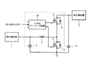
図1には、昇降圧型DC−DCコンバータの基本回路構成例が示されている。この図1において、昇圧チョッパ回路11及び降圧チョッパ回路12は、エネルギ蓄積及び放出用のリアクトル13を共用した形態となっている。具体的には、昇圧チョッパ回路11は、リアクトル13の他に、パワーMOSFET14(昇圧用スイッチング素子に相当)、ダイオード15(第1のフリーホイールダイオードに相当)、平滑用コンデンサ16を備えた構成とされ、降圧チョッパ回路12は、リアクトル13の他に、パワーMOSFET17(降圧用スイッチング素子に相当)、ダイオード18(第2のフリーホイールダイオードに相当)、平滑用コンデンサ19を備えた構成とされている。
【0015】
この場合、MOSFET14及び17は、負荷である高圧側回路20(例えば車両走行用モータを駆動するためのインバータ回路)の入力端子とグランド端子とに間に、MOSFET14が下アームとなるハーフブリッジ回路を構成するように直列接続されており、各MOSFET14及び17には、それらと並列にダイオード18及び15がそれぞれ接続される。また、リアクトル13は、直流電源である低圧側回路21(例えば車載バッテリ)の出力端子とMOSFET14及び17の共通接続点との間に接続される。さらに、平滑用コンデンサ16は、高圧側回路20の出力端子とグランド端子との間に接続され、平滑用コンデンサ19は、低圧側回路21の出力端子とグランド端子との間に接続される。
【0016】
ゼロクロス検出部22(ゼロクロス検出手段に相当)は、MOSFET14及び17の共通接続点の電圧を測定するように設けられており、昇圧チョッパ回路11及び降圧チョッパ回路12の各動作時においてリアクトル13の両端電圧が零になるタイミング毎にゼロクロス信号を発生してパルス幅演算部23(動作制御手段に相当)に与える構成となっている。
【0017】
パルス幅演算部23は、低圧側回路21の出力を昇圧する際には、昇圧チョッパ回路11で必要な出力を、外部からの出力指令信号による出力指令値などに基づいて算出すると共に、その算出結果に応じたパルス幅の第1の駆動パルスをタイマ回路などの利用により発生し、その駆動パルスを前記ゼロクロス検出部22からゼロクロス信号が出力される毎にMOSFET14に与えてこれをオンさせる動作を行う。この場合、パルス幅演算部23は、上記第1の駆動パルスのパルス幅を出力指令値に比例した大きさに設定する構成となっており、また、出力の過不足に対処するために必要に応じて当該第1の駆動パルスのパルス幅を補正する構成となっている。
【0018】
これにより、MOSFET14は、リアクトル13に流れる電流が止まる毎に第1の駆動パルスのパルス幅に応じた時間だけオンされることになる。そして、このようなオン期間には、低圧側回路21からリアクトル13に電流が供給され、その後におけるMOSFET14のオフ期間においてリアクトル13に蓄積されたエネルギに応じた電流がダイオード15を通じて平滑用コンデンサ16に流れ込むようになり、上記のようなMOSFET14のオンオフが繰り返されるに応じて周知の昇圧チョッパ機能が働くものである。
【0019】
図2(a)には、昇圧動作時において出力指令値が例えば3段階に切換えられた各状態時にリアクトル13に流れる電流の波形が模式的に示されている。この図2(a)から理解できるように、リアクトル電流は三角波状を呈するものであり、そのリアクトル電流の増減周期、つまりMOSFET14の駆動周波数は、出力の増大に比例して低下することになる。因みに、図2(b)には、図4に示した従来のPWM制御方式のDC−DCコンバータにおいて、出力が3段階に切換えられた各状態時にリアクトル7に流れる電流の波形が模式的に示されている。この図2(b)から理解できるように、PWM制御方式のDC−DCコンバータでは、リアクトル電流の増減周期(つまり、PWM信号の周期)が一定値に固定された状態となるように制御されるものである。
【0020】
尚、パルス幅演算部23は、高圧側回路20からの回生出力を降圧する際には、降圧チョッパ回路12で必要な出力電圧を、外部からの出力指令信号による出力指令値などに基づいて算出すると共に、その算出結果に応じたパルス幅の第2の駆動パルスをタイマ回路などの利用により発生し、その駆動パルスを前記ゼロクロス検出部22からゼロクロス信号が出力される毎にMOSFET17に与えてこれをオンさせる動作を行うものであり、これに伴いMOSFET17のオンオフが繰り返されるに応じて周知の降圧チョッパ機能が働くものである。
【0021】
上記した本実施例によれば、以下に述べるような作用・効果を奏することができる。尚、図3には、本実施例のような制御(これをゼロクロス制御と呼ぶ)が行われたときの出力の大きさとパルス幅演算部23から出力される駆動パルスのパルス幅及び駆動周波数との関係が実線で示されており、また、従来のPWM制御が行われたときの出力の大きさとPWM信号のパルス幅及び駆動周波数との関係が点線で示されている。
【0022】
即ち、本実施例の構成によれば、出力がある程度立ち上がった状態では、出力の大きさと、MOSFET14及び17をスイッチングするための各駆動パルスのパルス幅との関係が、図3に示すように単純な比例関係となり、しかも当該駆動パルスの決定時に出力情報のフィードバックが基本的に不要になるという特徴がある。このため、出力制御時においては、単純な演算で駆動パルスを決定できるため、制御精度及び応答性の向上を容易に実現できる。
【0023】
このような出力制御に必要となるゼロクロス検出部22は、リアクトル13に流れる電流が止まった瞬間を検出するだけで良いものであって電流値を測定する必要がないため、簡単な回路構成で済む。また、パルス幅演算部23も、単純な比例演算を行うだけで良いから簡単な回路構成で済むものであり、従って、全体の回路構成を簡単化できてコストの低減を実現できるようになる。因みに、図4に示した従来のPWM制御方式のDC−DCコンバータでは、図3に破線で示すように、パルス幅(周期)が固定された状態のPWM信号によって出力を幅広く制御する関係上、微妙なフィードバックが要求されるものであり、安定した出力を得るためには、PWM信号のパルス幅を微妙に調整するという複雑な制御が必要になり、これに対処するためには、高精度で応答性に優れた制御を行う複雑な構成の回路が必要となってコストが高騰することになる。
【0024】
本実施例によれば、上述のように制御動作時の応答性が良好であるから、例えば、昇圧動作状態から降圧動作状態への急な変更に対処するために、降圧動作用のMOSFET17を予め駆動しておくという従来構成のような非効率な制御を行う必要がなくなる。
【0025】
また、本実施例によれば、MOSFET14及び17のオンタイミングが、リアクトル電流が零になったタイミングとなるように制御される構成となっているから、MOSFET14及び17がターンオンする際にリカバリロスが発生することがなくなり、それらMOSFET14及び17として定格の小さなものを使用すれば済むようになる。しかも、このようにリカバリロスが発生しないので、MOSFET14及び17のスイッチング動作に伴う電磁波ノイズの発生も抑制できるようになる。因みに、図4に示した従来のPWM制御方式のDC−DCコンバータでは、MOSFET3及び4のスイッチング動作をリアクトル電流が流れている状態で行っているので、それらMOSFET3及び4のターンオン時には、ダイオード5或いは6を通じて数十〜数百ナノ秒オーダーのリカバリ電流が過渡的に流れる。このため、MOSFET3及び4として、不要なリカバリ損失による耐量を確保するために定格に余裕がある大型のものを使用する必要が出てくると共に、リカバリ電流が流れるのに伴い電磁波ノイズが発生するという問題点があった。
【0026】
本実施例によれば、出力の設定を、電流を計測せずに駆動パルスのパルス幅で設定するという開ループ制御可能であるから、ステップ応答出力制御、定電力量制御などを容易に行うことができる。因みに、図4に示した従来のPWM制御方式のDC−DCコンバータでは、基本的に各相の電流を計測することが不可欠であって閉ループでの微妙な制御が必要になるため、ステップ応答出力制御、定電力量制御などを行う際には良好な過渡応答特性が要求されるなど、その実現に大きな困難を伴うことになる。
【0027】
本実施例によれば、図3に示すように、出力がある程度立ち上がった状態では、出力の増大に比例してMOSFET14及び17の駆動周波数が低下するという動作特性があるため、出力増大に伴い負荷電流が増大するのに連れてMOSFET14及び17のスイッチング回数が減少することになる。つまり、出力の増大によりMOSFET14及び17の1回のスイッチング当たりの損失が増えるのに応じて、そのスイッチング回数が減少することになるから、MOSFET14及び17で発生するスイッチングロスは、軽負荷時から最大出力時までの全域にわたってほぼ一定になる。このため、MOSFET14及び17を効率的に利用できるようになり、これらに必要な素子仕様を引き下げた無駄のない設計が可能になる。因みに、図4に示した従来のPWM制御方式のDC−DCコンバータでは、図3に示すように、出力の大小と関係なく駆動周波数がほぼ一定であるため、出力の増大に連れてMOSFET3及び4でのスイッチングロスが増えるという事情がある。このため、最大出力時に合わせた素子仕様とする必要があり、定格時や軽負荷時にはオーバースペックとなるという無駄が出てくる。
【0028】
本実施例によれば、定格時や軽負荷時においてMOSFET14及び17の駆動周波数が相対的に高くなるため、最も使用頻度が高い範囲において可聴音を抑制した構成を容易に実現できる。この場合、出力が増大するのに連れて駆動周波数が低くなるため、これがユーザに聞こえることになるが、本実施例のDC−DCコンバータように車両走行用のモータを駆動するために用いられる場合には、その出力増大に応じて音が大きくなる状態が、ごく自然な状態であると広く認知されているから、ユーザに違和感を与える恐れがなくなる。これに対して、図4に示した従来のPWM制御方式のDC−DCコンバータでは、常に一定周波数の駆動音が発生することになるため、ユーザに違和感を与える恐れがあり、また、これに対処するために駆動周波数が可聴帯域に入らない構成とする場合には、駆動周波数の増大に伴うスイッチングロスの増加といった種々の障害を乗り越えなければならない。
【0029】
本実施例においては、出力指示信号による出力指令値を電力値とする構成を容易に実現できる。即ち、本実施例によれば、駆動パルスの幅を入力電圧に基づいて調整することにより出力電力値をとに基づいてきわめて容易に設定できるから、出力電流値を測定する必要がなくなるなど、回路構成が複雑化する恐れがなくなる。因みに、図4に示した従来のPWM制御方式のDC−DCコンバータでは、出力電圧値の制御を行う場合には、出力電流及び電圧を測定値に基いた計算結果によるフィードバック制御による出力補正動作が必要となり、その実現が非常に困難になる。
【0030】
(他の実施の形態)
その他、本発明は上記した実施例に限定されるものではなく、以下に述べるような変形或いは拡張が可能である。
複数組の昇圧チョッパ回路及び各降圧チョッパ回路をそれぞれ並列接続した状態で設けることにより多相化することにより、出力電流のリップル低減を図っても良い。この場合には、パルス幅演算部23は、低圧側回路21の出力を昇圧する際には、第1の駆動パルスに基づいてそれぞれ位相が異なる複数の第1の多重動作用駆動パルスを生成し、各多重動作用駆動パルスにより複数の昇圧チョッパ回路内の昇圧用スイッチング素子(MOSFET14)を個別にオンさせ、また、高圧側回路20の出力を降圧する際には、第2の駆動パルスに基づいてそれぞれ位相が異なる複数の第2の多重動作用駆動パルスを生成し、各多重動作用駆動パルスにより複数の降圧チョッパ回路内の降圧用スイッチング素子(MOSFET17)を個別にオンさせる動作を行えば良い。
【0031】
この構成によれば、一相分の第1及び第2の駆動パルスに基づいて他相のための駆動パルスを容易に生成できると共に、それらの駆動パルスに基づいた開ループ制御を行うだけで済むから、回路構成の複雑化を招くことがなくなる。因みに、図4に示した従来のPWM制御方式のDC−DCコンバータでは、その多相化が極めて困難であるため、リップル電流の低減のために多相化を図ることは一般的ではない。
【0032】
昇圧チョッパ回路11及び降圧チョッパ回路12でリアクトル13を共用する形態としたが、各チョッパ回路11及び12に専用のリアクトルを設けても良い。昇圧用及び降圧用のスイッチング素子の例としてパワーMOSFETを挙げたが、IGBTなどの他の半導体スイッチング素子であっても良い。
【図面の簡単な説明】
【図1】本発明の一実施例を示す電気的構成図
【図2】リアクトル電流波形の一例を示す図
【図3】出力の大きさと駆動パルスのパルス幅及び駆動周波数との関係を示す特性図
【図4】従来構成を示す図1相当図
【符号の説明】
11は昇圧チョッパ回路、12は降圧チョッパ回路、13はリアクトル、14はパワーMOSFET(昇圧用スイッチング素子)、15はダイオード(第1のフリーホイールダイオード)、16は平滑用コンデンサ、17はパワーMOSFET(降圧用スイッチング素子)、18はダイオード(第2のフリーホイールダイオード)、19は平滑用コンデンサ、20は高圧側回路(負荷)、21は低圧側回路(直流電源)、22はゼロクロス検出部(ゼロクロス検出手段)、23はパルス幅演算部(動作制御手段)を示す。[0001]
TECHNICAL FIELD OF THE INVENTION
The present invention relates to a step-up / step-down DC-DC converter including a step-up chopper circuit and a step-down chopper circuit.
[0002]
[Problems to be solved by the invention]
For example, in an electric vehicle, a hybrid vehicle, or the like, a control is performed in which a DC-DC converter is provided in front of an inverter circuit for driving a traveling motor, and the converter boosts a battery voltage and supplies the boosted battery voltage to the inverter circuit. ing. Further, when the traveling motor enters a regenerative state, the regenerative power is stepped down by the DC-DC converter and used for charging the battery. Conventionally, a PWM control type DC-DC converter is generally used as such a step-up / step-down DC-DC converter.
[0003]
FIG. 4 shows a basic circuit configuration example of such a step-up / step-down DC-DC converter. In FIG. 4, a
[0004]
A reactor 7 for energy storage and release is connected between the low
[0005]
When performing a boosting operation, the
[0006]
With such a circuit configuration, a PWM control system including a boost chopper circuit including the
[0007]
In the DC-DC converter having the above-described conventional configuration, it is indispensable to feed back the output voltage in order to generate the PWM signal. However, since the output must be widely controlled by the PWM signal having a fixed period, the feedback is required. There is a situation that the gain is high. Therefore, in order to obtain a stable output, complicated control for finely adjusting the pulse width of the PWM signal is required, and there is a problem that the control becomes extremely difficult. In order to achieve this, a circuit having a complicated configuration that performs control with high accuracy and excellent responsiveness is required, which causes a problem that the cost increases.
[0008]
In addition, the current control has a problem that the response is poor, so that inefficient control is required. Specifically, for example, during the step-up operation, it is not necessary to drive the MOSFET 4 constituting the step-down chopper circuit, but in order to cope with such a sudden change from the step-up operation state to the step-down operation state, Since sufficient responsiveness cannot be expected with this control method, inefficient control of driving the MOSFET 4 which is not required to be driven is performed.
[0009]
In addition, since the response to the control operation is poor, the output voltage tends to fluctuate. For this reason, it is necessary to take measures such as increasing the capacity of the capacitors 8 and 9. This also has a problem that it becomes an obstacle in reducing the size of the device.
[0010]
SUMMARY OF THE INVENTION The present invention has been made to solve the above problems, and an object of the present invention is to provide a DC-DC converter exhibiting an effect of enabling stable output control with a simple circuit configuration. It is in.
[0011]
[Means for Solving the Problems]
According to the first aspect of the present invention, the zero-crossing detecting means generates a zero-crossing signal each time the voltage across the reactor becomes zero during each operation of the step-up chopper circuit and the step-down chopper circuit. The operation control means generates a first drive pulse having a pulse width proportional to an output command value based on an output instruction signal for the boost chopper circuit, and the drive pulse is generated every time the zero-cross signal is output. An operation of giving a boost switching element in the circuit to turn it on, and generating a second drive pulse having a pulse width proportional to an output command value by an output instruction signal for the step-down chopper circuit, Each time a zero-cross signal is output, it is supplied to a step-down switching element in a step-down chopper circuit to turn on the switching element.
[0012]
In this case, the relationship between the magnitude of the output and the pulse width of each drive pulse for turning on the step-up and step-down switching elements has a simple proportional relationship, and the feedback of the output information is fundamental when the drive pulse is determined. Is no longer necessary. For this reason, at the time of the output control, the drive pulse can be determined by a simple calculation, and the control accuracy and the response can be easily improved. The zero-crossing detecting means required for such output control only needs to detect the moment when the current flowing through the reactor stops, and does not need to measure the current value, so that a simple circuit configuration is sufficient. Also, the operation control means only needs to perform a simple proportional operation, so that a simple circuit configuration is sufficient. Therefore, the overall circuit configuration can be simplified and the cost can be reduced.
[0013]
According to the second aspect, a plurality of sets of the step-up chopper circuits and the step-down chopper circuits are connected in parallel to form a multi-phase, so that the ripple of the output current can be reduced. In this case, drive pulses for the other phases can be easily generated based on the drive pulses for one phase, and open-loop control based on those drive pulses only needs to be performed, resulting in a complicated circuit configuration. Will not be.
[0014]
BEST MODE FOR CARRYING OUT THE INVENTION
Hereinafter, an embodiment in which the present invention is applied to a vehicle-mounted DC-DC converter will be described with reference to FIGS.
FIG. 1 shows an example of a basic circuit configuration of a step-up / step-down DC-DC converter. In FIG. 1, the step-up chopper circuit 11 and the step-down chopper circuit 12 share a reactor 13 for storing and discharging energy. Specifically, the boost chopper circuit 11 includes a power MOSFET 14 (corresponding to a boost switching element), a diode 15 (corresponding to a first freewheel diode), and a
[0015]
In this case, the
[0016]
The zero-cross detector 22 (corresponding to a zero-cross detector) is provided so as to measure the voltage at the common connection point between the
[0017]
When boosting the output of the low-voltage side circuit 21, the pulse width calculation unit 23 calculates an output required by the boost chopper circuit 11 based on an output command value based on an external output command signal, and the like. An operation of generating a first drive pulse having a pulse width corresponding to the result by using a timer circuit or the like, applying the drive pulse to the
[0018]
Thus, the
[0019]
FIG. 2A schematically shows a waveform of a current flowing through the reactor 13 in each state in which the output command value is switched to, for example, three stages during the boosting operation. As can be understood from FIG. 2A, the reactor current has a triangular waveform, and the increase / decrease cycle of the reactor current, that is, the drive frequency of the
[0020]
When the regenerative output from the high voltage side circuit 20 is stepped down, the pulse width calculation unit 23 calculates an output voltage required by the step-down chopper circuit 12 based on an output command value based on an external output command signal or the like. At the same time, a second drive pulse having a pulse width corresponding to the calculation result is generated by using a timer circuit or the like, and the drive pulse is supplied to the
[0021]
According to the above-described embodiment, the following operations and effects can be obtained. FIG. 3 shows the magnitude of the output, the pulse width and the driving frequency of the driving pulse output from the pulse width calculating unit 23 when the control as in the present embodiment (this is called zero-crossing control) is performed. Is shown by a solid line, and the relationship between the magnitude of the output and the pulse width and the driving frequency of the PWM signal when the conventional PWM control is performed is shown by a dotted line.
[0022]
That is, according to the configuration of the present embodiment, when the output rises to some extent, the relationship between the magnitude of the output and the pulse width of each driving pulse for switching the
[0023]
The zero-crossing detector 22 required for such output control only needs to detect the moment when the current flowing through the reactor 13 stops and does not need to measure the current value, so that a simple circuit configuration is sufficient. . In addition, the pulse width calculation unit 23 also requires only a simple proportional calculation, and therefore requires only a simple circuit configuration. Therefore, the overall circuit configuration can be simplified and the cost can be reduced. Incidentally, in the conventional DC-DC converter of the PWM control method shown in FIG. 4, as shown by a broken line in FIG. 3, since the output is widely controlled by the PWM signal having a fixed pulse width (period), A delicate feedback is required, and in order to obtain a stable output, a complicated control of finely adjusting the pulse width of the PWM signal is required. A circuit having a complicated configuration for performing control with excellent responsiveness is required, and the cost rises.
[0024]
According to the present embodiment, since the response during the control operation is good as described above, for example, in order to cope with a sudden change from the step-up operation state to the step-down operation state, the step-down
[0025]
Further, according to the present embodiment, since the on-timing of the
[0026]
According to the present embodiment, the output can be set by the pulse width of the drive pulse without measuring the current, so that open-loop control is possible, so that step response output control, constant power control, and the like can be easily performed. Can be. Incidentally, in the conventional PWM control type DC-DC converter shown in FIG. 4, it is basically essential to measure the current of each phase, and delicate control in a closed loop is required. When performing control, constant power control, and the like, a good transient response characteristic is required, and there is a great difficulty in realizing this.
[0027]
According to the present embodiment, as shown in FIG. 3, when the output has risen to some extent, the driving frequency of the
[0028]
According to the present embodiment, the drive frequency of the
[0029]
In this embodiment, it is possible to easily realize a configuration in which the output command value based on the output command signal is used as the power value. That is, according to the present embodiment, since the output power value can be set very easily based on the input voltage by adjusting the width of the drive pulse, it is not necessary to measure the output current value. There is no fear that the configuration is complicated. By the way, in the conventional PWM control type DC-DC converter shown in FIG. 4, when controlling the output voltage value, the output correction operation by the feedback control based on the calculation result based on the measured values of the output current and the voltage is performed. Required and very difficult to achieve.
[0030]
(Other embodiments)
In addition, the present invention is not limited to the above-described embodiment, and can be modified or expanded as described below.
By providing a plurality of sets of the step-up chopper circuits and the step-down chopper circuits in a state of being connected in parallel with each other to make the phases multi-phase, the ripple of the output current may be reduced. In this case, when boosting the output of the low-voltage side circuit 21, the pulse width calculation unit 23 generates a plurality of first multiplex operation drive pulses having different phases based on the first drive pulse. When the boosting switching elements (MOSFETs 14) in the plurality of boosting chopper circuits are individually turned on by each multiplex operation drive pulse, and when the output of the high-voltage side circuit 20 is stepped down, it is determined based on the second drive pulse. A plurality of second multiplex operation drive pulses having different phases from each other may be generated, and an operation of individually turning on the step-down switching elements (MOSFETs 17) in the plurality of step-down chopper circuits may be performed by each multiplex operation drive pulse. .
[0031]
According to this configuration, drive pulses for other phases can be easily generated based on the first and second drive pulses for one phase, and it is only necessary to perform open-loop control based on those drive pulses. Therefore, the circuit configuration does not become complicated. Incidentally, in the conventional PWM control type DC-DC converter shown in FIG. 4, it is extremely difficult to increase the number of phases, so that it is not general to increase the number of phases to reduce the ripple current.
[0032]
Although the reactor 13 is shared by the step-up chopper circuit 11 and the step-down chopper circuit 12, a dedicated reactor may be provided for each of the chopper circuits 11 and 12. Although a power MOSFET has been described as an example of the switching element for step-up and step-down, another semiconductor switching element such as an IGBT may be used.
[Brief description of the drawings]
FIG. 1 is an electrical configuration diagram showing one embodiment of the present invention. FIG. 2 is a diagram showing an example of a reactor current waveform. FIG. 3 is a characteristic showing a relationship between an output magnitude, a pulse width of a driving pulse, and a driving frequency. FIG. 4 is a diagram corresponding to FIG. 1 showing a conventional configuration.
11 is a step-up chopper circuit, 12 is a step-down chopper circuit, 13 is a reactor, 14 is a power MOSFET (step-up switching element), 15 is a diode (first freewheel diode), 16 is a smoothing capacitor, and 17 is a power MOSFET ( Step-down switching element), 18 is a diode (second freewheeling diode), 19 is a smoothing capacitor, 20 is a high-voltage side circuit (load), 21 is a low-voltage side circuit (DC power supply), and 22 is a zero-crossing detector (zero-crossing). Reference numeral 23 denotes a pulse width calculation unit (operation control unit).
Claims (2)
前記昇圧チョッパ回路及び降圧チョッパ回路の各動作時において前記リアクトルの両端電圧が零になるタイミング毎にゼロクロス信号を発生するゼロクロス検出手段と、
前記昇圧チョッパ回路のための出力指示信号による出力指令値に比例したパルス幅の第1の駆動パルスを発生すると共に、その駆動パルスを前記ゼロクロス信号が出力される毎に前記昇圧用スイッチング素子に与えてこれをオンさせる動作、並びに前記降圧チョッパ回路のための出力指示信号による出力指令値に比例したパルス幅の第2の駆動パルスを発生すると共に、その駆動パルスを前記ゼロクロス信号が出力される毎に前記降圧用スイッチング素子に与えてこれをオンさせる動作を行う動作制御手段とを備えたことを特徴とするDC−DCコンバータ。A step-up chopper circuit for boosting a DC power supply output using a reactor, a first freewheel diode and a boosting switching element and applying the boosted chopper circuit to a load; DC-DC converter configured in combination with a step-down chopper circuit that provides a step-down voltage to the DC power supply using a switching element for
Zero cross detection means for generating a zero cross signal each time the voltage across the reactor becomes zero during each operation of the step-up chopper circuit and the step-down chopper circuit,
A first drive pulse having a pulse width proportional to an output command value based on an output command signal for the boost chopper circuit is generated, and the drive pulse is supplied to the boost switching element every time the zero-cross signal is output. To generate a second drive pulse having a pulse width proportional to an output command value based on an output command signal for the step-down chopper circuit, and to change the drive pulse every time the zero-cross signal is output. A DC-DC converter characterized by further comprising an operation control means for giving an operation to the step-down switching element to turn it on.
前記動作制御手段は、前記第1の駆動パルスに基づいてそれぞれ位相が異なる複数の第1の多重動作用駆動パルスを生成し、各多重動作用駆動パルスにより前記複数の昇圧チョッパ回路内の昇圧用スイッチング素子を個別にオンさせると共に、前記第2の駆動パルスに基づいてそれぞれ位相が異なる複数の第2の多重動作用駆動パルスを生成し、各多重動作用駆動パルスにより前記複数の降圧チョッパ回路内の降圧用スイッチング素子を個別にオンさせる動作を行うことを特徴とする請求項1記載のDC−DCコンバータ。While adding at least one set of the step-up chopper circuit and the step-down chopper circuit, and connecting each step-up chopper circuit and each step-down chopper circuit in parallel, polyphase is achieved,
The operation control means generates a plurality of first multiplex operation drive pulses having different phases based on the first drive pulse, and generates a plurality of boost operation signals in the plurality of boost chopper circuits by each multiplex operation drive pulse. The switching elements are individually turned on, and a plurality of second multiplex operation drive pulses having different phases are generated based on the second drive pulse, and the plurality of multiplex operation drive pulses are used in the plurality of step-down chopper circuits. 2. The DC-DC converter according to claim 1, wherein an operation of individually turning on the step-down switching elements is performed.
Priority Applications (1)
| Application Number | Priority Date | Filing Date | Title |
|---|---|---|---|
| JP2003068086A JP4107113B2 (en) | 2003-03-13 | 2003-03-13 | DC-DC converter |
Applications Claiming Priority (1)
| Application Number | Priority Date | Filing Date | Title |
|---|---|---|---|
| JP2003068086A JP4107113B2 (en) | 2003-03-13 | 2003-03-13 | DC-DC converter |
Publications (2)
| Publication Number | Publication Date |
|---|---|
| JP2004282835A true JP2004282835A (en) | 2004-10-07 |
| JP4107113B2 JP4107113B2 (en) | 2008-06-25 |
Family
ID=33285519
Family Applications (1)
| Application Number | Title | Priority Date | Filing Date |
|---|---|---|---|
| JP2003068086A Expired - Lifetime JP4107113B2 (en) | 2003-03-13 | 2003-03-13 | DC-DC converter |
Country Status (1)
| Country | Link |
|---|---|
| JP (1) | JP4107113B2 (en) |
Cited By (7)
| Publication number | Priority date | Publication date | Assignee | Title |
|---|---|---|---|---|
| JP2007116846A (en) * | 2005-10-21 | 2007-05-10 | Fujitsu Ten Ltd | Switching regulator |
| JP2008067472A (en) * | 2006-09-06 | 2008-03-21 | Toyota Motor Corp | Dc-dc converter and control method therefor |
| US7576521B2 (en) | 2006-03-16 | 2009-08-18 | Fujitsu Ten Limited | Switching regulator |
| KR101031068B1 (en) | 2006-06-01 | 2011-04-25 | 도요타 지도샤(주) | Power supply device and its control method |
| US9381875B2 (en) | 2013-04-02 | 2016-07-05 | Denso Corporation | Power supply control apparatus |
| WO2016188300A1 (en) * | 2015-10-22 | 2016-12-01 | 中兴通讯股份有限公司 | Buck-topology-based switch power supply control circuit and solar controller |
| US11658557B2 (en) | 2020-08-25 | 2023-05-23 | Toyota Jidosha Kabushiki Kaisha | Control device and control method |
-
2003
- 2003-03-13 JP JP2003068086A patent/JP4107113B2/en not_active Expired - Lifetime
Cited By (8)
| Publication number | Priority date | Publication date | Assignee | Title |
|---|---|---|---|---|
| JP2007116846A (en) * | 2005-10-21 | 2007-05-10 | Fujitsu Ten Ltd | Switching regulator |
| US7576521B2 (en) | 2006-03-16 | 2009-08-18 | Fujitsu Ten Limited | Switching regulator |
| KR101031068B1 (en) | 2006-06-01 | 2011-04-25 | 도요타 지도샤(주) | Power supply device and its control method |
| JP2008067472A (en) * | 2006-09-06 | 2008-03-21 | Toyota Motor Corp | Dc-dc converter and control method therefor |
| JP4609400B2 (en) * | 2006-09-06 | 2011-01-12 | トヨタ自動車株式会社 | DC-DC converter and control method thereof |
| US9381875B2 (en) | 2013-04-02 | 2016-07-05 | Denso Corporation | Power supply control apparatus |
| WO2016188300A1 (en) * | 2015-10-22 | 2016-12-01 | 中兴通讯股份有限公司 | Buck-topology-based switch power supply control circuit and solar controller |
| US11658557B2 (en) | 2020-08-25 | 2023-05-23 | Toyota Jidosha Kabushiki Kaisha | Control device and control method |
Also Published As
| Publication number | Publication date |
|---|---|
| JP4107113B2 (en) | 2008-06-25 |
Similar Documents
| Publication | Publication Date | Title |
|---|---|---|
| KR101514914B1 (en) | Power supply system | |
| JP4196867B2 (en) | Bidirectional buck-boost chopper circuit, inverter circuit using the same, and DC-DC converter circuit | |
| JP4640200B2 (en) | Voltage conversion device and voltage converter control method | |
| JP4280573B2 (en) | Load drive device | |
| JP4110470B2 (en) | Multiphase multiple control system | |
| JP6269647B2 (en) | Power system | |
| JP6153144B1 (en) | Control device and control method for DC / DC converter | |
| US20120229061A1 (en) | Voltage converter and voltage converter system including voltage converter | |
| JP2000083374A (en) | Switching regulator | |
| JP6185860B2 (en) | Bidirectional converter | |
| JP2010220443A (en) | Vehicle mounted multiphase converter | |
| JP2009273280A (en) | Dc-dc converter | |
| JP5927217B2 (en) | Power system | |
| JP6702209B2 (en) | Power converter | |
| JP5288178B2 (en) | Motor drive system | |
| JP6065753B2 (en) | DC / DC converter and battery charge / discharge device | |
| JP2008154377A (en) | Multiphase dc-dc converter and control method for multiphase dc-dc converter | |
| JP4107113B2 (en) | DC-DC converter | |
| JP2004166370A (en) | Voltage converter | |
| US10135327B2 (en) | Power supply system | |
| US20230031930A1 (en) | Dual-purpose drive and charger systems and methods thereof | |
| JP5122200B2 (en) | Drive controller for buck-boost converter and buck-boost converter | |
| JP2020089024A (en) | Electric vehicle | |
| JP7188355B2 (en) | electric vehicle motor drive | |
| JP2004201400A (en) | Reactor device |
Legal Events
| Date | Code | Title | Description |
|---|---|---|---|
| A621 | Written request for application examination |
Free format text: JAPANESE INTERMEDIATE CODE: A621 Effective date: 20050418 |
|
| A977 | Report on retrieval |
Free format text: JAPANESE INTERMEDIATE CODE: A971007 Effective date: 20070816 |
|
| A131 | Notification of reasons for refusal |
Free format text: JAPANESE INTERMEDIATE CODE: A131 Effective date: 20070911 |
|
| TRDD | Decision of grant or rejection written | ||
| A01 | Written decision to grant a patent or to grant a registration (utility model) |
Free format text: JAPANESE INTERMEDIATE CODE: A01 Effective date: 20080311 |
|
| A61 | First payment of annual fees (during grant procedure) |
Free format text: JAPANESE INTERMEDIATE CODE: A61 Effective date: 20080324 |
|
| FPAY | Renewal fee payment (event date is renewal date of database) |
Free format text: PAYMENT UNTIL: 20110411 Year of fee payment: 3 |
|
| R150 | Certificate of patent or registration of utility model |
Ref document number: 4107113 Country of ref document: JP Free format text: JAPANESE INTERMEDIATE CODE: R150 Free format text: JAPANESE INTERMEDIATE CODE: R150 |
|
| FPAY | Renewal fee payment (event date is renewal date of database) |
Free format text: PAYMENT UNTIL: 20120411 Year of fee payment: 4 |
|
| FPAY | Renewal fee payment (event date is renewal date of database) |
Free format text: PAYMENT UNTIL: 20120411 Year of fee payment: 4 |
|
| FPAY | Renewal fee payment (event date is renewal date of database) |
Free format text: PAYMENT UNTIL: 20130411 Year of fee payment: 5 |
|
| FPAY | Renewal fee payment (event date is renewal date of database) |
Free format text: PAYMENT UNTIL: 20130411 Year of fee payment: 5 |
|
| FPAY | Renewal fee payment (event date is renewal date of database) |
Free format text: PAYMENT UNTIL: 20140411 Year of fee payment: 6 |
|
| R250 | Receipt of annual fees |
Free format text: JAPANESE INTERMEDIATE CODE: R250 |
|
| R250 | Receipt of annual fees |
Free format text: JAPANESE INTERMEDIATE CODE: R250 |
|
| R250 | Receipt of annual fees |
Free format text: JAPANESE INTERMEDIATE CODE: R250 |
|
| R250 | Receipt of annual fees |
Free format text: JAPANESE INTERMEDIATE CODE: R250 |
|
| R250 | Receipt of annual fees |
Free format text: JAPANESE INTERMEDIATE CODE: R250 |
|
| R250 | Receipt of annual fees |
Free format text: JAPANESE INTERMEDIATE CODE: R250 |
|
| R250 | Receipt of annual fees |
Free format text: JAPANESE INTERMEDIATE CODE: R250 |
|
| R250 | Receipt of annual fees |
Free format text: JAPANESE INTERMEDIATE CODE: R250 |
|
| R250 | Receipt of annual fees |
Free format text: JAPANESE INTERMEDIATE CODE: R250 |
|
| EXPY | Cancellation because of completion of term |