JP2004228085A - Positioning method of deposition material correctly to channel of channel plate and switch manufactured using above method - Google Patents
Positioning method of deposition material correctly to channel of channel plate and switch manufactured using above method Download PDFInfo
- Publication number
- JP2004228085A JP2004228085A JP2004010695A JP2004010695A JP2004228085A JP 2004228085 A JP2004228085 A JP 2004228085A JP 2004010695 A JP2004010695 A JP 2004010695A JP 2004010695 A JP2004010695 A JP 2004010695A JP 2004228085 A JP2004228085 A JP 2004228085A
- Authority
- JP
- Japan
- Prior art keywords
- channel plate
- channel
- resist
- channels
- switch
- Prior art date
- Legal status (The legal status is an assumption and is not a legal conclusion. Google has not performed a legal analysis and makes no representation as to the accuracy of the status listed.)
- Pending
Links
Images


Classifications
-
- B—PERFORMING OPERATIONS; TRANSPORTING
- B81—MICROSTRUCTURAL TECHNOLOGY
- B81C—PROCESSES OR APPARATUS SPECIALLY ADAPTED FOR THE MANUFACTURE OR TREATMENT OF MICROSTRUCTURAL DEVICES OR SYSTEMS
- B81C1/00—Manufacture or treatment of devices or systems in or on a substrate
- B81C1/00436—Shaping materials, i.e. techniques for structuring the substrate or the layers on the substrate
- B81C1/00555—Achieving a desired geometry, i.e. controlling etch rates, anisotropy or selectivity
- B81C1/00611—Processes for the planarisation of structures
-
- H—ELECTRICITY
- H01—ELECTRIC ELEMENTS
- H01H—ELECTRIC SWITCHES; RELAYS; SELECTORS; EMERGENCY PROTECTIVE DEVICES
- H01H1/00—Contacts
- H01H1/0036—Switches making use of microelectromechanical systems [MEMS]
-
- H—ELECTRICITY
- H01—ELECTRIC ELEMENTS
- H01H—ELECTRIC SWITCHES; RELAYS; SELECTORS; EMERGENCY PROTECTIVE DEVICES
- H01H11/00—Apparatus or processes specially adapted for the manufacture of electric switches
-
- H—ELECTRICITY
- H01—ELECTRIC ELEMENTS
- H01H—ELECTRIC SWITCHES; RELAYS; SELECTORS; EMERGENCY PROTECTIVE DEVICES
- H01H11/00—Apparatus or processes specially adapted for the manufacture of electric switches
- H01H11/02—Apparatus or processes specially adapted for the manufacture of electric switches for mercury switches
-
- H—ELECTRICITY
- H01—ELECTRIC ELEMENTS
- H01H—ELECTRIC SWITCHES; RELAYS; SELECTORS; EMERGENCY PROTECTIVE DEVICES
- H01H29/00—Switches having at least one liquid contact
-
- H—ELECTRICITY
- H01—ELECTRIC ELEMENTS
- H01H—ELECTRIC SWITCHES; RELAYS; SELECTORS; EMERGENCY PROTECTIVE DEVICES
- H01H29/00—Switches having at least one liquid contact
- H01H29/28—Switches having at least one liquid contact with level of surface of contact liquid displaced by fluid pressure
-
- B—PERFORMING OPERATIONS; TRANSPORTING
- B81—MICROSTRUCTURAL TECHNOLOGY
- B81B—MICROSTRUCTURAL DEVICES OR SYSTEMS, e.g. MICROMECHANICAL DEVICES
- B81B2201/00—Specific applications of microelectromechanical systems
- B81B2201/01—Switches
- B81B2201/012—Switches characterised by the shape
- B81B2201/018—Switches not provided for in B81B2201/014 - B81B2201/016
-
- B—PERFORMING OPERATIONS; TRANSPORTING
- B81—MICROSTRUCTURAL TECHNOLOGY
- B81C—PROCESSES OR APPARATUS SPECIALLY ADAPTED FOR THE MANUFACTURE OR TREATMENT OF MICROSTRUCTURAL DEVICES OR SYSTEMS
- B81C2201/00—Manufacture or treatment of microstructural devices or systems
- B81C2201/01—Manufacture or treatment of microstructural devices or systems in or on a substrate
- B81C2201/0101—Shaping material; Structuring the bulk substrate or layers on the substrate; Film patterning
- B81C2201/0118—Processes for the planarization of structures
- B81C2201/0121—Processes for the planarization of structures involving addition of material followed by removal of parts of said material, i.e. subtractive planarization
-
- H—ELECTRICITY
- H01—ELECTRIC ELEMENTS
- H01H—ELECTRIC SWITCHES; RELAYS; SELECTORS; EMERGENCY PROTECTIVE DEVICES
- H01H29/00—Switches having at least one liquid contact
- H01H2029/008—Switches having at least one liquid contact using micromechanics, e.g. micromechanical liquid contact switches or [LIMMS]
Abstract
Description
本発明は、堆積材料をチャネルプレートのチャネルに正確に位置合わせする方法、及びこの方法を使用して製造されたスイッチに関するものである。 The present invention relates to a method for accurately aligning a deposited material with the channels of a channel plate, and to a switch manufactured using this method.
以下の特許文献1、およびMarvin Glenn Wongによる米国特許出願である、「ピエゾ駆動方式の液体金属スイッチ(A Piezoelectrically Actuated Liquid Metal Switch)」(出願番号:10/137,691、2002年5月2日出願)および「スイッチ用レーザ・カット・チャネル・プレート(Laser Cut Channel Plate for a Switch)」(出願番号:10/317,932、2002年12月12日出願)には、液体金属マイクロスイッチ(Liquid Metal Micro Switch:LIMMS)などの、流体ベースのスイッチが開示されている(本引用により、これらの開示内容は本明細書に包含される)。 U.S. Patent Application Publication No. US 2005/0128300 and US Patent Application by Marvin Glenn Wong, "A Piezoelectrically Actuated Liquid Metal Switch" (Application No. 10/137, 691, May 2, 2002). Application) and “Laser Cut Channel Plate for a Switch” (application number: 10 / 317,932, filed on December 12, 2002) include a liquid metal microswitch (Liquid). Fluid-based switches, such as Metal Micro Switch (LIMMS), are disclosed (the disclosures of which are incorporated herein by reference).
これらの特許文献及び特許出願に開示されているスイッチを製造する方法の1つは、(1)チャネルプレート上に粘着物を堆積した後に、(2)チャネルプレートと基板の間に、スイッチング流体、作動流体、及び/又はその他のスイッチコンポーネントの所望の組み合わせを封入する方法である。
通常、チャネルプレート上に粘着物を堆積する際には、チャネルプレートのチャネルに対して粘着物を正確に「位置合わせ」することが望ましい。即ち、チャネルプレートのチャネルのところまで正確に粘着物が延在するように(但し、チャネル内部には侵入しないように)、チャネルプレート上に粘着物を堆積することが望ましい。これにより、チャネルプレートを基板に封着した際に、チャネルによって定義される空洞の容積が粘着物(の位置合わせ誤差)によって増加又は減少することを回避することができる。 Normally, when depositing an adhesive on a channel plate, it is desirable to accurately "align" the adhesive with the channels of the channel plate. That is, it is desirable to deposit the adhesive on the channel plate so that the adhesive extends exactly to the channel of the channel plate (but does not enter the inside of the channel). Thus, when the channel plate is sealed to the substrate, it is possible to prevent the volume of the cavity defined by the channel from increasing or decreasing due to (adjustment error of the adhesive).
本発明の一態様は、チャネルプレート内に形成された1つ又は複数のチャネルに対して材料が正確に位置合わせされるように、材料をチャネルプレート上に堆積する方法として実施される。この方法は、(1)堆積材料によって湿潤することのないレジストを複数のチャネルの中の少なくとも1つに充填する段階と、(2)チャネルプレート中の少なくとも1つの領域上であって、少なくともレジストの一部と境を接する部分に堆積材料を堆積する段階と、(3)レジストを除去する段階と、を有している。 One aspect of the present invention is implemented as a method of depositing material on a channel plate such that the material is accurately aligned with one or more channels formed in the channel plate. The method comprises: (1) filling at least one of the plurality of channels with a resist that is not wetted by the deposited material; and (2) at least one region on the channel plate, wherein the resist is And (3) removing the resist.
本発明の別の態様は、(1)チャネルプレート内に少なくとも1つのチャネルを形成する段階と、(2)複数のチャネルの中の少なくとも1つに、チャネルプレートに堆積する堆積材料によって湿潤することのないレジストを充填する段階と、(3)チャネルプレート中の少なくとも1つの領域上であって、レジストの一部と少なくとも境を接する部分に堆積材料を堆積する段階と、(4)レジストを除去する段階と、(5)チャネルプレート内に形成された少なくとも1つのチャネルを基板上の少なくとも1つの特徴部分とアライメントし、堆積材料により、チャネルプレートと基板間に、少なくともスイッチング流体を封入する段階と、によって製造されるスイッチとして実施される。 Another aspect of the invention involves (1) forming at least one channel in the channel plate, and (2) wetting at least one of the plurality of channels with a deposition material that is deposited on the channel plate. (3) depositing a deposition material on at least one region in the channel plate and at least bordering a portion of the resist; and (4) removing the resist. (5) aligning at least one channel formed in the channel plate with at least one feature on the substrate, and encapsulating at least a switching fluid between the channel plate and the substrate with the deposited material. , Implemented as a switch.
チャネルプレート上に堆積材料を堆積(デポジット、塗布、成膜)する際に、チャネルプレート内に形成された1つ又は複数のチャネルに対して材料を正確に位置合わせすることが望ましい場合がある。即ち、材料がチャネルプレートのチャネルのところまで延在するように(但し、チャネル内部には延在しないように)、チャネルプレート上に材料を堆積することが望ましい場合がある。 When depositing (depositing, applying, depositing) a deposition material on a channel plate, it may be desirable to accurately align the material with one or more channels formed in the channel plate. That is, it may be desirable to deposit the material on the channel plate such that the material extends to the channels of the channel plate, but not into the channels.
流体ベースのスイッチは、チャネルに対して堆積材料を正確に位置合わせすることが望ましいアプリケーションの1つである。例えば、本明細書の「背景技術」で開示した特許及び特許出願に従ってスイッチを製造する際には、チャネルプレートを基板に封着するべくチャネルプレートに粘着物を塗布する。これらチャネルプレート及び基板の間には、スイッチング流体、作動流体、及び/又はその他のスイッチコンポーネントが封入される。通常、チャネルプレートに粘着物を堆積する際には、チャネルプレートを基板に封着した際にチャネルによって定義される空洞の容積が粘着物によって増加又は減少しないように、チャネルプレートのチャネルに対して粘着物を正確に位置合わせすることが望ましい。 Fluid-based switches are one application in which it is desirable to accurately align the deposited material with the channel. For example, when manufacturing a switch in accordance with the patents and patent applications disclosed in the “Background of the Invention” section, an adhesive is applied to the channel plate to seal the channel plate to a substrate. Switching fluid, working fluid, and / or other switch components are encapsulated between the channel plate and the substrate. Usually, when depositing the sticky substance on the channel plate, the channel plate channel is sealed against the channel so that the volume of the cavity defined by the channel when the channel plate is sealed to the substrate is not increased or decreased by the sticky substance. It is desirable to accurately align the adhesive.
チャネルプレートのチャネルに対して粘着物を正確に位置合わせする方法の1つは、チャネルプレート上に粘着物の層を堆積し、これを部分的に硬化(半硬化)させ、次いで、粘着物上にフォトレジストの層を堆積し、このフォトレジスト層を光学的にパターニングした後に、サンド・ブラストによってチャネルプレートから粘着物を除去する方法である。しかしながら、このプロセスは、例えば、(1)チャネルに対する粘着物の位置合わせの公差が相対的に大きく、且つ、(2)サンド・ブラストの結果、生成されるチャネルの表面が粗くなる、という欠点を有している。又、このプロセスの場合には、チャネルプレートに使用可能な基板のタイプが制限されると共に、形成可能なチャネル構造の形状も制限されている。 One method of accurately aligning the adhesive to the channels of the channel plate is to deposit a layer of adhesive on the channel plate, partially cure (semi-cur), and then Is a method of depositing a photoresist layer on the substrate, optically patterning the photoresist layer, and then removing the adhesive from the channel plate by sand blasting. However, this process has the disadvantage, for example, that (1) the tolerance of alignment of the adhesive to the channel is relatively large, and (2) the surface of the resulting channel is roughened as a result of sand blasting. Have. In addition, in this process, the types of substrates that can be used for the channel plate are limited, and the shape of the channel structure that can be formed is also limited.
従って、本発明者らは、チャネルプレート上に材料を堆積する新しい方法、並びにこの方法に従って製造される新しいスイッチを発明した。この新しい方法によれば、チャネルプレート内に形成された1つの又は複数のチャネルに対して堆積材料をより正確に位置合わせすることができる。 Accordingly, the inventors have invented a new method of depositing material on a channel plate, as well as a new switch manufactured according to this method. With this new method, the deposited material can be more accurately aligned with one or more channels formed in the channel plate.
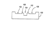
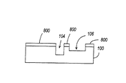
図1〜図3は、チャネルプレート100の第1の実施の形態を例示している。図1は、チャネルプレート100の平面図を示しており、図2及び図3は、チャネルプレート100の断面を2つ例示している。このようなチャネルプレートは、例えば、LIMMSなどの流体ベースのスイッチに使用可能である。一例として、チャネルプレート100は、深さの異なる5つの異なるチャネル102、104、106、108、110を有するものとして示されているが、チャネルプレートを使用するスイッチの構成に応じて、これよりも多くの/又は少ない数のチャネルをチャネルプレート内に形成することが予見される。このチャネルプレート100用の基材としては、例えば、ガラス、セラミック、金属、又は重合体であってよい。使用する基材と所望のチャネル公差に応じて、機械加工、射出成型、プレス成型、スランプ成型(slump mold)、エッチング、レーザーカット、超音波加工、張り合わせ(積層)、圧造(あるいはプレス)、又はその他の方法でチャネルプレート100内にチャネルを形成可能である。
1 to 3 illustrate a first embodiment of the
本明細書における「チャネル」という用語は、チャネルプレートの上部表面下に延在するチャネルプレート内部の凹部を形成するあらゆる種類の溝、トラフ、窪み、又はその他の特徴部分として定義されるものである。 As used herein, the term "channel" is defined as any type of groove, trough, depression, or other feature that forms a recess within a channel plate that extends below the top surface of the channel plate. .
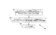
本発明に従い、図4には、堆積材料がチャネルプレート100内に形成された1つ又は複数のチャネル102〜110に対して正確に位置合わせされるように、チャネルプレート100上に材料を堆積する方法400が示されている。この方法400は、チャネルプレート100上に、堆積する材料によって湿潤することのないレジストをチャネルプレートのチャネル102〜110の中の少なくとも1つに充填する段階402を有している。通常、チャネルプレートのチャネル102〜110のすべてにレジストを充填するものと予見されるが、チャネルプレートの複数のチャネルの中の一部を堆積材料で充填又は被覆することが望ましいアプリケーションも存在する。このようなアプリケーションでは、堆積材料で充填又は被覆することになるチャネルには、レジストは充填されない。
In accordance with the present invention, FIG. 4 illustrates depositing material on
チャネル104、106には、例えば、図5又は図6に示されているように、レジスト500を充填することができる。図5においては、レジスト500は、チャネルプレートのチャネル104、106にのみ堆積されている。この代わりに、図6に示されているように、レジスト500がチャネルプレートのチャネル104、106の境界を越えて延在するように、レジスト500をチャネルプレート100の表面全体に堆積することも可能である。図6に示されているようにレジスト500を堆積した場合には、図4に示す方法の次の段階へ進む前に、チャネルプレートのチャネル104、106の外に位置しているレジスト500の部分を除去する必要があるが、図6に示されているレジスト500の堆積方法は、図5に示されているレジスト500の堆積方法に比べ、容易であり、且つ迅速であろう。
The
チャネルプレート100に対するレジスト500の堆積方法とは関係なく、チャネルプレート100を研磨してレジスト500をチャネルプレート100の表面と同一平面にすること(即ち、レジスト500と、このレジスト500が充填されているチャネル104、106の端部との間の変わり目をより明確にすること)が望ましい。この研磨後には、図5及び図6に示されているレジスト500を有するチャネルプレート100は、図7に示されているようになる。
Regardless of the method of depositing the
一例として、チャネルプレート100は、化学機械的平坦化法、又は研削及び研磨処理によって研磨することができる。
As an example, the
過剰なレジスト500を除去することのみを目的としてチャネルプレート100を研磨してもよいが、レジストが充填されたチャネル104、106を有するチャネルプレートの1つ又は複数の表面を平坦化することを目的としてチャネルプレート100を研磨してもよい。チャネルプレート100上に堆積する材料が粘着物又はガスケット材料である場合には、チャネルプレート100を平坦化することにより、後工程においてチャネルプレート100を合体させる部分に対するチャネルプレート100の接合(即ち、適合)状態が良好なものになる。
The
1つ又は複数のチャネル104、106にレジスト500を充填した後に、チャネルプレート100の少なくとも1つの領域で、少なくともレジスト500の一部と境を接する部分上に所望の材料800を堆積する(図4の404)(図8を参照されたい)。換言すれば、材料800は、チャネルプレートの表面全体にわたって堆積する必要はなく、又、チャネルプレート100上で、レジストを充填したチャネル104を全部囲繞するような領域にわたって堆積する必要もない。即ち、例えば、材料800は、レジスト500を充填したチャネル104の一端を含む領域112を堆積するか(図1を参照されたい)、或いは、レジスト500を充填したチャネル104の一側114、116を、主に堆積するのである。この代わりに、チャネルプレートの複数表面中の1つ又は複数のものの全体にわたって材料800を堆積してもよい。
After the one or
一例として、材料層800は、スピンコーティング法又はスプレーコーティング法によってチャネルプレート100上に堆積することができる。チャネルプレート100上に堆積する材料800によって湿潤することのないようにレジスト500が選択されているため、更には、堆積材料の表面張力によって、堆積材料800が延在する範囲は、レジスト500の境界までに限定される。従って、レジスト500がチャネルプレートのチャネル104、106の境界に対して正確に位置合わせされていれば、堆積材料800もチャネル104、106の境界に対して正確に位置合わせされることになる。
As an example, the
図9は、チャネルプレート100のチャネル104の境界における堆積材料800の角900、902に丸みの付く様子を示している。この効果は、堆積材料800の厚さが増大するほど顕著になる。必要な場合には、堆積材料800を研磨し、丸みの存在する材料部分を除去することも可能である。
FIG. 9 shows that the
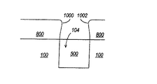
図10には、チャネルプレート100上に堆積した材料層800が厚過ぎる場合に発生する望ましくない影響が示されている。図10に示されているように、材料層800は、厚過ぎると、チャネルプレートのチャネル104上に「傾斜」することになる。この場合にも、堆積材料800を研磨し、過剰に傾斜した材料部分を除去することができる。或いは、この代わりに、より薄い層の材料800をチャネルプレート100上に堆積してもよい。
FIG. 10 illustrates the undesired effects that occur when the
材料800の堆積が完了すれば、レジスト500を除去することができる(406)(図11を参照されたい)。一例として、レジスト500は、エッチング又は現像プロセスを使用して除去可能である。堆積材料800の特性とレジスト500の除去に使用するプロセスに応じて、レジスト500を除去する前に、堆積材料800の硬化が必要になる場合がある。この硬化は、一定時間にわたって堆積材料800を外部環境に露出させたり、堆積材料800を加熱したり、堆積材料800を適切な溶液中に浸漬したり、或いはその他の手段によって実現することができる。必要に応じて、レジスト500を除去した後に、堆積材料800を硬化(或いは、更に硬化)させることも可能である。
Once the deposition of the
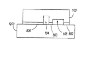
必要に応じて、堆積材料800を有するチャネルプレート100を別の部分(部品)と合体させることができる(例えば、堆積材料800が粘着物又はガスケットである流体に基づいたスイッチの場合には、このチャネルプレート100を合体させる対象となる部分は、スイッチ基板1200である(図12))。
If desired, the
次に、流体ベースのスイッチの製造が図4の方法を適用する1つの可能な選択肢であり意図するアプリケーションである場合の、図4の方法を適用可能ないくつかの模範的な流体ベースのスイッチについて説明する。 Next, some exemplary fluid-based switches applicable to the method of FIG. 4 where the manufacture of the fluid-based switch is one possible option and intended application of applying the method of FIG. Will be described.
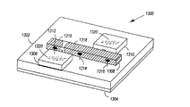
図13は、スイッチ1300の第1の実施の形態を例示している。このスイッチ1300は、いくつかの空洞1306、1308、1310の少なくとも一部を定義するチャネルプレート1302を有している。空洞1306〜1310の残りの部分(存在する場合)は、チャネルプレート1302を封着する対象の基板1304によって定義可能である。複数の空洞の中の1つ又は複数のものの内部に露出されているのは、複数の電極1312、1314、1316である。複数の空洞の中の1つ又は複数のものの内部に保持されているスイッチング流体1318(例:水銀などの導電性の液体金属)は、それに加えられる力に応答し、複数の電極1312〜1316の中の少なくとも1つのペアを開閉するべく機能する。複数の空洞の中の1つ又は複数のものの内部に保持されている作動流体1320(例:不活性ガス又は液体)は、スイッチング流体1318に力を加えるべく機能する。
FIG. 13 illustrates a first embodiment of the
スイッチ1300の一実施例においては、このスイッチング流体1318に加えられる力は、作動流体1320における圧力変化の結果、生成される。作動流体1320における圧力の変化により、スイッチング流体1318に圧力の変化が生じ、この結果、スイッチング流体1318の形状の変化、移動、分割などが発生するのである。図13においては、空洞1306内に保持されている作動流体1320の圧力により、図示のごとく、スイッチング流体1318を分割するべく力が加えられている。この状態では、スイッチ1300の右側の電極のペア1314、1316が相互接続されている。一方、空洞1306内に保持されている作動流体1320の圧力が解除され、空洞1310内に保持されている作動流体1320の圧力が増大すると、電極1314及び1316の接続が解除され、電極1312及び1314が接続されるように、分割及び合体させるための力がスイッチング流体1318に加えられる。
In one embodiment of
一例として、この作動流体1320における圧力変化は、作動流体1320の加熱、又は圧電ポンピングを利用することによって実現可能である。前者については、Kondoh他による「電気接点ブレーカスイッチ、一体型電気接点ブレーカスイッチ、及び電気接点スイッチング法(Electrical Contact Breaker Switch、 Integrated Electrical Contact Breaker Switch、 and Electrical Contact Switching Method)」という名称の米国特許第6,323,447号に開示されている。後者については、Marvin Glenn Wongによる「ピエゾ駆動方式の液体金属スイッチ(A Piezoelectrically Actuated Liquid Metal Switch)」という名称の2002年5月2日付けの米国特許出願第10/137,691号の明細書に記述されている。これらの特許及び特許出願には、デュアルプッシュ/プル作動流体空洞によるスイッチング流体の移動が開示されているが、スイッチング流体に対して空洞から十分に大きなプッシュ/プルの圧力変化が付与される場合には、シングルプッシュ/プル作動流体空洞で十分であろう。このような構成の場合には、本明細書において開示しているチャネルプレート100と同様に、スイッチ用のチャネルプレートを構築可能である。
As an example, the pressure change in the working
スイッチ1300のチャネルプレート1302は、図1〜図3に示されているように、内部に形成された複数のチャネル102〜110を備えることができる。スイッチ1300の一実施例においては、チャネルプレート100(又は1302)内の第1チャネル104は、スイッチング流体1318を保持する1つ又は複数の空洞1308の少なくとも一部を定義している。一例として、このスイッチング流体チャネル104は、幅が約200ミクロン、長さが約2600ミクロン、深さが約200ミクロンである。
The
作動流体1320を保持する1つ又は複数の空洞1306、1310の少なくとも一部を定義するべく、チャネルプレート100(又は、1302)内に、1つの第2チャネル(又は、複数の第2チャネル102、106)を形成することができる。一例として、これらの作動流体チャネル102、106は、それぞれ、幅が約350ミクロン、長さが約1400ミクロン、深さが約300ミクロンである。
Within the channel plate 100 (or 1302), a second channel (or a plurality of
スイッチング流体及び作動流体1318、1320を保持する空洞1306〜1310を接続する1つ又は複数の空洞の少なくとも一部を定義するべく、チャネルプレート100(又は、1302)内に、1つの第3チャネル(又は、複数の第3チャネル108、110)を形成することができる。一例として、作動流体チャネル102、106をスイッチング流体チャネル104に接続するチャネル108、110は、それぞれ、幅が約100ミクロン、長さが約600ミクロン、深さが約130ミクロンである。
One third channel (or channel) in the channel plate 100 (or 1302) to define at least a portion of one or more cavities connecting the cavities 1306-1310 holding the switching and working
図14には、図13に示されているスイッチ1300を製造する方法の例1400が示されている。この方法1400は、チャネルプレート100(又は、1302)内に少なくとも1つのチャネル102〜110を形成する段階1402から始まっている。次いで、複数のチャネルの中の少なくとも1つ104に、チャネルプレート100上に堆積する材料800によって湿潤することのないレジスト500を充填する(1404)。その後、チャネルプレート100上の少なくとも1つの領域であって、レジスト500の一部と少なくとも境を接する領域上に、材料800を堆積する(1406)。この材料800は、様々な方法によって堆積可能であり、これには、例えば、スピンコーティング法やスプレーコーティング法が含まれる。
FIG. 14 shows an example 1400 of a method of manufacturing the
材料800を堆積した後に、レジスト500を除去する(1408)。任意選択により、レジスト500を除去する前に、堆積材料800を硬化させることも可能である。そして、最後に、チャネルプレート100(又は、1302)内に形成された少なくとも1つのチャネル102〜110を基板1304上の少なくとも1つの特徴部分とアライメントし、堆積された材料800により、チャネルプレート1302と基板1304間に、少なくともスイッチング流体1318を封入する(1410)。図13に開示されているように、チャネルプレート1302と基板1304間に作動流体1320を封入することも可能である。
After depositing the
チャネルプレート1302上に堆積する材料800は、例えば、粘着物又はガスケット材料であってよい。好適な粘着物の1つがCytop(登録商標)である(日本の東京に所在する旭硝子株式会社の製品である)。Cytopは、アプリケーションに応じて2つの異なる接着促進剤パッケージと共に提供される。チャネルプレート100が無機組成を備えている場合には、Cytopの無機接着促進剤を使用すると共に、有機レジスト500を使用するべきである。同様に、チャネルプレート100が有機組成を備えている場合には、Cytopの有機接着促進剤を使用すると共に、無機レジスト500を使用するべきである(これには、金属又はガラスの薄膜スパッタリングコーティングなどの無機レジストが含まれる)。
The
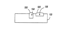
任意選択により、図15及び図16に示されているように、「シールベルト」1502、1504、1506を生成するべく、チャネルプレート100(又は、1302)の一部に(例えば、シャドーマスクを介したスパッタリング又は蒸着、或いはフォトレジストを介したエッチングによって)金属を被覆することも可能である。シールベルト1502〜1506は、チャネルプレート100上に粘着物又はガスケット材料を堆積する前後において生成可能である。スイッチング流体チャネル104の内部にシールベルト1502〜1506を生成することにより、スイッチング流体が湿潤可能な追加表面領域が提供される。これは、スイッチング流体が設定可能な様々な状態への切り替えのみならず、スイッチング流体の散逸を防止し(スイッチの状態が変化する際に)スイッチング流体のポンピングが容易に行われる密閉チャンバの生成にも有用である。
Optionally, as shown in FIGS. 15 and 16, a portion of the channel plate 100 (or 1302) (eg, via a shadow mask) to create “seal belts” 1502, 1504, 1506. It is also possible to coat the metal (by sputtering or evaporation, or by etching through a photoresist).
図13に示されているものなどのスイッチの構造と動作の更なる詳細については、前述のKondoh他による特許とMarvin Wongによる特許出願を参照されたい。 For further details of the structure and operation of switches such as those shown in FIG. 13, see the aforementioned Kondoh et al. Patent and the Marvin Wong patent application.
図17は、スイッチ1700の第2の実施の形態を例示している。このスイッチ1700は、いくつかの空洞1706、1708、1710の少なくとも一部を定義するチャネルプレート1702を有している。空洞1706〜1710の残りの部分(存在する場合)は、チャネルプレート1702を封着する対象の基板1704によって定義可能である。複数の空洞の中の1つ又は複数のものの内部に露出しているのは、複数の湿潤可能なパッド1712〜1716である。スイッチング流体1718(例:水銀などの液体金属)は、パッド1712〜1716を湿潤可能であり、複数の空洞の中の1つ又は複数のものの内部に保持されている。スイッチング流体1718は、それに印加される力に応答し、複数の空洞の中の1つ又は複数のものを貫通する光の経路1722/1724、1726/1728を開放及び遮断するべく機能する。一例として、この光の経路は、スイッチング流体を保持する空洞1708内の光を透過するウィンドウにアライメントされた導波路1722〜1728によって定義することができる。この光の経路1722/1724、1726/1728の遮断は、不透明のスイッチング流体1718によって実現可能である。複数の空洞の中の1つ又は複数のものの内部に保持された作動流体1720(例:不活性ガス又は液体)は、スイッチング流体1718に力を印加するべく機能する。
FIG. 17 illustrates a second embodiment of the
これらの力は、図13のスイッチング流体及び作動流体1318、1320に加えるのと同様に、スイッチング及び作動流体1718、1720に対して加えることが可能である。
These forces can be applied to the switching and working
スイッチ1700のチャネルプレート1702は、図1〜図3に示されているように、内部に形成された複数のチャネル102〜110を備えることができる。スイッチ1700の一実施例においては、チャネルプレート100(又は、1702)内の第1チャネル104は、スイッチング流体1718を保持する1つ又は複数の空洞1708の一部を定義している。
The
作動流体1720を保持する1つ又は複数の空洞1706、1710の少なくとも一部を定義するべく、チャネルプレート100(又は、1702)内に、1つの第2チャネル(又は、複数の第2チャネル102、106)を形成することができる。
Within the channel plate 100 (or 1702), a second channel (or a plurality of
スイッチング及び作動流体1718、1720を保持する空洞1706〜1710を接続する1つ又は複数の空洞の少なくとも一部を定義するべく、チャネルプレート100(又は1702)内に、1つの第3チャネル(又は、複数の第3チャネル108、110)を形成することができる。
One third channel (or, in the channel plate 100 (or 1702)) defines at least a portion of one or more cavities connecting the cavities 1706-1710 holding the switching and working
図17に示されているものなどのスイッチの構造と動作の更なる詳細については、前述のコンドウ他による特許とマービン・ウォンによる特許出願を参照されたい。又、このスイッチのチャネルプレート1702には、前述のごとく、図14〜図16に示されているように、粘着物又はガスケット層、並びにシールベルトを堆積可能である。
For further details of the structure and operation of switches such as those shown in FIG. 17, see the aforementioned Kondo et al. Patent and the Marvin Wong patent application. As described above, the adhesive or gasket layer and the seal belt can be deposited on the
このチャネルプレートの用途は、図13及び図17に開示されているスイッチ1300、1700に限定されるものではなく、例えば、(1)複数の空洞の少なくとも一部を定義するチャネルプレート(その第1空洞は、チャネルプレート内の超音波加工されたチャネルによって定義されている)と、(2)複数の空洞の中の1つ又は複数のものの内部に保持され、スイッチング流体に印加される力に応答し、少なくとも第1及び第2スイッチ状態間で移動可能なスイッチング流体と、を有するその他の形態のスイッチにおいても実施可能である。
The application of the channel plate is not limited to the
以上、本発明を例証する現時点における好適な実施例について詳細に説明したが、本発明の概念は、これら以外にも様々に実施及び使用可能であり、従来技術によって制限されるものを除き、それらの変形も添付の特許請求の範囲に属するものと解釈されることを理解されたい。 Although the presently preferred embodiments illustrating the present invention have been described in detail, the concept of the present invention can be variously implemented and used in addition to the above, except for those limited by the prior art. It is to be understood that modifications of the above may be construed as belonging to the appended claims.
なお、本発明は例として次の態様を含む。( )内の数字は添付図面の参照符号に対応する。
[1] スイッチ(1300)であって、
(a)チャネルプレート(100)内に少なくとも1つのチャネル(102、104、106)を形成すること(1402)と、
(b)前記チャネルプレート上に堆積する堆積材料(800)によって湿潤することのないレジスト(500)を前記チャネルの中の少なくとも1つ(104)に充填すること(1404)と、
(c)前記チャネルプレート上の少なくとも1つの領域であって、前記レジストの一部と少なくとも境を接する領域上に前記堆積材料を堆積すること(1406)と、
(d)前記レジストを除去すること(1408)と、
(e)前記チャネルプレート内に形成された少なくとも1つのチャネルを基板(1200)上の少なくとも1つの特徴部分とアライメントし、前記堆積材料により、前記チャネルプレートと前記基板間に少なくともスイッチング流体(1318)を封入すること(1410)と、
によって製造されることを特徴とするスイッチ。
[2] (a)前記チャネルプレート内に形成された前記少なくとも1つのチャネル(102、104、106)は、前記スイッチング流体(1318)を保持するチャネル(104)と、作動流体(1320)を保持する一対のチャネル(102、106)と、前記作動流体を保持する前記チャネルの中の対応するものを前記スイッチング流体を保持する前記チャネルに接続する一対のチャネル(108、110)と、を有し、
(b)前記チャネルのすべてに前記レジスト(500)が充填される、
ことを特徴とする上記[1]に記載のスイッチ(1300)。
[3] チャネルプレート(100)内に形成された1つ又は複数のチャネル(104、106)に対して堆積材料が正確に位置合わせされるように、前記チャネルプレート(100)上に前記堆積材料(800)を堆積する方法(400)であって、
(a)前記堆積材料によって湿潤することのないレジスト(500)を前記チャネルの中の少なくとも1つ(104)に充填すること(402)と、
(b)前記チャネルプレートの少なくとも1つの領域であって、前記レジストの一部と少なくとも境を接する領域上に前記堆積材料を堆積すること(404)と、
(c)前記レジストを除去すること(406)と、
を有することを特徴とする方法。
[4] 前記堆積材料(800)は粘着物であることを特徴とする上記[3]に記載の方法(400)。
[5] 前記レジスト(500)を除去することの前に、前記粘着物(800)を硬化させることを更に有することを特徴とする上記[4]に記載の方法(400)。
[6] 前記堆積材料(800)が、スピンコーティング法によって堆積されることを特徴とする上記[3]に記載の方法(400)。
[7] 前記堆積材料(800)は、スプレーコーティング法によって堆積されることを特徴とする上記[3]に記載の方法(400)。
[8] 前記レジスト(500)は、エッチング法によって除去されることを特徴とする上記[3]に記載の方法(400)。
[9] 前記レジスト(500)は、現像によって除去されることを特徴とする上記[3]に記載の方法(400)。
[10] 前記レジスト(500)を前記少なくとも1つのチャネル(104)に充填した後に、前記チャネルプレート(100)を研磨し、前記レジストと、前記レジストが充填された前記チャネルの端部との間の変わり目を明確にすることを更に有する特徴とする上記[3]に記載の方法(400)。
The present invention includes the following aspects as examples. The numbers in parentheses correspond to the reference numerals in the attached drawings.
[1] A switch (1300),
(A) forming (1402) at least one channel (102, 104, 106) in the channel plate (100);
(B) filling at least one (104) of the channels with a resist (500) that is not wettable by a deposition material (800) deposited on the channel plate (1404);
(C) depositing the deposition material on at least one region on the channel plate that is at least bounded by a portion of the resist (1406);
(D) removing the resist (1408);
(E) aligning at least one channel formed in the channel plate with at least one feature on a substrate (1200), wherein the deposition material causes at least a switching fluid (1318) between the channel plate and the substrate. Enclosing (1410)
A switch characterized by being manufactured by:
[2] (a) The at least one channel (102, 104, 106) formed in the channel plate holds a channel (104) holding the switching fluid (1318) and a working fluid (1320). And a pair of channels (108, 110) connecting the corresponding one of the channels holding the working fluid to the channel holding the switching fluid. ,
(B) filling all of the channels with the resist (500);
The switch (1300) according to the above [1], characterized in that:
[3] The deposition material on the channel plate (100) such that the deposition material is accurately aligned with one or more channels (104, 106) formed in the channel plate (100). A method (400) for depositing (800), comprising:
(A) filling at least one (104) of the channels (402) with a resist (500) that is not wettable by the deposition material;
(B) depositing the deposition material on at least one region of the channel plate that at least borders a portion of the resist;
(C) removing the resist (406);
A method comprising:
[4] The method (400) according to the above [3], wherein the deposition material (800) is an adhesive.
[5] The method (400) according to the above [4], further comprising curing the adhesive (800) before removing the resist (500).
[6] The method (400) according to the above [3], wherein the deposition material (800) is deposited by a spin coating method.
[7] The method (400) according to the above [3], wherein the deposition material (800) is deposited by a spray coating method.
[8] The method (400) according to the above [3], wherein the resist (500) is removed by an etching method.
[9] The method (400) according to the above [3], wherein the resist (500) is removed by development.
[10] After filling the at least one channel (104) with the resist (500), the channel plate (100) is polished so that a gap between the resist and an end of the channel filled with the resist is formed. The method (400) according to the above [3], further characterized by clarifying the transition of:
100、1302、1702 チャネルプレート
102、104、106、108、110 チャネル
500 レジスト
800 材料(堆積材料)
1200 スイッチ基板
1300、1700 スイッチ
1306、1308、1310 空洞
1312、1314、1316 電極
1318 スイッチング流体
1320 作動流体
1706、1708、1710 空洞
1712,1714、1716 パッド
100, 1302, 1702
1200
Claims (1)
(a)チャネルプレート内に少なくとも1つのチャネルを形成することと、
(b)前記チャネルプレート上に堆積する堆積材料によって湿潤することのないレジストを前記チャネルの中の少なくとも1つに充填することと、
(c)前記チャネルプレート上の少なくとも1つの領域であって、前記レジストの一部と少なくとも境を接する領域上に前記堆積材料を堆積することと、
(d)前記レジストを除去することと、
(e)前記チャネルプレート内に形成された少なくとも1つのチャネルを基板上の少なくとも1つの特徴部分とアライメントし、前記堆積材料により、前記チャネルプレートと前記基板間に少なくともスイッチング流体を封入することと、
によって製造されることを特徴とするスイッチ。 A switch,
(A) forming at least one channel in the channel plate;
(B) filling at least one of the channels with a resist that is not wetted by a deposition material deposited on the channel plate;
(C) depositing the deposition material on at least one region on the channel plate that at least borders a portion of the resist;
(D) removing the resist;
(E) aligning at least one channel formed in the channel plate with at least one feature on a substrate, and enclosing at least a switching fluid between the channel plate and the substrate with the deposition material;
A switch characterized by being manufactured by:
Applications Claiming Priority (1)
| Application Number | Priority Date | Filing Date | Title |
|---|---|---|---|
| US10/349,712 US6809277B2 (en) | 2003-01-22 | 2003-01-22 | Method for registering a deposited material with channel plate channels, and switch produced using same |
Publications (2)
| Publication Number | Publication Date |
|---|---|
| JP2004228085A true JP2004228085A (en) | 2004-08-12 |
| JP2004228085A5 JP2004228085A5 (en) | 2007-02-22 |
Family
ID=31715575
Family Applications (1)
| Application Number | Title | Priority Date | Filing Date |
|---|---|---|---|
| JP2004010695A Pending JP2004228085A (en) | 2003-01-22 | 2004-01-19 | Positioning method of deposition material correctly to channel of channel plate and switch manufactured using above method |
Country Status (5)
| Country | Link |
|---|---|
| US (2) | US6809277B2 (en) |
| JP (1) | JP2004228085A (en) |
| DE (1) | DE10344571A1 (en) |
| GB (1) | GB2397695B (en) |
| TW (1) | TW200414251A (en) |
Families Citing this family (24)
| Publication number | Priority date | Publication date | Assignee | Title |
|---|---|---|---|---|
| US6855898B2 (en) | 2002-12-12 | 2005-02-15 | Agilent Technologies, Inc. | Ceramic channel plate for a switch |
| US7070908B2 (en) | 2003-04-14 | 2006-07-04 | Agilent Technologies, Inc. | Feature formation in thick-film inks |
| WO2009135115A1 (en) * | 2008-05-01 | 2009-11-05 | The Govt. Of The U.S.A. As Represented By The Secretary Of The Navy Naval Research Laboratory | Microfabricated gas chromatograph |
| KR102423377B1 (en) | 2013-08-05 | 2022-07-25 | 트위스트 바이오사이언스 코포레이션 | De novo synthesized gene libraries |
| CA2975855A1 (en) | 2015-02-04 | 2016-08-11 | Twist Bioscience Corporation | Compositions and methods for synthetic gene assembly |
| CA2975852A1 (en) | 2015-02-04 | 2016-08-11 | Twist Bioscience Corporation | Methods and devices for de novo oligonucleic acid assembly |
| WO2016172377A1 (en) | 2015-04-21 | 2016-10-27 | Twist Bioscience Corporation | Devices and methods for oligonucleic acid library synthesis |
| CN108368482A (en) | 2015-09-18 | 2018-08-03 | 特韦斯特生物科学公司 | Oligonucleotide Mutant libraries and its synthesis |
| WO2017053450A1 (en) | 2015-09-22 | 2017-03-30 | Twist Bioscience Corporation | Flexible substrates for nucleic acid synthesis |
| CA3006867A1 (en) | 2015-12-01 | 2017-06-08 | Twist Bioscience Corporation | Functionalized surfaces and preparation thereof |
| EP3500672A4 (en) | 2016-08-22 | 2020-05-20 | Twist Bioscience Corporation | De novo synthesized nucleic acid libraries |
| US10417457B2 (en) | 2016-09-21 | 2019-09-17 | Twist Bioscience Corporation | Nucleic acid based data storage |
| US10907274B2 (en) | 2016-12-16 | 2021-02-02 | Twist Bioscience Corporation | Variant libraries of the immunological synapse and synthesis thereof |
| CA3054303A1 (en) | 2017-02-22 | 2018-08-30 | Twist Bioscience Corporation | Nucleic acid based data storage |
| CN110913865A (en) | 2017-03-15 | 2020-03-24 | 特韦斯特生物科学公司 | Library of variants of immune synapses and synthesis thereof |
| KR102628876B1 (en) | 2017-06-12 | 2024-01-23 | 트위스트 바이오사이언스 코포레이션 | Methods for seamless nucleic acid assembly |
| WO2018231864A1 (en) | 2017-06-12 | 2018-12-20 | Twist Bioscience Corporation | Methods for seamless nucleic acid assembly |
| AU2018328847A1 (en) | 2017-09-11 | 2020-04-23 | Twist Bioscience Corporation | GPCR binding proteins and synthesis thereof |
| KR102637566B1 (en) | 2017-10-20 | 2024-02-16 | 트위스트 바이오사이언스 코포레이션 | Heated nanowells for polynucleotide synthesis |
| WO2019136175A1 (en) | 2018-01-04 | 2019-07-11 | Twist Bioscience Corporation | Dna-based digital information storage |
| EP3814497A4 (en) | 2018-05-18 | 2022-03-02 | Twist Bioscience Corporation | Polynucleotides, reagents, and methods for nucleic acid hybridization |
| SG11202109283UA (en) | 2019-02-26 | 2021-09-29 | Twist Bioscience Corp | Variant nucleic acid libraries for antibody optimization |
| EP3930753A4 (en) | 2019-02-26 | 2023-03-29 | Twist Bioscience Corporation | Variant nucleic acid libraries for glp1 receptor |
| JP2022550497A (en) | 2019-06-21 | 2022-12-02 | ツイスト バイオサイエンス コーポレーション | Barcode-based nucleic acid sequence assembly |
Family Cites Families (82)
| Publication number | Priority date | Publication date | Assignee | Title |
|---|---|---|---|---|
| US2312672A (en) * | 1941-05-09 | 1943-03-02 | Bell Telephone Labor Inc | Switching device |
| US2564081A (en) * | 1946-05-23 | 1951-08-14 | Babson Bros Co | Mercury switch |
| GB1143822A (en) * | 1965-08-20 | |||
| DE1614671B2 (en) * | 1967-12-04 | 1971-09-30 | Siemens AG, 1000 Berlin u. 8000 München | INDEPENDENT MERCURY RELAY |
| US3639165A (en) * | 1968-06-20 | 1972-02-01 | Gen Electric | Resistor thin films formed by low-pressure deposition of molybdenum and tungsten |
| US3600537A (en) * | 1969-04-15 | 1971-08-17 | Mechanical Enterprises Inc | Switch |
| US3657647A (en) * | 1970-02-10 | 1972-04-18 | Curtis Instr | Variable bore mercury microcoulometer |
| US4103135A (en) * | 1976-07-01 | 1978-07-25 | International Business Machines Corporation | Gas operated switches |
| FR2392485A1 (en) * | 1977-05-27 | 1978-12-22 | Orega Circuits & Commutation | SWITCH WITH WET CONTACTS, AND MAGNETIC CONTROL |
| SU714533A2 (en) * | 1977-09-06 | 1980-02-05 | Московский Ордена Трудового Красного Знамени Инженерно-Физический Институт | Switching device |
| FR2418539A1 (en) | 1978-02-24 | 1979-09-21 | Orega Circuits & Commutation | Liquid contact relays driven by piezoelectric membrane - pref. of polyvinylidene fluoride film for high sensitivity at low power |
| FR2458138A1 (en) | 1979-06-01 | 1980-12-26 | Socapex | RELAYS WITH WET CONTACTS AND PLANAR CIRCUIT COMPRISING SUCH A RELAY |
| US4419650A (en) * | 1979-08-23 | 1983-12-06 | Georgina Chrystall Hirtle | Liquid contact relay incorporating gas-containing finely reticular solid motor element for moving conductive liquid |
| US4245886A (en) * | 1979-09-10 | 1981-01-20 | International Business Machines Corporation | Fiber optics light switch |
| US4336570A (en) * | 1980-05-09 | 1982-06-22 | Gte Products Corporation | Radiation switch for photoflash unit |
| DE8016981U1 (en) * | 1980-06-26 | 1980-11-06 | W. Guenther Gmbh, 8500 Nuernberg | Mercury electrode switch |
| DE3138968A1 (en) * | 1981-09-30 | 1983-04-14 | Siemens AG, 1000 Berlin und 8000 München | OPTICAL CONTROL DEVICE FOR CONTROLLING THE RADIATION GUIDED IN AN OPTICAL WAVE GUIDE, IN PARTICULAR OPTICAL SWITCHES |
| DE3206919A1 (en) * | 1982-02-26 | 1983-09-15 | Philips Patentverwaltung Gmbh, 2000 Hamburg | DEVICE FOR OPTICALLY DISCONNECTING AND CONNECTING LIGHT GUIDES |
| US4475033A (en) * | 1982-03-08 | 1984-10-02 | Northern Telecom Limited | Positioning device for optical system element |
| FR2524658A1 (en) * | 1982-03-30 | 1983-10-07 | Socapex | OPTICAL SWITCH AND SWITCHING MATRIX COMPRISING SUCH SWITCHES |
| US4628161A (en) * | 1985-05-15 | 1986-12-09 | Thackrey James D | Distorted-pool mercury switch |
| GB8513542D0 (en) * | 1985-05-29 | 1985-07-03 | Gen Electric Co Plc | Fibre optic coupler |
| US4652710A (en) * | 1986-04-09 | 1987-03-24 | The United States Of America As Represented By The United States Department Of Energy | Mercury switch with non-wettable electrodes |
| JPS62276838A (en) | 1986-05-26 | 1987-12-01 | Hitachi Ltd | Semiconductor device |
| US4742263A (en) * | 1986-08-15 | 1988-05-03 | Pacific Bell | Piezoelectric switch |
| US4804932A (en) * | 1986-08-22 | 1989-02-14 | Nec Corporation | Mercury wetted contact switch |
| JPS63294317A (en) | 1987-01-26 | 1988-12-01 | Shimizu Tekkosho:Goushi | Body seal machine |
| US4797519A (en) * | 1987-04-17 | 1989-01-10 | Elenbaas George H | Mercury tilt switch and method of manufacture |
| US5278012A (en) * | 1989-03-29 | 1994-01-11 | Hitachi, Ltd. | Method for producing thin film multilayer substrate, and method and apparatus for detecting circuit conductor pattern of the substrate |
| US4988157A (en) * | 1990-03-08 | 1991-01-29 | Bell Communications Research, Inc. | Optical switch using bubbles |
| FR2667396A1 (en) | 1990-09-27 | 1992-04-03 | Inst Nat Sante Rech Med | Sensor for pressure measurement in a liquid medium |
| US5415026A (en) * | 1992-02-27 | 1995-05-16 | Ford; David | Vibration warning device including mercury wetted reed gauge switches |
| DE69220951T2 (en) | 1992-10-22 | 1998-01-15 | Ibm | Near field phatone tunnel devices |
| US5886407A (en) * | 1993-04-14 | 1999-03-23 | Frank J. Polese | Heat-dissipating package for microcircuit devices |
| US5972737A (en) * | 1993-04-14 | 1999-10-26 | Frank J. Polese | Heat-dissipating package for microcircuit devices and process for manufacture |
| GB9309327D0 (en) * | 1993-05-06 | 1993-06-23 | Smith Charles G | Bi-stable memory element |
| JP2682392B2 (en) * | 1993-09-01 | 1997-11-26 | 日本電気株式会社 | Thin film capacitor and method of manufacturing the same |
| GB9403122D0 (en) * | 1994-02-18 | 1994-04-06 | Univ Southampton | Acousto-optic device |
| JPH08125487A (en) | 1994-06-21 | 1996-05-17 | Kinseki Ltd | Piezoelectric vibrator |
| FI110727B (en) * | 1994-06-23 | 2003-03-14 | Vaisala Oyj | Electrically adjustable thermal radiation source |
| JP3182301B2 (en) * | 1994-11-07 | 2001-07-03 | キヤノン株式会社 | Microstructure and method for forming the same |
| US5675310A (en) * | 1994-12-05 | 1997-10-07 | General Electric Company | Thin film resistors on organic surfaces |
| US5502781A (en) * | 1995-01-25 | 1996-03-26 | At&T Corp. | Integrated optical devices utilizing magnetostrictively, electrostrictively or photostrictively induced stress |
| WO1996030916A2 (en) * | 1995-03-27 | 1996-10-03 | Philips Electronics N.V. | Method of manufacturing an electronic multilayer component |
| JPH08330507A (en) * | 1995-05-30 | 1996-12-13 | Motorola Inc | Hybrid multichip module and its preparation |
| US5751074A (en) * | 1995-09-08 | 1998-05-12 | Edward B. Prior & Associates | Non-metallic liquid tilt switch and circuitry |
| US5732168A (en) * | 1995-10-31 | 1998-03-24 | Hewlett Packard Company | Thermal optical switches for light |
| US6023408A (en) * | 1996-04-09 | 2000-02-08 | The Board Of Trustees Of The University Of Arkansas | Floating plate capacitor with extremely wide band low impedance |
| JP2817717B2 (en) * | 1996-07-25 | 1998-10-30 | 日本電気株式会社 | Semiconductor device and manufacturing method thereof |
| US5874770A (en) * | 1996-10-10 | 1999-02-23 | General Electric Company | Flexible interconnect film including resistor and capacitor layers |
| US5841686A (en) * | 1996-11-22 | 1998-11-24 | Ma Laboratories, Inc. | Dual-bank memory module with shared capacitors and R-C elements integrated into the module substrate |
| GB2321114B (en) * | 1997-01-10 | 2001-02-21 | Lasor Ltd | An optical modulator |
| US6180873B1 (en) * | 1997-10-02 | 2001-01-30 | Polaron Engineering Limited | Current conducting devices employing mesoscopically conductive liquids |
| TW405129B (en) * | 1997-12-19 | 2000-09-11 | Koninkl Philips Electronics Nv | Thin-film component |
| US6021048A (en) * | 1998-02-17 | 2000-02-01 | Smith; Gary W. | High speed memory module |
| US6351579B1 (en) * | 1998-02-27 | 2002-02-26 | The Regents Of The University Of California | Optical fiber switch |
| DE19910375C2 (en) | 1998-03-09 | 2001-10-04 | Bartels Mikrotechnik Gmbh | Optical switch and modular switching system made of optical switching elements |
| US6207234B1 (en) * | 1998-06-24 | 2001-03-27 | Vishay Vitramon Incorporated | Via formation for multilayer inductive devices and other devices |
| US6212308B1 (en) * | 1998-08-03 | 2001-04-03 | Agilent Technologies Inc. | Thermal optical switches for light |
| US5912606A (en) * | 1998-08-18 | 1999-06-15 | Northrop Grumman Corporation | Mercury wetted switch |
| US6323447B1 (en) * | 1998-12-30 | 2001-11-27 | Agilent Technologies, Inc. | Electrical contact breaker switch, integrated electrical contact breaker switch, and electrical contact switching method |
| EP1050773A1 (en) * | 1999-05-04 | 2000-11-08 | Corning Incorporated | Piezoelectric optical switch device |
| US6373356B1 (en) * | 1999-05-21 | 2002-04-16 | Interscience, Inc. | Microelectromechanical liquid metal current carrying system, apparatus and method |
| US6396012B1 (en) * | 1999-06-14 | 2002-05-28 | Rodger E. Bloomfield | Attitude sensing electrical switch |
| US6304450B1 (en) * | 1999-07-15 | 2001-10-16 | Incep Technologies, Inc. | Inter-circuit encapsulated packaging |
| US6320994B1 (en) * | 1999-12-22 | 2001-11-20 | Agilent Technolgies, Inc. | Total internal reflection optical switch |
| US6487333B2 (en) * | 1999-12-22 | 2002-11-26 | Agilent Technologies, Inc. | Total internal reflection optical switch |
| US6396371B2 (en) * | 2000-02-02 | 2002-05-28 | Raytheon Company | Microelectromechanical micro-relay with liquid metal contacts |
| US6356679B1 (en) * | 2000-03-30 | 2002-03-12 | K2 Optronics, Inc. | Optical routing element for use in fiber optic systems |
| US6446317B1 (en) * | 2000-03-31 | 2002-09-10 | Intel Corporation | Hybrid capacitor and method of fabrication therefor |
| NL1015131C1 (en) * | 2000-04-16 | 2001-10-19 | Tmp Total Micro Products B V | Apparatus and method for switching electromagnetic signals or beams. |
| JP2002056746A (en) * | 2000-08-07 | 2002-02-22 | Alps Electric Co Ltd | Sheet having movable contact point and sheet switch |
| US6470106B2 (en) * | 2001-01-05 | 2002-10-22 | Hewlett-Packard Company | Thermally induced pressure pulse operated bi-stable optical switch |
| JP2002207181A (en) * | 2001-01-09 | 2002-07-26 | Minolta Co Ltd | Optical switch |
| US6490384B2 (en) * | 2001-04-04 | 2002-12-03 | Yoon-Joong Yong | Light modulating system using deformable mirror arrays |
| JP4420581B2 (en) * | 2001-05-09 | 2010-02-24 | 三菱電機株式会社 | Optical switch and optical waveguide device |
| US20030035611A1 (en) * | 2001-08-15 | 2003-02-20 | Youchun Shi | Piezoelectric-optic switch and method of fabrication |
| US6512322B1 (en) * | 2001-10-31 | 2003-01-28 | Agilent Technologies, Inc. | Longitudinal piezoelectric latching relay |
| US6515404B1 (en) * | 2002-02-14 | 2003-02-04 | Agilent Technologies, Inc. | Bending piezoelectrically actuated liquid metal switch |
| US6633213B1 (en) * | 2002-04-24 | 2003-10-14 | Agilent Technologies, Inc. | Double sided liquid metal micro switch |
| US6750594B2 (en) * | 2002-05-02 | 2004-06-15 | Agilent Technologies, Inc. | Piezoelectrically actuated liquid metal switch |
| US6559420B1 (en) * | 2002-07-10 | 2003-05-06 | Agilent Technologies, Inc. | Micro-switch heater with varying gas sub-channel cross-section |
-
2003
- 2003-01-22 US US10/349,712 patent/US6809277B2/en not_active Expired - Fee Related
- 2003-07-30 TW TW092120798A patent/TW200414251A/en unknown
- 2003-09-25 DE DE10344571A patent/DE10344571A1/en not_active Withdrawn
-
2004
- 2004-01-06 GB GB0400159A patent/GB2397695B/en not_active Expired - Fee Related
- 2004-01-19 JP JP2004010695A patent/JP2004228085A/en active Pending
- 2004-09-14 US US10/941,350 patent/US6911611B2/en not_active Expired - Fee Related
Also Published As
| Publication number | Publication date |
|---|---|
| DE10344571A1 (en) | 2004-08-05 |
| GB2397695B (en) | 2006-03-01 |
| TW200414251A (en) | 2004-08-01 |
| US6911611B2 (en) | 2005-06-28 |
| US20050032379A1 (en) | 2005-02-10 |
| US20040140187A1 (en) | 2004-07-22 |
| GB2397695A (en) | 2004-07-28 |
| GB0400159D0 (en) | 2004-02-11 |
| US6809277B2 (en) | 2004-10-26 |
Similar Documents
| Publication | Publication Date | Title |
|---|---|---|
| JP2004228085A (en) | Positioning method of deposition material correctly to channel of channel plate and switch manufactured using above method | |
| US7070908B2 (en) | Feature formation in thick-film inks | |
| JP2010062232A (en) | Method of manufacturing semiconductor device with element function part exposed | |
| KR20020073538A (en) | Encapsulation for an electrical component and method for producing the same | |
| KR20040037218A (en) | Method for forming a cavity structure on soi substrate and cavity structure formed on soi substrate | |
| JP2001129800A (en) | Substrate with field-through and manufacturing method therefor | |
| JP2003115658A (en) | Manufacturing method of wiring board, filling inserting method, wiring board and element package | |
| US20050056056A1 (en) | Healing micro cracks in a substrate | |
| US6891116B2 (en) | Substrate with liquid electrode | |
| RU2334304C2 (en) | Method of selective coating of microprocessed surface | |
| US6747222B1 (en) | Feature formation in a nonphotoimagable material and switch incorporating same | |
| US7098413B2 (en) | Photoimaged channel plate for a switch, and method for making a switch using same | |
| JP5769482B2 (en) | Manufacturing method of glass sealed package and optical device | |
| JP2004193131A (en) | Channel plate | |
| JP2006523927A (en) | Fluid based switch | |
| US6849144B2 (en) | Method for making switch with ultrasonically milled channel plate | |
| JP2004227858A (en) | Electric contact switching device and manufacturing method of electric contact switching device | |
| US20040112727A1 (en) | Laser cut channel plate for a switch | |
| KR100651318B1 (en) | Planar resist structure, especially an encapsulation for electric components and a thermomechanical method for the production thereof | |
| US6770827B1 (en) | Electrical isolation of fluid-based switches | |
| JP2003115660A (en) | Method for manufacturing wiring board | |
| JP2008159327A (en) | Contact switching device | |
| JP2008159323A (en) | Contact switching device |
Legal Events
| Date | Code | Title | Description |
|---|---|---|---|
| A521 | Written amendment |
Free format text: JAPANESE INTERMEDIATE CODE: A523 Effective date: 20070109 |
|
| A621 | Written request for application examination |
Free format text: JAPANESE INTERMEDIATE CODE: A621 Effective date: 20070109 |
|
| RD02 | Notification of acceptance of power of attorney |
Free format text: JAPANESE INTERMEDIATE CODE: A7422 Effective date: 20070508 |
|
| RD04 | Notification of resignation of power of attorney |
Free format text: JAPANESE INTERMEDIATE CODE: A7424 Effective date: 20070514 |
|
| A131 | Notification of reasons for refusal |
Free format text: JAPANESE INTERMEDIATE CODE: A131 Effective date: 20090508 |
|
| A02 | Decision of refusal |
Free format text: JAPANESE INTERMEDIATE CODE: A02 Effective date: 20091016 |