JP2004199065A - Liquid crystal display device generating common voltage of different values - Google Patents
Liquid crystal display device generating common voltage of different values Download PDFInfo
- Publication number
- JP2004199065A JP2004199065A JP2003417593A JP2003417593A JP2004199065A JP 2004199065 A JP2004199065 A JP 2004199065A JP 2003417593 A JP2003417593 A JP 2003417593A JP 2003417593 A JP2003417593 A JP 2003417593A JP 2004199065 A JP2004199065 A JP 2004199065A
- Authority
- JP
- Japan
- Prior art keywords
- voltage
- liquid crystal
- crystal display
- gradation
- common voltage
- Prior art date
- Legal status (The legal status is an assumption and is not a legal conclusion. Google has not performed a legal analysis and makes no representation as to the accuracy of the status listed.)
- Granted
Links
Images


Classifications
-
- G—PHYSICS
- G02—OPTICS
- G02F—OPTICAL DEVICES OR ARRANGEMENTS FOR THE CONTROL OF LIGHT BY MODIFICATION OF THE OPTICAL PROPERTIES OF THE MEDIA OF THE ELEMENTS INVOLVED THEREIN; NON-LINEAR OPTICS; FREQUENCY-CHANGING OF LIGHT; OPTICAL LOGIC ELEMENTS; OPTICAL ANALOGUE/DIGITAL CONVERTERS
- G02F1/00—Devices or arrangements for the control of the intensity, colour, phase, polarisation or direction of light arriving from an independent light source, e.g. switching, gating or modulating; Non-linear optics
- G02F1/01—Devices or arrangements for the control of the intensity, colour, phase, polarisation or direction of light arriving from an independent light source, e.g. switching, gating or modulating; Non-linear optics for the control of the intensity, phase, polarisation or colour
- G02F1/13—Devices or arrangements for the control of the intensity, colour, phase, polarisation or direction of light arriving from an independent light source, e.g. switching, gating or modulating; Non-linear optics for the control of the intensity, phase, polarisation or colour based on liquid crystals, e.g. single liquid crystal display cells
- G02F1/133—Constructional arrangements; Operation of liquid crystal cells; Circuit arrangements
-
- G—PHYSICS
- G09—EDUCATION; CRYPTOGRAPHY; DISPLAY; ADVERTISING; SEALS
- G09G—ARRANGEMENTS OR CIRCUITS FOR CONTROL OF INDICATING DEVICES USING STATIC MEANS TO PRESENT VARIABLE INFORMATION
- G09G5/00—Control arrangements or circuits for visual indicators common to cathode-ray tube indicators and other visual indicators
- G09G5/36—Control arrangements or circuits for visual indicators common to cathode-ray tube indicators and other visual indicators characterised by the display of a graphic pattern, e.g. using an all-points-addressable [APA] memory
- G09G5/39—Control of the bit-mapped memory
-
- G—PHYSICS
- G09—EDUCATION; CRYPTOGRAPHY; DISPLAY; ADVERTISING; SEALS
- G09G—ARRANGEMENTS OR CIRCUITS FOR CONTROL OF INDICATING DEVICES USING STATIC MEANS TO PRESENT VARIABLE INFORMATION
- G09G3/00—Control arrangements or circuits, of interest only in connection with visual indicators other than cathode-ray tubes
- G09G3/20—Control arrangements or circuits, of interest only in connection with visual indicators other than cathode-ray tubes for presentation of an assembly of a number of characters, e.g. a page, by composing the assembly by combination of individual elements arranged in a matrix no fixed position being assigned to or needed to be assigned to the individual characters or partial characters
- G09G3/34—Control arrangements or circuits, of interest only in connection with visual indicators other than cathode-ray tubes for presentation of an assembly of a number of characters, e.g. a page, by composing the assembly by combination of individual elements arranged in a matrix no fixed position being assigned to or needed to be assigned to the individual characters or partial characters by control of light from an independent source
- G09G3/36—Control arrangements or circuits, of interest only in connection with visual indicators other than cathode-ray tubes for presentation of an assembly of a number of characters, e.g. a page, by composing the assembly by combination of individual elements arranged in a matrix no fixed position being assigned to or needed to be assigned to the individual characters or partial characters by control of light from an independent source using liquid crystals
- G09G3/3611—Control of matrices with row and column drivers
- G09G3/3696—Generation of voltages supplied to electrode drivers
-
- G—PHYSICS
- G09—EDUCATION; CRYPTOGRAPHY; DISPLAY; ADVERTISING; SEALS
- G09G—ARRANGEMENTS OR CIRCUITS FOR CONTROL OF INDICATING DEVICES USING STATIC MEANS TO PRESENT VARIABLE INFORMATION
- G09G5/00—Control arrangements or circuits for visual indicators common to cathode-ray tube indicators and other visual indicators
- G09G5/02—Control arrangements or circuits for visual indicators common to cathode-ray tube indicators and other visual indicators characterised by the way in which colour is displayed
-
- G—PHYSICS
- G09—EDUCATION; CRYPTOGRAPHY; DISPLAY; ADVERTISING; SEALS
- G09G—ARRANGEMENTS OR CIRCUITS FOR CONTROL OF INDICATING DEVICES USING STATIC MEANS TO PRESENT VARIABLE INFORMATION
- G09G2300/00—Aspects of the constitution of display devices
- G09G2300/08—Active matrix structure, i.e. with use of active elements, inclusive of non-linear two terminal elements, in the pixels together with light emitting or modulating elements
- G09G2300/0809—Several active elements per pixel in active matrix panels
- G09G2300/0842—Several active elements per pixel in active matrix panels forming a memory circuit, e.g. a dynamic memory with one capacitor
-
- G—PHYSICS
- G09—EDUCATION; CRYPTOGRAPHY; DISPLAY; ADVERTISING; SEALS
- G09G—ARRANGEMENTS OR CIRCUITS FOR CONTROL OF INDICATING DEVICES USING STATIC MEANS TO PRESENT VARIABLE INFORMATION
- G09G2320/00—Control of display operating conditions
- G09G2320/02—Improving the quality of display appearance
- G09G2320/0247—Flicker reduction other than flicker reduction circuits used for single beam cathode-ray tubes
-
- G—PHYSICS
- G09—EDUCATION; CRYPTOGRAPHY; DISPLAY; ADVERTISING; SEALS
- G09G—ARRANGEMENTS OR CIRCUITS FOR CONTROL OF INDICATING DEVICES USING STATIC MEANS TO PRESENT VARIABLE INFORMATION
- G09G2320/00—Control of display operating conditions
- G09G2320/02—Improving the quality of display appearance
- G09G2320/0285—Improving the quality of display appearance using tables for spatial correction of display data
Abstract
Description
本発明は液晶表示装置(LCD)に関し、詳しくは異なる大きさの複数の共通電圧を生成する液晶表示装置に関する。 The present invention relates to a liquid crystal display (LCD), and more particularly, to a liquid crystal display that generates a plurality of common voltages having different magnitudes.
一般的な液晶表示装置(LCD)は、画素電極及び共通電極が備えられた二つの表示板と、その間に入っている誘電率異方性を有する液晶層を含む。画素電極は行列状に配列され、薄膜トランジスタ(TFT)などのスイッチング素子に連結され、一行ずつ順次にデータ電圧の印加を受ける。共通電極は、表示板の全面に形成されて共通電圧の印加を受ける。画素電極と共通電極及びその間の液晶層は、回路的には液晶蓄電器を構成しており、液晶蓄電器はこれに連結されたスイッチング素子と共に画素を構成する基本単位となる。 2. Description of the Related Art A general liquid crystal display (LCD) includes two display panels having a pixel electrode and a common electrode, and a liquid crystal layer having a dielectric anisotropy disposed therebetween. The pixel electrodes are arranged in rows and columns, connected to switching elements such as thin film transistors (TFTs), and sequentially receive a data voltage line by line. The common electrode is formed on the entire surface of the display panel and receives a common voltage. The pixel electrode, the common electrode, and the liquid crystal layer therebetween constitute a liquid crystal capacitor in terms of a circuit, and the liquid crystal capacitor is a basic unit that constitutes a pixel together with a switching element connected thereto.
このような液晶表示装置では、二つの電極に電圧を印加して液晶層に電界を生成し、この電界の強さを調節して液晶層を通過する光の透過率を調節することにより所望の画像を得る。この時、液晶層に一方向の電界が長く印加されることで発生する劣化現象を防止するために、フレーム毎に、行毎に、またはドット毎に共通電圧に対するデータ電圧の極性を反転させる。 In such a liquid crystal display device, a voltage is applied to the two electrodes to generate an electric field in the liquid crystal layer, and the intensity of the electric field is adjusted to adjust the transmittance of light passing through the liquid crystal layer to thereby obtain a desired electric field. Get an image. At this time, the polarity of the data voltage with respect to the common voltage is inverted for each frame, for each row, or for each dot in order to prevent a deterioration phenomenon caused by applying a long one-way electric field to the liquid crystal layer.
しかし、このような極性反転は画面のフリッカー現象を生じさせる。フリッカー現象は、スイッチング素子のスイッチング特性により発生するキックバック(kick-back)電圧によるもので、液晶蓄電器の両端にかかる画素電圧がキックバック電圧の分低くなるため生じる現象である。 However, such polarity reversal causes a flicker phenomenon on the screen. The flicker phenomenon is caused by a kick-back voltage generated by the switching characteristics of the switching element, and is a phenomenon that occurs because the pixel voltage applied to both ends of the liquid crystal capacitor is reduced by the kick-back voltage.
キックバック電圧は液晶表示板組立体上の位置によって異なるが、特に、行方向、つまりゲート線方向での差が大きい。ゲート線上におけるゲート信号の遅延現象のため、キックバック電圧の大きさを決定するゲートオン電圧とゲートオフ電圧との差が、ゲート線に沿って進むにつれて変化するためである。詳細には、ゲート信号が初めに印加されるゲート線上の位置でキックバック電圧が最も大きく、ゲート線に沿って進行するにつれて電圧降下が大きくなり、キックバック電圧は小さくなる。 The kickback voltage varies depending on the position on the liquid crystal display panel assembly, but the difference is particularly large in the row direction, that is, in the gate line direction. This is because the difference between the gate-on voltage and the gate-off voltage, which determines the magnitude of the kickback voltage, changes along the gate line due to the delay phenomenon of the gate signal on the gate line. Specifically, the kickback voltage is highest at a position on the gate line to which the gate signal is applied first, and the voltage drop increases and the kickback voltage decreases as the gate signal advances along the gate line.
従って、ゲート信号の遅延を考慮して、液晶表示板組立体の位置によって異なる大きさの共通電圧を印加する。例えば、液晶表示板組立体共通電極の左右両端に互いに異なる大きさの共通電圧を印加し、ゲート線に沿って変わるキックバック電圧を補償する。 Therefore, in consideration of the delay of the gate signal, a common voltage having a different magnitude is applied depending on the position of the liquid crystal panel assembly. For example, different voltages are applied to the left and right ends of the common electrode of the liquid crystal panel assembly to compensate for a kickback voltage that varies along the gate line.
一方、液晶物質は異方性誘電率を有しているので方向によって誘電率が変わる。液晶蓄電器内の液晶層の液晶方向子は、液晶層に印加される電界の強さによってその方向が変わる。これにより、液晶層の誘電率も変わり、結局液晶蓄電器の静電容量を変化させる。ところが、キックバック電圧は、液晶蓄電器の静電容量によってその大きさが変わるので、液晶蓄電器の容量変化によってキックバック電圧も変わる。一般に、画素電極に印加されるデータ電圧によるキックバック電圧の変化幅は大略17%以上である。 On the other hand, since the liquid crystal material has an anisotropic dielectric constant, the dielectric constant changes depending on the direction. The direction of the liquid crystal director of the liquid crystal layer in the liquid crystal capacitor changes depending on the strength of the electric field applied to the liquid crystal layer. As a result, the dielectric constant of the liquid crystal layer also changes, eventually changing the capacitance of the liquid crystal capacitor. However, since the magnitude of the kickback voltage changes depending on the capacitance of the liquid crystal capacitor, the kickback voltage also changes with the capacitance change of the liquid crystal capacitor. Generally, the change width of the kickback voltage due to the data voltage applied to the pixel electrode is approximately 17% or more.
従来技術では、このようなキックバック電圧のデータ電圧依存性を考慮せず、液晶表示板組立体の位置によるキックバック電圧の変化のみを考慮して共通電圧を印加するため、フリッカー現象を完全に除去できない。 In the prior art, the flicker phenomenon is completely eliminated because the common voltage is applied only by considering the change of the kickback voltage depending on the position of the liquid crystal display panel assembly without considering the data voltage dependence of the kickback voltage. Cannot be removed.
本発明が解決しようとする技術的課題は、液晶表示装置のデータ電圧変化によって液晶表示板組立体に印加される共通電圧の大きさを調整することである。本発明が解決しようとする他の技術的課題は、データ電圧変化によるキックバック電圧変化によるフリッカー現象を防止し、液晶表示装置の画質を改善することである。 An object of the present invention is to adjust the magnitude of a common voltage applied to a liquid crystal display panel assembly according to a change in data voltage of a liquid crystal display device. Another technical problem to be solved by the present invention is to prevent a flicker phenomenon due to a change in kickback voltage due to a change in data voltage and improve the image quality of a liquid crystal display device.
このような技術的課題を解決するために本発明は、行列状に配列された複数の画素を含む液晶表示装置を提供する。前記液晶表示装置は、複数の階調電圧を生成する階調電圧生成部と、前記複数の階調電圧の中から映像データに該当する階調電圧を選択してデータ電圧として前記画素に印加するデータ駆動部と、前記映像データを前記データ駆動部に提供し、前記映像データの制御のための制御信号を生成して前記データ駆動部に出力する信号制御部、そして前記映像データの平均階調により少なくとも一つの共通電圧を生成して前記画素に印加する共通電圧生成部を含む。前記少なくとも一つの共通電圧は、前記平均階調値が大きくなるほど大きくなることが好ましい。 In order to solve such a technical problem, the present invention provides a liquid crystal display device including a plurality of pixels arranged in a matrix. The liquid crystal display device includes a grayscale voltage generator that generates a plurality of grayscale voltages, and selects a grayscale voltage corresponding to video data from the plurality of grayscale voltages and applies the selected grayscale voltage to the pixel as a data voltage. A data driver, a signal controller that provides the video data to the data driver, generates a control signal for controlling the video data, and outputs the control signal to the data driver, and an average gray scale of the video data And a common voltage generator for generating at least one common voltage and applying the common voltage to the pixels. It is preferable that the at least one common voltage increases as the average grayscale value increases.
本発明において、前記平均階調値は1フレーム期間の間の映像データの平均階調であることができる。また、本発明の実施例において、前記少なくとも一つの共通電圧の変化率はキックバック電圧の変化率に比例することが好ましい。 In the present invention, the average grayscale value may be an average grayscale of video data during one frame period. In an embodiment of the present invention, it is preferable that a change rate of the at least one common voltage is proportional to a change rate of a kickback voltage.
本発明による前記共通電圧生成部は、前記映像データを記憶するためのフレームメモリと、前記映像データの平均階調を算出する平均階調算出部と、前記平均階調算出部からの前記平均階調と基準階調との差を算出し、前記階調差に基づいて前記少なくとも一つの共通電圧に対する調整値を選択する階調差算出部と、前記少なくとも一つの共通電圧を生成するための基準電圧を発生する基準電圧発生部、そして前記階調差算出部からの前記調整値に対応する基準電圧に基づいて前記少なくとも一つの共通電圧を生成するD/A変換部をさらに含むことができる。さらに、前記画素に印加された前記共通電圧に対するフィードバック電圧が抵抗を経て印加される反転端子と、前記共通電圧が印加される非反転端子を含むネガティブフィードバック反転増幅器をさらに含むことができる。 The common voltage generation unit according to the present invention includes a frame memory for storing the video data, an average grayscale calculation unit for calculating an average grayscale of the video data, and the average floor from the average grayscale calculation unit. A tone difference calculating unit that calculates a difference between a tone and a reference tone, and selects an adjustment value for the at least one common voltage based on the tone difference; and a reference for generating the at least one common voltage. The image processing apparatus may further include a reference voltage generator that generates a voltage, and a D / A converter that generates the at least one common voltage based on a reference voltage corresponding to the adjustment value from the gradation difference calculator. Furthermore, a negative feedback inverting amplifier including an inverting terminal to which a feedback voltage for the common voltage applied to the pixel is applied through a resistor and a non-inverting terminal to which the common voltage is applied may be further included.
前記階調差算出部は、前記階調差に対する前記調整値が予め保存されているルックアップテーブルを含むことができる。また、基準電圧生成部は複数の抵抗で構成されており、前記基準階調は中間階調であることが好ましい。 The tone difference calculator may include a look-up table in which the adjustment value for the tone difference is stored in advance. Further, it is preferable that the reference voltage generation section includes a plurality of resistors, and the reference gradation is an intermediate gradation.
本発明によれば、液晶表示装置の1フレームに対する平均階調を基準に共通電圧の電圧値を上昇または下降させ、階調変化によるキックバック電圧変動を補償する。これにより、階調による画素電圧の変動幅が小さくなるのでフリッカー現象が減り、液晶表示装置の画質が改善される。 According to the present invention, the voltage value of the common voltage is increased or decreased with reference to the average gray scale for one frame of the liquid crystal display device, and the kickback voltage fluctuation due to the gray scale change is compensated. As a result, the fluctuation range of the pixel voltage due to the gradation is reduced, so that the flicker phenomenon is reduced, and the image quality of the liquid crystal display device is improved.
添付した図面を参照して本発明の実施例に対して本発明の属する技術分野における通常の知識を有する者が容易に実施できるように詳細に説明する。しかし、本発明は多様な形態で実現することができ、ここで説明する実施例に限定されない。 Embodiments of the present invention will be described in detail with reference to the accompanying drawings so that those skilled in the art to which the present invention pertains can easily carry out the embodiments. However, the present invention can be realized in various forms and is not limited to the embodiments described here.
図面は、各種層及び領域を明確に表現するために厚さを拡大して示している。明細書全体を通じて類似した部分については同一図面符号を付けている。層、膜、領域、板などの部分が他の部分の“上に”あるとする時、これは他の部分の“すぐ上に”ある場合に限らず、その中間に更に他の部分がある場合も含む。逆に、ある部分が他の部分の“すぐ上に”あるとする時は、中間に他の部分がないことを意味する。 In the drawings, the thickness is enlarged to clearly show various layers and regions. Similar parts are denoted by the same reference numerals throughout the specification. When a portion of a layer, film, region, plate, etc. is referred to as being “above” another portion, this is not limited to the case “directly above” the other portion, but there are still other portions in between. Including cases. Conversely, when an element is referred to as being "directly on" another element, there are no intervening elements present.
まず、本発明の実施例に基づく液晶表示装置について図面を参照して詳細に説明する。図1は本発明の実施例による液晶表示装置のブロック図、図2は本発明の一実施例による液晶表示装置の1画素に対する等価回路図である。 First, a liquid crystal display device according to an embodiment of the present invention will be described in detail with reference to the drawings. FIG. 1 is a block diagram of a liquid crystal display according to an embodiment of the present invention, and FIG. 2 is an equivalent circuit diagram for one pixel of the liquid crystal display according to an embodiment of the present invention.
図1に示すように、本発明による液晶表示装置は、液晶表示板組立体300及びこれに連結されたゲート駆動部400とデータ駆動部500、データ駆動部500に連結された階調電圧生成部800、液晶表示板組立体300に連結された可変共通電圧生成部710、そしてこれらを制御する信号制御部600を含む。
As shown in FIG. 1, the liquid crystal display according to the present invention includes a liquid crystal
液晶表示板組立体300は等価回路から見て、複数の表示信号線(G1-Gn、D1-Dm)と、これに連結されて大略行列状に配列された複数の画素を含む。
The liquid
表示信号線(G1-Gn、D1-Dm)は、ゲート信号(“走査信号”ともいう。)を伝達する複数のゲート線(G1-Gn)とデータ信号を伝達するデータ線(D1-Dm)を含む。ゲート線(G1-Gn)は、大略行方向に延びて互いにほぼ平行であり、データ線(D1-Dm)は大略列方向に延びて互いにほぼ平行である。 The display signal lines (G 1 -Gn, D 1 -Dm) include a plurality of gate lines (G 1 -Gn) transmitting gate signals (also referred to as “scanning signals”) and data lines (D 1 ) transmitting data signals. 1 -Dm). The gate lines (G 1 -Gn) extend substantially in the row direction and are substantially parallel to each other, and the data lines (D 1 -Dm) extend substantially in the column direction and are substantially parallel to each other.
各画素は、表示信号線(G1-Gn、D1-Dm)に連結されたスイッチング素子Qと、これに連結された液晶蓄電器CLC及び維持蓄電器CSTを含む。維持蓄電器CSTは必要によって省略できる。 Each pixel includes a switching element Q connected to the display signal lines (G 1 -Gn, D 1 -Dm), and a liquid crystal capacitor C LC and a sustain capacitor C ST connected thereto. The storage capacitor C ST can be omitted if necessary.
スイッチング素子Qは、下部表示板100に備えられ、三端子素子としてその制御端子及び入力端子は各々ゲート線(G1-Gn)及びデータ線(D1-Dm)に連結されており、出力端子は、液晶蓄電器CLC及び維持蓄電器CSTに連結されている。
The switching element Q is provided on the
液晶蓄電器CLCは、下部表示板100の画素電極190と上部表示板200の共通電極270を二つの端子とする。二つの電極190、270間の液晶層3は誘電体として機能する。画素電極190はスイッチング素子Qに連結され、共通電極270は、上部表示板200の全面に形成されて共通電圧Vcomの印加を受ける。図2とは異なって、共通電極270が下部表示板100に備えられる場合もあり、この時は、二つの電極190、270が全て線形または棒形で作られる。
LC capacitor C LC is the
維持蓄電器CSTは、下部表示板100に備えられた別個の信号線(図示せず)と画素電極190が重なって構成され、この別個の信号線には共通電圧Vcomなどの決められた電圧が印加される。しかし、維持蓄電器CSTは、画素電極190が絶縁体を媒介としてすぐ上の前段ゲート線と重なって構成されることができる。
The storage capacitor C ST includes a separate signal line (not shown) provided on the
一方、色表示を実現するためには、各画素が色相を表出できなければならないが、これは画素電極190に対応する領域に赤色、緑色、または青色の色フィルター230が備えられることによって可能となる。図2で、色フィルター230は上部表示板200の該当領域に形成されているが、これとは異なって、下部表示板100の画素電極190上または下に形成されることもできる。
On the other hand, in order to realize color display, each pixel must be able to express a hue, which can be achieved by providing a red, green, or
液晶分子は、画素電極190と共通電極270が生成する電場の変化によりその配列を変える。これにより、液晶層3を通過する光の偏光が変化する。このような偏光の変化は、表示板100、200に付着された偏光子(図示せず)によって光の透過率変化として現れる。
The arrangement of the liquid crystal molecules is changed by a change in an electric field generated by the
階調電圧生成部800は、液晶表示装置の輝度に係わる複数の階調電圧を生成する。
The
ゲート駆動部400は、液晶表示板組立体300のゲート線(G1-Gn)に連結され、外部からのゲートオン電圧Vonとゲートオフ電圧Voffの組み合わせからなるゲート信号をゲート線(G1-Gn)に印加する。
The
データ駆動部500は、液晶表示板組立体300のデータ線(D1-Dm)に連結され、階調電圧生成部800からの階調電圧を選択し、データ信号としてデータ線(D1-Dm)に印加する。
The
可変共通電圧生成部710は、液晶表示板組立体300の共通電極270に連結され、映像信号R、G、Bにより電圧値が変動する第1乃至第4可変共通電圧Vcom1〜Vcom4を生成し、液晶表示板組立体300の共通電極270の指定された位置に印加する。
The variable
信号制御部600は、ゲート駆動部400、データ駆動部500及び可変共通電圧生成部710などの動作を制御する制御信号を生成し、該当する制御信号をゲート駆動部400、データ駆動部500及び可変共通電圧生成部710に供給する。
The
以下、このような液晶表示装置の表示動作について詳細に説明する。 Hereinafter, the display operation of such a liquid crystal display device will be described in detail.
信号制御部600は、外部のグラフィック制御機(図示せず)からRGB映像信号R、G、B及びその表示を制御する入力制御信号、例えば垂直同期信号Vsyncと水平同期信号Hsync、メインクロックMCLK、データイネーブル信号DEなどの提供を受ける。信号制御部600は、入力制御信号に基づいてゲート制御信号CONT1と、データ制御信号CONT2及び共通電圧制御信号CONT3などを生成する。そして、映像信号R、G、Bを液晶表示板組立体300の動作条件に合うように適合処理した後、ゲート制御信号CONT1をゲート駆動部400に送出し、データ制御信号CONT2及び処理した映像信号R´、G’、B’をデータ駆動部500に送出し、共通電圧制御信号CONT3を可変共通電圧生成部710に出力する。
The
ゲート制御信号CONT1は、ゲートオンパルス(ゲートオン電圧区間)の出力開始を指示する垂直同期開始信号STV、ゲートオンパルスの出力時期を制御するゲートクロック信号CPV及びゲートオンパルスの幅を限定する出力イネーブル信号OEなどを含む。 The gate control signal CONT1 includes a vertical synchronization start signal STV for instructing the start of output of a gate-on pulse (gate-on voltage section), a gate clock signal CPV for controlling the output timing of the gate-on pulse, and an output enable for limiting the width of the gate-on pulse. The signal OE is included.
データ制御信号CONT2は、映像データR’、G’、B’の入力開始を指示する水平同期開始信号STH、データ線(D1-Dm)に該当データ電圧の印加を指示するロード信号LOAD、共通電圧Vcomに対するデータ電圧の極性(以下、“共通電圧に対するデータ電圧の極性”を略して“データ電圧の極性”という。)を反転させる反転信号RVS及びデータクロック信号HCLKなどを含む。 The data control signal CONT2 includes a horizontal synchronization start signal STH for instructing the start of input of the video data R ', G' and B ', a load signal LOAD for instructing the application of a corresponding data voltage to the data lines (D 1 -Dm), It includes an inversion signal RVS for inverting the polarity of the data voltage with respect to the voltage Vcom (hereinafter, “polarity of the data voltage with respect to the common voltage” for short) and the data clock signal HCLK.
可変共通電圧生成部710は、外部から映像信号R、G、Bを順次に受け、1フレームの映像信号R、G、Bに対する平均階調を計算する。これに基づいて、第1乃至第4可変共通電圧Vcom1〜Vcom4の電圧値を調整し、第1乃至第4可変共通電圧Vcom1〜Vcom4を液晶表示板組立体300共通電極270の該当位置に印加する。
The variable
階調電圧生成部800は、液晶表示装置の輝度に係わる複数の階調電圧を生成してデータ駆動部500に印加する。
The
データ駆動部500は、信号制御部600からのデータ制御信号CONT2により一つの行の画素に対応する映像データR’、G’、B’を順次に受信し、階調電圧生成部800からの階調電圧の中から各映像データR’、G’、B’に対応する階調電圧を選択して、映像データR’、G’、B’を該当データ電圧に変換する。
The
ゲート駆動部400は、信号制御部600からのゲート制御信号CONT1により、ゲートオン電圧Vonをゲート線(G1-Gn)に印加し、このゲート線(G1-Gn)に連結されたスイッチング素子Qをターンオンさせる。
The
一つのゲート線(G1-Gn)にゲートオン電圧Vonが印加され、これに連結された一つの行のスイッチング素子Qがターンオンされている間(この期間を“1H”または“1水平周期”といい、水平同期信号Hsync、データイネーブル信号DE、ゲートクロックCPVの一周期と同一である。)、データ駆動部400は各データ電圧を該当データ線(D1-Dm)に供給する。データ線(D1-Dm)に供給されたデータ電圧は、ターンオンされたスイッチング素子Qを通じて該当画素に印加される。
While the gate-on voltage Von is applied to one gate line (G 1 -Gn) and the switching elements Q of one row connected thereto are turned on (this period is defined as “1H” or “1 horizontal cycle”). That is, the period is the same as one cycle of the horizontal synchronization signal Hsync, the data enable signal DE, and the gate clock CPV.), And the
このような方式により、1フレーム期間の間、全てのゲート線(G1-Gn)に対して順次にゲートオン電圧Vonを印加し、全ての画素にデータ電圧を印加する。1フレームが終われば次のフレームが始まり、各画素に印加されるデータ電圧の極性が直前フレームでの極性と反対になるようにデータ駆動部500に印加される反転信号RVSの状態が制御される(フレーム反転)。この時、1フレーム内でも、反転信号RVSの特性によって一つのデータ線を通じて流れるデータ電圧の極性が変わったり(ライン反転)、一つの画素行に印加されるデータ電圧の極性も互いに異なることがある(ドット反転)。
In this manner, the gate-on voltage Von is sequentially applied to all the gate lines (G 1 -Gn) during one frame period, and the data voltage is applied to all the pixels. When one frame ends, the next frame starts, and the state of the inverted signal RVS applied to the
以下、本発明の一実施例に基づいて、1フレームの平均階調により複数の可変共通電圧Vcom1〜Vcom4の電圧値を調整する動作について図3及び図4を参照してもう少し詳細に説明する。図3は本発明の一実施例による可変共通電圧生成部710のブロック図である。
Hereinafter, an operation of adjusting the voltage values of the plurality of variable common voltages Vcom1 to Vcom4 based on the average gray scale of one frame according to an embodiment of the present invention will be described in more detail with reference to FIGS. FIG. 3 is a block diagram of the variable
図3に示すように、可変共通電圧生成部710は、受信した映像信号R、G、Bを記憶するフレームメモリ711と、フレームメモリ711と連結された平均階調算出部712と、平均階調算出部712と連結された階調差算出部713と、電源電圧Vddと接地との間に連結されている3個の抵抗R1〜R3から構成される分圧器と、分圧器R1〜R3と階調差算出部713に連結されたデジタル-アナログ変換部(以下、“D/A変換部”という。)714、そしてD/A変換部714に連結された複数の、例えば4個の反転増幅部715〜718を含む。
As shown in FIG. 3, the variable
4個の反転増幅部715〜718は、全て同一構造であり、第1反転増幅部715の構造について以下に詳細に説明する。
The four
第1反転増幅部715は、入力抵抗R4とフィードバック抵抗R5を備えたネガティブフィードバックのフィードバック演算増幅器OP1を含む。演算増幅器OP1の反転端子(-)には、第1フィードバック電圧VFB1が印加され、非反転端子(+)はD/A変換部714に連結され、出力端子として第1可変共通電圧Vcom1を出力する。
The
このような構造の可変共通電圧生成部710の動作について図3及び図4を参照して詳細に説明する。
The operation of the variable
まず、分圧器R1〜R3は電源電圧Vddを分圧し、分圧された電圧Vref1、Vref2をD/A変換部714に供給する。
First, the voltage dividers R1 to R3 divide the power supply voltage Vdd and supply the divided voltages Vref1 and Vref2 to the D /
D/A変換部714は、分圧電圧Vref1、Vref2に基づいて、第1乃至第4電圧V1〜V4を生成して第1乃至第4演算増幅部715〜718に供給する。各演算増幅部715〜718は、該当電圧V1〜V4に基づいて第1乃至第4共通電圧Vcom1〜Vcom4を生成して共通電極270の該当位置に印加する。また、各演算増幅部715〜718には、共通電極270の該当位置でフィードバックされた電圧VFB1〜VFB4が入力される。
The D /
各共通電圧Vcom1〜Vcom4の大きさは、入力抵抗R4とフィードバック抵抗R5の比により決定されるが、第1共通電圧Vcom1の場合、Vcom1=(1+R5/R4)×VFB1-(R5/R4)×V1となる。従って、共通電極270に安定した電圧が印加される場合、Vcom1=V1となり、結果的にD/A変換部714から出力される各電圧V1〜V4値が即ち該当共通電圧Vcom1〜Vcom4値であるとしても支障はない。そして、演算増幅部715〜718は、結局ピーク成分のようなノイズを取り除き、安定した可変共通電圧Vcom1〜Vcom4を作り出し、ノイズ成分による信号のクロストーク現象を防止する役割をする。
The magnitude of each of the common voltages Vcom1 to Vcom4 is determined by the ratio between the input resistor R4 and the feedback resistor R5. In the case of the first common voltage Vcom1, Vcom1 = (1 + R5 / R4) × VFB1- (R5 / R4). ) × V1. Therefore, when a stable voltage is applied to the
この時、第1乃至第4電圧V1〜V4は、共通電圧Vcom1〜Vcom4が全体階調の中間階調、例えば全64階調の中の32番目の階調である時、フリッカー現象を最も効率的に防止できる大きさを有するように決定される。 At this time, when the common voltages Vcom1 to Vcom4 are intermediate gray scales of the entire gray scale, for example, the 32nd gray scale among all 64 gray scales, the first to fourth voltages V1 to V4 are most effective in reducing the flicker phenomenon. It is determined so as to have a size that can be prevented.
一方、共通電圧生成部710は、順次に入力される映像データDATAをフレームメモリ711に記憶する。映像データDATAは外部から直接受けることも、信号制御部600を通じて受けることもできる。
On the other hand, the common
フレームメモリ711に1フレームに対する映像データDATAが全て入力されれば、平均階調算出部712は入力された1フレームのデータDATAに対する平均階調を算出して階調差算出部713に提供する。
When all of the video data DATA for one frame is input to the
階調差算出部713は、平均階調と基準階調との差を算出し、これにより各第1乃至第4可変共通電圧Vcom1〜Vcom4の電圧値を調整するための調整値を該当出力端子OUT1〜OUT4を通じてD/A変換部714に送出する。例えば、階調差算出部713は、階調差による各可変共通電圧Vcom1〜Vcom4に対する調整値を予め定め、内部または外部のメモリやルックアップテーブルに記憶することができる。基準階調は、前述のように、全体階調の中間階調、例えば全体が64階調であれば32番目の階調である。
The gradation difference calculation unit 713 calculates a difference between the average gradation and the reference gradation, and thereby adjusts the adjustment values for adjusting the voltage values of the first to fourth variable common voltages Vcom1 to Vcom4 to the corresponding output terminal. The data is sent to the D /
D/A変換部714は、階調差算出部713からの各調整値に対応する分だけ第1乃至第4電圧V1〜V4の電圧値を変化させる。この時、電圧値の変化幅は液晶表示装置の動作特性によって変わることもある。
The D /
また、本発明では、ゲート信号の遅延を考慮して、調整後の第1乃至第4可変共通電圧Vcom1〜Vcom4を印加する。例えばゲート駆動部400からゲート線(G1-Gn)に印加されるゲート信号は、ゲート駆動部400に近い程遅延が少なく、ゲート駆動部400から遠い程遅延が大きくなる。このとき、キックバック電圧は、ゲートオン電圧とゲートオフ電圧との差が大きいほど増加する。よって、ゲート信号の電圧降下が小さい、ゲート駆動部400に近い前半部のゲート線上で発生するキックバック電圧は、ゲート信号の電圧降下が大きい後半部のゲート線上で発生するキックバック電圧より大きくなる。そのため、キックバック電圧が小さくなる後半部のゲート線を含む領域には、前半部のゲート線を含む領域よりも大きな共通電圧を印加する。つまり、ゲート駆動部400から離れてゲート信号の電圧降下が大きくなるほど、大きな共通電圧を印加する。そして、ゲート信号の遅延に応じて異なる電圧の共通電圧を印加することによりキックバック電圧を補償する。
In the present invention, the adjusted first to fourth variable common voltages Vcom1 to Vcom4 are applied in consideration of the delay of the gate signal. For example, a gate signal applied from the
このように、平均階調値を複数算出し、得られる複数の調整値により共通電圧を調整する。これにより、液晶表示板組立体上の位置の違いによるゲート信号の遅延の変化と、データ電圧によって変化するキックバック電圧の変化率とを、共通電圧を利用して一定に維持することができる。そのため、キックバック電圧の変化によるフリッカ現象を低減することができる。 As described above, a plurality of average gradation values are calculated, and the common voltage is adjusted by the obtained adjustment values. As a result, the change in the delay of the gate signal due to the difference in the position on the liquid crystal display panel assembly and the rate of change of the kickback voltage that changes according to the data voltage can be kept constant by using the common voltage. Therefore, a flicker phenomenon due to a change in kickback voltage can be reduced.
ここで、任意の画素の液晶蓄電器CLC両端の画素電圧をVp、液晶蓄電器CLCに印加されるデータ電圧と共通電圧を各々VdとVcom(Vd)とし、その画素のキックバック電圧をVk(Vd)とすれば、下記式(1)のようにな9る。 Here, the pixel voltage of the liquid crystal capacitor C LC ends of an arbitrary pixel Vp, the LC capacitor C data voltage applied to the LC and the common voltage to each Vd and Vcom (Vd), the kickback voltage of the pixel Vk ( Vd), the following equation (1) is obtained.
Vp=(Vd-Vcom)-Vk=Vd-(Vcom+Vk) …(1)
本実施例では、Vkの増加分だけVcomを減少させ、またはVkの減少量の分だけVcomを増加させ、全ての階調に対して(Vcom+Vk)が一定になるようにする。例えば、全体64階調の中の32番目の階調を基準に一定値Cとなるように固定するとすれば、Vcom+Vk=C=Vcom32+Vk32となる。従って、32番目の階調である時の共通電圧に対する平均階調の共通電圧の差(ΔVcom)は、下記式(2)で示すことができる。
Vp = (Vd−Vcom) −Vk = Vd− (Vcom + Vk) (1)
In the present embodiment, Vcom is reduced by the amount of increase of Vk, or Vcom is increased by the amount of decrease of Vk so that (Vcom + Vk) becomes constant for all gradations. For example, if it is fixed to be a constant value C based on the 32nd gradation among the total 64 gradations, Vcom + Vk = C = Vcom32 + Vk32. Accordingly, the difference (ΔVcom) between the common voltage at the 32nd gray scale and the common voltage at the average gray scale can be expressed by the following equation (2).
ΔVcom=Vcom-Vcom32=Vk32-Vk=-ΔVk …(2)
ここで、Vcom32は64階調の中の32番目の階調において印加される共通電圧、Vk32は64階調の中の32番目の階調において印加されるキックバック電圧である。
ΔVcom = Vcom−Vcom32 = Vk32−Vk = −ΔVk (2)
Here, Vcom32 is a common voltage applied in the 32nd gradation of the 64 gradations, and Vk32 is a kickback voltage applied in the 32nd gradation of the 64 gradations.
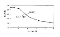
図4に、各データ電圧に対するキックバック電圧の変化率と共通電圧の変化率が示されている。図4の曲線は、データ電圧が6Vである時のキックバック電圧Vk(6)と、共通電圧Vcom(6)を基準に各データ電圧に対するキックバック電圧と共通電圧の相対的な変化率を示したもので、その関係式は下記式(3)、(4)に示すことができる。 FIG. 4 shows the rate of change of the kickback voltage and the rate of change of the common voltage for each data voltage. The curve in FIG. 4 shows the kickback voltage Vk (6) when the data voltage is 6V, and the relative change rates of the kickback voltage and the common voltage with respect to each data voltage based on the common voltage Vcom (6). The relational expression can be expressed by the following expressions (3) and (4).
キックバック電圧の変化率=[1+ΔVk6/Vk6]×100(%) …(3)
共通電圧の変化率=[1-ΔVcom6/Vcom6]×100(%) …(4)
ここで、ΔVk6=Vk-Vk6、ΔVcom6=Vcom-Vcom6である。
つまり、下記式(5)に示す関係式となる。
Change rate of kickback voltage = [1 + ΔVk6 / Vk6] × 100 (%) (3)
Change rate of common voltage = [1−ΔVcom6 / Vcom6] × 100 (%) (4)
Here, ΔVk6 = Vk−Vk6 and ΔVcom6 = Vcom−Vcom6.
That is, the relational expression shown in the following expression (5) is obtained.
ΔVk6/Vk6=-ΔVcom6/Vcom6 …(5)
図4では、データ電圧が増加するほどキックバック電圧の変化率及び共通電圧の変化率が減少することが示されている。この図4の関係を、前記式(3)に適用すると、データ電圧が増加するほどキックバック電圧の変化率が減少し、それによりキックバック電圧が減少することになる。共通電圧は、このようなキックバック電圧の変化を補償しなければならないので、データ電圧が増加するほど増加する必要がある。よって、階調電圧の平均階調値が大きくなるほど共通電圧を大きくする。
ΔVk6 / Vk6 = -ΔVcom6 / Vcom6 (5)
FIG. 4 shows that the rate of change of the kickback voltage and the rate of change of the common voltage decrease as the data voltage increases. When the relationship of FIG. 4 is applied to the above equation (3), the change rate of the kickback voltage decreases as the data voltage increases, and thus the kickback voltage decreases. The common voltage must compensate for such a change in kickback voltage, and thus needs to increase as the data voltage increases. Therefore, the larger the average grayscale value of the grayscale voltage, the higher the common voltage.
図4から、キックバック電圧の変化率と共通電圧の変化率がほぼ同一であるので、数式3により数式4が求められ、共通電圧がキックバック電圧の変化率を補償することができる。つまり、キックバック電圧の増加率と共通電圧の減少率がほぼ一致しており相互に補償し合っている。
From FIG. 4, since the rate of change of the kickback voltage and the rate of change of the common voltage are substantially the same, Equation 4 is obtained by
以上、本発明の好ましい実施例について詳細に説明したが、本発明の権利範囲はこれに限定されず、請求の範囲で定義している本発明の基本概念を利用した当業者の多様な変形及び改良形態も本発明の権利範囲に属するものである。 As described above, the preferred embodiments of the present invention have been described in detail, but the scope of the present invention is not limited thereto, and various modifications and alterations of those skilled in the art using the basic concept of the present invention defined in the appended claims can be made. Modifications also fall within the scope of the present invention.
100、200 表示板
190 画素電極
270 共通電極
300 液晶表示板組立体
400 ゲート駆動部
500 データ駆動部
600 信号制御部
710 可変共通電圧生成部
711 フレームメモリ
712 平均階調算出部
713 階調差算出部
714 デジタル-アナログ変換部
715〜718 反転増幅部
800 階調電圧生成部
100, 200
Claims (9)
複数の階調電圧を生成する階調電圧生成部と、
前記複数の階調電圧の中から映像データに該当する階調電圧を選択してデータ電圧として前記画素に印加するデータ駆動部と、
前記映像データを前記データ駆動部に提供し、前記映像データの制御のための制御信号を生成して前記データ駆動部に出力する信号制御部、そして
前記映像データの平均階調によって少なくとも一つの共通電圧を生成して前記画素に印加する共通電圧生成部を含む液晶表示装置。 A liquid crystal display device including a plurality of pixels arranged in a matrix,
A grayscale voltage generation unit that generates a plurality of grayscale voltages;
A data driver for selecting a gradation voltage corresponding to video data from the plurality of gradation voltages and applying the selected gradation voltage to the pixel as a data voltage;
A signal controller for providing the image data to the data driver, generating a control signal for controlling the image data, and outputting the control signal to the data driver; A liquid crystal display device including a common voltage generator for generating a voltage and applying the generated voltage to the pixel.
前記映像データを記憶するためのフレームメモリと、
前記映像データの平均階調を算出する平均階調算出部と、
前記平均階調算出部からの前記平均階調と基準階調との差を算出し、前記階調差に基づいて前記少なくとも一つの共通電圧に対する調整値を選択する階調差算出部と、
前記少なくとも一つの共通電圧を生成するための基準電圧を発生させる基準電圧生成部、そして
前記階調差算出部からの前記調整値に対応する基準電圧を前記調整値に基づいて変化させ、前記少なくとも一つの共通電圧を生成するD/A変換部をさらに含む請求項1に記載の液晶表示装置。 The common voltage generator includes:
A frame memory for storing the video data;
An average tone calculation unit that calculates an average tone of the video data,
Calculating a difference between the average grayscale and the reference grayscale from the average grayscale calculation unit, and selecting an adjustment value for the at least one common voltage based on the grayscale difference;
A reference voltage generation unit that generates a reference voltage for generating the at least one common voltage; and changing a reference voltage corresponding to the adjustment value from the gradation difference calculation unit based on the adjustment value; The liquid crystal display of claim 1, further comprising a D / A converter that generates one common voltage.
The liquid crystal display device according to claim 5, wherein the reference gray level is an intermediate gray level.
Applications Claiming Priority (2)
| Application Number | Priority Date | Filing Date | Title |
|---|---|---|---|
| KR1020020080817A KR100900548B1 (en) | 2002-12-17 | 2002-12-17 | Liquid crystal display for generating common voltages with different values |
| KR2002-080817 | 2002-12-17 |
Publications (2)
| Publication Number | Publication Date |
|---|---|
| JP2004199065A true JP2004199065A (en) | 2004-07-15 |
| JP4776877B2 JP4776877B2 (en) | 2011-09-21 |
Family
ID=32768476
Family Applications (1)
| Application Number | Title | Priority Date | Filing Date |
|---|---|---|---|
| JP2003417593A Expired - Fee Related JP4776877B2 (en) | 2002-12-17 | 2003-12-16 | Liquid crystal display device that generates common voltages of different magnitudes |
Country Status (4)
| Country | Link |
|---|---|
| US (1) | US7102604B2 (en) |
| JP (1) | JP4776877B2 (en) |
| KR (1) | KR100900548B1 (en) |
| TW (1) | TWI342415B (en) |
Cited By (6)
| Publication number | Priority date | Publication date | Assignee | Title |
|---|---|---|---|---|
| JP2006079044A (en) * | 2004-09-07 | 2006-03-23 | Samsung Electronics Co Ltd | Apparatus for generating analog driving voltage and common electrode voltage of liquid crystal display device and control method |
| JP2007178987A (en) * | 2005-12-28 | 2007-07-12 | Lg Philips Lcd Co Ltd | Apparatus and method for driving liquid crystal display element |
| JP2009282489A (en) * | 2008-05-19 | 2009-12-03 | Lg Display Co Ltd | Liquid crystal display for enhancing display quality, and driving method therefor |
| JP2013530424A (en) * | 2010-06-04 | 2013-07-25 | プラスティック ロジック リミテッド | Display device tuning |
| WO2015007000A1 (en) * | 2013-07-19 | 2015-01-22 | 深圳市华星光电技术有限公司 | Voltage compensation circuit and method for grid electrode driver and liquid-crystal display device |
| WO2017090727A1 (en) * | 2015-11-25 | 2017-06-01 | 国立大学法人 東京大学 | Electrostatic induction type power generation element |
Families Citing this family (57)
| Publication number | Priority date | Publication date | Assignee | Title |
|---|---|---|---|---|
| KR100527089B1 (en) * | 2002-11-04 | 2005-11-09 | 비오이 하이디스 테크놀로지 주식회사 | Common voltage regulating circuit of liquid crystal display device |
| KR100900548B1 (en) * | 2002-12-17 | 2009-06-02 | 삼성전자주식회사 | Liquid crystal display for generating common voltages with different values |
| KR100520383B1 (en) * | 2003-03-18 | 2005-10-11 | 비오이 하이디스 테크놀로지 주식회사 | Reference voltage generating circuit of liquid crystal display device |
| KR100514182B1 (en) * | 2003-09-08 | 2005-09-13 | 삼성에스디아이 주식회사 | Electro Luminescence display panel |
| GB0402046D0 (en) * | 2004-01-29 | 2004-03-03 | Koninkl Philips Electronics Nv | Active matrix display device |
| JP4356617B2 (en) * | 2005-01-20 | 2009-11-04 | セイコーエプソン株式会社 | Power supply circuit, display driver, electro-optical device, electronic apparatus, and control method for power supply circuit |
| JP4356616B2 (en) * | 2005-01-20 | 2009-11-04 | セイコーエプソン株式会社 | Power supply circuit, display driver, electro-optical device, electronic apparatus, and control method for power supply circuit |
| TWI302687B (en) * | 2005-02-02 | 2008-11-01 | Gigno Technology Co Ltd | Lcd panel and lcd device |
| KR101182557B1 (en) * | 2005-06-24 | 2012-10-02 | 엘지디스플레이 주식회사 | Liquid crystal display device and method for manufacturing thereof |
| TWI260568B (en) * | 2005-07-15 | 2006-08-21 | Au Optronics Corp | Driving system and method for liquid crystal display |
| KR20070056779A (en) * | 2005-11-30 | 2007-06-04 | 삼성전자주식회사 | Data drive integrated circuit device and liquid crystal display device comprising the same |
| US20070152955A1 (en) * | 2005-12-29 | 2007-07-05 | Nokia Corporation | Reduced power consumption display panel |
| KR101219043B1 (en) * | 2006-01-26 | 2013-01-07 | 삼성디스플레이 주식회사 | Display device and driving apparatus thereof |
| TW200734724A (en) * | 2006-03-03 | 2007-09-16 | Gigno Technology Co Ltd | LCD panel and LCD device |
| KR20070117295A (en) * | 2006-06-08 | 2007-12-12 | 삼성전자주식회사 | Liquid crystal display device and driving integrated circuit chip thereof |
| KR101222978B1 (en) * | 2006-06-29 | 2013-01-17 | 엘지디스플레이 주식회사 | Apparatus and method for driving of liquid crystal display device |
| KR101279117B1 (en) * | 2006-06-30 | 2013-06-26 | 엘지디스플레이 주식회사 | OLED display and drive method thereof |
| KR101337261B1 (en) * | 2006-07-24 | 2013-12-05 | 삼성디스플레이 주식회사 | Liquid crystal display and driving method thereof |
| KR101320019B1 (en) * | 2006-08-03 | 2013-10-18 | 삼성디스플레이 주식회사 | Driving IC, liquid crystal display and display system |
| US20080062111A1 (en) * | 2006-09-13 | 2008-03-13 | Himax Technologies Limited | Apparatus for Driving a Display |
| US7773104B2 (en) * | 2006-09-13 | 2010-08-10 | Himax Technologies Limited | Apparatus for driving a display and gamma voltage generation circuit thereof |
| TW200828244A (en) * | 2006-12-25 | 2008-07-01 | Himax Tech Ltd | Common voltage adjustment apparatus |
| KR101361621B1 (en) | 2007-02-15 | 2014-02-11 | 삼성디스플레이 주식회사 | Display device and method for driving the same |
| KR20080077495A (en) * | 2007-02-20 | 2008-08-25 | 삼성전자주식회사 | Circuit board and liquid crystal display comprising the same |
| CN101303490B (en) * | 2007-05-09 | 2010-05-26 | 群康科技(深圳)有限公司 | LCD device and public voltage adjustment method |
| CN101311781B (en) * | 2007-05-25 | 2012-02-08 | 群康科技(深圳)有限公司 | LCD device and its public voltage drive method |
| CN101312014B (en) * | 2007-05-25 | 2010-08-25 | 群康科技(深圳)有限公司 | Liquid crystal display device and driving method thereof |
| CN101344657B (en) * | 2007-07-13 | 2010-07-14 | 群康科技(深圳)有限公司 | LCD and common voltage driving method |
| KR101469040B1 (en) | 2008-01-02 | 2014-12-05 | 삼성디스플레이 주식회사 | Liquid crystal display device and driving methode thereof |
| CN101546528B (en) * | 2008-03-28 | 2011-05-18 | 群康科技(深圳)有限公司 | Liquid crystal display device and drive method thereof |
| JP2009294499A (en) * | 2008-06-06 | 2009-12-17 | Oki Semiconductor Co Ltd | Liquid crystal display device and liquid crystal display controller |
| KR101492564B1 (en) * | 2008-08-06 | 2015-03-06 | 삼성디스플레이 주식회사 | Liquid crystal display apparatus and common voltage control method thereof |
| CN101847376B (en) * | 2009-03-25 | 2013-10-30 | 北京京东方光电科技有限公司 | Common electrode driving circuit and LCD |
| US8373729B2 (en) * | 2010-03-22 | 2013-02-12 | Apple Inc. | Kickback compensation techniques |
| CN102446475B (en) | 2010-10-14 | 2016-08-31 | 上海天马微电子有限公司 | The pixel electrode voltage testing circuit of panel display apparatus |
| KR20120121715A (en) * | 2011-04-27 | 2012-11-06 | 삼성디스플레이 주식회사 | Display apparatus |
| CN102183852B (en) * | 2011-05-09 | 2013-07-17 | 深圳市华星光电技术有限公司 | Liquid crystal display |
| CN102629454B (en) * | 2011-06-16 | 2014-04-02 | 北京京东方光电科技有限公司 | Driver circuit of liquid crystal panel and method and system for driving liquid crystal display panel |
| CN102881263A (en) * | 2011-07-13 | 2013-01-16 | 冠捷投资有限公司 | Liquid crystal display equipment, panel driving device and common calibrating and adjusting module |
| US9019188B2 (en) | 2011-08-08 | 2015-04-28 | Samsung Display Co., Ltd. | Display device for varying different scan ratios for displaying moving and still images and a driving method thereof |
| US9165518B2 (en) | 2011-08-08 | 2015-10-20 | Samsung Display Co., Ltd. | Display device and driving method thereof |
| JP5731350B2 (en) * | 2011-10-11 | 2015-06-10 | 株式会社ジャパンディスプレイ | Liquid crystal display |
| US9299301B2 (en) | 2011-11-04 | 2016-03-29 | Samsung Display Co., Ltd. | Display device and method for driving the display device |
| US9208736B2 (en) | 2011-11-28 | 2015-12-08 | Samsung Display Co., Ltd. | Display device and driving method thereof |
| CN103185974B (en) * | 2011-12-28 | 2015-06-17 | 上海天马微电子有限公司 | Liquid crystal display device, liquid crystal display panel and method for adjusting common voltage of liquid crystal display panel |
| US9129572B2 (en) | 2012-02-21 | 2015-09-08 | Samsung Display Co., Ltd. | Display device and related method |
| US20130321378A1 (en) * | 2012-06-01 | 2013-12-05 | Apple Inc. | Pixel leakage compensation |
| TWI451397B (en) * | 2012-07-13 | 2014-09-01 | Richtek Technology Corp | Programmable gamma circuit for lcd display device and related method and driver circuit |
| TWI494908B (en) * | 2012-11-14 | 2015-08-01 | Novatek Microelectronics Corp | Liquid crystal display monitor and source driver and control method thereof |
| CN104281352B (en) * | 2014-10-13 | 2017-06-06 | 京东方科技集团股份有限公司 | A kind of In-cell touch panel and display device |
| KR102468762B1 (en) * | 2015-12-14 | 2022-11-21 | 엘지디스플레이 주식회사 | Display device with a built-in touch screen and method for driving the same |
| CN105741813B (en) * | 2016-05-11 | 2018-01-12 | 京东方科技集团股份有限公司 | System, method and display device for image procossing |
| US10580381B2 (en) * | 2017-05-17 | 2020-03-03 | Apple Inc. | Digital VCOM compensation for reducing display artifacts |
| CN107393493B (en) * | 2017-08-09 | 2020-11-13 | 京东方科技集团股份有限公司 | COM electrode, COM electrode driving method and display device |
| JP2019174774A (en) * | 2018-03-29 | 2019-10-10 | パナソニック液晶ディスプレイ株式会社 | Liquid crystal display device |
| CN108986756B (en) * | 2018-07-17 | 2020-04-28 | 深圳市华星光电半导体显示技术有限公司 | Common voltage feedback compensation circuit and method and liquid crystal display device |
| CN117079617B (en) * | 2023-10-12 | 2024-02-13 | 惠科股份有限公司 | Brightness adjusting method for display panel and display panel |
Citations (3)
| Publication number | Priority date | Publication date | Assignee | Title |
|---|---|---|---|---|
| JPH05341732A (en) * | 1992-06-05 | 1993-12-24 | Fujitsu Ltd | Active matrix type liquid crystal display device |
| JPH0933892A (en) * | 1995-07-20 | 1997-02-07 | Hitachi Ltd | Liquid crystal display device |
| JP2000322031A (en) * | 1999-05-10 | 2000-11-24 | Hitachi Ltd | Liquid crystal display device |
Family Cites Families (6)
| Publication number | Priority date | Publication date | Assignee | Title |
|---|---|---|---|---|
| JPH09152847A (en) * | 1995-09-29 | 1997-06-10 | Sharp Corp | Driving method for liquid crystal display panel and driving circuit therefor |
| TW375696B (en) * | 1996-06-06 | 1999-12-01 | Toshiba Corp | Display device |
| TW523622B (en) * | 1998-12-24 | 2003-03-11 | Samsung Electronics Co Ltd | Liquid crystal display |
| KR100593314B1 (en) * | 2000-07-24 | 2006-06-26 | 엘지.필립스 엘시디 주식회사 | liquid crystal display device |
| KR100840331B1 (en) * | 2002-08-07 | 2008-06-20 | 삼성전자주식회사 | common voltage generating device and liquid crystal device using the same |
| KR100900548B1 (en) * | 2002-12-17 | 2009-06-02 | 삼성전자주식회사 | Liquid crystal display for generating common voltages with different values |
-
2002
- 2002-12-17 KR KR1020020080817A patent/KR100900548B1/en active IP Right Grant
-
2003
- 2003-08-08 US US10/637,480 patent/US7102604B2/en active Active
- 2003-08-12 TW TW092122117A patent/TWI342415B/en not_active IP Right Cessation
- 2003-12-16 JP JP2003417593A patent/JP4776877B2/en not_active Expired - Fee Related
Patent Citations (3)
| Publication number | Priority date | Publication date | Assignee | Title |
|---|---|---|---|---|
| JPH05341732A (en) * | 1992-06-05 | 1993-12-24 | Fujitsu Ltd | Active matrix type liquid crystal display device |
| JPH0933892A (en) * | 1995-07-20 | 1997-02-07 | Hitachi Ltd | Liquid crystal display device |
| JP2000322031A (en) * | 1999-05-10 | 2000-11-24 | Hitachi Ltd | Liquid crystal display device |
Cited By (9)
| Publication number | Priority date | Publication date | Assignee | Title |
|---|---|---|---|---|
| JP2006079044A (en) * | 2004-09-07 | 2006-03-23 | Samsung Electronics Co Ltd | Apparatus for generating analog driving voltage and common electrode voltage of liquid crystal display device and control method |
| JP4730685B2 (en) * | 2004-09-07 | 2011-07-20 | サムスン エレクトロニクス カンパニー リミテッド | Analog drive voltage and common electrode voltage generator and control method for liquid crystal display |
| JP2007178987A (en) * | 2005-12-28 | 2007-07-12 | Lg Philips Lcd Co Ltd | Apparatus and method for driving liquid crystal display element |
| JP2009282489A (en) * | 2008-05-19 | 2009-12-03 | Lg Display Co Ltd | Liquid crystal display for enhancing display quality, and driving method therefor |
| JP2013530424A (en) * | 2010-06-04 | 2013-07-25 | プラスティック ロジック リミテッド | Display device tuning |
| WO2015007000A1 (en) * | 2013-07-19 | 2015-01-22 | 深圳市华星光电技术有限公司 | Voltage compensation circuit and method for grid electrode driver and liquid-crystal display device |
| WO2017090727A1 (en) * | 2015-11-25 | 2017-06-01 | 国立大学法人 東京大学 | Electrostatic induction type power generation element |
| JPWO2017090727A1 (en) * | 2015-11-25 | 2018-09-13 | 国立大学法人 東京大学 | Static induction generator |
| US10855204B2 (en) | 2015-11-25 | 2020-12-01 | The University Of Tokyo | Electrostatic induction type power generation element |
Also Published As
| Publication number | Publication date |
|---|---|
| US7102604B2 (en) | 2006-09-05 |
| KR20040053641A (en) | 2004-06-24 |
| JP4776877B2 (en) | 2011-09-21 |
| US20040169627A1 (en) | 2004-09-02 |
| TW200413782A (en) | 2004-08-01 |
| KR100900548B1 (en) | 2009-06-02 |
| TWI342415B (en) | 2011-05-21 |
Similar Documents
| Publication | Publication Date | Title |
|---|---|---|
| JP4776877B2 (en) | Liquid crystal display device that generates common voltages of different magnitudes | |
| KR101469040B1 (en) | Liquid crystal display device and driving methode thereof | |
| JP4621649B2 (en) | Display device and driving method thereof | |
| JP4683837B2 (en) | Liquid crystal display device having a plurality of gradation voltages, driving device and method thereof | |
| JP5704781B2 (en) | Display device and driving method thereof | |
| US10706759B2 (en) | Current comparison circuit, display device and driving method thereof | |
| JP2006209127A (en) | Liquid crystal display, display and method of driving display | |
| JP2006039205A (en) | Gradation voltage generation circuit, driving circuit, and electro-optical apparatus | |
| KR20080042433A (en) | Display device and driving apparatus thereof | |
| JP2006171761A (en) | Display device and driving method thereof | |
| JP2007156474A (en) | Liquid crystal display and modifying method of image signal thereof | |
| KR20120109890A (en) | Driving apparatus and driving method of liquid crsytal display | |
| JP2004226981A (en) | Device and method for driving liquid crystal display device generating digital gradation data according to gradation distribution | |
| KR101446999B1 (en) | Driving Circuit And Liquid Crystal Display Device Including The Same | |
| KR100945584B1 (en) | Apparatus of driving liquid crystal display | |
| JP2006350358A (en) | Display device, driving device of display device, and integrated circuit | |
| KR100785171B1 (en) | Liquid crystal display including gamma voltage generation circuit and driving method thereof | |
| KR100956344B1 (en) | Liquid crystal display | |
| KR20060118775A (en) | Driving apparatus of liquid crystal display | |
| KR100915239B1 (en) | Apparatus of driving liquid crystal display | |
| KR20170105176A (en) | Liquid crystal display device and driving method thereof | |
| KR20050005259A (en) | Apparatus and method of driving liquid crystal display | |
| KR20050050896A (en) | Liquid crystal display | |
| KR20060014551A (en) | Display device and driving device thereof | |
| KR20060119249A (en) | Driving apparatus for display device |
Legal Events
| Date | Code | Title | Description |
|---|---|---|---|
| A621 | Written request for application examination |
Free format text: JAPANESE INTERMEDIATE CODE: A621 Effective date: 20061201 |
|
| A977 | Report on retrieval |
Free format text: JAPANESE INTERMEDIATE CODE: A971007 Effective date: 20091222 |
|
| A131 | Notification of reasons for refusal |
Free format text: JAPANESE INTERMEDIATE CODE: A131 Effective date: 20100112 |
|
| A521 | Request for written amendment filed |
Free format text: JAPANESE INTERMEDIATE CODE: A523 Effective date: 20100406 |
|
| A131 | Notification of reasons for refusal |
Free format text: JAPANESE INTERMEDIATE CODE: A131 Effective date: 20100810 |
|
| A521 | Request for written amendment filed |
Free format text: JAPANESE INTERMEDIATE CODE: A523 Effective date: 20100916 |
|
| A131 | Notification of reasons for refusal |
Free format text: JAPANESE INTERMEDIATE CODE: A131 Effective date: 20101207 |
|
| A521 | Request for written amendment filed |
Free format text: JAPANESE INTERMEDIATE CODE: A523 Effective date: 20110221 |
|
| RD02 | Notification of acceptance of power of attorney |
Free format text: JAPANESE INTERMEDIATE CODE: A7422 Effective date: 20110221 |
|
| TRDD | Decision of grant or rejection written | ||
| A01 | Written decision to grant a patent or to grant a registration (utility model) |
Free format text: JAPANESE INTERMEDIATE CODE: A01 Effective date: 20110614 |
|
| A01 | Written decision to grant a patent or to grant a registration (utility model) |
Free format text: JAPANESE INTERMEDIATE CODE: A01 |
|
| A61 | First payment of annual fees (during grant procedure) |
Free format text: JAPANESE INTERMEDIATE CODE: A61 Effective date: 20110629 |
|
| R150 | Certificate of patent or registration of utility model |
Ref document number: 4776877 Country of ref document: JP Free format text: JAPANESE INTERMEDIATE CODE: R150 Free format text: JAPANESE INTERMEDIATE CODE: R150 |
|
| FPAY | Renewal fee payment (event date is renewal date of database) |
Free format text: PAYMENT UNTIL: 20140708 Year of fee payment: 3 |
|
| FPAY | Renewal fee payment (event date is renewal date of database) |
Free format text: PAYMENT UNTIL: 20140708 Year of fee payment: 3 |
|
| S111 | Request for change of ownership or part of ownership |
Free format text: JAPANESE INTERMEDIATE CODE: R313111 |
|
| FPAY | Renewal fee payment (event date is renewal date of database) |
Free format text: PAYMENT UNTIL: 20140708 Year of fee payment: 3 |
|
| R371 | Transfer withdrawn |
Free format text: JAPANESE INTERMEDIATE CODE: R371 |
|
| S111 | Request for change of ownership or part of ownership |
Free format text: JAPANESE INTERMEDIATE CODE: R313111 |
|
| R350 | Written notification of registration of transfer |
Free format text: JAPANESE INTERMEDIATE CODE: R350 |
|
| R250 | Receipt of annual fees |
Free format text: JAPANESE INTERMEDIATE CODE: R250 |
|
| R250 | Receipt of annual fees |
Free format text: JAPANESE INTERMEDIATE CODE: R250 |
|
| R250 | Receipt of annual fees |
Free format text: JAPANESE INTERMEDIATE CODE: R250 |
|
| R250 | Receipt of annual fees |
Free format text: JAPANESE INTERMEDIATE CODE: R250 |
|
| R250 | Receipt of annual fees |
Free format text: JAPANESE INTERMEDIATE CODE: R250 |
|
| R250 | Receipt of annual fees |
Free format text: JAPANESE INTERMEDIATE CODE: R250 |
|
| R250 | Receipt of annual fees |
Free format text: JAPANESE INTERMEDIATE CODE: R250 |
|
| LAPS | Cancellation because of no payment of annual fees |