JP2004187366A - General-purpose charging arrangement - Google Patents
General-purpose charging arrangement Download PDFInfo
- Publication number
- JP2004187366A JP2004187366A JP2002349243A JP2002349243A JP2004187366A JP 2004187366 A JP2004187366 A JP 2004187366A JP 2002349243 A JP2002349243 A JP 2002349243A JP 2002349243 A JP2002349243 A JP 2002349243A JP 2004187366 A JP2004187366 A JP 2004187366A
- Authority
- JP
- Japan
- Prior art keywords
- circuit
- output voltage
- voltage
- battery
- output
- Prior art date
- Legal status (The legal status is an assumption and is not a legal conclusion. Google has not performed a legal analysis and makes no representation as to the accuracy of the status listed.)
- Granted
Links
Images

Classifications
-
- H—ELECTRICITY
- H02—GENERATION; CONVERSION OR DISTRIBUTION OF ELECTRIC POWER
- H02J—CIRCUIT ARRANGEMENTS OR SYSTEMS FOR SUPPLYING OR DISTRIBUTING ELECTRIC POWER; SYSTEMS FOR STORING ELECTRIC ENERGY
- H02J9/00—Circuit arrangements for emergency or stand-by power supply, e.g. for emergency lighting
- H02J9/005—Circuit arrangements for emergency or stand-by power supply, e.g. for emergency lighting using a power saving mode
-
- H—ELECTRICITY
- H02—GENERATION; CONVERSION OR DISTRIBUTION OF ELECTRIC POWER
- H02J—CIRCUIT ARRANGEMENTS OR SYSTEMS FOR SUPPLYING OR DISTRIBUTING ELECTRIC POWER; SYSTEMS FOR STORING ELECTRIC ENERGY
- H02J2207/00—Indexing scheme relating to details of circuit arrangements for charging or depolarising batteries or for supplying loads from batteries
- H02J2207/20—Charging or discharging characterised by the power electronics converter
-
- Y—GENERAL TAGGING OF NEW TECHNOLOGICAL DEVELOPMENTS; GENERAL TAGGING OF CROSS-SECTIONAL TECHNOLOGIES SPANNING OVER SEVERAL SECTIONS OF THE IPC; TECHNICAL SUBJECTS COVERED BY FORMER USPC CROSS-REFERENCE ART COLLECTIONS [XRACs] AND DIGESTS
- Y02—TECHNOLOGIES OR APPLICATIONS FOR MITIGATION OR ADAPTATION AGAINST CLIMATE CHANGE
- Y02B—CLIMATE CHANGE MITIGATION TECHNOLOGIES RELATED TO BUILDINGS, e.g. HOUSING, HOUSE APPLIANCES OR RELATED END-USER APPLICATIONS
- Y02B70/00—Technologies for an efficient end-user side electric power management and consumption
- Y02B70/30—Systems integrating technologies related to power network operation and communication or information technologies for improving the carbon footprint of the management of residential or tertiary loads, i.e. smart grids as climate change mitigation technology in the buildings sector, including also the last stages of power distribution and the control, monitoring or operating management systems at local level
-
- Y—GENERAL TAGGING OF NEW TECHNOLOGICAL DEVELOPMENTS; GENERAL TAGGING OF CROSS-SECTIONAL TECHNOLOGIES SPANNING OVER SEVERAL SECTIONS OF THE IPC; TECHNICAL SUBJECTS COVERED BY FORMER USPC CROSS-REFERENCE ART COLLECTIONS [XRACs] AND DIGESTS
- Y04—INFORMATION OR COMMUNICATION TECHNOLOGIES HAVING AN IMPACT ON OTHER TECHNOLOGY AREAS
- Y04S—SYSTEMS INTEGRATING TECHNOLOGIES RELATED TO POWER NETWORK OPERATION, COMMUNICATION OR INFORMATION TECHNOLOGIES FOR IMPROVING THE ELECTRICAL POWER GENERATION, TRANSMISSION, DISTRIBUTION, MANAGEMENT OR USAGE, i.e. SMART GRIDS
- Y04S20/00—Management or operation of end-user stationary applications or the last stages of power distribution; Controlling, monitoring or operating thereof
- Y04S20/20—End-user application control systems
Abstract
Description
【0001】
【発明が属する技術分野】
本発明は、携帯用機器等の電源として用いられている異なる素電池数の電池組を一台の充電装置で充電することができる汎用充電装置に関する。
【0002】
【従来の技術】
充電装置として種々のものがあり、特に異なる素電池数の電池組すなわち電池電圧の異なる電池組を一台の充電装置で充電することができる汎用充電装置が普及している。例えば、1.2Vの素電池をそれぞれ9個、10個、12個直列に接続してなる9.6V、12V、14.4Vの電池電圧を有する3種類の電池組は汎用充電装置があれば1台で充電することができる。
【0003】
【発明が解決しようとする課題】
しかしながら、異なる素電池の電池組を全て充電する汎用充電装置においては、汎用充電装置が充電可能な最も素電池数の多い電池組に対応した出力電圧となるような制御が行われているため、素電池数の少ない電池組を実装して充電しようとした場合、この電池組を充電すべくスイッチ回路を閉じると、定電圧制御されている素電池数の多い電池組に対応した出力電圧が、素電池数の少ない電池組に印加され、スイッチ回路が閉じた瞬間過渡的に電池組に大きな突入電流が流れる。この結果、この充電ループに存在するスイッチ回路に大きなダメージを与えてしまうという問題がある。
【0004】
また、電池組が実装されていない時や、電池組が満充電と判別され充電を終了するときにはスイッチ回路をオフし、充電電流の供給を遮断するが、電源回路は、充電可能な最も素電池数の多い電池組に対応した出力電圧となるよう制御されているため、消費電力が大きくなるという問題もある。
【0005】
本発明の目的は上記した従来技術の欠点をなくし,充電待機時の低電力化と、充電開始時の電池組に流れる突入電流を抑制する汎用充電装置を提供するものである。
【0006】
【課題を解決するための手段】
上記目的を達成するため、請求項1に記載の汎用充電装置は、電池電圧の異なる電池組を一台の充電装置で充電するものであって、電池組へ充電電流を供給する電源回路と、電池組への充電電流の供給をオン・オフするスイッチと、該電源回路の出力電圧を検出する出力電圧検出回路と、電池組の電池電圧を検出する電池電圧検出回路とを備え、該スイッチをオンする前に該電源回路の出力電圧を変化させて、該電源回路の該出力電圧と該電池電圧検出回路が検出した電池組の電池電圧との差が所定範囲内になったときに該スイッチをオンする制御手段を備えたことを特徴としている。
【0007】
請求項2に記載の汎用充電装置は、電池電圧の異なる電池組を一台の充電装置で充電するものであって、電池組へ充電電流を供給する電源回路と、該電源回路の出力電圧を検出する出力電圧検出回路と、出力電圧を複数の出力電圧に設定することが可能な出力電圧設定回路と、前記出力電圧検出回路と出力電圧設定回路の出力に基づいて前記電源回路に帰還をかけ出力電圧を所定の電圧に制御する出力電圧制御回路と、充電電流を検出する充電電流検出回路と、充電電流を設定する充電電流設定回路と、前記充電電流検出回路と充電電流設定回路との出力に基づいて前記電源回路に帰還をかけ充電電流を制御する充電電流制御回路と、電池組への充電電流の供給をオン・オフするスイッチと、該スイッチ回路を駆動するスイッチ駆動回路と、電池組の電池電圧を検出する電池電圧検出回路と、該電池電圧検出回路の出力に基づいて前記出力電圧設定回路、前記充電電流設定回路、及び前記スイッチ駆動回路を制御するマイコンと、該マイコンの電源となる前記電源回路からの出力を定電圧化する定電圧回路を備え、前記マイコンは、前記スイッチ駆動回路を介して前記スイッチをオンさせ、前記電源回路から電池組に充電電流を供給するときは、前記出力電圧設定回路を充電中の電池電圧より大きくなる第一の出力電圧で設定し、充電中は前記充電電流制御御回路の出力に基づいて所定の充電電流になるよう制御し、前記スイッチ駆動回路を介して前記スイッチをオフしている時は、前記出力電圧設定回路を第一の出力電圧より低い第二の出力電圧で設定し、前記出力電圧制御回路の出力に基づいて第二の出力電圧になるよう制御することを特徴としている。
【0008】
請求項3に記載の汎用充電装置は、請求項2記載の装置において、前記マイコンが前記スイッチ駆動回路を介して前記スイッチがオフ状態からオン状態にさせる時は、前記スイッチ回路の開閉速度に併せて、前記出力電圧設定回路を介して出力電圧を第二の出力電圧から第一の出力電圧に切り替える信号を出力するように制御することを特徴としている。
【0009】
請求項4記載の汎用充電装置は、請求項2記載の汎用充電装置において、前記マイコンは充電中の電池組の電池電圧に対応しその電池電圧より大きい第一の出力電圧を設定し、前記出力電圧設定回路に出力するようにしたことを特徴としている。
【0010】
請求項5に記載の汎用充電装置は、請求項2記載の装置に対して、前記マイコンは前記スイッチ駆動回路を介して前記スイッチがオン状態からオフ状態にさせる時に対応して、前記出力電圧設定回路を介して出力電圧を第一の出力電圧から第二の出力電圧に切り替えるとともに、前記マイコンの電源をとなる前記定電圧回路は、前記電源回路の出力が第一の出力電圧から第二の出力電圧に減衰する時間は前記マイコンが動作する所定の電圧を維持できる能力を有することを特徴としている。
【0011】
かかる構成の汎用充電装置では、電池組に充電電流を供給するときは、充電中の電池電圧より大きくなる第一の出力電圧で設定し、充電中は所定の充電電流になるよう制御し、充電待機中は第一の出力電圧より低い第二の出力電圧で設定し、第二の出力電圧になるよう制御している。
【0012】
【発明の実施の形態】
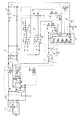
図1は本発明の実施の形態に係わる汎用充電装置の構成を示した回路図である。図において,1は交流電源、2は複数の素電池を直列接続した電池組、3は電池組2に流れる充電電流を検出する電流検出回路、4は抵抗4a、4bからなる出力電圧検出回路で、電源回路の2次側整流平滑回路30の出力電圧を抵抗4a、4bで分圧し、出力電圧制御回路80に入力する。5は2次側整流平滑回路30の出力電圧、及び充電電流の信号をSW制御IC23に帰還する信号伝達手段であり、ホトカプラ等からなる。6は電池組2への充電電流の供給をオン・オフせしめるスイッチ回路で、リレーから構成されており、電池組2に充電電流を供給する時は、リレーをオンし、それ以外の電池組2が実装されていないときや、電池組2が満充電と判別され、充電を終了させるときはリレーをオフさせ充電電流の供給を遮断する。
【0013】
7はスイッチ回路をドライブするスイッチ駆動回路であり、マイコン50の出力ポート56の出力に基づいてスイッチ6をドライブする例えばデジタルトランジスタから構成されている。
【0014】
8は抵抗8a、8b、8c、8dからなる出力電圧設定回路で、抵抗8a、8bの分圧比で設定された電圧値を、抵抗8c、抵抗8dに連なる夫々の出力ポートを“L”レベルに選択することで電圧値を変えられ、抵抗8c、抵抗8dに連なる夫々の出力ポートを“ハイ・インピーダンス”レベルにすることも可能であり、これにより4種の2次側整流平滑回路30の出力電圧に相当する電圧値を選択でき、出力電圧を制御するための基準電圧になる。
【0015】
9は抵抗9a、9b、9c、9dからなる充電電流設定回路であり、出力ポート56からの信号に対応して演算増幅器62の反転入力端に印加する電圧値を変えるものであり、抵抗9a、9bの分圧比で設定された電圧値を、抵抗9c、抵抗9dに連なる夫々の出力ポートを“L”レベルに選択することで電圧値を変えられ、抵抗9c、抵抗9dに連なる夫々の出力ポートを“ハイ・インピーダンス”レベルにすることも可能であり、これにより4種の電流値に相当する電圧値を選択できる。
【0016】
10は全波整流回路11と平滑用コンデンサ12からなる1次側整流平滑回路、20は高周波トランス21、MOSFET22とSW制御IC23、SW制御IC用定電圧回路24、起動抵抗25からなるスイッチング回路であり、高周波トランス21は1次巻線21a、2次巻線21b,3次巻線21c,4次巻線21dからなり,直流の入力電圧が印可される1次巻線21aに対し,2次巻線21bはSW制御IC用の出力巻線、3次巻線21cは電池組2を充電するための出力巻線,4次巻線21dはマイコン50,充電電流制御手段60等の電源用の出力巻線である。なお1次巻線21aに対し,2次巻線21b,4次巻線21dは同極性の構成であり,3次巻線21cは逆極性である。SW制御IC23はMOSFET22の駆動パルス幅を変えて出力電圧を調整するスイッチング電源ICである。また、SW制御IC用定電圧回路24はダイオード24a、3端子レギュレータ24b、コンデンサ24c、24dから構成されおり、2次巻線21bからの出力電圧を定電圧化する。
【0017】
30はダイオード31、平滑用コンデンサ32、抵抗33からなる2次側整流平滑回路、40は抵抗41、42からなる電池電圧検出回路で、電池組2の端子電圧を分圧する。50は演算手段(CPU)51、ROM52、RAM53、タイマ54、A/Dコンバータ55、出力ポート56、リセット入力ポート57からなるマイコンである。CPU51は、A/Dコンバータ55の入力データに基づいて、サンプリングごとに最新の電池電圧と複数サンプリング前の電池電圧とを比較し、その結果に基づいて電池組2の満充電は判別する。RAM53はサンプリングした最新の電池電圧までの所定数のサンプリングした電池電圧を記憶する。
【0018】
60は演算増幅器61、62、抵抗63〜67、ダイオード68からなる充電電流制御回路であり、充電電流検出回路3に流れる充電電流を検出し、この充電電流に対応する電圧を反転増幅させた出力電圧と、充電電流設定回路9で設定された充電電流設定基準電圧との差を増幅し、信号伝達手段5を介してSW制御IC23に帰還をかけ制御する。すなわち、充電電流が大きい場合はパルス幅を狭めたパルスを、逆の場合はパルス幅を広げたパルスを高周波トランス21に与え整流平滑回路30で直流に平滑し、充電電流を一定に保つ。すなわち電流検出回路3、充電電流制御回路60、信号伝達手段5、スイッチング回路20、整流平滑回路30を介して充電電流を設定電流値となるように制御する。
【0019】
70は電源トランス71、全波整流回路72、平滑コンデンサ73、3端子レギュレータ74、リセットIC75からなる定電圧回路で、マイコン50、充電電流制御手段60等の電源となる。リセットIC75はマイコン50を初期状態にするためにリセット入力ポート57にリセット信号を出力する。
【0020】
80は演算増幅器81、抵抗82〜85、ダイオード86からなる出力電圧設定回路であり、出力電圧検出回路4からの電圧と出力電圧設定回路8からの電圧との差を増幅し、信号伝達手段5を介してSW制御IC23に帰還をかけ出力電圧を制御する。
【0021】
次に、本発明の実施の形態に係わる汎用充電装置の出力電圧制御方法について、図2に示したフローチャートに従って説明する。図2(a)は出力電圧制御方法の第1実施例に係わるフローチャートであり、図2(b)は第2実施例に係わるフローチャートである。
【0022】
図2(a)に示した第1実施例において、まず、電池組2が実装されているかどうかの判断がされる(S1)。電池組2が実装されていない場合は、電池組2が実装されるまで待機する。出力電圧設定回路8が出力電圧制御回路80に出力する電圧は、抵抗8c、抵抗8dに連なる出力ポート56からの出力(以下、それぞれを「第1ポート出力」、「第2ポート出力」という。)のそれぞれを“L”レベルあるいは“H”レベルにすることで4通りに可変することができ、これにより2次側整流平滑回路30から4通りの出力電圧を選択的に出力させることができる。
【0023】
電池組2が実装されていない充電待機時は(S1:NO)、2次側整流平滑回路30からの出力電圧が最も低くなるよう、例えば、第1ポート出力と第2ポート出力を共に“L”レベルとする。これにより、待機時における消費電力の低減化を図ることができる。
【0024】
電池組2が汎用充電装置に実装されると(S1:YES)、マイコン50は電池電圧検出回路40の出力に基づいて電池電圧を検出し(S2)、検出した電池電圧に基づいて第1ポート出力と第2ポート出力を決定する(S3)。例えば、第1ポート出力と第2ポート出力をそれぞれ“L”レベル、“H”レベルとすることにより2次側整流平滑回路30からの出力電圧が2番目に低くなるようにし、第1ポート出力と第2ポート出力をそれぞれ“H”レベル、“L”レベルとすることにより2次側整流平滑回路30からの出力電圧が3番目に低くなる(2番目に高くなる)ようにする。また、第1ポート出力と第2ポート出力を共に“H”レベルとすることにより2次側整流平滑回路30からの出力電圧が最も高くなるようにする。そして、検出した電池電圧が所定電圧以下(例えば、12V以下)の場合には、2番目に低い電圧、例えば、13Vが2次側整流平滑回路30から出力されるように第1出力ポートと第2出力ポートを制御し、検出した電池電圧が所定電圧よりも高い場合には、2番目に高い電圧が2次側整流平滑回路30から出力されるように第1出力ポートと第2出力ポートを制御する。
【0025】
通常、第1ポート出力と第2ポート出力は共に“H”レベルに設定されており、2次側整流平滑回路30からは、最も高い電圧、例えば、40Vの出力がある。上記の例で、検出した電池電圧が12Vの場合には、第1ポート出力と第2ポート出力をそれぞれ“H”レベル、“L”レベルに切り換え、2次側整流平滑回路30からの出力を13Vに落とす。このとき、コンデンサ32に蓄えられていた電荷が抵抗33を介して所定の時定数で放電されるため、第1ポート出力と第2ポート出力を切り換えた後、所定時間が経過したかどうかの判断を行う(S4A)。所定時間が経過し(S4A:YES)、2次側整流平滑回路30からの出力が13Vに落ちたところで、マイコン50は出力ポート56を介して、スイッチ駆動回路7に信号を出力してスイッチ6をオフ状態からオン状態にする(S5)。
【0026】
その後、第1の出力ポートと第2の出力ポートを共に“H”レベルに切り換え(S6)、出力電圧設定回路8を介して2次側整流平滑回路30からの出力電圧を、例えば、13Vから充電可能な40Vに増加させる。スイッチ6のリレーは実際の信号に対し、接点が閉じるまでには若干の時間遅れがあり、この時間遅れを補正するように、スイッチ駆動回路7に出力する信号に対して、出力電圧設定回路8に出力する信号を上記の時間に合わせて遅らせるようにすれば、リレーが閉じた瞬間、過渡的に電池組2に大きな突入電流を抑制し、この結果、この充電ループに存在するスイッチ回路6のリレーへのダメージをなくすることが可能になる。
【0027】
また、電池組2の充電が完了した場合等の、前記スイッチがオン状態からオフ状態にさせる時は、マイコン50は前記出力電圧設定回路8を介して出力電圧を充電時の電池電圧より高い設定電圧から、充電待機時の低電圧出力に切り替えるが、このときは、出力電圧を充電時の電池電圧より高い設定電圧から充電待機時の低電圧出力に減衰する間は、定電圧制御回路は電源回路の出力を絞る信号、すなわち、電源回路の出力をオフする信号を出力する。そのためマイコン50の電源をとなる定電圧回路70は、電源回路の出力が電池電圧より高い設定電圧から充電待機時の低電圧出力に減衰する時間はマイコン50が動作する所定の電圧を維持できる能力を有することが必要であり、この減衰する時間に対応して、定電圧回路70のコンデンサ72、73の容量を選定する必要がある。
【0028】
図2(b)に示したフローチャートは、図2(a)に示したフローチャートのS4Aの処理がS4Bの処理に変更された点のみが異なっている。S3で第1ポート出力と第2ポート出力の信号レベルが適宜決定されると、2次側整流平滑回路30からの出力電圧Voutが電池電圧Vin近傍まで低下したかどうかの判断を行う(S4B)。例えば、2次側整流平滑回路30からの出力電圧Voutが電池電圧Vinよりも5V以上低くなるまで待機し(S4B:YES)、その上でリレーを閉じるようにしている。出力電圧Voutと電池電圧Vinの比較を行うためには、2次側整流平滑回路30からの出力電圧VoutはA/D変換した値でなければならないので、電池電圧Vinを抵抗41,42を介してA/Dコンバータ55に入力するのと同様の構成が2次側整流平滑回路30の出力電圧をA/D変換するために必要となる。
【0029】
【発明の効果】
以上のように、請求項1乃至5記載の発明によれば,充電待機時の低電力化と、充電開始時の電池組に流れる突入電流を抑制することができる。
【図面の簡単な説明】
【図1】本発明の実施の形態に係わる汎用充電装置の構成を示した回路図。
【図2】(a)は図1に示した汎用充電装置の動作を説明した第1実施例に係わるフローチャート、(b)は第2実施例に係わるフローチャート。
【符号の説明】
2は電池組、3は充電電流検出回路、4は出力電圧検出回路、6はスイッチであるリレー、7はスイッチ駆動回路、8は出力電圧設定回路、9は充電電流設定回路、10は10は1次側整流平滑回路、20はスイッチング回路、30は2次側整流平滑回路、40は電池電圧検出回路、50はマイコン、60は充電電流制御回路、70定電圧回路で、80は出力電圧制御回路である。[0001]
TECHNICAL FIELD OF THE INVENTION
The present invention relates to a general-purpose charger that can charge a battery set having a different number of cells used as a power source of a portable device or the like with a single charger.
[0002]
[Prior art]
There are various types of charging devices, and in particular, general-purpose charging devices that can charge a battery set having a different number of unit cells, that is, a battery set having a different battery voltage, with a single charging device have become widespread. For example, three types of battery groups having battery voltages of 9.6V, 12V, and 14.4V, which are formed by connecting nine, ten, and twelve 1.2V cells in series, respectively, if a general-purpose charging device is available It can be charged by one unit.
[0003]
[Problems to be solved by the invention]
However, in a general-purpose charging device that charges all battery groups of different unit cells, control is performed such that an output voltage corresponding to the battery group with the largest number of unit cells that can be charged by the general-purpose charging device is performed. If a battery pack with a small number of cells is mounted and charging is attempted, and the switch circuit is closed to charge this battery pack, the output voltage corresponding to the battery pack with a large number of cells that is being controlled at a constant voltage is A large rush current is applied to the battery group with a small number of cells and transiently flows through the battery group momentarily when the switch circuit is closed. As a result, there is a problem that the switch circuit existing in the charging loop is seriously damaged.
[0004]
When the battery pack is not mounted, or when the battery pack is determined to be fully charged and charging is completed, the switch circuit is turned off and the supply of the charging current is shut off. Since the output voltage is controlled so as to correspond to a large number of battery groups, there is also a problem that power consumption increases.
[0005]
SUMMARY OF THE INVENTION An object of the present invention is to provide a general-purpose charging apparatus that eliminates the above-mentioned disadvantages of the prior art, reduces power consumption during standby for charging, and suppresses inrush current flowing through a battery set at the start of charging.
[0006]
[Means for Solving the Problems]
In order to achieve the above object, a general-purpose charging device according to claim 1 charges a battery set having a different battery voltage by a single charging device, and supplies a charging current to the battery set. A switch for turning on / off the supply of the charging current to the battery pack, an output voltage detection circuit for detecting the output voltage of the power supply circuit, and a battery voltage detection circuit for detecting the battery voltage of the battery pack; The output voltage of the power supply circuit is changed before turning on, and the switch is turned on when the difference between the output voltage of the power supply circuit and the battery voltage of the battery set detected by the battery voltage detection circuit is within a predetermined range. Is provided with control means for turning on.
[0007]
The general-purpose charging device according to
[0008]
The general-purpose charging device according to
[0009]
5. The general-purpose charging device according to claim 4, wherein the microcomputer sets a first output voltage corresponding to the battery voltage of the battery set being charged and higher than the battery voltage. It is characterized in that it is output to a voltage setting circuit.
[0010]
A general-purpose charging device according to
[0011]
In the general-purpose charging device having such a configuration, when a charging current is supplied to the battery set, the charging current is set at a first output voltage that is higher than the battery voltage during charging, and is controlled to a predetermined charging current during charging. During standby, the second output voltage is set lower than the first output voltage, and the output voltage is controlled to the second output voltage.
[0012]
BEST MODE FOR CARRYING OUT THE INVENTION
FIG. 1 is a circuit diagram showing a configuration of a general-purpose charging device according to an embodiment of the present invention. In the drawing, 1 is an AC power supply, 2 is a battery set in which a plurality of unit cells are connected in series, 3 is a current detection circuit for detecting a charging current flowing through the
[0013]
Reference numeral 7 denotes a switch drive circuit for driving the switch circuit, which is composed of, for example, a digital transistor for driving the
[0014]
[0015]
[0016]
[0017]
[0018]
[0019]
[0020]
[0021]
Next, an output voltage control method of the general-purpose charging device according to the embodiment of the present invention will be described with reference to the flowchart shown in FIG. FIG. 2A is a flowchart according to the first embodiment of the output voltage control method, and FIG. 2B is a flowchart according to the second embodiment.
[0022]
In the first embodiment shown in FIG. 2A, first, it is determined whether or not the battery set 2 is mounted (S1). If the battery set 2 is not mounted, the process waits until the battery set 2 is mounted. The voltage output from the output
[0023]
When the
[0024]
When the battery set 2 is mounted on the general-purpose charging device (S1: YES), the microcomputer 50 detects the battery voltage based on the output of the battery voltage detection circuit 40 (S2), and determines the first port based on the detected battery voltage. An output and a second port output are determined (S3). For example, the first port output and the second port output are set to “L” level and “H” level, respectively, so that the output voltage from the secondary side rectifying / smoothing
[0025]
Normally, both the first port output and the second port output are set to “H” level, and the secondary side rectifying / smoothing
[0026]
Thereafter, both the first output port and the second output port are switched to the “H” level (S6), and the output voltage from the secondary side rectifying / smoothing
[0027]
When the switch is turned off from the on state, for example, when the charging of the battery set 2 is completed, the microcomputer 50 sets the output voltage higher than the battery voltage at the time of charging via the output
[0028]
The flowchart shown in FIG. 2B is different only in that the process of S4A in the flowchart shown in FIG. 2A is changed to the process of S4B. When the signal levels of the first port output and the second port output are appropriately determined in S3, it is determined whether or not the output voltage Vout from the secondary rectifying / smoothing
[0029]
【The invention's effect】
As described above, according to the first to fifth aspects of the present invention, it is possible to reduce the power consumption at the time of charging standby and to suppress the rush current flowing through the battery assembly at the start of charging.
[Brief description of the drawings]
FIG. 1 is a circuit diagram showing a configuration of a general-purpose charging device according to an embodiment of the present invention.
2A is a flowchart according to a first embodiment illustrating the operation of the general-purpose charging device shown in FIG. 1, and FIG. 2B is a flowchart according to a second embodiment.
[Explanation of symbols]
2 is a battery set, 3 is a charging current detection circuit, 4 is an output voltage detection circuit, 6 is a relay which is a switch, 7 is a switch drive circuit, 8 is an output voltage setting circuit, 9 is a charging current setting circuit, 10 is 10 Primary side rectifying and smoothing circuit, 20 is a switching circuit, 30 is a secondary side rectifying and smoothing circuit, 40 is a battery voltage detecting circuit, 50 is a microcomputer, 60 is a charging current control circuit, 60 is a constant voltage circuit, and 80 is output voltage control. Circuit.
Claims (5)
Priority Applications (5)
| Application Number | Priority Date | Filing Date | Title |
|---|---|---|---|
| JP2002349243A JP4536997B2 (en) | 2002-11-29 | 2002-11-29 | Charger |
| CNB2003101195155A CN100413175C (en) | 2002-11-29 | 2003-12-01 | Universal battery charger |
| US10/724,205 US7365515B2 (en) | 2002-11-29 | 2003-12-01 | Universal battery charger |
| EP03257561A EP1424758B1 (en) | 2002-11-29 | 2003-12-01 | Universal battery charger |
| DE60327978T DE60327978D1 (en) | 2002-11-29 | 2003-12-01 | Universal battery charger |
Applications Claiming Priority (1)
| Application Number | Priority Date | Filing Date | Title |
|---|---|---|---|
| JP2002349243A JP4536997B2 (en) | 2002-11-29 | 2002-11-29 | Charger |
Publications (3)
| Publication Number | Publication Date |
|---|---|
| JP2004187366A true JP2004187366A (en) | 2004-07-02 |
| JP2004187366A5 JP2004187366A5 (en) | 2005-12-22 |
| JP4536997B2 JP4536997B2 (en) | 2010-09-01 |
Family
ID=32290512
Family Applications (1)
| Application Number | Title | Priority Date | Filing Date |
|---|---|---|---|
| JP2002349243A Expired - Fee Related JP4536997B2 (en) | 2002-11-29 | 2002-11-29 | Charger |
Country Status (5)
| Country | Link |
|---|---|
| US (1) | US7365515B2 (en) |
| EP (1) | EP1424758B1 (en) |
| JP (1) | JP4536997B2 (en) |
| CN (1) | CN100413175C (en) |
| DE (1) | DE60327978D1 (en) |
Cited By (10)
| Publication number | Priority date | Publication date | Assignee | Title |
|---|---|---|---|---|
| EP1701426A2 (en) | 2005-03-11 | 2006-09-13 | Hitachi Koki Co., Ltd. | Battery charger |
| EP1950862A2 (en) | 2007-01-29 | 2008-07-30 | Hitachi Koki Co., Ltd. | Charging device |
| JP2009177963A (en) * | 2008-01-25 | 2009-08-06 | Hitachi Koki Co Ltd | Charging device |
| JP2010016984A (en) * | 2008-07-03 | 2010-01-21 | Sanyo Electric Co Ltd | Charging controller and charging equipment |
| US7652450B2 (en) | 2005-09-13 | 2010-01-26 | Hitachi Koki Co., Ltd. | Secondary battery charging device |
| JP2010045922A (en) * | 2008-08-12 | 2010-02-25 | Hitachi Koki Co Ltd | Charger |
| JP2013070453A (en) * | 2011-09-20 | 2013-04-18 | Panasonic Eco Solutions Power Tools Co Ltd | Charger |
| US8841880B2 (en) | 2009-10-29 | 2014-09-23 | Hitachi Koki Co., Ltd. | Battery charger with charge abnormality checking function |
| WO2014156514A1 (en) | 2013-03-28 | 2014-10-02 | Hitachi Koki Co., Ltd. | Charging device |
| JP2022044030A (en) * | 2020-09-04 | 2022-03-16 | 三星エスディアイ株式会社 | Charging system and charger for reducing inrush current |
Families Citing this family (14)
| Publication number | Priority date | Publication date | Assignee | Title |
|---|---|---|---|---|
| JP4148183B2 (en) * | 2004-05-18 | 2008-09-10 | 日立工機株式会社 | Charger |
| US7696717B2 (en) * | 2005-08-08 | 2010-04-13 | Continental Automotive Systems Us, Inc. | Battery energy management system for measuring a minimum battery voltage |
| KR100954035B1 (en) | 2006-05-08 | 2010-04-20 | 삼성에스디아이 주식회사 | Method of charging rechargeable battery and Protection circuit for rechargeable battery |
| JP4413236B2 (en) * | 2007-02-16 | 2010-02-10 | セイコーエプソン株式会社 | Power reception control device, power transmission control device, non-contact power transmission system, power reception device, power transmission device, and electronic device |
| US8358103B2 (en) * | 2008-07-04 | 2013-01-22 | Vampire Labs, Llc | Automatic coupling of an alternating current power source and an inductive power apparatus to charge a target device battery |
| US8432067B2 (en) * | 2008-08-29 | 2013-04-30 | John Joseph Eikum | External electrical power adapter |
| CN101459347B (en) * | 2008-12-24 | 2011-05-04 | 华为终端有限公司 | Charger and method for controlling connection between the charger and external electric power source |
| US8552690B2 (en) | 2009-11-06 | 2013-10-08 | Rally Manufacturing, Inc. | Method and system for automatically detecting a voltage of a battery |
| US9827861B2 (en) * | 2010-11-05 | 2017-11-28 | Ford Global Technologies, Llc | System and method for vehicle battery charging |
| JP2012143123A (en) * | 2010-12-14 | 2012-07-26 | Makita Corp | Charger |
| US8575895B2 (en) | 2011-03-29 | 2013-11-05 | Rally Manufacturing, Inc. | Method and device for voltage detection and charging of electric battery |
| CN107809175B (en) * | 2016-09-09 | 2024-01-30 | 苏州力生美半导体有限公司 | Switching power supply, numerical control voltage source and numerical control adjustable reference source chip |
| CN108365672A (en) * | 2018-03-26 | 2018-08-03 | 无锡全裕电子科技有限公司 | Charger is full of protection circuit |
| TWI736491B (en) * | 2020-12-17 | 2021-08-11 | 宏碁股份有限公司 | Low-noise power supply device |
Family Cites Families (26)
| Publication number | Priority date | Publication date | Assignee | Title |
|---|---|---|---|---|
| US3599070A (en) * | 1969-09-17 | 1971-08-10 | Siltron | Battery charger and emergency power supply for illumination device |
| US3886427A (en) * | 1972-10-17 | 1975-05-27 | Lester Electrical Of Nebr Inc | Battery charger control circuit |
| JPS55119368A (en) | 1979-03-06 | 1980-09-13 | Origin Electric Co Ltd | Method for starting battery charger |
| JPS6162325A (en) * | 1984-08-31 | 1986-03-31 | 日立工機株式会社 | Charger |
| US5049804A (en) * | 1987-06-01 | 1991-09-17 | Power-Tech Systems Corporation | Universal battery charging system and a method |
| JPH03293936A (en) | 1990-04-06 | 1991-12-25 | Hitachi Koki Co Ltd | Charging device |
| JPH04109828A (en) | 1990-08-27 | 1992-04-10 | Matsushita Electric Works Ltd | Charging circuit |
| JP3231801B2 (en) * | 1991-02-08 | 2001-11-26 | 本田技研工業株式会社 | Battery charger |
| JP3317513B2 (en) | 1992-01-27 | 2002-08-26 | 松下電工株式会社 | Charging circuit |
| US5675816A (en) * | 1992-05-26 | 1997-10-07 | Fujitsu Limited | Magnetic disk subsystem with failsafe battery charging and power shut down |
| JPH0614474A (en) | 1992-06-23 | 1994-01-21 | Sony Corp | Charging apparatus |
| US5355073A (en) * | 1992-09-30 | 1994-10-11 | Compaq Computer Corporation | Battery pack sensor for an AC adapter |
| DE19504468C2 (en) * | 1994-02-10 | 1999-03-11 | Hitachi Koki Kk | Battery charger with lifespan detection device |
| JP3384079B2 (en) * | 1994-02-10 | 2003-03-10 | 日立工機株式会社 | Battery pack charging device |
| WO1997006591A1 (en) * | 1995-08-10 | 1997-02-20 | Sony Corporation | Charging method, charging device and integrated circuit |
| CN2257629Y (en) * | 1995-09-21 | 1997-07-09 | 唐耀庚 | Intelligence quick charger for plumbous acid accumulator |
| US5773963A (en) * | 1996-08-29 | 1998-06-30 | Apple Computer Inc. | Method and apparatus for programmably adjusting output voltage of a battery charger |
| JP3518193B2 (en) * | 1996-09-13 | 2004-04-12 | 日立工機株式会社 | Battery charger |
| US5734252A (en) * | 1996-12-20 | 1998-03-31 | Ericsson, Inc. | Method and apparatus for charging a battery of an electronic device using an intelligent external charger |
| JP3847423B2 (en) * | 1997-09-04 | 2006-11-22 | 株式会社ルネサステクノロジ | Constant voltage generator |
| EP1050944A4 (en) * | 1998-10-15 | 2007-10-17 | Yamaha Motor Co Ltd | Power system for electric vehicle |
| US6118676A (en) * | 1998-11-06 | 2000-09-12 | Soft Switching Technologies Corp. | Dynamic voltage sag correction |
| US7012405B2 (en) * | 2001-09-14 | 2006-03-14 | Ricoh Company, Ltd. | Charging circuit for secondary battery |
| US6522102B1 (en) * | 2001-12-14 | 2003-02-18 | Zinc Matrix Power, Inc. | Multiple plateau battery charging method and system to charge to the second plateau |
| JP3930792B2 (en) | 2002-09-27 | 2007-06-13 | 日立工機株式会社 | Charge control method for general-purpose charger |
| US7203048B2 (en) * | 2002-10-24 | 2007-04-10 | 02Micro International Limited | DC to DC controller with inrush current protection |
-
2002
- 2002-11-29 JP JP2002349243A patent/JP4536997B2/en not_active Expired - Fee Related
-
2003
- 2003-12-01 US US10/724,205 patent/US7365515B2/en not_active Expired - Fee Related
- 2003-12-01 DE DE60327978T patent/DE60327978D1/en not_active Expired - Lifetime
- 2003-12-01 EP EP03257561A patent/EP1424758B1/en not_active Expired - Fee Related
- 2003-12-01 CN CNB2003101195155A patent/CN100413175C/en not_active Expired - Fee Related
Cited By (14)
| Publication number | Priority date | Publication date | Assignee | Title |
|---|---|---|---|---|
| EP1701426A2 (en) | 2005-03-11 | 2006-09-13 | Hitachi Koki Co., Ltd. | Battery charger |
| US7579807B2 (en) | 2005-03-11 | 2009-08-25 | Hitachi Koki Co., Ltd. | Battery charger |
| US7652450B2 (en) | 2005-09-13 | 2010-01-26 | Hitachi Koki Co., Ltd. | Secondary battery charging device |
| EP1950862A2 (en) | 2007-01-29 | 2008-07-30 | Hitachi Koki Co., Ltd. | Charging device |
| JP2008187791A (en) * | 2007-01-29 | 2008-08-14 | Hitachi Koki Co Ltd | Charger |
| US8013575B2 (en) | 2007-01-29 | 2011-09-06 | Hitachi Koki Co., Ltd. | Charging device having protective switching element |
| JP2009177963A (en) * | 2008-01-25 | 2009-08-06 | Hitachi Koki Co Ltd | Charging device |
| JP2010016984A (en) * | 2008-07-03 | 2010-01-21 | Sanyo Electric Co Ltd | Charging controller and charging equipment |
| JP2010045922A (en) * | 2008-08-12 | 2010-02-25 | Hitachi Koki Co Ltd | Charger |
| US8841880B2 (en) | 2009-10-29 | 2014-09-23 | Hitachi Koki Co., Ltd. | Battery charger with charge abnormality checking function |
| JP2013070453A (en) * | 2011-09-20 | 2013-04-18 | Panasonic Eco Solutions Power Tools Co Ltd | Charger |
| WO2014156514A1 (en) | 2013-03-28 | 2014-10-02 | Hitachi Koki Co., Ltd. | Charging device |
| JP2022044030A (en) * | 2020-09-04 | 2022-03-16 | 三星エスディアイ株式会社 | Charging system and charger for reducing inrush current |
| JP7268101B2 (en) | 2020-09-04 | 2023-05-02 | 三星エスディアイ株式会社 | Charging system and charger for reducing inrush current |
Also Published As
| Publication number | Publication date |
|---|---|
| US20040108834A1 (en) | 2004-06-10 |
| EP1424758A3 (en) | 2005-05-18 |
| CN100413175C (en) | 2008-08-20 |
| DE60327978D1 (en) | 2009-07-30 |
| JP4536997B2 (en) | 2010-09-01 |
| CN1505236A (en) | 2004-06-16 |
| EP1424758B1 (en) | 2009-06-17 |
| EP1424758A2 (en) | 2004-06-02 |
| US7365515B2 (en) | 2008-04-29 |
Similar Documents
| Publication | Publication Date | Title |
|---|---|---|
| JP4536997B2 (en) | Charger | |
| US20040075417A1 (en) | Charging apparatus | |
| US20090102428A1 (en) | Battery charger | |
| US6906497B2 (en) | Enabling circuit for avoiding negative voltage transients | |
| US7652450B2 (en) | Secondary battery charging device | |
| JP2007259602A (en) | Charger and charging method of lithium ion secondary battery | |
| JP4148183B2 (en) | Charger | |
| JP3772665B2 (en) | Battery charger | |
| JP2006166641A (en) | Battery charger | |
| JP3680502B2 (en) | How to charge the battery | |
| JP3930792B2 (en) | Charge control method for general-purpose charger | |
| JP4085794B2 (en) | Battery charger | |
| JPH0698472A (en) | Charging method | |
| JP3778853B2 (en) | Secondary battery charging method and charging device | |
| JPH06237539A (en) | Charging method of secondary battery | |
| JP2003032909A (en) | Battery charger for secondary battery | |
| JP4130553B2 (en) | General-purpose charging device and charging method for general-purpose charging device | |
| JP2004173373A (en) | Battery charger | |
| JPH0549184A (en) | Charging circuit | |
| JP3071491B2 (en) | Battery charger | |
| JP3235135B2 (en) | battery charger | |
| JP2004180369A (en) | Battery charger | |
| JPH03293936A (en) | Charging device | |
| JPH1064594A (en) | Battery charger | |
| JP2004180370A (en) | Battery charger |
Legal Events
| Date | Code | Title | Description |
|---|---|---|---|
| A521 | Request for written amendment filed |
Free format text: JAPANESE INTERMEDIATE CODE: A523 Effective date: 20051107 |
|
| A621 | Written request for application examination |
Free format text: JAPANESE INTERMEDIATE CODE: A621 Effective date: 20051107 |
|
| A131 | Notification of reasons for refusal |
Free format text: JAPANESE INTERMEDIATE CODE: A131 Effective date: 20070522 |
|
| A521 | Request for written amendment filed |
Free format text: JAPANESE INTERMEDIATE CODE: A523 Effective date: 20070723 |
|
| A02 | Decision of refusal |
Free format text: JAPANESE INTERMEDIATE CODE: A02 Effective date: 20080513 |
|
| A521 | Request for written amendment filed |
Free format text: JAPANESE INTERMEDIATE CODE: A523 Effective date: 20100208 |
|
| A521 | Request for written amendment filed |
Free format text: JAPANESE INTERMEDIATE CODE: A523 Effective date: 20100519 |
|
| A01 | Written decision to grant a patent or to grant a registration (utility model) |
Free format text: JAPANESE INTERMEDIATE CODE: A01 |
|
| A61 | First payment of annual fees (during grant procedure) |
Free format text: JAPANESE INTERMEDIATE CODE: A61 Effective date: 20100617 |
|
| FPAY | Renewal fee payment (event date is renewal date of database) |
Free format text: PAYMENT UNTIL: 20130625 Year of fee payment: 3 |
|
| R150 | Certificate of patent or registration of utility model |
Free format text: JAPANESE INTERMEDIATE CODE: R150 |
|
| FPAY | Renewal fee payment (event date is renewal date of database) |
Free format text: PAYMENT UNTIL: 20140625 Year of fee payment: 4 |
|
| LAPS | Cancellation because of no payment of annual fees |