JP2004165559A - Semiconductor device - Google Patents
Semiconductor device Download PDFInfo
- Publication number
- JP2004165559A JP2004165559A JP2002332093A JP2002332093A JP2004165559A JP 2004165559 A JP2004165559 A JP 2004165559A JP 2002332093 A JP2002332093 A JP 2002332093A JP 2002332093 A JP2002332093 A JP 2002332093A JP 2004165559 A JP2004165559 A JP 2004165559A
- Authority
- JP
- Japan
- Prior art keywords
- film
- capacitor
- metal electrode
- wiring layer
- semiconductor device
- Prior art date
- Legal status (The legal status is an assumption and is not a legal conclusion. Google has not performed a legal analysis and makes no representation as to the accuracy of the status listed.)
- Abandoned
Links
Images


Classifications
-
- H—ELECTRICITY
- H01—ELECTRIC ELEMENTS
- H01L—SEMICONDUCTOR DEVICES NOT COVERED BY CLASS H10
- H01L23/00—Details of semiconductor or other solid state devices
- H01L23/52—Arrangements for conducting electric current within the device in operation from one component to another, i.e. interconnections, e.g. wires, lead frames
- H01L23/522—Arrangements for conducting electric current within the device in operation from one component to another, i.e. interconnections, e.g. wires, lead frames including external interconnections consisting of a multilayer structure of conductive and insulating layers inseparably formed on the semiconductor body
- H01L23/5222—Capacitive arrangements or effects of, or between wiring layers
- H01L23/5223—Capacitor integral with wiring layers
-
- H—ELECTRICITY
- H01—ELECTRIC ELEMENTS
- H01L—SEMICONDUCTOR DEVICES NOT COVERED BY CLASS H10
- H01L27/00—Devices consisting of a plurality of semiconductor or other solid-state components formed in or on a common substrate
- H01L27/02—Devices consisting of a plurality of semiconductor or other solid-state components formed in or on a common substrate including semiconductor components specially adapted for rectifying, oscillating, amplifying or switching and having at least one potential-jump barrier or surface barrier; including integrated passive circuit elements with at least one potential-jump barrier or surface barrier
- H01L27/04—Devices consisting of a plurality of semiconductor or other solid-state components formed in or on a common substrate including semiconductor components specially adapted for rectifying, oscillating, amplifying or switching and having at least one potential-jump barrier or surface barrier; including integrated passive circuit elements with at least one potential-jump barrier or surface barrier the substrate being a semiconductor body
- H01L27/06—Devices consisting of a plurality of semiconductor or other solid-state components formed in or on a common substrate including semiconductor components specially adapted for rectifying, oscillating, amplifying or switching and having at least one potential-jump barrier or surface barrier; including integrated passive circuit elements with at least one potential-jump barrier or surface barrier the substrate being a semiconductor body including a plurality of individual components in a non-repetitive configuration
- H01L27/0688—Integrated circuits having a three-dimensional layout
-
- H—ELECTRICITY
- H01—ELECTRIC ELEMENTS
- H01L—SEMICONDUCTOR DEVICES NOT COVERED BY CLASS H10
- H01L28/00—Passive two-terminal components without a potential-jump or surface barrier for integrated circuits; Details thereof; Multistep manufacturing processes therefor
- H01L28/40—Capacitors
- H01L28/60—Electrodes
- H01L28/75—Electrodes comprising two or more layers, e.g. comprising a barrier layer and a metal layer
-
- H—ELECTRICITY
- H01—ELECTRIC ELEMENTS
- H01L—SEMICONDUCTOR DEVICES NOT COVERED BY CLASS H10
- H01L21/00—Processes or apparatus adapted for the manufacture or treatment of semiconductor or solid state devices or of parts thereof
- H01L21/02—Manufacture or treatment of semiconductor devices or of parts thereof
- H01L21/04—Manufacture or treatment of semiconductor devices or of parts thereof the devices having at least one potential-jump barrier or surface barrier, e.g. PN junction, depletion layer or carrier concentration layer
- H01L21/18—Manufacture or treatment of semiconductor devices or of parts thereof the devices having at least one potential-jump barrier or surface barrier, e.g. PN junction, depletion layer or carrier concentration layer the devices having semiconductor bodies comprising elements of Group IV of the Periodic System or AIIIBV compounds with or without impurities, e.g. doping materials
- H01L21/30—Treatment of semiconductor bodies using processes or apparatus not provided for in groups H01L21/20 - H01L21/26
- H01L21/31—Treatment of semiconductor bodies using processes or apparatus not provided for in groups H01L21/20 - H01L21/26 to form insulating layers thereon, e.g. for masking or by using photolithographic techniques; After treatment of these layers; Selection of materials for these layers
- H01L21/314—Inorganic layers
- H01L21/3141—Deposition using atomic layer deposition techniques [ALD]
-
- H—ELECTRICITY
- H01—ELECTRIC ELEMENTS
- H01L—SEMICONDUCTOR DEVICES NOT COVERED BY CLASS H10
- H01L21/00—Processes or apparatus adapted for the manufacture or treatment of semiconductor or solid state devices or of parts thereof
- H01L21/02—Manufacture or treatment of semiconductor devices or of parts thereof
- H01L21/04—Manufacture or treatment of semiconductor devices or of parts thereof the devices having at least one potential-jump barrier or surface barrier, e.g. PN junction, depletion layer or carrier concentration layer
- H01L21/18—Manufacture or treatment of semiconductor devices or of parts thereof the devices having at least one potential-jump barrier or surface barrier, e.g. PN junction, depletion layer or carrier concentration layer the devices having semiconductor bodies comprising elements of Group IV of the Periodic System or AIIIBV compounds with or without impurities, e.g. doping materials
- H01L21/30—Treatment of semiconductor bodies using processes or apparatus not provided for in groups H01L21/20 - H01L21/26
- H01L21/31—Treatment of semiconductor bodies using processes or apparatus not provided for in groups H01L21/20 - H01L21/26 to form insulating layers thereon, e.g. for masking or by using photolithographic techniques; After treatment of these layers; Selection of materials for these layers
- H01L21/314—Inorganic layers
- H01L21/316—Inorganic layers composed of oxides or glassy oxides or oxide based glass
- H01L21/31604—Deposition from a gas or vapour
- H01L21/31637—Deposition of Tantalum oxides, e.g. Ta2O5
-
- H—ELECTRICITY
- H01—ELECTRIC ELEMENTS
- H01L—SEMICONDUCTOR DEVICES NOT COVERED BY CLASS H10
- H01L2924/00—Indexing scheme for arrangements or methods for connecting or disconnecting semiconductor or solid-state bodies as covered by H01L24/00
- H01L2924/0001—Technical content checked by a classifier
- H01L2924/0002—Not covered by any one of groups H01L24/00, H01L24/00 and H01L2224/00
Abstract
Description
【0001】
【発明の属する技術分野】
本発明は、RF通信用などに用いられるMIM(Metal−Insulator−Metal) キャパシタを備えた半導体装置に関するものである。
【0002】
【従来の技術】
通信技術の発達に伴い、パーソナルコンピュータ(PC)や携帯情報機器(PDA)をスタンドアローンで用いることは稀になり、ネットワークに接続して用いることが常態化している。今後は冷蔵庫やエアコンなどの家庭電化製品についてもネットワークに接続されるようになることが予測される。このような多数の機器でネットワークを形成する場合、とくに一般家庭内においては、従来オフィス等で行われてきた個々の機器間にLANケーブルを配線してネットワークを構成する方法は適しておらず、無線を利用したワイヤレス接続が今後の主流となると考えられる。したがって、今後殆どのLSIチップにRF通信機能が付加されることも考えられる。従来、このような用途に用いられるLSIは、用途に合せて複数のチップ(RFアナログデバイス(SiGe−BiCMOSなど)とCMOSロジックデバイス)で構成されていたが、携帯情報機器等では小型化重視されるためにより小さいプリント基板占有面積で所望の回路性能を実現することが求められているため、RF混載LSIによるさらなる小型化が求められる。
【0003】
また、RF通信をより手軽に機器メーカーが利用できるようにするために、RFアナログデバイスとCMOSロジックデバイスとをワンチップ内に混載することで、従来RF回路を設計した経験のないユーザでもRF通信機能を利用できるようにすることが求められている。
一方、RFアナログデバイスとCMOSロジックデバイスをワンチップ化するためには、両デバイスの製造プロセスの統合を図る必要がある。RFアナログデバイスは、抵抗、インダクタンス、キャパシタなどを含み、CMOSロジックデバイスは、MOSトランジスタから構成されている。したがって、混載LSIを実現するためには、例えば、CMOSロジックプロセスをベースにして、これにRFアナログデバイスのプロセスを統合して新規なRF−CMOSプロセスを開発する必要が生じる。
【0004】
両プロセスの統合を図るに当たって、最初に問題となるのがキャパシタの構造とプロセスである。これは、RFアナログ回路を混載するためには複数の目的のキャパシタの混載が必要となり、それぞれの目的に応じて要求される仕様が異なるが、これを単一の仕様(単位面積当たりの容量密度、リーク電流特性など)のキャパシタで実現しなくてはならなくなるためである。例えば、RF受信部のノイズフィルタに用いられるキャパシタには数十マイクロボルトの電圧しか印加されないのに対して、アナログデジタル変換器(ADコンバータ)では2.5〜3.6ボルトの電圧が印加される。
【0005】
したがって、アナログ回路に搭載されるキャパシタは、数十マイクロボルトでの使用に対しても、3ボルト程度の使用に対しても低リーク電流を実現できる絶縁性の高いキャパシタであることが要求される。また、キャパシタ蓄積電荷量の印加電圧に対する線形性(Voltage Linearity)に対する要求も目的によって異なる。前述のノイズフィルタ用途では線形性は重要ではないが、ADコンバータでは非常に良好な線形性が要求される。なぜならADコンバータは、模式的には図10に示すような1個のキャパシタ601と2個のスイッチング素子602、603とから構成される。スイッチング素子602、603は、RFの周期より速いスイッチングサイクルで開閉する。入力されたRF信号は、スイッチング素子602が開の時に、キャパシタ601に書き込まれ、続いてスイッチング素子602を閉じ、スイッチング素子603を開にすることで、キャパシタ602に蓄えられた電荷が出力され、出力側の演算回路で離散数値に変換される。上記過程を繰り返すことによりRFのアナログ信号は時分割されてデジタル信号に変換される。このようなADコンバータにおける変換精度を決定する重要なパラメータの1つがキャパシタ601の蓄積電荷の印加に対する線形性である。
【0006】
一般にキャパシタに蓄積される電荷量Qは、容量C、印加電圧をVとすると、
Q=CV (1)
の関係で表される。Cは、通常定数と見なされるが、実際には(2)式に示す微弱な摂動項が存在している。
Q=CV=C0 (1+VCC1×V+VCC2×V2 ) (2)
理想的な系ではVCC1=VCC2=0である。VCC1=VCC2=0の場合、キャパシタ201に書き込まれた電荷は、波形を崩さずデジタル変換されるが、VCC1やVCC2が0ではない場合には、とくにRF波形の振幅の大きい部分で波形が歪んでデジタル変換されることになる。とくにVCC2に比べてVCC1は0ボルト付近でも、波形を大きく歪ませてしまうので、ADコンバータ性能への影響が大きい。そのため、RF混載回路に作り込まれるキャパシタは、従来半導体装置に広く用いられてきたMOS(Metal−Oxide−Semiconductor) キャパシタやPIP(Poly−Si−Insulator−Poly−Si) キャパシタではシリコン電極の空乏化による非線形性が問題になるので、電極空乏化が起こり得ないMIMキャパシタでなければならない。
【0007】
すなわちRF混載LSIを実現するためには、非常に高性能のMIMキャパシタが要求される。一方、LSIに対する微細化、チップ面積の縮小の要請は常にあり、MIMキャパシタの場合、個々のキャパシタの面積がそれぞれ数百平方ミクロンと大きいので、キャパシタ面積の削減、すなわち、単位面積当りキャパシタ容量の向上が非常に重要になる。しかし、このような面積の大きいキャパシタでの容量密度の向上には従来DRAMのキャパシタ等で用いられた、電極を3次元化して側面積を利用して実効的なキャパシタ表面積を増大することで単位投影面積当りの容量を増大させる方法は困難である。なぜなら、巨大な投影面積に見合うだけ側面積を増大させるには、単に柱状に電極を加工して側面積を利用する方法では数十ミクロンの高さの電極が必要になり、非現実的であるので、電極表面に微細な凹凸を形成するような複雑な加工工程が要求されるからである。
このような目的のために、MIMキャパシタの誘電体として従来用いられてきたシリコン窒化膜に代えてアルミナ、タンタルオキサイド等の高誘電率材料を用いることが検討されており、一部商業生産も始まっている。
【0008】
ところで、RF混載回路用キャパシタは、半導体基板上の多層配線上に形成することができれば、工程が単純になると共に半導体基板からの距離が取れるので対地寄生容量が小さくなるという利点があるため、銅あるいはアルミニウムの多層配線上に形成されるが、代償としてMIMキャパシタの形成温度の上限が400℃程度になってしまう。プロセス温度の上限に制限があることは良質な高誘電率膜を形成することが困難になると共に(高誘電率材料をゲート絶縁膜として検討する場合、800℃以上の熱工程が膜中の欠陥除去のために通常用いられている)、プロセスダメージにより高誘電率材料中に形成された欠陥を熱処理により除去することができないことを示している。
なお、半導体基板上に形成されたキャパシタを電圧依存性の少ない構造にすることは、特許文献1及び特許文献2に記載されている。
【0009】
【特許文献1】
特開昭59−55047号公報(第4図及び第5図、第5頁)
【特許文献2】
特開平1−241858号公報(第1図及び第2図、第2頁)
【0010】
【発明が解決しようとする課題】
このようなプロセス起因で生じるダメージとしては、キャパシタ上部電極をスパッタリング法により形成する際に、例えば、比誘電率が20以上の高誘電率材料に加わるプラズマダメージ、キャパシタ上部電極を加工するときに高誘電率膜に加わるエッチングダメージ、キャパシタをプラズマCVD(Chemical Vapour Deposition)で形成される層間絶縁膜で被覆するときに加わるプラズマダメージや還元性雰囲気による酸素欠損生成等を上げることができる。
また、高誘電率材料の成膜時に下部電極の金属膜との反応(最も典型的なのは下部電極金属による高誘電率材料の還元)が起ることもプロセス起因のダメージとして考えられる。とくにプラズマプロセスによるダメージは、プラズマの半導体基板上での分布と密接な相関があり、現在のCMOSデバイスのように300mmφ基板上に作成される場合、基板面内で一様なダメージが入ることは期待できず、ダメージ自体が通常分布を持っている。そのため、大口径基板全面で印加電圧に対する線形性の良好な高誘電率MIMキャパシタを作成することは非常に困難であった。
本発明は、半導体基板上の多層配線上に形成するのに適した高容量・高密度MIMキャパシタであり、ADコンバータ等のアナログ回路への応用に適する印加電圧に対する良好な線形性を示すキャパシタを提供する。
【0011】
【課題を解決するための手段】
本発明は、MIMキャパシタを備えた半導体装置において、MIMキャパシタが2つの実質的に面積の等しい一対のキャパシタから構成され、一方のキャパシタの下部電極ともう一方のキャパシタの上部電極とが互いに配線で電気的に接続された構造を有することを特徴としている。このような構造により、電圧に対する線形性の極めて優れたキャパシタが実現する。
電極界面での反応が起こり易い、例えば、比誘電率が20以上の高誘電率材料や大面積基板上での均一な界面形成が困難なような成膜方法(スパッタリングやプラズマCVDなど多くのプラズマプロセス)を用いても、印加電圧に対する良好な線形性を確保することができるので、今後あらゆる機器に搭載されるであろうRF混載LSIの面積削減、ひいてはこれらの機器の小型化に貢献することが可能になる。
【0012】
すなわち、本発明の半導体装置は、半導体素子が形成された半導体基板と、前記半導体基板上に各々が層間絶縁膜を介して複数層積層された多層金属配線層と、前記多層金属配線層上に層間絶縁膜を介して形成された上部金属電極、誘電体膜及び下部金属電極から構成されたキャパシタと、前記キャパシタを被覆するように形成された絶縁膜上に設けられた上層の配線層とを備え、前記キャパシタは、第1及び第2の素子から構成され、これら第1及び第2の素子は、それぞれ積層された下部金属電極、誘電体膜及び上部金属電極から構成され、各々の上部金属電極は、実質的に同じ大きさ形状であり、且つそれぞれの上部金属電極は、各々前記下部金属電極及び前記誘電体膜が形成配置されている領域内に形成され、前記第1の素子の下部金属電極と前記第2の素子の上部金属電極とは電気的に接続され、前記第1の素子の上部金属電極と前記第2の素子の下部金属電極とは電気的に接続されていることを特徴としている(請求項1)。前記第1の素子の下部金属電極と前記第2の素子の上部金属電極とは前記上層の配線層を構成する第1の配線により接続され、前記第1の素子の上部金属電極と前記第2の素子の下部金属電極とは前記上層の配線層を構成する第2の配線により接続されているようにしても良い(請求項2)。
【0013】
前記キャパシタを構成する誘電体膜は、高誘電体材料からなる第1の膜とリーク電流の低い材料からなる第2の膜とから構成された積層膜からなるようにしても良い(請求項3)。前記キャパシタを構成する誘電体膜は、高誘電体材料からなる第1の膜とリーク電流の低い材料からなり、前記第1の膜を挟む第2及び第3の膜とから構成された積層膜からなるようにしても良い(請求項6)。前記キャパシタを構成する誘電体膜は、酸素欠損を有し、前記キャパシタを構成する上部金属電極及び下部金属電極は、ニッケルからなるようにしても良い(請求項10)。
【0014】
本発明の半導体装置は、半導体素子が形成された半導体基板と、前記半導体基板上におのおのが層間絶縁膜を介して複数層積層された多層金属配線層と、前記半導体基板上に前記多層金属配線層を被覆するように形成された誘電体膜と、前記誘電体膜上に形成された実質的に同じ大きさ形状の第1及び第2の上部金属電極と、前記第1及び第2の上部金属電極及び誘電体膜を被覆するように形成された絶縁膜上に設けられた上層の配線層とを備え、前記第1及び第2の上部金属配線、前記誘電体膜及び前記多層金属配線層の最上層の金属配線層はキャパシタを構成し、前記キャパシタは、第1及び第2の素子から構成され、前記第1の素子は、前記第1の上部金属電極、前記誘電体膜及び前記最上層の金属配線層の一部からなる第1の下部金属電極からなり、前記第2の素子は、前記第2の上部金属電極、前記誘電体膜及び前記最上層の金属配線層の一部からなる第2の下部金属電極からなり、前記第1及び第2の上部金属電極は、それぞれ前記第1の下部金属電極、前記第2の下部電極及び前記誘電体膜が形成配置されている領域内に形成され、前記第1の素子の第1の下部金属電極と前記第2の素子の第2の上部金属電極とは電気的に接続され、前記第1の素子の第1の上部金属電極と前記第2の素子の第2の下部金属電極とは電気的に接続されていることを特徴としている(請求項13)。前記第1の素子の第1の下部金属電極と前記第2の素子の第2の上部電極とは前記上層の配線層を構成する第1の配線により接続され、前記第1の素子の第1の上部金属電極と前記第2の素子の第2の下部金属電極とは前記上層の配線層を構成する第2の配線により接続されているようにしても良い(請求項15)。
【0015】
【発明の実施の形態】
以下、図面を参照して本発明の実施の形態を説明する。
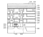
まず、図1乃至図5を参照して第1の実施例を説明する。
図1乃至図4は、キャパシタを有する半導体装置の製造工程を説明する工程断面図及び半導体基板上のキャパシタ平面図、図5は、図4に示すキャパシタの模式図である。本発明のシリコン半導体基板101に既存の技術を用いて素子分離領域102を形成し、例えば、半導体素子としてゲート電極103、ソース・ドレイン領域104等を順次形成してMOSトランジスタを設け、次いで、半導体基板101上に層間絶縁膜105をこのMOSトランジスタを被覆するように堆積させてこれを平坦化する。半導体基板上の配線は、ダマシン法などにより形成される。次に、層間絶縁膜105にビアホールを形成してこのビアホール内にコンタクト配線となる金属膜106を埋め込む。そして、その上に窒化シリコン膜107を形成し、この窒化シリコン膜107の上に多層配線層を構成する第1の配線層108を形成する。
【0016】
第1の配線層108は、Cuなどの金属膜とこの金属膜の側面及び底面を被覆するTiNなどのバリア層111とから構成されている。バリア層111は、金属膜が絶縁膜中に拡散するのを防止するために設けられている。金属配線層108は、バリア層(TiN)111を介して窒化シリコン膜107上に形成される層間絶縁膜(CVD−SiO2 )114中に埋め込まれている。金属配線層108は、銅などの金属を埋め込んだあとにダマシン法により加工することで形成されている。第1の配線層108は、コンタクト配線である金属膜106と電気的に接続されている。この層間絶縁膜114の上に窒化シリコン膜117を形成し、この窒化シリコン膜117の上に層間絶縁膜115を堆積させてこれを平坦化する。この層間絶縁膜115に第1の配線層108が露出するビアホール及び層間絶縁膜表面に開口部が形成された配線溝を形成し、このビアホール及び配線溝に金属膜を埋め込んで第1の配線層108と接続する第2の配線層109を形成する。第2の配線層109は、Cuなどの金属膜とこの金属膜の側面及び底面を被覆するTiNなどのバリア層112とから構成されている。
【0017】
層間絶縁膜115の上に窒化シリコン膜118を形成し、この窒化シリコン膜118の上に層間絶縁膜116を堆積させてこれを平坦化する。この層間絶縁膜116に第2の配線層109が露出するビアホール及び層間絶縁膜表面に開口部が形成された配線溝を形成し、このビアホール及び配線溝に金属膜を埋め込んで第2の配線層109と接続する第3の配線層110を形成する。第3の配線層110は、Cuなどの金属膜とこの金属膜の側面及び底面を被覆するTiNなどのバリア層113とから構成されている。層間絶縁膜116の上に窒化シリコン膜119を形成する。
次に、半導体基板101全面にチタン膜120、窒化チタン膜121、窒化シリコン膜122及び窒化チタン膜123を順次堆積させる。窒化チタン膜は、例えば、PVD(Physical Vapour Deposition)で形成される。窒化シリコン膜は、例えば、PVD、プラズマCVDなどで形成される(図1)。
【0018】
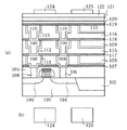
次に、窒化チタン膜123上にフォトレジスト(図示しない)を塗布し、これをパターニングし、このパターニングされたフォトレジストをマスクにして窒化チタン膜125をエッチングして(リソグラフィ技術)、窒化チタン膜123から1対の素子(第1の素子及び第2の素子)の上部電極124、125が形成される。
窒化チタン膜123をパターニングして形成された上部電極124及び上部電極125は、ほぼ同じ形状(即ち、実質的に両者は同じ面積である)である(図2)。
次に、全面にフォトレジスト(図示しない)を塗布して、公知のリソグラフィ技術及びRIE(Reactive Ion Etching)技術、アッシング技術により窒化シリコン膜122、窒化チタン膜121、チタン膜120を順次エッチングして、MIMキャパシタを構成する各層の処理が完了し、第1の素子のキャパシタ下部電極126と第2の素子のキャパシタ上部電極127が形成される。ここで形成されるキャパシタは、第1の素子とこの第1の素子と離れた位置に形成された第2の素子から構成される。
【0019】
第1の素子は、キャパシタ下部電極126−窒化シリコン膜(誘電体膜)122−キャパシタ上部電極124のキャパシタ構造を有し、第2の素子は、キャパシタ下部電極127−窒化シリコン膜(誘電体膜)122−キャパシタ上部電極125のキャパシタ構造を有している。第1及び第2の素子は、いずれもチタン膜120上に形成される。各素子のキャパシタ下部電極及び誘電体膜は、積層され、同じパターンである。また、それぞれのキャパ上部電極124、125は、いずれも誘電体膜及びキャパ下部電極が形成されている範囲の内側に設けられている。
【0020】
次に、酸化シリコン膜などの層間絶縁膜128がキャパシタを被覆するように形成されている(図3)。次に、半導体基板全面にフォトレジスト(図示せず)を塗布し、公知のリソグラフィ技術、RIE技術及びアッシング技術により、層間絶縁膜128にキャパシタ電極124、125、126、127に連通するコンタクトホールが形成される。続いて層間絶縁膜128全面に金属膜を形成し、更に金属膜全面にフォトレジスト(図示しない)を塗布し、公知のリソグラフィ技術、RIE技術及びアッシング技術により金属膜を加工して上層の配線層を形成する。このときの上層の配線層は、第1の素子のキャパシタ上部電極124と第2の素子のキャパシタ下部電極127とを接続する配線129、第1の素子のキャパシタ下部電極126と第2の素子のキャパシタ上部電極125とを接続する配線129′を有している(図4)。この実施例で形成される半導体装置は、さらに工程を進めて、配線129、129′及び層間絶縁膜128が被覆され表面が平坦化された絶縁膜(図示しない)が形成される。そして、その絶縁膜表面に接続パッドが形成され、保護膜が施されて製品化される。
【0021】
この様にして、半導体基板の多層配線層上に第1の素子及び第2の素子からなるキャパシタが形成される。その等価回路は、図5に示す通りである。このキャパシタは、上下対称でVCC1がほぼ0である。本発明のMIMキャパシタと通常のMIMキャパシタの製造工程の違いは、単にリソグラフィのマスクの相違のみであり、工程の変更や増加を伴わない。
なお、この実施例では誘電体膜としてシリコン窒化膜、電極膜として窒化チタン膜を用いたが、本発明は、これに限定されるものではなく、例えば、キャパシタ誘電体膜としてアルミナ膜、タンタルオキサイド膜、ハフニウムオキサイド膜、ジルコニウムオキサイド膜等の利用が可能であり、電極膜としても窒化タングステン膜、窒化タンタル膜、窒化チタン/AlCu/窒化チタン積層膜等の利用も可能である。また、例えば、誘電体膜としてタンタルオキサイド/アルミナ積層膜等の上下非対称な膜構造、あるいは上部電極が窒化チタン、下部電極が銅膜等の上下非対称な電極構造を用いてもVCC1をほぼ0にすることができる。
この実施例で形成される半導体装置のキャパシタは、例えば、アナログ−デジタルコンバータ(ADC)に用いられ、アナログ信号を入力してデジタル信号を出力する。この実施例では多層配線層は、3層であるが、本発明では層数に制限はない。
【0022】
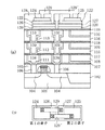
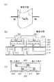
次に、図6を参照して第2の実施例を説明する。
図6は、半導体基板上の多層配線層の上に形成されたキャパシタの断面図、平面図及び模式図である。この図では半導体基板は示さず、多層配線層の上部及びその上に形成されたキャパシタを示している。この実施例では、比誘電率が20以上である高誘電率材料としてTa2 O5 をキャパシタ誘電体膜として用いることで高容量・高密度化をはかるものである。一般に、Ta2 O5 とTiN電極で形成されるMIMキャパシタは、リーク電流が大きい( リーク電流はキャパシタに蓄積された電荷損失によってVCC1と同様の信号の歪みをもたらす) という欠点があるので、従来はリーク電流を抑制する目的で電極の一方とTa2 O5 膜との間にAl2 O3 膜を挟み込んで絶縁性を改善している。
しかし、この構造では図6(a)に示すようにキャパシタ誘電体膜が積層構造で非対称な構造DEあるためにVCC1が約1000ppmと大きかった。そこで本発明の構造(即ち、積層構造が同じで上部電極の形状が同一の2つのキャパシタを用意し、それぞれの上部電極と相手の下部電極とをそれぞれ電気的に接続してこれらキャパシタを1つのキャパシタとする構造)を採用することによりVCC1をほぼ0にしながら、しかも低リーク電流化を実現することができた。
なお、MIMキャパシタ下地となる半導体基板上の多層配線層の形成工程は第1の実施例と同じであるので説明を省略する。
【0023】
第1の実施例と同様、MIMキャパシタは、多層金属配線層上に形成される。最上層の金属配線層110はバリア層(TiN)113を介して層間絶縁膜(CVDSiO2 )116中に埋め込まれている。金属配線層は、銅などの金属を埋め込んだあとにダマシン法により加工することで形成されている。金属配線層上には窒化シリコン層119が形成されている。
次に、半導体基板全面にチタン膜220、窒化チタン膜を形成し、その後、ALD(Atomic Layer Deposition )法によりAl2 O3 膜221を形成し、更にLPCVD法によりTa2 O5 膜222、スパッタ法により上部電極として成形される窒化チタン膜を順次形成する。次に、第1の実施例と同様に、積層された膜を加工して、第1及び第2の素子からなる一対のキャパシタを形成する。その後、層間絶縁膜228を形成後、配線工程において、第1の素子のキャパシタ上部電極224と第2の素子のキャパシタ下部電極227、第1の素子のキャパシタ下部電極226と第2の素子のキャパシタ上部電極225とがそれぞれ独立の配線229、229′で接続することにより、上下対称な構造を有するMIMキャパシタが形成される。配線229、229′は、キャパシタの上に層間絶縁膜228を介して形成された上層の金属配線層を構成している( 図6(b)) 。
【0024】
なお、この実施例ではリーク電流を抑制するためにAl2 O3 膜を用いたが、本発明は、この材料に限定されるものではなく、SiO2 、SiNx (x=1〜1.33)等の絶縁膜を用いることも可能である。
なお、この実施例では、比誘電率が20以上である高誘電率材料としてTa2 O5 膜を用いたが、本発明は、この材料に限定されるものではなく、Nb2 O3 、ZrO2 、HfO2 、La2 O3 、Pr2 O3 などの高誘電率材料を用いることができる。
【0025】
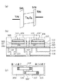
次に、図7を参照して第3の実施例を説明する。
図7は、半導体基板上の多層配線層の上に形成されたキャパシタの断面図、平面図及び模式図である。この図では半導体基板は示さず、多層配線層の上部及びその上に形成されたキャパシタを示している。この実施例では、比誘電率が20以上の高誘電率材料であるTa2 O5 の上下をSiN膜で挟み込んだ構造のキャパシタ誘電体膜として用いるMIMキャパシタ上下のSiN膜の膜厚が異なることに起因するVCC1成分を本発明の構造によって抑制するものである。第2の実施例ではリーク電流を抑制するために下部電極側にTa2 O5 と別の絶縁膜を挟み込む構造であったが、125℃などの高温で動作を保証するLSI用途ではリーク電流抑制のためにTa2 O5 の上下に絶縁膜を挟み込む必要が生じる。リーク電流低減のための絶縁膜は、一般にTa2 O5 に比べて低誘電率であるために高容量密度化を実現するにはその膜厚を可能な限り薄くした方がよい。下部電極側に比べて上部電極側の絶縁膜は上部電極スパッタ時のプラズマダメージを受けるため、下部電極側と同等のリーク電流抑制効果を得るためには厚膜化する必要がある。例えば、PVDで形成するSiNを上部電極とTa2 O5 との界面に5nm、Ta2 O5 と下部電極との界面に2nm挿入することで、125℃±3.6Vで1.0×10⁻¹⁰ A/mm2 以下の低リーク電流が実現できた。
【0026】
しかし、この構造では図7(a)に示すようにキャパシタ誘電体膜が積層構造で非対称な構造をしているためにVCC1が約600ppmと大きかった。そこで、本発明の構造を採用することにより、VCC1をほぼ0にしながら低リーク電流を実現することができた。
MIMキャパシタを支持する半導体基板上の多層金属配線層の形成工程は第1の実施例と同じなので説明を省略する。
MIMキャパシタは多層金属配線層上に形成される。最上層の金属配線層110はバリア層113を介して層間絶縁膜116中に埋め込まれている。金属配線層は銅などの金属を埋め込んだあとにダマシン法などにより加工することで形成されている。配線層上には窒化シリコン層119が形成されている。
【0027】
次に、半導体基板全面にチタン膜320、窒化チタン膜を形成したあとに、スパッタリング法によりSiN膜321、Ta2 O5 膜322、SiN膜323、上部電極となる窒化チタン膜を順次形成する。次に、第1及び第2の実施例と同様に、第1の素子及び第2の素子からなる一対のキャパシタを加工し、層間絶縁膜328の形成と配線とを行うことにより、MIMキャパシタを形成する。ここで第1の素子のキャパシタ上部電極324と第2の素子のキャパシタ下部電極327、第1の素子のキャパシタ下部電極326と第2の素子のキャパシタ上部電極325とがそれぞれ独立の配線329、329′で接続されることにより、上下対称な構造を有するMIMキャパシタが形成される。配線329、329′は、キャパシタの上に層間絶縁膜328を介して形成された上層の金属配線層を構成している(図7(b))。
なお、ここではリーク電流を抑制するためにSiN膜を用いたが、本発明は、SiO2 、ZrO2 、HfO2 、La2 O3 、Pr2 O3 等の絶縁膜を用いることも可能である。また、SiN、Ta2 O5 膜形成にはスパッタリング法を用いたが、本発明は、CVD法あるいは塗布法による形成も可能である。
【0028】
次に、図8を参照して第4の実施例を説明する。
図8は、半導体基板上の多層配線層の上に形成されたキャパシタの断面図、平面図及び模式図である。この図では半導体基板は示さず、多層配線層の上部及びその上に形成されたキャパシタを示している。この実施例では比誘電率が20以上の高誘電率材料であるTa2 O5 を用いるMIMキャパシタの上下電極としてNi電極を用いるものである。Ni電極/Ta2 O5 界面は、熱的に安定なので第2乃至第3の実施例に示したようなSiNなどのバリア層は不要であり、容易に低リーク電流を得ながら、なおかつ非常に高い容量密度(30nmのTa2 O5 で〜7fF/μm2 、Ta2 O5 と電極との界面に低誘電率材料を挿入する構造では4fF/μm2 程度が高容量密度化の限界である) が得られるが、VCC1を評価したところ800ppmと大きかった。これは、とくに上部電極のNiをスパッタリングで形成する際に、Ta2 O5 膜中にプラズマダメージによる欠陥( 酸素欠損) が生じる。図8(a)及び図8(b)では酸素欠損を“×”で模式的に示している。酸素欠損は、2価のドナーとして働くので、エネルギーバンドは湾曲し、バンド構造の上下対称性が崩れるためにVCC1が増大する。しかし、本発明の構造を採用することにより、VCC1をほぼ0にしながら低リーク電流と高容量密度とを実現することができる。
【0029】
MIMキャパシタを支持する半導体基板上の多層配線層の形成工程は、第1の実施例と同じなので説明を省略する。
MIMキャパシタは、多層金属配線層上に形成される。最上層の金属配線層110は、バリア層113を介して層間絶縁膜116中に埋め込まれている。金属配線層は銅などの金属を埋め込んだあとにダマシン法により加工することで形成されている。配線層上には窒化シリコン層119が形成されている。
【0030】
次に、半導体基板上の窒化シリコン膜119全面にスパッタリング法により下部電極となるニッケル(Ni)膜401、Ta2 O5 膜402、上部電極となるニッケル(Ni)膜403を順次形成する。次に、第1乃至第3の実施例と同様に、第1の素子と第2の素子からなる一対のキャパシタを加工し、層間絶縁膜408の形成と配線接続とを行うことにより、MIMキャパシタを形成する。ニッケル(Ni)膜401は、第1及び第2の素子の下部電極406、407に加工され、Ta2 O5 膜402は、第1及び第2の素子の誘電体膜に加工され、ニッケル(Ni)膜403は、第1及び第2の素子の上部電極404、405に加工される。ここで、第1の素子のキャパシタ上部電極404と第2の素子のキャパシタ下部電極406、第1の素子のキャパシタ下部電極405と第2の素子のキャパシタ上部電極404とがそれぞれ独立の配線409、409′で接続することにより、上下対称な構造を有するMIMキャパシタが形成される。配線409、409′は、キャパシタの上に層間絶縁膜408を介して形成された上層の金属配線層を構成している(図8(b))。
【0031】
次に、図9を参照して第5の実施例を説明する。
図9は、半導体基板上の多層配線層の上に形成されたキャパシタの断面図、平面図及び模式図である。この図では半導体基板は示さず、多層配線層の上部及びその上に形成されたキャパシタを示している。この実施例は、上部及び下部電極に異種材料を用いることによる非対称性を本発明により相殺するものである。MIMキャパシタの電極は、低抵抗であるほど回路特性(Q値)が向上するので低抵抗であることが望ましい。低抵抗の電極として半導体装置(LSI)の多層配線に用いられる銅(Cu)は有望であり、配線層形成時にMIMキャパシタの下部電極が同時に形成できるという製造上の利点もある。しかし、Cuの加工は通常ダマシン法で形成されており、MIMキャパシタの上部電極には用い難い。何故ならMIMキャパシタの上部電極加工は通常RIE技術を用いて行うからである。そこで上部電極には従来用いてきたTiNを用いると、SiNとTiN、SiNとCuとの間のショットキーバリア高さが異なるために、図9(a)に示すように、エネルギーバンドは非対称な構造になり、VCC1の値は約180ppmとなった。
そこで、本発明の構造を採用することにより、VCC1をほぼ0にしながら良好なQ値が得られるMIMキャパシタを実現できた。
【0032】
半導体基板及びMIMキャパシタを支持する多層金属配線層の形成工程は、第1の実施例と同じなので説明を省略する。
この実施例のMIMキャパシタの下部電極505は、多層金属配線層の最上層の金属配線層110の一部を兼用することを特徴としている。金属配線層110は、バリア層113を介して層間絶縁膜116中に埋め込まれている。金属配線層は銅などの金属を埋め込んだあとにダマシン法により加工することで形成されている。
次に、スパッタリング法により一部が下部電極となる多層金属配線層の最上層の金属配線層110上及び層間絶縁膜116上に窒化シリコン膜501、上部電極となる窒化チタン膜502を順次形成する。次に、第1乃至第4の実施例と同様に、第1の素子及び第2の素子からなる一対のキャパシタが形成されるように窒化チタン膜502を加工し、層間絶縁膜508の形成と配線とを行うことによりMIMキャパシタが形成される。ここで、最上層の金属配線層110は、一部を第1及び第2の素子の下部電極505、506として用いられる。そして、その上の窒化シリコン膜501は、第1及び第2の素子の誘電体膜として共用される。さらに、窒化チタン膜502は、誘電体膜を介して下部電極505、506上にそれぞれ載置される上部電極503、504に加工される。
【0033】
ここで、第1の素子のキャパシタ上部電極503と第2の素子のキャパシタ下部電極506、第1の素子のキャパシタ下部電極505と第2の素子のキャパシタ上部電極504とがそれぞれ独立の配線509、509′で接続することにより、上下対称な構造を有するMIMキャパシタが形成される。配線509、509′は、キャパシタの上に層間絶縁膜508を介して形成された上層の金属配線層を構成している(図9(b))。
以上の実施例ではSiN膜はスパッタリング法で形成した。これは、上部電極である窒化チタンも連続にスパッタリングで形成できるので製造時間短縮に有効であるからである。しかし、本発明は、スパッタリングに代えてSiNを通常のPECVD(プラズマCVD)法で形成することも可能である。
本発明は、以上のような構成により、半導体基板上のキャパシタが上下対称な構造にあるためVCC1をほぼ0にすることができる。したがって、キャパシタに入力するアナログ信号は歪みのないデジタル信号となって出力される。
【0034】
また、プロセスダメージ等に起因して発生するキャパシタ絶縁膜中の欠陥が上下電極界面に対称に存在しない場合であってもVCC1への寄与が相殺される。この効果はプロセスダメージ除去のための熱処理が事実上不可能な多層配線層上のMIMキャパシタに対して極めて有効である。
また、通常、MIMキャパシタの配線はMIMキャパシタの面積が極めて大きいので下部電極への配線と上部電極への配線の長さが異なり、インダクタンスも大きく異なるために回路のQ値が悪化する傾向にある。本発明のように一対のキャパシタの各電極間を接続する配線を上層の配線層を介してとることによりキャパシタ電極に接続される配線のインダクタンスをほぼ等しくすることが可能になるので回路のQ値向上に有効である。
また、本発明の構造を採用しても製造工程の数は増大しない。MIMキャパシタの面積はもともと数百ミクロンオーダーと大きいのに対して、現在のCMOSの加工寸法は0.1ミクロンオーダーの加工が容易にできるので、本発明の構造を採用しても半導体装置面積への影響は殆ど認められない。
【0035】
【発明の効果】
以上、本発明は、半導体基板上のキャパシタが上下対称な構造にあるためVCC1をほぼ0にすることができる。したがって、キャパシタに入力するアナログ信号は歪みのないデジタル信号となって出力される。
【図面の簡単な説明】
【図1】本発明に係る第1の実施例の半導体装置の製造工程を説明する工程断面図。
【図2】本発明に係る第1の実施例の半導体装置の製造工程を説明する工程断面図及び半導体基板上のキャパシタの平面図。
【図3】本発明に係る第1の実施例の半導体装置の製造工程を説明する工程断面図及び半導体基板上のキャパシタの平面図。
【図4】本発明に係る第1の実施例の半導体装置の製造工程を説明する工程断面図及び半導体基板上のキャパシタの平面図。
【図5】図4の半導体基板に形成されたキャパシタの模式図。
【図6】本発明に係る第2の実施例の半導体装置の断面図及び半導体基板上のキャパシタの平面図及びキャパシタ模式図。
【図7】本発明に係る第3の実施例の半導体装置の断面図及び半導体基板上のキャパシタの平面図及びキャパシタ模式図。
【図8】本発明に係る第4の実施例の半導体装置の断面図及び半導体基板上のキャパシタの平面図及びキャパシタ模式図。
【図9】本発明に係る第5の実施例の半導体装置の断面図及び半導体基板上のキャパシタの平面図及びキャパシタ模式図。
【図10】ADコンバータの動作原理を示す模式図。
【符号の説明】
101・・・半導体基板
102・・・素子分離領域
103・・・ゲート電極
104・・・ソース・ドレイン領域
105、114、115、116、128、228、328、408、508・・・層間絶縁膜
106・・・金属膜
107、117、118、119、122、321、323、501・・・窒化シリコン膜(SiN)
108、109、110・・・金属配線層
111、112、113・・・バリア層
120、220、320・・・チタン膜
121、123、502・・・窒化チタン膜
124、125、224、225、324、325、404、405、503、504・・・キャパシタ上部電極
126、127、226、227、326、327、406、407、505、506・・・キャパシタ上部電極
129、129′、229、229′、329、329′、409、409′、509、509′・・・配線
221・・・Al2 O3 膜
222、322、402・・・Ta2 O5 膜
401、403・・・ニッケル(Ni)膜
601・・・キャパシタ
602、603・・・スイッチング素子[0001]
TECHNICAL FIELD OF THE INVENTION
The present invention relates to a semiconductor device provided with an MIM (Metal-Insulator-Metal) capacitor used for RF communication and the like.
[0002]
[Prior art]
With the development of communication technology, personal computers (PCs) and personal digital assistants (PDAs) are rarely used in a stand-alone manner, and are commonly used connected to a network. In the future, home appliances such as refrigerators and air conditioners are expected to be connected to the network. When a network is formed by such a large number of devices, especially in ordinary households, a method of constructing a network by wiring a LAN cable between individual devices conventionally performed in an office or the like is not suitable. Wireless connection using wireless is expected to become the mainstream in the future. Therefore, it is conceivable that an RF communication function will be added to most LSI chips in the future. Conventionally, an LSI used for such an application has been constituted by a plurality of chips (RF analog device (SiGe-BiCMOS or the like) and a CMOS logic device) according to the application. Therefore, since it is required to realize a desired circuit performance with a smaller printed circuit board occupation area, further miniaturization by an RF embedded LSI is required.
[0003]
In addition, in order to make it easier for equipment manufacturers to use RF communication, RF analog devices and CMOS logic devices are mixed in a single chip. There is a need to make functions available.
On the other hand, in order to integrate the RF analog device and the CMOS logic device into one chip, it is necessary to integrate the manufacturing processes of both devices. The RF analog device includes a resistor, an inductance, a capacitor, and the like, and the CMOS logic device includes a MOS transistor. Therefore, in order to realize an embedded LSI, it is necessary to develop a new RF-CMOS process based on, for example, a CMOS logic process and integrating the process of an RF analog device.
[0004]
In integrating the two processes, the first problem is the structure and process of the capacitor. In order to mix RF analog circuits, it is necessary to mix capacitors for a plurality of purposes, and the specifications required for each purpose are different. However, this is a single specification (capacity density per unit area). , A leakage current characteristic, etc.). For example, while only a voltage of several tens of microvolts is applied to a capacitor used for a noise filter of an RF receiving unit, a voltage of 2.5 to 3.6 volts is applied to an analog-to-digital converter (AD converter). You.
[0005]
Therefore, a capacitor mounted on an analog circuit is required to be a highly insulating capacitor capable of realizing a low leakage current even when used at several tens of microvolts or at about 3 volts. . In addition, requirements for linearity (Voltage Linearity) of the amount of charge stored in the capacitor with respect to the applied voltage differ depending on the purpose. Although the linearity is not important for the above-described noise filter application, very good linearity is required for the AD converter. This is because the AD converter is typically composed of one
[0006]
In general, the amount of charge Q stored in a capacitor is given by a capacitance C and an applied voltage V.
Q = CV (1)
Is represented by the relationship C is usually regarded as a constant, but actually has a weak perturbation term shown in the equation (2).
Q = CV = C 0 (1 + VCC1 × V + VCC2 × V 2 ) (2)
In an ideal system, VCC1 = VCC2 = 0. When VCC1 = VCC2 = 0, the charge written to the capacitor 201 is converted into a digital signal without distorting the waveform. However, when VCC1 or VCC2 is not 0, the waveform is distorted particularly at a portion where the amplitude of the RF waveform is large. Will be digitally converted. Particularly, compared to VCC2, VCC1 greatly distorts the waveform even near 0 volts, so that the effect on the AD converter performance is great. Therefore, the capacitor built in the RF embedded circuit is depleted in the silicon electrode in a MOS (Metal-Oxide-Semiconductor) capacitor or a PIP (Poly-Si-Insulator-Poly-Si) capacitor which has been widely used in a semiconductor device. Therefore, the MIM capacitor must be a MIM capacitor in which electrode depletion cannot occur.
[0007]
That is, in order to realize the RF embedded LSI, a very high performance MIM capacitor is required. On the other hand, there is always a demand for LSI miniaturization and chip area reduction. In the case of MIM capacitors, since the area of each capacitor is as large as several hundred square microns, the capacitor area can be reduced, that is, the capacitance of the capacitor per unit area can be reduced. Improvement becomes very important. However, in order to improve the capacitance density of such a large-capacity capacitor, it is necessary to increase the effective capacitor surface area by making the electrodes three-dimensional and using the side area, which has been conventionally used in DRAM capacitors and the like. It is difficult to increase the capacitance per projected area. Because, in order to increase the side area corresponding to the huge projected area, the method of simply processing the electrode in a column shape and using the side area requires an electrode with a height of several tens of microns, which is impractical. Therefore, a complicated processing step for forming fine irregularities on the electrode surface is required.
For this purpose, the use of high dielectric constant materials such as alumina and tantalum oxide in place of the silicon nitride film conventionally used as the dielectric of the MIM capacitor has been studied, and some commercial production has begun. ing.
[0008]
By the way, if the capacitor for the RF embedded circuit can be formed on the multilayer wiring on the semiconductor substrate, there is an advantage that the process is simplified and the distance from the semiconductor substrate is increased, so that the parasitic capacitance to the ground is reduced. Alternatively, the upper limit of the forming temperature of the MIM capacitor is about 400 ° C. at the cost of being formed on the aluminum multilayer wiring. The limitation on the upper limit of the process temperature makes it difficult to form a high-permittivity film having a high quality. (When a high-permittivity material is considered as a gate insulating film, a heat process at 800 ° C. or higher causes defects in the film. (Usually used for removal), indicating that defects formed in the high dielectric constant material due to process damage cannot be removed by heat treatment.
It should be noted that Patent Documents 1 and 2 disclose that a capacitor formed on a semiconductor substrate has a structure with low voltage dependency.
[0009]
[Patent Document 1]
JP-A-59-55047 (FIGS. 4 and 5, page 5)
[Patent Document 2]
JP-A-1-241858 (FIGS. 1 and 2, page 2)
[0010]
[Problems to be solved by the invention]
The damage caused by such a process includes, for example, plasma damage applied to a high dielectric constant material having a relative dielectric constant of 20 or more when the capacitor upper electrode is formed by a sputtering method, and high damage when processing the capacitor upper electrode. Etching damage to the dielectric constant film, plasma damage when the capacitor is covered with an interlayer insulating film formed by plasma CVD (Chemical Vapor Deposition), generation of oxygen deficiency due to a reducing atmosphere, and the like can be increased.
It is also considered that the reaction with the metal film of the lower electrode (most typical reduction of the high dielectric material by the lower electrode metal) occurs during the deposition of the high dielectric material, as process-induced damage. In particular, the damage caused by the plasma process has a close correlation with the distribution of the plasma on the semiconductor substrate, and when the plasma is formed on a 300 mmφ substrate as in a current CMOS device, it is not possible to cause uniform damage in the substrate surface. Unexpected, damage itself has a normal distribution. Therefore, it has been very difficult to produce a high-dielectric-constant MIM capacitor having good linearity with respect to an applied voltage over the entire surface of a large-diameter substrate.
The present invention is a high-capacity, high-density MIM capacitor suitable for forming on multilayer wiring on a semiconductor substrate, and a capacitor exhibiting good linearity with respect to an applied voltage suitable for application to an analog circuit such as an AD converter. provide.
[0011]
[Means for Solving the Problems]
According to the present invention, in a semiconductor device including an MIM capacitor, the MIM capacitor is composed of a pair of capacitors having substantially the same area, and a lower electrode of one capacitor and an upper electrode of the other capacitor are interconnected with each other. It is characterized by having an electrically connected structure. With such a structure, a capacitor having extremely excellent linearity with respect to voltage is realized.
For example, a film forming method in which a reaction at an electrode interface easily occurs, for example, a high dielectric constant material having a relative dielectric constant of 20 or more or a uniform interface formation on a large-area substrate is difficult (for example, many plasmas such as sputtering and plasma CVD) Process), it is possible to ensure good linearity with respect to the applied voltage, so that it will contribute to the reduction of the area of RF-embedded LSIs that will be installed in all types of devices in the future, and eventually to the miniaturization of these devices. Becomes possible.
[0012]
That is, the semiconductor device of the present invention includes a semiconductor substrate on which a semiconductor element is formed, a multilayer metal wiring layer in which a plurality of layers are stacked on the semiconductor substrate via an interlayer insulating film, and A capacitor formed of an upper metal electrode, a dielectric film, and a lower metal electrode formed with an interlayer insulating film interposed therebetween, and an upper wiring layer provided on the insulating film formed so as to cover the capacitor; Wherein the capacitor comprises a first and a second element, and the first and the second elements each comprise a laminated lower metal electrode, a dielectric film and an upper metal electrode, and each upper metal The electrodes are substantially the same size and shape, and each upper metal electrode is formed in a region where the lower metal electrode and the dielectric film are formed and arranged, respectively, and a lower portion of the first element is formed. The metal electrode and the upper metal electrode of the second element are electrically connected, and the upper metal electrode of the first element and the lower metal electrode of the second element are electrically connected. It is a feature (claim 1). The lower metal electrode of the first element and the upper metal electrode of the second element are connected by a first wiring forming the upper wiring layer, and the upper metal electrode of the first element and the second metal electrode are connected to each other. The element may be connected to the lower metal electrode by a second wiring constituting the upper wiring layer (claim 2).
[0013]
The dielectric film constituting the capacitor may be formed of a laminated film composed of a first film made of a high dielectric material and a second film made of a material having low leakage current. ). The dielectric film constituting the capacitor is a laminated film composed of a first film made of a high dielectric material and a second and a third film sandwiching the first film, made of a material having a low leakage current. (Claim 6). The dielectric film forming the capacitor may have oxygen deficiency, and the upper metal electrode and the lower metal electrode forming the capacitor may be made of nickel.
[0014]
The semiconductor device of the present invention includes a semiconductor substrate on which a semiconductor element is formed, a multilayer metal wiring layer in which a plurality of layers are stacked on the semiconductor substrate via an interlayer insulating film, and the multilayer metal wiring on the semiconductor substrate. A dielectric film formed so as to cover the layers, first and second upper metal electrodes having substantially the same size and shape formed on the dielectric film, and the first and second upper electrodes; An upper wiring layer provided on an insulating film formed so as to cover the metal electrode and the dielectric film, wherein the first and second upper metal wirings, the dielectric film and the multilayer metal wiring layer are provided. The uppermost metal wiring layer forms a capacitor, and the capacitor includes first and second elements. The first element includes the first upper metal electrode, the dielectric film, and the first element. A first lower metal part of an upper metal wiring layer The second element is composed of the second upper metal electrode, the dielectric film, and a second lower metal electrode composed of part of the uppermost metal wiring layer. 2 upper metal electrodes are formed in regions where the first lower metal electrode, the second lower electrode, and the dielectric film are formed and arranged, respectively, and the first lower metal electrode of the first element is formed. The electrode and the second upper metal electrode of the second element are electrically connected, and the first upper metal electrode of the first element and the second lower metal electrode of the second element are electrically connected. (Claim 13). A first lower metal electrode of the first element and a second upper electrode of the second element are connected by a first wiring constituting the upper wiring layer, and a first wiring of the first element is provided. The upper metal electrode and the second lower metal electrode of the second element may be connected by a second wiring constituting the upper wiring layer (claim 15).
[0015]
BEST MODE FOR CARRYING OUT THE INVENTION
Hereinafter, embodiments of the present invention will be described with reference to the drawings.
First, a first embodiment will be described with reference to FIGS.
1 to 4 are process cross-sectional views illustrating a manufacturing process of a semiconductor device having a capacitor and plan views of the capacitor on a semiconductor substrate. FIG. 5 is a schematic diagram of the capacitor shown in FIG. An
[0016]
The
[0017]
A
Next, a
[0018]
Next, a photoresist (not shown) is applied on the
The
Next, a photoresist (not shown) is applied to the entire surface, and the
[0019]
The first element has a capacitor structure of a capacitor lower electrode 126-a silicon nitride film (dielectric film) 122-a capacitor
[0020]
Next, an interlayer insulating film 128 such as a silicon oxide film is formed so as to cover the capacitor (FIG. 3). Next, a photoresist (not shown) is applied to the entire surface of the semiconductor substrate, and contact holes communicating with the
[0021]
In this way, a capacitor including the first element and the second element is formed on the multilayer wiring layer of the semiconductor substrate. The equivalent circuit is as shown in FIG. This capacitor is vertically symmetrical and VCC1 is almost 0. The difference between the manufacturing process of the MIM capacitor of the present invention and a normal MIM capacitor is only a difference in a lithography mask, and does not involve a change or an increase in processes.
In this example, a silicon nitride film was used as the dielectric film and a titanium nitride film was used as the electrode film. However, the present invention is not limited to this. For example, an alumina film, a tantalum oxide A film, a hafnium oxide film, a zirconium oxide film, or the like can be used. As an electrode film, a tungsten nitride film, a tantalum nitride film, a titanium nitride / AlCu / titanium nitride laminated film, or the like can be used. For example, even if a vertically asymmetric film structure such as a tantalum oxide / alumina laminated film as a dielectric film, or a vertically asymmetric electrode structure such as a titanium nitride as an upper electrode and a copper film as a lower electrode is used, VCC1 becomes almost zero. can do.
The capacitor of the semiconductor device formed in this embodiment is used, for example, in an analog-to-digital converter (ADC), and inputs an analog signal and outputs a digital signal. Although the number of multilayer wiring layers is three in this embodiment, the number of layers is not limited in the present invention.
[0022]
Next, a second embodiment will be described with reference to FIG.
FIG. 6 is a sectional view, a plan view, and a schematic view of a capacitor formed on a multilayer wiring layer on a semiconductor substrate. In this figure, the semiconductor substrate is not shown, but the upper part of the multilayer wiring layer and the capacitors formed thereon are shown. In this embodiment, Ta is used as a high dielectric constant material having a relative dielectric constant of 20 or more. 2 O 5 Is used as a capacitor dielectric film to achieve high capacity and high density. Generally, Ta 2 O 5 The MIM capacitor formed of the Nb and TiN electrodes has a disadvantage that the leakage current is large (the leakage current causes the same signal distortion as VCC1 due to the charge loss stored in the capacitor). Ta and one of the electrodes for the purpose 2 O 5 Al between the film 2 O 3 The insulation is improved by sandwiching the film.
However, in this structure, VCC1 was as large as about 1000 ppm because the capacitor dielectric film had a laminated structure and an asymmetric structure DE as shown in FIG. 6A. Accordingly, two capacitors having the same laminated structure and the same upper electrode shape are prepared according to the structure of the present invention, and each upper electrode and the other lower electrode are electrically connected to each other to form one capacitor. By adopting a capacitor structure, it is possible to reduce the leakage current while making VCC1 almost zero.
Note that the steps of forming the multilayer wiring layer on the semiconductor substrate serving as the base of the MIM capacitor are the same as those in the first embodiment, and a description thereof will be omitted.
[0023]
As in the first embodiment, the MIM capacitor is formed on the multilayer metal wiring layer. The uppermost
Next, a
[0024]
In this embodiment, in order to suppress the leakage current, Al 2 O 3 Although a film was used, the present invention is not limited to this material. 2 , SiN x It is also possible to use an insulating film such as (x = 1 to 1.33).
In this example, Ta was used as a high dielectric constant material having a relative dielectric constant of 20 or more. 2 O 5 Although a film was used, the present invention is not limited to this material. 2 O 3 , ZrO 2 , HfO 2 , La 2 O 3 , Pr 2 O 3 For example, a high dielectric constant material such as
[0025]
Next, a third embodiment will be described with reference to FIG.
FIG. 7 is a sectional view, a plan view, and a schematic view of a capacitor formed on a multilayer wiring layer on a semiconductor substrate. In this figure, the semiconductor substrate is not shown, but the upper part of the multilayer wiring layer and the capacitors formed thereon are shown. In this embodiment, Ta is a high dielectric constant material having a relative dielectric constant of 20 or more. 2 O 5 The VCC1 component caused by different thicknesses of the upper and lower SiN films used as a capacitor dielectric film having a structure in which the upper and lower sides of the MIM capacitor are sandwiched between SiN films is suppressed by the structure of the present invention. In the second embodiment, in order to suppress the leak current, 2 O 5 However, in LSI applications that guarantee operation at high temperatures such as 125 ° C., Ta is used to suppress leakage current. 2 O 5 It is necessary to sandwich an insulating film above and below. An insulating film for reducing leakage current is generally made of Ta. 2 O 5 Since the dielectric constant is lower than that of the above, it is better to make the film thickness as thin as possible in order to realize a higher capacity density. Since the insulating film on the upper electrode side is more damaged by plasma at the time of sputtering the upper electrode than on the lower electrode side, it is necessary to increase the thickness of the insulating film in order to obtain the same leak current suppressing effect as on the lower electrode side. For example, SiN formed by PVD is used as an upper electrode and Ta. 2 O 5 5nm, Ta at the interface with 2 O 5 By inserting 2 nm at the interface between the substrate and the lower electrode, 1.0 × 10 5 at 125 ° C. ± 3.6 V -10 A / mm 2 The following low leakage current was realized.
[0026]
However, in this structure, VCC1 was as large as about 600 ppm because the capacitor dielectric film had a laminated and asymmetric structure as shown in FIG. 7A. Then, by adopting the structure of the present invention, it was possible to realize a low leakage current while making VCC1 almost zero.
The process of forming the multilayer metal wiring layer on the semiconductor substrate supporting the MIM capacitor is the same as that of the first embodiment, and the description is omitted.
The MIM capacitor is formed on the multilayer metal wiring layer. The uppermost
[0027]
Next, after forming a
Although a SiN film was used here to suppress the leakage current, the present invention 2 , ZrO 2 , HfO 2 , La 2 O 3 , Pr 2 O 3 It is also possible to use such an insulating film. Also, SiN, Ta 2 O 5 Although the film is formed by the sputtering method, the present invention can also be formed by a CVD method or a coating method.
[0028]
Next, a fourth embodiment will be described with reference to FIG.
FIG. 8 is a sectional view, a plan view, and a schematic view of a capacitor formed on a multilayer wiring layer on a semiconductor substrate. In this figure, the semiconductor substrate is not shown, but the upper part of the multilayer wiring layer and the capacitors formed thereon are shown. In this embodiment, Ta, which is a high dielectric constant material having a relative dielectric constant of 20 or more, is used. 2 O 5 In this case, Ni electrodes are used as upper and lower electrodes of a MIM capacitor using the above method. Ni electrode / Ta 2 O 5 Since the interface is thermally stable, a barrier layer such as SiN as shown in the second and third embodiments is unnecessary, and a very high capacitance density (Ta of 30 nm) can be obtained while easily obtaining a low leakage current. 2 O 5 ~ 7fF / μm 2 , Ta 2 O 5 4fF / μm for a structure in which a low dielectric material is inserted at the interface between 2 The degree is the limit of increasing the capacity density), but when VCC1 was evaluated, it was as large as 800 ppm. This is especially true when the upper electrode Ni is formed by sputtering. 2 O 5 Defects (oxygen deficiency) occur in the film due to plasma damage. 8 (a) and 8 (b), oxygen vacancies are schematically indicated by "x". Since oxygen vacancy acts as a bivalent donor, the energy band is curved, and the vertical symmetry of the band structure is lost, so that VCC1 increases. However, by employing the structure of the present invention, it is possible to realize a low leakage current and a high capacity density while making VCC1 almost zero.
[0029]
The step of forming the multilayer wiring layer on the semiconductor substrate supporting the MIM capacitor is the same as that of the first embodiment, and the description is omitted.
The MIM capacitor is formed on the multilayer metal wiring layer. The uppermost
[0030]
Next, a nickel (Ni)
[0031]
Next, a fifth embodiment will be described with reference to FIG.
FIG. 9 is a sectional view, a plan view, and a schematic view of a capacitor formed on a multilayer wiring layer on a semiconductor substrate. In this figure, the semiconductor substrate is not shown, but the upper part of the multilayer wiring layer and the capacitors formed thereon are shown. In this embodiment, the asymmetry caused by using different materials for the upper and lower electrodes is canceled by the present invention. The electrode of the MIM capacitor desirably has a low resistance because the lower the resistance, the better the circuit characteristics (Q value). Copper (Cu), which is used as a low-resistance electrode in a multilayer wiring of a semiconductor device (LSI), is promising, and has an advantage in manufacturing that a lower electrode of a MIM capacitor can be formed simultaneously when a wiring layer is formed. However, Cu is usually formed by a damascene method, and is difficult to use for the upper electrode of the MIM capacitor. This is because the processing of the upper electrode of the MIM capacitor is usually performed using the RIE technique. Therefore, when the conventionally used TiN is used for the upper electrode, the Schottky barrier heights between SiN and TiN and between SiN and Cu are different, so that the energy band is asymmetric as shown in FIG. The structure was obtained, and the value of VCC1 was about 180 ppm.
Therefore, by adopting the structure of the present invention, it was possible to realize a MIM capacitor which can obtain a good Q value while making VCC1 almost zero.
[0032]
The steps of forming the multi-layered metal wiring layer supporting the semiconductor substrate and the MIM capacitor are the same as those in the first embodiment, and a description thereof will be omitted.
The
Next, a
[0033]
Here, the capacitor
In the above embodiment, the SiN film was formed by the sputtering method. This is because titanium nitride as the upper electrode can be continuously formed by sputtering, which is effective in shortening the manufacturing time. However, in the present invention, SiN can be formed by ordinary PECVD (plasma CVD) instead of sputtering.
According to the present invention, since the capacitor on the semiconductor substrate has a vertically symmetric structure with the above-described configuration, VCC1 can be made substantially zero. Therefore, the analog signal input to the capacitor is output as a digital signal without distortion.
[0034]
Further, even when defects in the capacitor insulating film generated due to process damage or the like do not exist symmetrically at the interface between the upper and lower electrodes, the contribution to VCC1 is canceled. This effect is extremely effective for an MIM capacitor on a multilayer wiring layer where heat treatment for removing process damage is practically impossible.
In addition, the wiring of the MIM capacitor usually has an extremely large area of the MIM capacitor, so the length of the wiring to the lower electrode and the length of the wiring to the upper electrode are different. . Since the wiring connecting the electrodes of the pair of capacitors is taken through the upper wiring layer as in the present invention, the inductance of the wiring connected to the capacitor electrodes can be made substantially equal, so that the Q value of the circuit can be reduced. It is effective for improvement.
In addition, adopting the structure of the present invention does not increase the number of manufacturing steps. Although the area of the MIM capacitor is originally as large as several hundred microns, the current CMOS processing size can be easily processed to the order of 0.1 μm. Almost no effect is observed.
[0035]
【The invention's effect】
As described above, according to the present invention, since the capacitor on the semiconductor substrate has a vertically symmetric structure, VCC1 can be made substantially zero. Therefore, the analog signal input to the capacitor is output as a digital signal without distortion.
[Brief description of the drawings]
FIG. 1 is a process cross-sectional view for explaining a manufacturing process of a semiconductor device according to a first embodiment of the present invention.
FIG. 2 is a process cross-sectional view illustrating a manufacturing process of the semiconductor device according to the first embodiment of the present invention, and a plan view of a capacitor on a semiconductor substrate.
FIG. 3 is a process cross-sectional view illustrating a manufacturing process of the semiconductor device according to the first embodiment of the present invention, and a plan view of a capacitor on a semiconductor substrate.
FIG. 4 is a process cross-sectional view illustrating a manufacturing process of the semiconductor device according to the first embodiment of the present invention and a plan view of a capacitor on a semiconductor substrate.
FIG. 5 is a schematic diagram of a capacitor formed on the semiconductor substrate of FIG. 4;
FIG. 6 is a sectional view of a semiconductor device according to a second embodiment of the present invention, a plan view of a capacitor on a semiconductor substrate, and a schematic diagram of the capacitor.
FIG. 7 is a sectional view of a semiconductor device according to a third embodiment of the present invention, a plan view of a capacitor on a semiconductor substrate, and a schematic diagram of the capacitor.
FIG. 8 is a sectional view of a semiconductor device according to a fourth embodiment of the present invention, a plan view of a capacitor on a semiconductor substrate, and a schematic diagram of the capacitor.
FIG. 9 is a sectional view of a semiconductor device according to a fifth embodiment of the present invention, a plan view of a capacitor on a semiconductor substrate, and a schematic diagram of the capacitor.
FIG. 10 is a schematic diagram showing the operation principle of an AD converter.
[Explanation of symbols]
101 ... semiconductor substrate
102: element isolation region
103 ・ ・ ・ Gate electrode
104 ・ ・ ・ Source / drain region
105, 114, 115, 116, 128, 228, 328, 408, 508 ... interlayer insulating film
106 ... metal film
107, 117, 118, 119, 122, 321, 323, 501 ... silicon nitride film (SiN)
108, 109, 110 ... metal wiring layer
111, 112, 113 ... barrier layer
120, 220, 320 ... titanium film
121, 123, 502 ... titanium nitride film
124, 125, 224, 225, 324, 325, 404, 405, 503, 504 ... Capacitor upper electrode
126, 127, 226, 227, 326, 327, 406, 407, 505, 506 ... Capacitor upper electrode
129, 129 ', 229, 229', 329, 329 ', 409, 409', 509, 509 '... wiring
221 ... Al 2 O 3 film
222, 322, 402... Ta 2 O 5 film
401, 403: Nickel (Ni) film
601 Capacitor
602, 603: Switching element
Claims (20)
前記半導体基板上に各々が層間絶縁膜を介して複数層積層された多層金属配線層と、
前記多層金属配線層上に層間絶縁膜を介して形成された上部金属電極、誘電体膜及び下部金属電極から構成されたキャパシタと、
前記キャパシタを被覆するように形成された絶縁膜上に設けられた上層の配線層とを備え、
前記キャパシタは、第1及び第2の素子から構成され、これら第1及び第2の素子は、それぞれ積層された下部金属電極、誘電体膜及び上部金属電極から構成され、各々の上部金属電極は、実質的に同じ大きさ形状であり、且つそれぞれの上部金属電極は、各々前記下部金属電極及び前記誘電体膜が形成配置されている領域内に形成され、前記第1の素子の下部金属電極と前記第2の素子の上部金属電極とは電気的に接続され、前記第1の素子の上部金属電極と前記第2の素子の下部金属電極とは電気的に接続されていることを特徴とする半導体装置。A semiconductor substrate on which a semiconductor element is formed;
A multi-layered metal wiring layer, each of which is stacked on the semiconductor substrate via an interlayer insulating film,
An upper metal electrode formed on the multilayer metal wiring layer via an interlayer insulating film, a capacitor formed of a dielectric film and a lower metal electrode,
An upper wiring layer provided on an insulating film formed so as to cover the capacitor,
The capacitor is composed of first and second elements, and the first and second elements are each composed of a laminated lower metal electrode, a dielectric film and an upper metal electrode, and each upper metal electrode is A lower metal electrode of the first element, the upper metal electrodes being substantially the same size and shape, and each upper metal electrode is formed in a region where the lower metal electrode and the dielectric film are formed and arranged, respectively. And an upper metal electrode of the second element is electrically connected, and an upper metal electrode of the first element and a lower metal electrode of the second element are electrically connected. Semiconductor device.
前記半導体基板上に各々が層間絶縁膜を介して複数層積層された多層金属配線層と、
前記半導体基板上に前記多層金属配線層を被覆するように形成された誘電体膜と、
前記誘電体膜上に形成された実質的に同じ大きさ形状の第1及び第2の上部金属電極と、
前記第1及び第2の上部金属電極及び誘電体膜を被覆するように形成された絶縁膜上に設けられた上層の配線層とを備え、
前記第1及び第2の上部金属配線、前記誘電体膜及び前記多層金属配線層の最上層の金属配線層はキャパシタを構成し、前記キャパシタは、第1及び第2の素子から構成され、前記第1の素子は、前記第1の上部金属電極、前記誘電体膜及び前記最上層の金属配線層の一部からなる第1の下部金属電極からなり、前記第2の素子は、前記第2の上部金属電極、前記誘電体膜及び前記最上層の金属配線層の一部からなる第2の下部金属電極からなり、前記第1及び第2の上部金属電極は、それぞれ前記第1の下部金属電極、前記第2の下部電極及び前記誘電体膜が形成配置されている領域内に形成され、前記第1の素子の第1の下部金属電極と前記第2の素子の第2の上部金属電極とは電気的に接続され、前記第1の素子の第1の上部金属電極と前記第2の素子の第2の下部金属電極とは電気的に接続されていることを特徴とする半導体装置。A semiconductor substrate on which a semiconductor element is formed;
A multi-layered metal wiring layer, each of which is stacked on the semiconductor substrate via an interlayer insulating film,
A dielectric film formed on the semiconductor substrate so as to cover the multilayer metal wiring layer;
First and second upper metal electrodes having substantially the same size and shape formed on the dielectric film;
An upper wiring layer provided on an insulating film formed so as to cover the first and second upper metal electrodes and the dielectric film,
The first and second upper metal wirings, the dielectric film and the uppermost metal wiring layer of the multilayer metal wiring layer constitute a capacitor, and the capacitor is composed of first and second elements. The first element comprises a first lower metal electrode comprising the first upper metal electrode, the dielectric film and a part of the uppermost metal wiring layer, and the second element comprises the second metal electrode. An upper metal electrode, a second lower metal electrode comprising a part of the dielectric film and the uppermost metal wiring layer, and the first and second upper metal electrodes are respectively provided by the first lower metal electrode A first lower metal electrode of the first element and a second upper metal electrode of the second element formed in a region where the electrode, the second lower electrode, and the dielectric film are formed and arranged; And a first upper metal electrode of the first element Wherein a being electrically connected to the second lower metal electrode of the second element.
Priority Applications (3)
| Application Number | Priority Date | Filing Date | Title |
|---|---|---|---|
| JP2002332093A JP2004165559A (en) | 2002-11-15 | 2002-11-15 | Semiconductor device |
| US10/712,377 US20040135189A1 (en) | 2002-11-15 | 2003-11-14 | Semiconductor device |
| CNA200310113718A CN1501500A (en) | 2002-11-15 | 2003-11-17 | Semiconductor devices |
Applications Claiming Priority (1)
| Application Number | Priority Date | Filing Date | Title |
|---|---|---|---|
| JP2002332093A JP2004165559A (en) | 2002-11-15 | 2002-11-15 | Semiconductor device |
Publications (2)
| Publication Number | Publication Date |
|---|---|
| JP2004165559A true JP2004165559A (en) | 2004-06-10 |
| JP2004165559A5 JP2004165559A5 (en) | 2005-03-03 |
Family
ID=32697490
Family Applications (1)
| Application Number | Title | Priority Date | Filing Date |
|---|---|---|---|
| JP2002332093A Abandoned JP2004165559A (en) | 2002-11-15 | 2002-11-15 | Semiconductor device |
Country Status (3)
| Country | Link |
|---|---|
| US (1) | US20040135189A1 (en) |
| JP (1) | JP2004165559A (en) |
| CN (1) | CN1501500A (en) |
Cited By (5)
| Publication number | Priority date | Publication date | Assignee | Title |
|---|---|---|---|---|
| JP2007294848A (en) * | 2006-03-30 | 2007-11-08 | Eudyna Devices Inc | Capacitor and electronic circuit |
| JP2010278450A (en) * | 2005-10-21 | 2010-12-09 | Panasonic Corp | Analog-digital converter |
| US8107215B2 (en) | 2008-02-29 | 2012-01-31 | Fujitsu Limited | Capacitor |
| US8237242B2 (en) | 2006-08-03 | 2012-08-07 | Sony Corporation | Capacitor, method of producing the same, semiconductor device, and liquid crystal display device |
| CN113905507A (en) * | 2021-10-13 | 2022-01-07 | 北京华镁钛科技有限公司 | Low warpage PCB transition structure |
Families Citing this family (18)
| Publication number | Priority date | Publication date | Assignee | Title |
|---|---|---|---|---|
| US7107081B1 (en) | 2001-10-18 | 2006-09-12 | Iwao Fujisaki | Communication device |
| US7348654B2 (en) * | 2002-12-09 | 2008-03-25 | Taiwan Semiconductor Manufacturing Co., Ltd | Capacitor and inductor scheme with e-fuse application |
| US8090402B1 (en) | 2003-09-26 | 2012-01-03 | Iwao Fujisaki | Communication device |
| US7105400B2 (en) * | 2003-09-30 | 2006-09-12 | Kabushiki Kaisha Toshiba | Manufacturing method of semiconductor device |
| JP2005150457A (en) * | 2003-11-17 | 2005-06-09 | Toshiba Corp | Magnetic storage device |
| US8121635B1 (en) | 2003-11-22 | 2012-02-21 | Iwao Fujisaki | Communication device |
| US7118925B2 (en) * | 2004-12-10 | 2006-10-10 | Texas Instruments Incorporated | Fabrication of a ferromagnetic inductor core and capacitor electrode in a single photo mask step |
| KR100625124B1 (en) | 2005-08-30 | 2006-09-15 | 삼성전자주식회사 | Method of manufacturing a stacked semiconductor device |
| US20080308885A1 (en) * | 2007-06-12 | 2008-12-18 | United Microelectronics Corp. | Magnetic random access memory and fabricating method thereof |
| US20100123993A1 (en) * | 2008-02-13 | 2010-05-20 | Herzel Laor | Atomic layer deposition process for manufacture of battery electrodes, capacitors, resistors, and catalyzers |
| US8340726B1 (en) | 2008-06-30 | 2012-12-25 | Iwao Fujisaki | Communication device |
| IT1397231B1 (en) * | 2009-12-30 | 2013-01-04 | St Microelectronics Srl | MIM CONDENSER WITH PLATE WITH HIGH MELT POINT |
| IT1397232B1 (en) * | 2009-12-30 | 2013-01-04 | St Microelectronics Srl | CONDENSER INTEGRATED WITH INVERTED DISHES |
| US8906773B2 (en) * | 2012-12-12 | 2014-12-09 | Freescale Semiconductor, Inc. | Integrated circuits including integrated passive devices and methods of manufacture thereof |
| CN106865486B (en) * | 2015-12-10 | 2019-04-26 | 中芯国际集成电路制造(上海)有限公司 | Capacitive fingerprint sensing device and forming method thereof and electronic product |
| US10950688B2 (en) * | 2019-02-21 | 2021-03-16 | Kemet Electronics Corporation | Packages for power modules with integrated passives |
| JP7244394B2 (en) * | 2019-09-18 | 2023-03-22 | 株式会社東芝 | digital isolator |
| KR20210103671A (en) | 2020-02-14 | 2021-08-24 | 삼성전자주식회사 | Semiconductor memory device |
Family Cites Families (22)
| Publication number | Priority date | Publication date | Assignee | Title |
|---|---|---|---|---|
| JP3181406B2 (en) * | 1992-02-18 | 2001-07-03 | 松下電器産業株式会社 | Semiconductor storage device |
| JP3853406B2 (en) * | 1995-10-27 | 2006-12-06 | エルピーダメモリ株式会社 | Semiconductor integrated circuit device and method for manufacturing the same |
| JP3749776B2 (en) * | 1997-02-28 | 2006-03-01 | 株式会社東芝 | Semiconductor device |
| JP3878724B2 (en) * | 1997-10-14 | 2007-02-07 | 株式会社ルネサステクノロジ | Semiconductor integrated circuit device and manufacturing method thereof |
| US6316801B1 (en) * | 1998-03-04 | 2001-11-13 | Nec Corporation | Semiconductor device having capacitive element structure and multilevel interconnection structure and method of fabricating the same |
| JP3236262B2 (en) * | 1998-06-16 | 2001-12-10 | 松下電器産業株式会社 | Ferroelectric memory device |
| JP2000150810A (en) * | 1998-11-17 | 2000-05-30 | Toshiba Microelectronics Corp | Semiconductor device and its manufacture |
| JP3745553B2 (en) * | 1999-03-04 | 2006-02-15 | 富士通株式会社 | Ferroelectric capacitor and method for manufacturing semiconductor device |
| DE19959711A1 (en) * | 1999-12-10 | 2001-06-21 | Infineon Technologies Ag | Process for producing a structured metal layer |
| JP2001196413A (en) * | 2000-01-12 | 2001-07-19 | Mitsubishi Electric Corp | Semiconductor device, method of manufacturing the same, cmp device and method |
| JP2001217397A (en) * | 2000-02-02 | 2001-08-10 | Nec Corp | Semiconductor device and method of manufacturing the same |
| JP4979154B2 (en) * | 2000-06-07 | 2012-07-18 | ルネサスエレクトロニクス株式会社 | Semiconductor device |
| JP3953715B2 (en) * | 2000-07-31 | 2007-08-08 | 富士通株式会社 | Semiconductor device and manufacturing method thereof |
| JP2002164428A (en) * | 2000-11-29 | 2002-06-07 | Hitachi Ltd | Semiconductor device and its manufacturing method |
| JP2002324850A (en) * | 2001-04-25 | 2002-11-08 | Mitsubishi Electric Corp | Semiconductor memory device and its manufacturing method |
| JP4575616B2 (en) * | 2001-04-26 | 2010-11-04 | ルネサスエレクトロニクス株式会社 | Semiconductor device and manufacturing method thereof |
| JP3863391B2 (en) * | 2001-06-13 | 2006-12-27 | Necエレクトロニクス株式会社 | Semiconductor device |
| JP2003007854A (en) * | 2001-06-22 | 2003-01-10 | Nec Corp | Semiconductor memory device and manufacturing method thereof |
| JP2003007855A (en) * | 2001-06-26 | 2003-01-10 | Mitsubishi Electric Corp | Semiconductor device and manufacturing method thereof |
| JP2004119832A (en) * | 2002-09-27 | 2004-04-15 | Toshiba Corp | Semiconductor device |
| JP3842745B2 (en) * | 2003-02-28 | 2006-11-08 | 株式会社東芝 | Semiconductor device and manufacturing method thereof |
| JP3822569B2 (en) * | 2003-02-28 | 2006-09-20 | 株式会社東芝 | Semiconductor device and manufacturing method thereof |
-
2002
- 2002-11-15 JP JP2002332093A patent/JP2004165559A/en not_active Abandoned
-
2003
- 2003-11-14 US US10/712,377 patent/US20040135189A1/en not_active Abandoned
- 2003-11-17 CN CNA200310113718A patent/CN1501500A/en active Pending
Cited By (6)
| Publication number | Priority date | Publication date | Assignee | Title |
|---|---|---|---|---|
| JP2010278450A (en) * | 2005-10-21 | 2010-12-09 | Panasonic Corp | Analog-digital converter |
| JP2007294848A (en) * | 2006-03-30 | 2007-11-08 | Eudyna Devices Inc | Capacitor and electronic circuit |
| US8237242B2 (en) | 2006-08-03 | 2012-08-07 | Sony Corporation | Capacitor, method of producing the same, semiconductor device, and liquid crystal display device |
| US8107215B2 (en) | 2008-02-29 | 2012-01-31 | Fujitsu Limited | Capacitor |
| CN113905507A (en) * | 2021-10-13 | 2022-01-07 | 北京华镁钛科技有限公司 | Low warpage PCB transition structure |
| CN113905507B (en) * | 2021-10-13 | 2023-09-08 | 北京华镁钛科技有限公司 | PCB transition structure with low warpage |
Also Published As
| Publication number | Publication date |
|---|---|
| CN1501500A (en) | 2004-06-02 |
| US20040135189A1 (en) | 2004-07-15 |
Similar Documents
| Publication | Publication Date | Title |
|---|---|---|
| JP2004165559A (en) | Semiconductor device | |
| US7202126B2 (en) | Semiconductor device and method of manufacturing same | |
| US6525427B2 (en) | BEOL decoupling capacitor | |
| US6777776B2 (en) | Semiconductor device that includes a plurality of capacitors having different capacities | |
| TWI408798B (en) | Dual-dielectric mim capacitors for system-on-chip applications | |
| US20030011043A1 (en) | MIM capacitor structure and process for making the same | |
| KR102296823B1 (en) | Metal insulator metal capacitor structure having high capacitance | |
| JP2009152618A (en) | High density composite mim capacitor with reduced voltage dependence in semiconductor die | |
| US6825080B1 (en) | Method for forming a MIM capacitor | |
| US7511939B2 (en) | Layered capacitor architecture and fabrication method | |
| CN110634845A (en) | MIM capacitor and manufacturing method thereof | |
| US6677635B2 (en) | Stacked MIMCap between Cu dual damascene levels | |
| KR101146225B1 (en) | Method for manufacturing a semiconductor device | |
| US20230207448A1 (en) | Three dimensional mim capacitor having a comb structure and methods of making the same | |
| TWI622176B (en) | Structure of mim capacitor and the method for fabricating the same | |
| JP4342226B2 (en) | Semiconductor device and manufacturing method thereof | |
| KR100672684B1 (en) | Capacitor and method for fabricating the same | |
| KR101159112B1 (en) | Variable capacitance capacitor and method for fabricating the same | |
| JP2004119461A (en) | Semiconductor device and its manufacturing method | |
| KR100834238B1 (en) | Semiconductor devices having mim capacitor and method of making the same | |
| JP2005093531A (en) | Structure of semiconductor element and its manufacturing method | |
| TWI232472B (en) | Metal-insulator-metal (MIM) capacitor and fabrication method for making the same | |
| KR100710199B1 (en) | Capacitor and method for fabricating the same | |
| KR20030002668A (en) | A method for forming a metal-insulator-metal capacitor | |
| JP2005142435A (en) | Semiconductor device and its manufacturing method |
Legal Events
| Date | Code | Title | Description |
|---|---|---|---|
| A521 | Request for written amendment filed |
Free format text: JAPANESE INTERMEDIATE CODE: A523 Effective date: 20040326 |
|
| A621 | Written request for application examination |
Free format text: JAPANESE INTERMEDIATE CODE: A621 Effective date: 20040326 |
|
| A977 | Report on retrieval |
Free format text: JAPANESE INTERMEDIATE CODE: A971007 Effective date: 20050127 |
|
| A131 | Notification of reasons for refusal |
Free format text: JAPANESE INTERMEDIATE CODE: A131 Effective date: 20050307 |
|
| A762 | Written abandonment of application |
Free format text: JAPANESE INTERMEDIATE CODE: A762 Effective date: 20050411 |