JP2004029714A - Electrooptical device, its driving method, and electronic apparatus - Google Patents
Electrooptical device, its driving method, and electronic apparatus Download PDFInfo
- Publication number
- JP2004029714A JP2004029714A JP2003022024A JP2003022024A JP2004029714A JP 2004029714 A JP2004029714 A JP 2004029714A JP 2003022024 A JP2003022024 A JP 2003022024A JP 2003022024 A JP2003022024 A JP 2003022024A JP 2004029714 A JP2004029714 A JP 2004029714A
- Authority
- JP
- Japan
- Prior art keywords
- electro
- luminance
- optical device
- optical
- optical element
- Prior art date
- Legal status (The legal status is an assumption and is not a legal conclusion. Google has not performed a legal analysis and makes no representation as to the accuracy of the status listed.)
- Pending
Links
Images


Classifications
-
- G—PHYSICS
- G09—EDUCATION; CRYPTOGRAPHY; DISPLAY; ADVERTISING; SEALS
- G09G—ARRANGEMENTS OR CIRCUITS FOR CONTROL OF INDICATING DEVICES USING STATIC MEANS TO PRESENT VARIABLE INFORMATION
- G09G3/00—Control arrangements or circuits, of interest only in connection with visual indicators other than cathode-ray tubes
- G09G3/20—Control arrangements or circuits, of interest only in connection with visual indicators other than cathode-ray tubes for presentation of an assembly of a number of characters, e.g. a page, by composing the assembly by combination of individual elements arranged in a matrix no fixed position being assigned to or needed to be assigned to the individual characters or partial characters
- G09G3/22—Control arrangements or circuits, of interest only in connection with visual indicators other than cathode-ray tubes for presentation of an assembly of a number of characters, e.g. a page, by composing the assembly by combination of individual elements arranged in a matrix no fixed position being assigned to or needed to be assigned to the individual characters or partial characters using controlled light sources
- G09G3/30—Control arrangements or circuits, of interest only in connection with visual indicators other than cathode-ray tubes for presentation of an assembly of a number of characters, e.g. a page, by composing the assembly by combination of individual elements arranged in a matrix no fixed position being assigned to or needed to be assigned to the individual characters or partial characters using controlled light sources using electroluminescent panels
- G09G3/32—Control arrangements or circuits, of interest only in connection with visual indicators other than cathode-ray tubes for presentation of an assembly of a number of characters, e.g. a page, by composing the assembly by combination of individual elements arranged in a matrix no fixed position being assigned to or needed to be assigned to the individual characters or partial characters using controlled light sources using electroluminescent panels semiconductive, e.g. using light-emitting diodes [LED]
- G09G3/3208—Control arrangements or circuits, of interest only in connection with visual indicators other than cathode-ray tubes for presentation of an assembly of a number of characters, e.g. a page, by composing the assembly by combination of individual elements arranged in a matrix no fixed position being assigned to or needed to be assigned to the individual characters or partial characters using controlled light sources using electroluminescent panels semiconductive, e.g. using light-emitting diodes [LED] organic, e.g. using organic light-emitting diodes [OLED]
-
- G—PHYSICS
- G09—EDUCATION; CRYPTOGRAPHY; DISPLAY; ADVERTISING; SEALS
- G09G—ARRANGEMENTS OR CIRCUITS FOR CONTROL OF INDICATING DEVICES USING STATIC MEANS TO PRESENT VARIABLE INFORMATION
- G09G2320/00—Control of display operating conditions
- G09G2320/02—Improving the quality of display appearance
- G09G2320/0285—Improving the quality of display appearance using tables for spatial correction of display data
-
- G—PHYSICS
- G09—EDUCATION; CRYPTOGRAPHY; DISPLAY; ADVERTISING; SEALS
- G09G—ARRANGEMENTS OR CIRCUITS FOR CONTROL OF INDICATING DEVICES USING STATIC MEANS TO PRESENT VARIABLE INFORMATION
- G09G2320/00—Control of display operating conditions
- G09G2320/04—Maintaining the quality of display appearance
- G09G2320/041—Temperature compensation
-
- G—PHYSICS
- G09—EDUCATION; CRYPTOGRAPHY; DISPLAY; ADVERTISING; SEALS
- G09G—ARRANGEMENTS OR CIRCUITS FOR CONTROL OF INDICATING DEVICES USING STATIC MEANS TO PRESENT VARIABLE INFORMATION
- G09G2320/00—Control of display operating conditions
- G09G2320/04—Maintaining the quality of display appearance
- G09G2320/043—Preventing or counteracting the effects of ageing
-
- G—PHYSICS
- G09—EDUCATION; CRYPTOGRAPHY; DISPLAY; ADVERTISING; SEALS
- G09G—ARRANGEMENTS OR CIRCUITS FOR CONTROL OF INDICATING DEVICES USING STATIC MEANS TO PRESENT VARIABLE INFORMATION
- G09G2320/00—Control of display operating conditions
- G09G2320/06—Adjustment of display parameters
- G09G2320/0693—Calibration of display systems
-
- G—PHYSICS
- G09—EDUCATION; CRYPTOGRAPHY; DISPLAY; ADVERTISING; SEALS
- G09G—ARRANGEMENTS OR CIRCUITS FOR CONTROL OF INDICATING DEVICES USING STATIC MEANS TO PRESENT VARIABLE INFORMATION
- G09G2360/00—Aspects of the architecture of display systems
- G09G2360/14—Detecting light within display terminals, e.g. using a single or a plurality of photosensors
- G09G2360/145—Detecting light within display terminals, e.g. using a single or a plurality of photosensors the light originating from the display screen
Abstract
Description
【0001】
【発明の属する技術分野】
本発明は、電気光学装置、その駆動方法、及び電子機器に関する。
【0002】
【従来の技術】
例えば有機EL(エレクトロルミネッセンス)表示装置においては、これを構成する有機EL素子の点灯輝度の経時劣化が、無機EL表示装置に比べ、大幅に速いという事情がある。つまり、点灯時間が累積してくると、輝度の低下が目立ってくる。具体的には、無機EL表示装置では、その寿命も10万時間を越え、輝度の低下がほとんど見られない。これに対し、有機EL表示装置では、例えば300cd/m2の輝度で点灯させると、1万時間程度が限界であった。
【0003】そこで、特許文献1及び特許文献2に記載されているように製造方法を改良することで対処している。
【特許文献1】特開平11−154596号公報
【特許文献2】特開平11−214257号公報
【0004】
【発明が解決しようとする課題】
しかしながら、現実には、製造方法の改良技術というアプローチでは輝度低下の発生を完全に防止することは困難である。本発明は、このような問題を解決するものであり、その目的は、回路技術的なアプローチにより、輝度の経時変化を補償する技術を提供することにある。
【0005】
【課題を解決するための手段】
本発明の第1の電気光学装置にあっては、複数の走査線と、複数の信号線と、これら各前記走査線と各前記信号線との交差部に対応して配設された電気光学素子とを備え、前記電気光学素子に供給する駆動電流の量に応じて動作する電気光学装置であって、前記電気光学素子の輝度を検出する輝度検出部と、前記電気光学素子の前記輝度を補正すべく、前記輝度検出部で得られた輝度検出結果に基づき前記駆動電流量を調整する駆動電流量調整部とを備えることを特徴とする。
なお、前記駆動電流量は、前記駆動電流の値と、前記電気光学装置に前記駆動電流を供給する期間の長さとにより規定される。
【0006】
本発明の第2の電気光学装置は、複数の走査線と、複数の信号線と、これら各前記走査線と各前記信号線との交差部に対応して配設された電気光学素子とを備えた電気光学装置であって、デジタルデータをアナログ変換するDAコンバータを含み、前記電気光学素子にアナログデータを供給するドライバと、前記電気光学素子の輝度を検出する輝度検出部と、前記輝度検出部で得られた輝度検出結果に基づき前記DAコンバータの基準電圧を調整する基準電圧調整部と、を備えることを特徴とする。
本発明の第3の電気光学装置は、複数の走査線と、複数の信号線と、これら各前記走査線と各前記信号線との交差部に対応して配設された電気光学素子とを備えた電気光学装置であって、前記電気光学素子に輝度データを供給するドライバと、前記ドライバに前記輝度データの基となるデジタルデータを供給する制御回路と、前記電気光学素子の輝度を検出する輝度検出部と、 前記輝度検出部で得られた輝度検出結果に基づき前記デジタルデータを補正するデータ補正回路と、を備えることを特徴とする。
【0007】
液晶装置やエレクトロルミネッセンス装置などの通常の電気光学装置は、R(赤)、G(緑)、B(青)の3種類の電気光学素子を含んでいることが多い。そのような電気光学装置においては、前記電気光学素子は、R(赤)、G(緑)、B(青)の3種類の電気光学素子を含み、前記輝度検出部は前記3種類の電気光学素子の種類毎にに前記輝度を検出し、前記駆動電流量調整部は検出された前記種類毎の前記輝度に基づき前記駆動電流量を調整するようにしてもよい。
前記3種類の電気光学素子が、前記3種類の電気光学素子に共通の光源が発した光が前記3種類の電気光学素子の各々に対応して設けられた色変換部を通過することにより、R(赤)、G(緑)、B(青)に発色する場合は、前記輝度検出部は、前記共通の光源の輝度を前記電気光学素子の輝度として検出するようにしてもよく、あるいは前記3種類の電気光学素子の少なくともいずれかの前記色変換部を通過する光を前記電気光学素子の輝度として検出するようにしてもよい。
【0008】
さらに、前記輝度検出部による前記輝度検出が可能な状態であるか否かを判定する輝度検出可能判定部を更に備えることが好ましい。
【0009】
さらにまた、前記輝度検出部によって検出された前記電気光学素子の前記輝度に基づき、前記輝度検出部による前記輝度検出が可能な状態であるか否かを判定することとしてもよい。
【0010】
また、本発明に係る電子機器にあっては、前述した電気光学装置が実装されてなる。
【0011】
本発明の第1の電気光学装置の駆動方法にあっては、複数の走査線と、複数の信号線と、これら各前記走査線と各前記信号線との各交差部に対応してそれぞれ配設された電気光学素子とを備え、前記電気光学素子に供給する駆動電流の量に応じて動作する電気光学装置の駆動方法であって、前記電気光学素子の輝度を検出する第1のステップと、前記第1のステップで得られた検出結果を基に前記駆動電流量を調整する第2のステップを含むことを特徴とする。
【0012】
本発明の第2の電気光学装置の駆動方法は、複数の走査線と、複数の信号線と、これら各前記走査線と各前記信号線との交差部に対応して配設された電気光学素子と、デジタルデータをアナログ変換するDAコンバータを含み、前記電気光学素子にアナログデータを供給するドライバと、を備えた電気光学装置の駆動方法であって、前記電気光学素子の輝度を検出する第1のステップと、前記第1のステップで得られた検出結果結果に基づき前記DAコンバータの基準電圧を設定する第2のステップと、を備えることを特徴とする。
本発明の第3の電気光学装置の駆動方法は、複数の走査線と、複数の信号線と、これら各前記走査線と各前記信号線との交差部に対応して配設された電気光学素子とを備え、ドライバを介して前記電気光学素子に輝度データを供給する電気光学装置の駆動方法であって、前記電気光学素子の輝度を検出する第1のステップと、前記第1のステップで得られた検出結果に基づき前記デジタルデータを補正する第2のステップと、を備えることを特徴とする。
上記の電気光学装置の駆動方法の前記第1のステップにおいて、好ましくは、R、G、B(赤、緑、青)の三色別に前記輝度を検出することが好ましい。
【0013】
また、前記第1のステップに先立ち、予め当該輝度検出が可能な状態であるか否かを判定することとしてもよい。
【0014】
さらに、検出された前記電気光学素子の前記輝度に基づき、前記輝度検出部による前記輝度検出が可能な状態であるか否かを判定することとしてもよい。
【0015】
なお、本発明にあっては、画素の色として、R、G、B(赤、緑、青)の三色だけに限らず、他の色でもよい。
【0016】
本発明の他の特徴については、添付図面及び以降の記載により明らかにされる。
【0017】
【発明の実施の形態】
本発明の一実施の形態を説明する。本形態では、電気光学装置として、有機エレクトロルミネッセンス素子(以下、有機EL素子と称する)を用いた表示装置(以下、有機EL表示装置と称する)、及び、その駆動方法を例にとり説明する。
【0018】
まず、有機EL表示装置について簡単に説明する。有機EL表示装置を構成する有機ELパネルは、よく知られているように、有機EL素子を含む単位画素をマトリクス状に配列して形成されている。単位画素の回路構成及び動作としては、例えば名称が「電子ディスプレイ」(松本正一著,株式会社オーム社刊,平成8年6月20日発行)の書籍に記載されているように(主として第137頁)、各単位画素へ駆動電流を供給することにより、二つのトランジスタとキャパシタで構成されるアナログメモリに所定の電圧を書き込むことで有機EL素子の点灯(点灯)を制御している。
【0019】
本発明に係る実施の形態では、有機EL表示装置の表示パネルの輝度を輝度センサで検出して、その検出結果に基づいて輝度を補正する。
【0020】
=====第一実施例=====
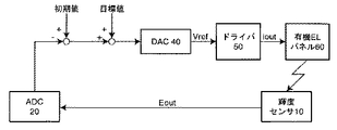
図1(a)に示すように、本実施例に係る有機EL表示装置は、フォトダイオードやCCD素子、C−MOS素子等で構成される輝度センサ10、ADC(アナログ−デジタル変換回路)20、有機ELパネル制御回路30、DAC(デジタル−アナログ変換器)40、及びデジタルデータに対応するデータ電流を生成する電流生成回路を含むドライバ50、及び有機ELパネル60で構成される。有機ELパネル制御回路30は、図1(b)に示すように、比較器30a、輝度テーブル30b、出力電圧テーブル30c、及びセレクタ30dで構成される。
【0021】
なお、輝度センサ10には、有機ELパネル60の点灯光以外の外光を検出しないよう、遮光されているか否かを判断する手段が設けられている。この遮光部については後述する実用例で説明する。また、有機ELパネル制御回路30は、各機能を実現する回路によりハードウエア構成する、あるいはマイコンを利用してソフトウエアにより機能を実現することができる。
なお、上述のように有機ELパネル60は、R(赤)、G(緑)、及びB(青)のそれぞれに対応した発光色を示す発光層を備えた複数の有機EL素子により構成してもよいし、共通の白色光源から発せられた光をR(赤)、G(緑)、及びB(青)に変換する色変換層をR(赤)、G(緑)、及びB(青)に対応して設けた複数の有機EL素子により構成することもできる。
【0022】
先ず、全体的な動作を説明すると、有機ELパネル60から発せられる光を輝度センサ10で検出し、検出結果として電圧EoutをADC20へ出力する。これをADC20はデジタル信号に変換して有機ELパネル制御回路30へ出力する。このデジタル信号が入力された比較器30aは、不揮発メモリ等に記憶された所定の輝度テーブル30bを参照し、検出された輝度が所定の輝度となっているか否か比較する。与えたデジタルデータhに応じて輝度テーブル30bの、検出結果Eoutと比較すべき輝度データを選択するようにしてもよい。
この比較結果をセレクタ30dへ出力する。この比較結果が入力されたセレクタ30dは、後に詳述するように、出力電圧テーブル30cから比較結果に基づき、適切な基準電圧Vrefが出力されるよう、指令値をDAC40へ出力する。この指令値に応じてDAC40は、後に詳述するように、補正した基準電圧Vrefをドライバ50に含まれるDACに出力する。この基準電圧Vrefはドライバ50に含まれるDACにおいてデジタルデータhをアナログ値に変換する際の基準電圧となる。このようにして、検出結果に基づいて有機ELパネル60へ供給するアナログデータが補正される。
【0023】
次に輝度補正の具体的な手法を説明する。調整シーケンスを表す図2のフローチャートに示すように、正確な輝度を測定するために遮光状態にあるか否かを確認し(S10)、遮光されている場合には調整(図中、キャリブレーション)を開始する(S10:YES→S20)。次に、前述した図1(b)の出力電圧テーブル30bを参照し、R(Red、赤)、G(Green、緑)、B(Blue、青)の各色毎に基準電圧Vrefを決定していく(S30乃至S80)。
なお、有機ELパネル60が共通の白色光源から発せられた光をR(赤)、G(緑)、及びB(青)に変換する色変換層をR(赤)、G(緑)、及びB(青)に対応して設けた複数の有機EL素子により構成されている場合は、当該共通の白色光源の輝度を検出するようにしてもよいし、R(赤)、G(緑)、及びB(青)のうち、少なくともどれか一色の輝度を検出するようにしてもよい。
【0024】
=====第二実施例=====
本実施例では、第一実施例のような出力電圧テーブルを用いることなく、輝度を測定しつつ、基準電圧Vrefを補正して目標輝度になるまで調整する。したがって、本実施例の全体構成としては、図1(a)の通りであるが、有機ELパネル制御回路30としては、図1(b)の構成でなく、図3に示す調整シーケンスを実現するプログラマブルマイコン等で構成する。この点、第一実施例に比べて回路規模を小さくできる。この点以外は、前述した第一実施例と共通するため、相違点を中心に説明する。
【0025】
具体的には、図3に示すように、遮光状態にあるか否かを確認し(S10)、遮光されている場合には調整(図中、キャリブレーション)を開始する(S20)。次に、R(Red、赤)、G(Green、緑)、B(Blue、青)の各色毎に基準電圧Vrefを順次決定していく(S10乃至S120)。この際、図6の画像データ値に対する輝度センサの出力電圧Eoutの特性グラフに示すように、両者の理想的な関係は、各色毎に目標値(EGtgt、EBtgt、ERtgt)を中心として目標調整範囲として定められている。この理想的な対応関係となるよう、各色毎に適宜な調整ステップ電圧(Rstep、Gstep、Bstep)を設けて各色毎の基準電圧VrefR、VrefG、VrefBを補正する。
【0026】
先ず、赤色(Red)の輝度補正を例に取り説明すると、図3に示すように、輝度センサの出力電圧ER(Eout)が図4の目標調整範囲内であれば(S50:YES)、他の色の輝度補正行い、そうでなければ(S50:NO)、基準電圧VrefRの調整を行う(S60)。その目標調整範囲とは、輝度センサの出力電圧ERがその目標値ERtgtの0.9倍乃至1.1倍の範囲である。この範囲を下回った場合には、基準電圧VrefRに調整ステップ電圧Rstepを加算して、基準電圧Vrefを上げることで低下した輝度を目標値へ近づけるように制御する。反対に、この範囲を越えた場合には、基準電圧VrefRに調整ステップ電圧Rstepを減算して、基準電圧Vrefを下げることで高くなり過ぎた輝度を目標値へ近づけるように制御する。以後、図3に示すように、Green及びBlueの各色についてでも、同様の制御を行う(S70乃至S120)。
【0027】
上記の一連のプロセスは、例えば、図5のように表わすこともできる。すなわち、有機ELパネルの輝度の検出結果EoutをADC20でデジタル値の変換し、初期値(例えば、出荷時の検出結果Eoutのデジタルデータ)と比較し、比較結果に応じて目標値となるようにデジタルデータを補正し、この補正されたデジタルデータをDAC40においてアナログ値に変換し、このアナログ値をドライバ50に含まれるDACの基準電圧Vrefとして設定する。
上記の一連のプロセスを行う期間を適宜設定すれば、連続して使用している間にダイナミックに輝度補正を行うことができる。
【0028】
上述の例では、輝度の検出結果に基づいてドライバ50に含まれるDACの基準電圧Vrefを調整しているが、これ以外に、駆動電圧やデータそのものを検出結果に応じて調整あるいは加工することも可能である。
例えば、図6に示すように検出結果EoutをADC20にてデジタル信号に変換して有機ELパネル制御回路内の比較器30aに入力し、比較器30aにて、不揮発メモリ等に記憶された所定の輝度テーブル30bを参照し、補正前の輝度に対して検出した輝度が所望の適正値となっているかどうかを比較する。この比較結果をセレクタ30dへ出力する。
なお、検出する際には予め設定した所定のデジタル信号が入力された際の輝度を検出し、その検出結果に対応するデータ(すなわち初期データ)を輝度テーブル30bに格納し、この初期データと比較することが好ましい。
この比較結果が入力されたセレクタ30dは、駆動電圧テーブル30eのデータから適切なデータを選択し、電源回路70に含まれるDACに出力する。このDACの出力が有機ELパネルに供給する駆動電圧Voelを決定する。
【0029】
また、図7に示すようにデジタルデータそのものを検出結果Eoutに応じて加工するようにしてもよい。この場合、検出結果EoutをADC20にてデジタル信号に変換して有機ELパネル制御回路内の比較器30aに入力し、比較器30aにて、不揮発メモリ等に記憶された所定の輝度テーブル30bを参照し、補正前の輝度が所望の輝度となっているか否か比較する。この比較結果をセレクタ30dへ出力し、この出力に基づいて出力データテーブルの中から適切なデータを選択し、データ補正回路80で行われる基準値を設定する。データ補正回路80で補正されたデジタルデータmがドライバ50に含まれるDACに入力された後、アナログ変換され、アナログデータioutが有機ELパネルに供給されることとなる。
図6及び図7に示した例は、図5に示したようなダイナミックな輝度補正にも適用可能である。
なお、有機EL素子の発光効率は環境温度に依存することもあるので、そのような場合、輝度を検出する代わりに温度を測定し、上述と同様な方法で、有機ELパネルのフィードバックすることも可能である。
【0030】
=====本発明の電気光学装置の搭載例=====
前述した有機EL表示装置を、折り畳み式であって携帯型の電話機やPDAなどの情報端末に適用した事例を説明する。折り畳み式携帯電話100の斜視図を図8に示す。同図に示す携帯電話100はヒンジメカニズム(ヒンジ部)110を利用して二つ折りタイプを実現しており、折り畳まずに開いた状態を示している。
【0031】
輝度センサ120の配置としては、折り畳んだ際に外部から光が入射しない遮蔽構造となるように、有機ELパネル130と対向して設けられ、なおかつ、その対向部分においてその中央に位置づけられる。また、この輝度センサ120は、デジタルカメラ内蔵型であればその光センサを兼用できる。
【0032】
また、輝度センサ120で有機ELパネル130の発光輝度の正確な測定を確保すべく、図9の側面図に示すように、携帯電話が折り畳まれてあるか否かを検出する部として遮光検出センサ140(輝度検出可能判定部)をヒンジ部110に設ける。同図に示すように、遮光検出センサ140の一例としては板ばね式のものを用い、有機ELパネル130側に突起140aを設けると共に、輝度センサ120側に板ばね140bを設ける。この構成により、輝度調整をすべく携帯電話100を折り畳んだ際に板バネ140bが突起140aの当接によって導通信号を出力する。このことで、上述の実施例のシーケンスにおける遮光状態の有無確認を実施することができる。この遮光検出センサ140の等価回路を示すと、例えば図10のようになる。
【0033】
また、遮光状態を検出するにあたり、前述したような遮光検出部を新たに設けることなく、非表示状態における輝度センサの出力が所定の閾値以下であれば遮光状態であると判断するようにしてもよい。この場合、遮光検出センサを新たに設けなくて済むため、部品手数を減らせて全体として簡易な構成で済ませることができる。
【0034】
さらに、輝度センサを折り畳まずに開いた状態では、経時劣化による輝度補償の目的だけではなく、外光の影響を相殺すべく、有機ELパネルの輝度調整をするための外光センサとしても用いることができる。
【0035】
なお、本発明にあっては、画素の色として、R、G、B(赤、緑、青)の三色だけに限らず、他の色でもよい。
【0036】
=====他の実用例=====
つぎに、上述した電子装置の一例として有機EL表示装置を具体的な電子機器に用いた例のいくつかについて説明する。まず、この実施形態に係る有機EL表示体をモバイル型のパーソナルコンピュータに適用した例について説明する。図11は、このモバイル型のパーソナルコンピュータの構成を示す斜視図である。同図において、パーソナルコンピュータ1100は、キーボード1102を備えた本体部1104と、表示ユニット1106とにより構成され、この表示ユニット1106が前述の有機EL表示装置を備えている。
【0037】
また、図12は前述の有機EL表示装置を、そのファインダに適用したディジタルスチルカメラの構成を示す斜視図である。なお、この図には外部機器との接続についても簡易的に示している。ここで通常のカメラは、被写体の光像によりフィルムを感光するのに対し、ディジタルスチルカメラ1300は、被写体の光像をCCD(Charge Coupled Device)などの撮像素子により光電変換して撮像信号を生成する。ディジタルスチルカメラ1300におけるケース1302の背面には、前述の有機EL表示装置が設けられ、CCDによる撮像信号に基づいて表示を行う構成になっており、有機EL表示装置は被写体を表示するファインダとして機能する。また、ケース1302の観察側(図においては裏面側)には、光学レンズやCCDなどを含んだ受光ユニット1304が設けられている。
【0038】
撮影者が有機EL表示装置に表示された被写体像を確認しシャッタボタン1306を押下すると、その時点におけるCCDの撮像信号が、回路基板1308のメモリに転送・格納される。また、このディジタルスチルカメラ1300にあっては、ケース1302の側面に、ビデオ信号出力端子1312と、データ通信用の入出力端子1314とが設けられている。そして、図に示されるように、前者のビデオ信号出力端子1312にはテレビモニタ1430が、また、後者のデータ通信用の入出力端子1314にはパーソナルコンピュータ1430が、それぞれ必要に応じて接続される。さらに、所定の操作により回路基板1308のメモリに格納された撮像信号が、テレビモニタ1430や、パーソナルコンピュータ1440に出力される構成になっている。
【0039】
なお、本発明の有機EL表示装置が適用される電子機器としては、図11のパーソナルコンピュータや、図12のディジタルスチルカメラの他にも、テレビや、ビューファインダ型、モニタ直視型のビデオテープレコーダ、カーナビゲーション装置、ページャ、電子手帳、電卓、ワードプロセッサ、ワークステーション、テレビ電話、POS端末、タッチパネルを備えた機器、スマートロボット、調光付き照明機器、電子書籍などが挙げられる。そして、これらの各種電子機器の表示部として、前述した有機EL表示装置が適用可能なのは言うまでもない。
【0040】
電気光学素子に供給する駆動電流の量を調整することにより、輝度の変化を補償することができる。具体的には、輝度を一定に保つことができ、画像データの色再現性の劣化が極めて抑えることができる。
【図面の簡単な説明】
【図1】本発明に係る有機EL表示装置を示し、(a)は全体の制御ブロック図であり、(b)は有機EL制御回路30の制御ブロック図である。
【図2】本発明に係る有機EL表示装置の輝度補正のシーケンス制御を示すフローチャートである。
【図3】本発明に係る有機EL表示装置の輝度補正のシーケンス制御を示すフローチャートである。
【図4】本発明に係る有機EL表示装置における、画像データ値に対する輝度センサの出力電圧Eoutの特性グラフである。
【図5】本発明に係る有機EL表示装置のダイナミックな輝度補正に関するブロック図である。
【図6】本発明に係る有機EL表示装置を示し、(a)は全体の制御ブロック図であり、(b)は有機EL制御回路30の制御ブロック図である。
【図7】本発明に係る有機EL表示装置を示し、(a)は全体の制御ブロック図であり、(b)は有機EL制御回路30の制御ブロック図である。
【図8】本発明の実施例に係る有機EL表示装置の一実用例である折り畳み式携帯電話100の斜視図である。
【図9】図8で示した携帯電話の側面図である。
【図10】本発明の一実施形態に係る有機EL表示装置における遮光検出センサ140の等価回路図である。
【図11】本発明の一実施例による電気光学装置を、モバイル型のパーソナルコンピュータに適用した場合の一例を示す図である。
【図12】本発明の一実施例による電気光学装置を、そのファインダに適用したディジタルスチルカメラの斜視図である。
【符号の説明】
10 輝度センサ
20 アナログ−デジタル変換回路
30 有機ELパネル制御回路
40 デジタル−アナログ変換器
50 ドライバ
60 有機ELパネル
30a 比較器30a
30b 輝度テーブル
30c 出力電圧テーブル
30d セレクタ
100 携帯電話
110 ヒンジメカニズム(ヒンジ部)
120 輝度センサ
130 有機ELパネル
1100 パーソナルコンピュータ
1102 キーボード
1104 本体部
1106 表示ユニット
1300 ディジタルスチルカメラ
1302 ケース
1304 受光ユニット
1306 シャッタボタン
1308 回路基板
1312 ビデオ信号出力端子
1314 データ通信用の入出力端子
1430 テレビモニタ
1440 パーソナルコンピュータ[0001]
TECHNICAL FIELD OF THE INVENTION
The present invention relates to an electro-optical device, a driving method thereof, and an electronic apparatus.
[0002]
[Prior art]
For example, in an organic EL (electroluminescence) display device, there is a circumstance in which the lighting luminance of the organic EL element constituting the organic EL device deteriorates with time much faster than that of an inorganic EL display device. That is, when the lighting time is accumulated, the luminance is significantly reduced. More specifically, the life of the inorganic EL display device exceeds 100,000 hours, and the luminance hardly decreases. On the other hand, in the case of the organic EL display device, when it is lit at a luminance of, for example, 300 cd / m 2 , the limit is about 10,000 hours.
Therefore, as described in Patent Literature 1 and Patent Literature 2, measures have been taken by improving the manufacturing method.
[Patent Document 1] JP-A-11-154596 [Patent Document 2] JP-A-11-214257
[Problems to be solved by the invention]
However, in reality, it is difficult to completely prevent the occurrence of luminance reduction by the approach of improving the manufacturing method. The present invention has been made to solve such a problem, and an object of the present invention is to provide a technique for compensating a temporal change in luminance by a circuit technical approach.
[0005]
[Means for Solving the Problems]
In the first electro-optical device according to the present invention, the plurality of scanning lines, the plurality of signal lines, and the electro-optical devices arranged corresponding to the intersections of the respective scanning lines and the respective signal lines. An electro-optical device that operates according to the amount of drive current supplied to the electro-optical element, and a luminance detecting unit that detects the luminance of the electro-optical element, and the luminance of the electro-optical element. A driving current amount adjusting unit configured to adjust the driving current amount based on the luminance detection result obtained by the luminance detecting unit for correction.
The drive current amount is defined by a value of the drive current and a length of a period for supplying the drive current to the electro-optical device.
[0006]
A second electro-optical device according to the present invention includes a plurality of scanning lines, a plurality of signal lines, and an electro-optical element provided corresponding to an intersection of each of the scanning lines and each of the signal lines. An electro-optical device comprising: a DA converter that converts digital data into analog data; a driver that supplies analog data to the electro-optical element; a luminance detecting unit that detects luminance of the electro-optical element; A reference voltage adjusting unit that adjusts a reference voltage of the DA converter based on the luminance detection result obtained by the unit.
A third electro-optical device according to the present invention includes a plurality of scanning lines, a plurality of signal lines, and an electro-optical element provided corresponding to an intersection of each of the scanning lines and each of the signal lines. An electro-optical device comprising: a driver for supplying luminance data to the electro-optical element; a control circuit for supplying digital data serving as a basis of the luminance data to the driver; and detecting a luminance of the electro-optical element A luminance detection unit; and a data correction circuit that corrects the digital data based on a luminance detection result obtained by the luminance detection unit.
[0007]
Ordinary electro-optical devices such as liquid crystal devices and electroluminescent devices often include three types of electro-optical elements of R (red), G (green), and B (blue). In such an electro-optical device, the electro-optical element includes three types of electro-optical elements of R (red), G (green), and B (blue), and the luminance detecting unit includes the three types of electro-optical elements. The luminance may be detected for each type of element, and the driving current amount adjustment unit may adjust the driving current amount based on the detected luminance for each type.
The three types of electro-optical elements are configured such that light emitted from a light source common to the three types of electro-optical elements passes through a color conversion unit provided for each of the three types of electro-optical elements, In the case where the light is emitted in R (red), G (green), and B (blue), the luminance detecting section may detect the luminance of the common light source as the luminance of the electro-optical element, or Light passing through at least one of the three types of electro-optical elements may be detected as the luminance of the electro-optical element.
[0008]
Furthermore, it is preferable that the apparatus further includes a luminance detection possible determination unit that determines whether or not the luminance detection by the luminance detection unit is possible.
[0009]
Furthermore, it may be determined whether or not the brightness detection unit can detect the brightness based on the brightness of the electro-optical element detected by the brightness detection unit.
[0010]
Further, in the electronic apparatus according to the present invention, the above-described electro-optical device is mounted.
[0011]
In the first driving method of the electro-optical device according to the present invention, a plurality of scanning lines, a plurality of signal lines, and a plurality of signal lines are arranged corresponding to respective intersections of the respective scanning lines and the respective signal lines. A driving method for an electro-optical device comprising an electro-optical element provided, and operating according to an amount of driving current supplied to the electro-optical element, wherein a first step of detecting a luminance of the electro-optical element; And a second step of adjusting the drive current amount based on the detection result obtained in the first step.
[0012]
According to a second method of driving an electro-optical device of the present invention, the electro-optical device includes a plurality of scanning lines, a plurality of signal lines, and an electro-optical device disposed corresponding to an intersection of each of the scanning lines and each of the signal lines. A method for driving an electro-optical device, comprising: a device and a DA converter that converts digital data into analog data; and a driver that supplies analog data to the electro-optical device. And a second step of setting a reference voltage of the DA converter based on a result of the detection result obtained in the first step.
According to a third driving method of the electro-optical device of the present invention, the electro-optical device includes a plurality of scanning lines, a plurality of signal lines, and an electro-optical device arranged corresponding to an intersection of each of the scanning lines and each of the signal lines. A driving method for an electro-optical device, comprising: an element; and supplying luminance data to the electro-optical element via a driver, wherein a first step of detecting the luminance of the electro-optical element and a first step of detecting the luminance of the electro-optical element. And a second step of correcting the digital data based on the obtained detection result.
In the first step of the method for driving an electro-optical device, it is preferable that the luminance is detected for each of three colors of R, G, and B (red, green, and blue).
[0013]
Further, prior to the first step, it may be determined in advance whether or not the luminance can be detected.
[0014]
Furthermore, based on the detected brightness of the electro-optical element, it may be determined whether or not the brightness detection unit can detect the brightness.
[0015]
In the present invention, the colors of the pixels are not limited to the three colors of R, G, and B (red, green, and blue), and may be other colors.
[0016]
Other features of the present invention will become apparent from the accompanying drawings and the following description.
[0017]
BEST MODE FOR CARRYING OUT THE INVENTION
An embodiment of the present invention will be described. In the present embodiment, a display device (hereinafter, referred to as an organic EL display device) using an organic electroluminescence device (hereinafter, referred to as an organic EL device) and a driving method thereof will be described as an example of the electro-optical device.
[0018]
First, an organic EL display device will be briefly described. As is well known, an organic EL panel constituting an organic EL display device is formed by arranging unit pixels including organic EL elements in a matrix. As the circuit configuration and operation of the unit pixel, for example, as described in a book titled “Electronic Display” (written by Shoichi Matsumoto, published by Ohm Co., Ltd., issued on June 20, 1996) (mainly, 137), a driving current is supplied to each unit pixel, and a predetermined voltage is written to an analog memory composed of two transistors and a capacitor, thereby controlling lighting (lighting) of the organic EL element.
[0019]
In the embodiment according to the present invention, the luminance of the display panel of the organic EL display device is detected by the luminance sensor, and the luminance is corrected based on the detection result.
[0020]
===== First Embodiment =====
As shown in FIG. 1A, the organic EL display device according to the present embodiment includes a
[0021]
Note that the
Note that, as described above, the
[0022]
First, the overall operation will be described. Light emitted from the
The comparison result is output to the selector 30d. The selector 30d to which the comparison result is input outputs a command value to the
[0023]
Next, a specific method of luminance correction will be described. As shown in the flowchart of FIG. 2 showing the adjustment sequence, it is checked whether or not the light is shielded in order to measure an accurate luminance (S10). If the light is shielded, adjustment is performed (calibration in the figure). Is started (S10: YES → S20). Next, the reference voltage Vref is determined for each of R (Red, Red), G (Green, Green), and B (Blue, Blue) by referring to the output voltage table 30b of FIG. (S30 to S80).
The
[0024]
===== Second Embodiment =====
In this embodiment, the reference voltage Vref is corrected and adjusted until the target brightness is obtained while measuring the brightness without using the output voltage table as in the first embodiment. Therefore, the overall configuration of this embodiment is as shown in FIG. 1A, but the organic EL
[0025]
Specifically, as shown in FIG. 3, it is checked whether or not the light is shielded (S10). If the light is shielded, adjustment (calibration in the figure) is started (S20). Next, the reference voltage Vref is sequentially determined for each of R (Red, Red), G (Green, Green), and B (Blue, Blue) colors (S10 to S120). At this time, as shown in the characteristic graph of the output voltage Eout of the luminance sensor with respect to the image data value in FIG. 6, the ideal relationship between the two is that the target adjustment range is centered on the target value (EGtgt, EBtgt, ERtgt) for each color. It is defined as. Appropriate adjustment step voltages (Rstep, Gstep, Bstep) are provided for each color so as to provide this ideal correspondence, and the reference voltages VrefR, VrefG, VrefB for each color are corrected.
[0026]
First, a description will be given of the luminance correction of red (Red) as an example. As shown in FIG. 3, if the output voltage ER (Eout) of the luminance sensor is within the target adjustment range of FIG. 4 (S50: YES), The luminance of the color is corrected, otherwise (S50: NO), the reference voltage VrefR is adjusted (S60). The target adjustment range is a range in which the output voltage ER of the luminance sensor is 0.9 to 1.1 times the target value ERtgt. When the value falls below this range, the adjustment step voltage Rstep is added to the reference voltage VrefR, and the reference voltage Vref is increased to control the lowered luminance to approach the target value. Conversely, when the value exceeds this range, the adjustment step voltage Rstep is subtracted from the reference voltage VrefR, and the control is performed so that the excessively high luminance approaches the target value by lowering the reference voltage Vref. Thereafter, as shown in FIG. 3, the same control is performed for each of the green and blue colors (S70 to S120).
[0027]
The above series of processes can be represented, for example, as shown in FIG. That is, the detection result Eout of the luminance of the organic EL panel is converted into a digital value by the
By appropriately setting the period during which the above-described series of processes are performed, it is possible to dynamically perform luminance correction during continuous use.
[0028]
In the above example, the reference voltage Vref of the DAC included in the
For example, as shown in FIG. 6, the detection result Eout is converted into a digital signal by the
At the time of detection, the luminance when a predetermined digital signal set in advance is input is detected, data corresponding to the detection result (that is, initial data) is stored in the luminance table 30b, and compared with the initial data. Is preferred.
The selector 30d to which the comparison result is input selects appropriate data from the data of the drive voltage table 30e and outputs the selected data to the DAC included in the
[0029]
Further, as shown in FIG. 7, the digital data itself may be processed according to the detection result Eout. In this case, the detection result Eout is converted into a digital signal by the
The examples shown in FIGS. 6 and 7 are also applicable to the dynamic luminance correction as shown in FIG.
In addition, since the luminous efficiency of the organic EL element may depend on the environmental temperature, in such a case, the temperature is measured instead of detecting the luminance, and the feedback of the organic EL panel may be performed in the same manner as described above. It is possible.
[0030]
===== Example of mounting the electro-optical device of the present invention =====
An example in which the above-described organic EL display device is applied to a foldable information terminal such as a portable telephone or a PDA will be described. FIG. 8 shows a perspective view of the foldable
[0031]
The
[0032]
In addition, as shown in the side view of FIG. 9, a light-shielding detection sensor is used as a unit for detecting whether or not the mobile phone is folded, in order to ensure accurate measurement of the emission luminance of the
[0033]
Further, in detecting the light-shielded state, the light-shielded state may be determined if the output of the luminance sensor in the non-display state is equal to or less than a predetermined threshold value without newly providing the light-shielded detection unit as described above. Good. In this case, since it is not necessary to newly provide a light-shielding detection sensor, the number of parts can be reduced, and the whole configuration can be simplified.
[0034]
Furthermore, when the luminance sensor is opened without being folded, it is used not only for the purpose of luminance compensation due to aging deterioration but also as an external light sensor for adjusting the luminance of the organic EL panel in order to offset the influence of external light. Can be.
[0035]
In the present invention, the colors of the pixels are not limited to the three colors of R, G, and B (red, green, and blue), and may be other colors.
[0036]
===== Other practical examples =====
Next, as examples of the above-described electronic devices, some examples in which an organic EL display device is used in specific electronic devices will be described. First, an example in which the organic EL display according to this embodiment is applied to a mobile personal computer will be described. FIG. 11 is a perspective view showing the configuration of the mobile personal computer. In the figure, a
[0037]
FIG. 12 is a perspective view showing a configuration of a digital still camera in which the above-described organic EL display device is applied to a finder thereof. In this figure, connection with an external device is simply shown. Here, an ordinary camera exposes a film with an optical image of an object, whereas a
[0038]
When the photographer confirms the subject image displayed on the organic EL display device and presses the
[0039]
As the electronic apparatus to which the organic EL display device of the present invention is applied, in addition to the personal computer shown in FIG. 11 and the digital still camera shown in FIG. 12, a television, a viewfinder type, and a monitor direct-view type video tape recorder can be used. , A car navigation device, a pager, an electronic organizer, a calculator, a word processor, a workstation, a videophone, a POS terminal, a device equipped with a touch panel, a smart robot, a lighting device with dimming, and an electronic book. Needless to say, the above-described organic EL display device can be applied as a display unit of these various electronic devices.
[0040]
By adjusting the amount of drive current supplied to the electro-optical element, a change in luminance can be compensated. Specifically, the luminance can be kept constant, and the deterioration of the color reproducibility of the image data can be extremely suppressed.
[Brief description of the drawings]
1A and 1B show an organic EL display device according to the present invention, wherein FIG. 1A is an overall control block diagram, and FIG. 1B is a control block diagram of an organic
FIG. 2 is a flowchart illustrating sequence control of luminance correction of the organic EL display device according to the present invention.
FIG. 3 is a flowchart showing sequence control of luminance correction of the organic EL display device according to the present invention.
FIG. 4 is a characteristic graph of an output voltage Eout of a luminance sensor with respect to an image data value in the organic EL display device according to the present invention.
FIG. 5 is a block diagram relating to dynamic luminance correction of the organic EL display device according to the present invention.
6A and 6B show an organic EL display device according to the present invention, wherein FIG. 6A is an overall control block diagram, and FIG. 6B is a control block diagram of an organic
7A and 7B show an organic EL display device according to the present invention, in which FIG. 7A is an overall control block diagram, and FIG. 7B is a control block diagram of an organic
FIG. 8 is a perspective view of a foldable
9 is a side view of the mobile phone shown in FIG.
FIG. 10 is an equivalent circuit diagram of a light
FIG. 11 is a diagram showing an example in which the electro-optical device according to one embodiment of the present invention is applied to a mobile personal computer.
FIG. 12 is a perspective view of a digital still camera in which the electro-optical device according to one embodiment of the present invention is applied to a finder thereof.
[Explanation of symbols]
30b brightness table 30c output voltage
120
Claims (15)
前記電気光学素子の輝度を検出する輝度検出部と、
前記輝度検出部で得られた輝度検出結果に基づき前記駆動電流量を調整する駆動電流量調整部と、
を備えることを特徴とする電気光学装置。A plurality of scanning lines, a plurality of signal lines, and an electro-optical element disposed corresponding to an intersection of each of the scanning lines and each of the signal lines, and a driving current supplied to the electro-optical element. An electro-optical device that operates according to the amount of
A brightness detection unit that detects the brightness of the electro-optical element,
A drive current amount adjustment unit that adjusts the drive current amount based on the luminance detection result obtained by the luminance detection unit,
An electro-optical device comprising:
デジタルデータをアナログ変換するDAコンバータを含み、前記電気光学素子にアナログデータを供給するドライバと、
前記電気光学素子の輝度を検出する輝度検出部と、
前記輝度検出部で得られた輝度検出結果に基づき前記DAコンバータの基準電圧を調整する基準電圧調整部と、
を備えることを特徴とする電気光学装置。An electro-optical device including a plurality of scanning lines, a plurality of signal lines, and an electro-optical element arranged corresponding to an intersection of each of the scanning lines and each of the signal lines,
A driver that includes a DA converter that converts digital data to analog, and supplies analog data to the electro-optical element,
A brightness detection unit that detects the brightness of the electro-optical element,
A reference voltage adjustment unit that adjusts a reference voltage of the DA converter based on the luminance detection result obtained by the luminance detection unit;
An electro-optical device comprising:
前記電気光学素子に輝度データを供給するドライバと、
前記ドライバに前記輝度データの基となるデジタルデータを供給する制御回路と、
前記電気光学素子の輝度を検出する輝度検出部と、
前記輝度検出部で得られた輝度検出結果に基づき前記デジタルデータを補正するデータ補正回路と、
を備えることを特徴とする電気光学装置。An electro-optical device including a plurality of scanning lines, a plurality of signal lines, and an electro-optical element arranged corresponding to an intersection of each of the scanning lines and each of the signal lines,
A driver for supplying luminance data to the electro-optical element,
A control circuit for supplying the driver with digital data based on the luminance data,
A brightness detection unit that detects the brightness of the electro-optical element,
A data correction circuit that corrects the digital data based on the luminance detection result obtained by the luminance detection unit,
An electro-optical device comprising:
前記電気光学素子は、R(赤)、G(緑)、B(青)の3種類の電気光学素子を含み、
前記輝度検出部は前記3種類の電気光学素子の種類毎に前記輝度を検出すること、
を特徴とする電気光学装置。The electro-optical device according to claim 1,
The electro-optical element includes three types of electro-optical elements of R (red), G (green), and B (blue),
The brightness detection unit detects the brightness for each of the three types of electro-optical elements,
An electro-optical device comprising:
前記電気光学素子は、R(赤)、G(緑)、B(青)の3種類の電気光学素子を含み、
前記3種類の電気光学素子は、前記3種類の電気光学素子に共通の光源が発した光が前記3種類の電気光学素子の各々に対応して設けられた色変換部を通過することにより、R(赤)、G(緑)、B(青)に発色し、
前記輝度検出部は、前記共通の光源の輝度を前記電気光学素子の輝度として検出すること、
を特徴とする電気光学装置。The electro-optical device according to claim 1,
The electro-optical element includes three types of electro-optical elements of R (red), G (green), and B (blue),
The three types of electro-optical elements are configured such that light emitted from a light source common to the three types of electro-optical elements passes through a color conversion unit provided for each of the three types of electro-optical elements, R (red), G (green), B (blue)
The brightness detection unit detects the brightness of the common light source as the brightness of the electro-optical element,
An electro-optical device comprising:
前記電気光学素子は、R(赤)、G(緑)、B(青)の3種類の電気光学素子を含み、
前記3種類の電気光学素子は、前記3種類の電気光学素子に共通の光源が発した光が前記3種類の電気光学素子の各々に対応して設けられた色変換部を通過することにより、R(赤)、G(緑)、B(青)に発色し、
前記輝度検出部は、前記3種類の電気光学素子の少なくともいずれかの前記色変換部を通過する光を前記電気光学素子の輝度として検出すること、
を特徴とする電気光学装置。The electro-optical device according to claim 1,
The electro-optical element includes three types of electro-optical elements of R (red), G (green), and B (blue),
The three types of electro-optical elements are configured such that light emitted from a light source common to the three types of electro-optical elements passes through a color conversion unit provided for each of the three types of electro-optical elements, R (red), G (green), B (blue)
The brightness detection unit detects light passing through the color conversion unit of at least one of the three types of electro-optic elements as brightness of the electro-optic element,
An electro-optical device comprising:
前記輝度検出部による前記輝度検出が可能な状態であるか否かを判定する輝度検出可能判定部を更に備えることを特徴とする電気光学装置。The electro-optical device according to any one of claims 1 to 6,
An electro-optical device, further comprising: a luminance detection possible determination unit that determines whether or not the luminance detection by the luminance detection unit is possible.
前記輝度検出部によって検出された前記電気光学素子の前記輝度に基づき、前記輝度検出部による前記輝度検出が可能な状態であるか否かを判定することを特徴とする電気光学装置。The electro-optical device according to claim 1, wherein
An electro-optical device, comprising: determining whether or not the luminance detection unit can detect the luminance based on the luminance of the electro-optical element detected by the luminance detection unit.
前記電気光学素子の輝度を検出する第1のステップと、
前記前記輝度の検出結果に基づき前記駆動電流量を調整する第2のステップと、
を備えることを特徴とする電気光学装置の駆動方法。A method for driving an electro-optical device, comprising: a plurality of scanning lines; a plurality of signal lines; and an electro-optical element disposed corresponding to an intersection of each of the scanning lines and each of the signal lines. ,
A first step of detecting the brightness of the electro-optical element;
A second step of adjusting the drive current amount based on the luminance detection result;
A method for driving an electro-optical device, comprising:
前記電気光学素子の輝度を検出する第1のステップと、
前記第1のステップで得られた検出結果に基づき前記DAコンバータの基準電圧を設定する第2のステップと、
を備えることを特徴とする電気光学装置の駆動方法。A plurality of scanning lines, a plurality of signal lines, an electro-optical element disposed corresponding to the intersection of each of the scanning lines and each of the signal lines, and a DA converter for converting digital data to analog, A driver for supplying analog data to the electro-optical element, and a driving method of the electro-optical device, comprising:
A first step of detecting the brightness of the electro-optical element;
A second step of setting a reference voltage of the DA converter based on the detection result obtained in the first step;
A method for driving an electro-optical device, comprising:
前記電気光学素子の輝度を検出する第1のステップと、
前記第1のステップで得られた検出結果に基づき前記デジタルデータを補正する第2のステップと、
を備えることを特徴とする電気光学装置の駆動方法。A plurality of scanning lines, a plurality of signal lines, and an electro-optical element disposed corresponding to an intersection of each of the scanning lines and each of the signal lines, and the electro-optical element is connected to the electro-optical element via a driver. A method for driving an electro-optical device that supplies luminance data,
A first step of detecting the brightness of the electro-optical element;
A second step of correcting the digital data based on the detection result obtained in the first step;
A method for driving an electro-optical device, comprising:
前記第1のステップにおいて、R、G、B(赤、緑、青)の三色別に輝度を検出することを特徴とする電気光学装置の駆動方法。A method for driving an electro-optical device according to claim 11 or 12,
The method of driving an electro-optical device according to claim 1, wherein in the first step, luminance is detected for each of three colors of R, G, and B (red, green, and blue).
前記第1のステップに先立ち、
予め当該輝度検出が可能な状態であるか否かを判定することを特徴とする電気光学装置の駆動方法。The method for driving an electro-optical device according to claim 10,
Prior to the first step,
A method for driving an electro-optical device, comprising: determining in advance whether or not the luminance can be detected.
検出された前記電気光学素子の前記輝度に基づき、前記輝度検出部による前記輝度検出が可能な状態であるか否かを判定することを特徴とする電気光学装置の駆動方法。The method for driving an electro-optical device according to claim 10,
A method for driving an electro-optical device, comprising: determining whether or not the luminance can be detected by the luminance detection unit based on the detected luminance of the electro-optical element.
Priority Applications (5)
| Application Number | Priority Date | Filing Date | Title |
|---|---|---|---|
| TW092102633A TW200307901A (en) | 2002-02-01 | 2003-01-30 | Electro-optical device, driving method thereof and electronic apparatus |
| KR10-2003-0006390A KR20030066421A (en) | 2002-02-01 | 2003-01-30 | Electrooptical device, driving method of the same, and electronic appliances |
| JP2003022024A JP2004029714A (en) | 2002-02-01 | 2003-01-30 | Electrooptical device, its driving method, and electronic apparatus |
| US10/353,933 US7253813B2 (en) | 2002-02-01 | 2003-01-30 | Electro-optical device, driving method thereof, and electronic apparatus |
| CNB031042449A CN1231882C (en) | 2002-02-01 | 2003-02-08 | Electro-optical device, driving method thereof and electronic apparatus |
Applications Claiming Priority (2)
| Application Number | Priority Date | Filing Date | Title |
|---|---|---|---|
| JP2002026130 | 2002-02-01 | ||
| JP2003022024A JP2004029714A (en) | 2002-02-01 | 2003-01-30 | Electrooptical device, its driving method, and electronic apparatus |
Publications (2)
| Publication Number | Publication Date |
|---|---|
| JP2004029714A true JP2004029714A (en) | 2004-01-29 |
| JP2004029714A5 JP2004029714A5 (en) | 2005-09-22 |
Family
ID=27667486
Family Applications (1)
| Application Number | Title | Priority Date | Filing Date |
|---|---|---|---|
| JP2003022024A Pending JP2004029714A (en) | 2002-02-01 | 2003-01-30 | Electrooptical device, its driving method, and electronic apparatus |
Country Status (5)
| Country | Link |
|---|---|
| US (1) | US7253813B2 (en) |
| JP (1) | JP2004029714A (en) |
| KR (1) | KR20030066421A (en) |
| CN (1) | CN1231882C (en) |
| TW (1) | TW200307901A (en) |
Cited By (6)
| Publication number | Priority date | Publication date | Assignee | Title |
|---|---|---|---|---|
| JP2008257201A (en) * | 2007-04-06 | 2008-10-23 | Samsung Sdi Co Ltd | Organic light emitting diode display and method of driving the same |
| JP2009511973A (en) * | 2005-10-14 | 2009-03-19 | ケンブリッジ ディスプレイ テクノロジー リミテッド | Display monitoring system |
| US7728526B2 (en) | 2006-03-29 | 2010-06-01 | Samsung Mobile Display Co., Ltd. | Organic light emitting display device and driving method for the same |
| JP2011048037A (en) * | 2009-08-26 | 2011-03-10 | Hitachi Displays Ltd | Display device |
| JP2012042913A (en) * | 2010-08-20 | 2012-03-01 | Samsung Electro-Mechanics Co Ltd | Organic light emitting diode driver |
| WO2014057588A1 (en) * | 2012-10-12 | 2014-04-17 | Necディスプレイソリューションズ株式会社 | Brightness calibrator, program, and brightness calibration method |
Families Citing this family (17)
| Publication number | Priority date | Publication date | Assignee | Title |
|---|---|---|---|---|
| KR20050085039A (en) * | 2002-11-21 | 2005-08-29 | 코닌클리케 필립스 일렉트로닉스 엔.브이. | Method of improving the output uniformity of a display device |
| JP5021884B2 (en) * | 2003-08-06 | 2012-09-12 | 日本電気株式会社 | Display drive circuit and display device using the same |
| JP2005099713A (en) * | 2003-08-25 | 2005-04-14 | Seiko Epson Corp | Electro-optical device, driving method therefor, and electronic apparatus |
| KR100581866B1 (en) * | 2003-10-15 | 2006-05-22 | 삼성에스디아이 주식회사 | Method and apparatus for white balance adjustment, and display panel comprising the same |
| JP4198121B2 (en) * | 2004-03-18 | 2008-12-17 | 三洋電機株式会社 | Display device |
| TWI278824B (en) * | 2004-03-30 | 2007-04-11 | Au Optronics Corp | Method and apparatus for gamma correction and flat-panel display using the same |
| JP4413085B2 (en) * | 2004-06-14 | 2010-02-10 | セイコーエプソン株式会社 | Video display method and video display device |
| KR101060450B1 (en) | 2004-09-30 | 2011-08-29 | 엘지디스플레이 주식회사 | OLED display device |
| KR20070083352A (en) * | 2006-02-21 | 2007-08-24 | 삼성전자주식회사 | Display device and driving method thereof |
| KR100872352B1 (en) * | 2006-11-28 | 2008-12-09 | 한국과학기술원 | Data driving circuit and organic light emitting display comprising thereof |
| JP5317419B2 (en) * | 2007-03-07 | 2013-10-16 | 株式会社ジャパンディスプレイ | Organic EL display device |
| KR20100069505A (en) * | 2008-12-16 | 2010-06-24 | 삼성에스디아이 주식회사 | Display apparatus having touch screen function |
| CN104021773B (en) | 2014-05-30 | 2015-09-09 | 京东方科技集团股份有限公司 | A kind of luminance compensation method of display device, luminance compensating mechanism and display device |
| CN104021761B (en) | 2014-05-30 | 2016-03-09 | 京东方科技集团股份有限公司 | A kind of luminance compensation method of display device, device and display device |
| TWI574581B (en) * | 2015-07-03 | 2017-03-11 | 點晶科技股份有限公司 | Dot correction method and system for led display device |
| CN109616054B (en) * | 2019-02-27 | 2020-07-28 | Oppo广东移动通信有限公司 | Brightness compensation method, display and computer storage medium |
| CN110310588A (en) * | 2019-06-27 | 2019-10-08 | 昆山国显光电有限公司 | A kind of display device |
Family Cites Families (29)
| Publication number | Priority date | Publication date | Assignee | Title |
|---|---|---|---|---|
| JPS6033391A (en) | 1983-08-03 | 1985-02-20 | Showa Alum Corp | Surface processing method of aluminum material excellent in wear resistance and lubricating characteristics |
| JPH04233854A (en) | 1990-12-28 | 1992-08-21 | Sony Corp | Portable telephone set |
| JPH0774691A (en) | 1993-08-31 | 1995-03-17 | Sanyo Electric Co Ltd | Portable telephone set with folding mechanism |
| WO1998040871A1 (en) | 1997-03-12 | 1998-09-17 | Seiko Epson Corporation | Pixel circuit, display device and electronic equipment having current-driven light-emitting device |
| JPH10254410A (en) | 1997-03-12 | 1998-09-25 | Pioneer Electron Corp | Organic electroluminescent display device, and driving method therefor |
| US6069597A (en) | 1997-08-29 | 2000-05-30 | Candescent Technologies Corporation | Circuit and method for controlling the brightness of an FED device |
| US6411306B1 (en) * | 1997-11-14 | 2002-06-25 | Eastman Kodak Company | Automatic luminance and contrast adustment for display device |
| JPH11154596A (en) | 1997-11-21 | 1999-06-08 | Matsushita Electric Ind Co Ltd | Organic electroluminescent element |
| KR100508964B1 (en) | 1998-01-23 | 2005-11-11 | 엘지전자 주식회사 | Method of Applying Sustain Pulse to Plasma Display |
| JP3554778B2 (en) | 1998-01-23 | 2004-08-18 | 株式会社村田製作所 | Nonlinear dielectric element |
| CA2294438A1 (en) | 1998-04-30 | 1999-11-11 | Hisashi Aoki | Display device using ambient light and a lighting panel |
| JP2000322022A (en) | 1998-06-05 | 2000-11-24 | Canon Inc | Image forming device and image forming method |
| JP2000184013A (en) | 1998-12-17 | 2000-06-30 | Nec Corp | Portable telephone set with camera |
| JP2000270069A (en) | 1999-03-16 | 2000-09-29 | Canon Inc | Portable information terminal with digital camera |
| JP3719580B2 (en) | 1999-05-14 | 2005-11-24 | 日本電気株式会社 | Mobile phone device with camera |
| US6633301B1 (en) * | 1999-05-17 | 2003-10-14 | Displaytech, Inc. | RGB illuminator with calibration via single detector servo |
| JP3792950B2 (en) | 1999-07-15 | 2006-07-05 | セイコーインスツル株式会社 | Organic EL display device and driving method of organic EL element |
| IL131242A0 (en) | 1999-08-04 | 2001-01-28 | Given Imaging Ltd | A method for temperature sensing |
| JP2001075524A (en) | 1999-09-03 | 2001-03-23 | Rohm Co Ltd | Display device |
| JP2001092412A (en) | 1999-09-17 | 2001-04-06 | Pioneer Electronic Corp | Active matrix type display device |
| KR20010029073A (en) | 1999-09-29 | 2001-04-06 | 구자홍 | Apparatus for arbitrating brightness of plasma display panel |
| JP4145495B2 (en) | 2000-01-11 | 2008-09-03 | 株式会社半導体エネルギー研究所 | Display device, computer, video camera, digital camera, goggle type display, navigation system, sound playback device, game machine, portable information terminal, and image playback device |
| TW480727B (en) * | 2000-01-11 | 2002-03-21 | Semiconductor Energy Laboratro | Semiconductor display device |
| JP5008223B2 (en) | 2000-01-31 | 2012-08-22 | 株式会社半導体エネルギー研究所 | Active matrix display device |
| JP4501205B2 (en) | 2000-02-08 | 2010-07-14 | 日亜化学工業株式会社 | Correction system and correction method for image display device |
| US6414661B1 (en) * | 2000-02-22 | 2002-07-02 | Sarnoff Corporation | Method and apparatus for calibrating display devices and automatically compensating for loss in their efficiency over time |
| JP3607568B2 (en) | 2000-05-08 | 2005-01-05 | 埼玉日本電気株式会社 | Mobile phone equipment |
| EP1158483A3 (en) | 2000-05-24 | 2003-02-05 | Eastman Kodak Company | Solid-state display with reference pixel |
| JP2001350428A (en) | 2000-06-05 | 2001-12-21 | Olympus Optical Co Ltd | Display device, method for regulating display device and portable telephone |
-
2003
- 2003-01-30 JP JP2003022024A patent/JP2004029714A/en active Pending
- 2003-01-30 KR KR10-2003-0006390A patent/KR20030066421A/en active Search and Examination
- 2003-01-30 US US10/353,933 patent/US7253813B2/en not_active Expired - Fee Related
- 2003-01-30 TW TW092102633A patent/TW200307901A/en unknown
- 2003-02-08 CN CNB031042449A patent/CN1231882C/en not_active Expired - Fee Related
Cited By (9)
| Publication number | Priority date | Publication date | Assignee | Title |
|---|---|---|---|---|
| JP2009511973A (en) * | 2005-10-14 | 2009-03-19 | ケンブリッジ ディスプレイ テクノロジー リミテッド | Display monitoring system |
| US7728526B2 (en) | 2006-03-29 | 2010-06-01 | Samsung Mobile Display Co., Ltd. | Organic light emitting display device and driving method for the same |
| US8432100B2 (en) | 2006-03-29 | 2013-04-30 | Samsung Display Co., Ltd. | Organic light emitting display device and driving method for the same |
| JP2008257201A (en) * | 2007-04-06 | 2008-10-23 | Samsung Sdi Co Ltd | Organic light emitting diode display and method of driving the same |
| US8519921B2 (en) | 2007-04-06 | 2013-08-27 | Samsung Display Co., Ltd. | Organic light emitting diode (OLED) display adjusting for ambient illuminance and a method of driving the same |
| JP2011048037A (en) * | 2009-08-26 | 2011-03-10 | Hitachi Displays Ltd | Display device |
| JP2012042913A (en) * | 2010-08-20 | 2012-03-01 | Samsung Electro-Mechanics Co Ltd | Organic light emitting diode driver |
| US8471788B2 (en) | 2010-08-20 | 2013-06-25 | Samsung Electro-Mechanics Co., Ltd. | Organic light emitting diode driver |
| WO2014057588A1 (en) * | 2012-10-12 | 2014-04-17 | Necディスプレイソリューションズ株式会社 | Brightness calibrator, program, and brightness calibration method |
Also Published As
| Publication number | Publication date |
|---|---|
| CN1435810A (en) | 2003-08-13 |
| TW200307901A (en) | 2003-12-16 |
| KR20030066421A (en) | 2003-08-09 |
| US20050041003A1 (en) | 2005-02-24 |
| US7253813B2 (en) | 2007-08-07 |
| CN1231882C (en) | 2005-12-14 |
Similar Documents
| Publication | Publication Date | Title |
|---|---|---|
| JP2004029714A (en) | Electrooptical device, its driving method, and electronic apparatus | |
| US7593008B2 (en) | Electro-optical apparatus, driving method thereof, and electronic device | |
| TWI381350B (en) | Ambient light sensing circuit and flat panel display including ambient light sensing circuit | |
| KR100646996B1 (en) | Organic light emitting display and control method of the same | |
| KR101137387B1 (en) | Apparatus of Light sensing device comprising reference voltage setting, and display device | |
| US8237651B2 (en) | Temperature control method for display device and display device | |
| TWI423208B (en) | Display device and electronic product | |
| US8847935B2 (en) | Display device and electronic product having light sensors in plural pixel regions | |
| US20080084433A1 (en) | Luminance control method and luminance control circuit for organic EL display | |
| JP2003308046A (en) | Display device | |
| US8188950B2 (en) | Temperature control for display device | |
| JP2008191611A (en) | Organic el display device, method of controlling organic el display and electronic equipment | |
| JP2011048198A (en) | Display device | |
| JP2008185670A (en) | Organic electroluminescence display device, control method of organic electroluminescence display device, and electronic equipment | |
| JP4765852B2 (en) | Electro-optical device and electronic apparatus | |
| KR100570778B1 (en) | A light emitting device, and Gamma correction methods thereof | |
| JP2008064828A (en) | Liquid crystal device and electronic apparatus | |
| JP2004004542A (en) | Electro-optical device, drive method for the same, and electronic apparatus | |
| JP2008191610A (en) | Organic el display device, method of controlling organic el display, and electronic equipment | |
| JP2004029715A (en) | Electrooptical device, its driving method and electronic apparatus | |
| JP2008185671A (en) | Organic electroluminescence display device, control method for organic electroluminescence device, and electronic equipment | |
| KR20090043167A (en) | A liquid crystal display device and a method for driving the same | |
| JP2011085946A (en) | Display device | |
| JP2008180934A (en) | Liquid crystal device and electronic apparatus | |
| KR20060126141A (en) | Liquid crystal display and its driving method |
Legal Events
| Date | Code | Title | Description |
|---|---|---|---|
| A977 | Report on retrieval |
Free format text: JAPANESE INTERMEDIATE CODE: A971007 Effective date: 20040916 |
|
| A25B | Request for examination refused [due to the absence of examination request for another application deemed to be identical] |
Free format text: JAPANESE INTERMEDIATE CODE: A2522 Effective date: 20041005 |
|
| A521 | Request for written amendment filed |
Free format text: JAPANESE INTERMEDIATE CODE: A523 Effective date: 20050412 |
|
| A131 | Notification of reasons for refusal |
Free format text: JAPANESE INTERMEDIATE CODE: A131 Effective date: 20060328 |
|
| A521 | Request for written amendment filed |
Free format text: JAPANESE INTERMEDIATE CODE: A523 Effective date: 20060529 |
|
| A02 | Decision of refusal |
Free format text: JAPANESE INTERMEDIATE CODE: A02 Effective date: 20070807 |
|
| A521 | Request for written amendment filed |
Free format text: JAPANESE INTERMEDIATE CODE: A523 Effective date: 20070926 |
|
| RD02 | Notification of acceptance of power of attorney |
Free format text: JAPANESE INTERMEDIATE CODE: A7422 Effective date: 20070926 |
|
| A521 | Request for written amendment filed |
Free format text: JAPANESE INTERMEDIATE CODE: A821 Effective date: 20070926 |
|
| A911 | Transfer to examiner for re-examination before appeal (zenchi) |
Free format text: JAPANESE INTERMEDIATE CODE: A911 Effective date: 20071029 |
|
| A912 | Re-examination (zenchi) completed and case transferred to appeal board |
Free format text: JAPANESE INTERMEDIATE CODE: A912 Effective date: 20071116 |