JP2004013074A - Optical scanning method, optical scanner, and image forming device - Google Patents
Optical scanning method, optical scanner, and image forming device Download PDFInfo
- Publication number
- JP2004013074A JP2004013074A JP2002169989A JP2002169989A JP2004013074A JP 2004013074 A JP2004013074 A JP 2004013074A JP 2002169989 A JP2002169989 A JP 2002169989A JP 2002169989 A JP2002169989 A JP 2002169989A JP 2004013074 A JP2004013074 A JP 2004013074A
- Authority
- JP
- Japan
- Prior art keywords
- writing
- light source
- image
- color
- optical
- Prior art date
- Legal status (The legal status is an assumption and is not a legal conclusion. Google has not performed a legal analysis and makes no representation as to the accuracy of the status listed.)
- Pending
Links
Images


Classifications
-
- H—ELECTRICITY
- H04—ELECTRIC COMMUNICATION TECHNIQUE
- H04N—PICTORIAL COMMUNICATION, e.g. TELEVISION
- H04N1/00—Scanning, transmission or reproduction of documents or the like, e.g. facsimile transmission; Details thereof
- H04N1/04—Scanning arrangements, i.e. arrangements for the displacement of active reading or reproducing elements relative to the original or reproducing medium, or vice versa
- H04N1/19—Scanning arrangements, i.e. arrangements for the displacement of active reading or reproducing elements relative to the original or reproducing medium, or vice versa using multi-element arrays
- H04N1/191—Scanning arrangements, i.e. arrangements for the displacement of active reading or reproducing elements relative to the original or reproducing medium, or vice versa using multi-element arrays the array comprising a one-dimensional array, or a combination of one-dimensional arrays, or a substantially one-dimensional array, e.g. an array of staggered elements
- H04N1/1911—Simultaneously or substantially simultaneously scanning picture elements on more than one main scanning line, e.g. scanning in swaths
- H04N1/1916—Simultaneously or substantially simultaneously scanning picture elements on more than one main scanning line, e.g. scanning in swaths using an array of elements displaced from one another in the main scan direction, e.g. a diagonally arranged array
-
- H—ELECTRICITY
- H04—ELECTRIC COMMUNICATION TECHNIQUE
- H04N—PICTORIAL COMMUNICATION, e.g. TELEVISION
- H04N1/00—Scanning, transmission or reproduction of documents or the like, e.g. facsimile transmission; Details thereof
- H04N1/04—Scanning arrangements, i.e. arrangements for the displacement of active reading or reproducing elements relative to the original or reproducing medium, or vice versa
- H04N1/047—Detection, control or error compensation of scanning velocity or position
-
- H—ELECTRICITY
- H04—ELECTRIC COMMUNICATION TECHNIQUE
- H04N—PICTORIAL COMMUNICATION, e.g. TELEVISION
- H04N1/00—Scanning, transmission or reproduction of documents or the like, e.g. facsimile transmission; Details thereof
- H04N1/46—Colour picture communication systems
- H04N1/50—Picture reproducers
- H04N1/506—Reproducing the colour component signals picture-sequentially, e.g. with reproducing heads spaced apart from one another in the subscanning direction
-
- H—ELECTRICITY
- H04—ELECTRIC COMMUNICATION TECHNIQUE
- H04N—PICTORIAL COMMUNICATION, e.g. TELEVISION
- H04N1/00—Scanning, transmission or reproduction of documents or the like, e.g. facsimile transmission; Details thereof
- H04N1/04—Scanning arrangements, i.e. arrangements for the displacement of active reading or reproducing elements relative to the original or reproducing medium, or vice versa
- H04N1/113—Scanning arrangements, i.e. arrangements for the displacement of active reading or reproducing elements relative to the original or reproducing medium, or vice versa using oscillating or rotating mirrors
- H04N1/1135—Scanning arrangements, i.e. arrangements for the displacement of active reading or reproducing elements relative to the original or reproducing medium, or vice versa using oscillating or rotating mirrors for the main-scan only
-
- H—ELECTRICITY
- H04—ELECTRIC COMMUNICATION TECHNIQUE
- H04N—PICTORIAL COMMUNICATION, e.g. TELEVISION
- H04N1/00—Scanning, transmission or reproduction of documents or the like, e.g. facsimile transmission; Details thereof
- H04N1/04—Scanning arrangements, i.e. arrangements for the displacement of active reading or reproducing elements relative to the original or reproducing medium, or vice versa
- H04N1/12—Scanning arrangements, i.e. arrangements for the displacement of active reading or reproducing elements relative to the original or reproducing medium, or vice versa using the sheet-feed movement or the medium-advance or the drum-rotation movement as the slow scanning component, e.g. arrangements for the main-scanning
-
- H—ELECTRICITY
- H04—ELECTRIC COMMUNICATION TECHNIQUE
- H04N—PICTORIAL COMMUNICATION, e.g. TELEVISION
- H04N1/00—Scanning, transmission or reproduction of documents or the like, e.g. facsimile transmission; Details thereof
- H04N1/04—Scanning arrangements, i.e. arrangements for the displacement of active reading or reproducing elements relative to the original or reproducing medium, or vice versa
- H04N1/19—Scanning arrangements, i.e. arrangements for the displacement of active reading or reproducing elements relative to the original or reproducing medium, or vice versa using multi-element arrays
- H04N1/191—Scanning arrangements, i.e. arrangements for the displacement of active reading or reproducing elements relative to the original or reproducing medium, or vice versa using multi-element arrays the array comprising a one-dimensional array, or a combination of one-dimensional arrays, or a substantially one-dimensional array, e.g. an array of staggered elements
- H04N1/1911—Simultaneously or substantially simultaneously scanning picture elements on more than one main scanning line, e.g. scanning in swaths
-
- H—ELECTRICITY
- H04—ELECTRIC COMMUNICATION TECHNIQUE
- H04N—PICTORIAL COMMUNICATION, e.g. TELEVISION
- H04N2201/00—Indexing scheme relating to scanning, transmission or reproduction of documents or the like, and to details thereof
- H04N2201/0077—Types of the still picture apparatus
- H04N2201/0082—Image hardcopy reproducer
-
- H—ELECTRICITY
- H04—ELECTRIC COMMUNICATION TECHNIQUE
- H04N—PICTORIAL COMMUNICATION, e.g. TELEVISION
- H04N2201/00—Indexing scheme relating to scanning, transmission or reproduction of documents or the like, and to details thereof
- H04N2201/04—Scanning arrangements
- H04N2201/047—Detection, control or error compensation of scanning velocity or position
- H04N2201/04701—Detection of scanning velocity or position
- H04N2201/0471—Detection of scanning velocity or position using dedicated detectors
-
- H—ELECTRICITY
- H04—ELECTRIC COMMUNICATION TECHNIQUE
- H04N—PICTORIAL COMMUNICATION, e.g. TELEVISION
- H04N2201/00—Indexing scheme relating to scanning, transmission or reproduction of documents or the like, and to details thereof
- H04N2201/04—Scanning arrangements
- H04N2201/047—Detection, control or error compensation of scanning velocity or position
- H04N2201/04701—Detection of scanning velocity or position
- H04N2201/04729—Detection of scanning velocity or position in the main-scan direction
-
- H—ELECTRICITY
- H04—ELECTRIC COMMUNICATION TECHNIQUE
- H04N—PICTORIAL COMMUNICATION, e.g. TELEVISION
- H04N2201/00—Indexing scheme relating to scanning, transmission or reproduction of documents or the like, and to details thereof
- H04N2201/04—Scanning arrangements
- H04N2201/047—Detection, control or error compensation of scanning velocity or position
- H04N2201/04701—Detection of scanning velocity or position
- H04N2201/04731—Detection of scanning velocity or position in the sub-scan direction
-
- H—ELECTRICITY
- H04—ELECTRIC COMMUNICATION TECHNIQUE
- H04N—PICTORIAL COMMUNICATION, e.g. TELEVISION
- H04N2201/00—Indexing scheme relating to scanning, transmission or reproduction of documents or the like, and to details thereof
- H04N2201/04—Scanning arrangements
- H04N2201/047—Detection, control or error compensation of scanning velocity or position
- H04N2201/04701—Detection of scanning velocity or position
- H04N2201/04732—Detecting at infrequent intervals, e.g. once or twice per line for main-scan control
-
- H—ELECTRICITY
- H04—ELECTRIC COMMUNICATION TECHNIQUE
- H04N—PICTORIAL COMMUNICATION, e.g. TELEVISION
- H04N2201/00—Indexing scheme relating to scanning, transmission or reproduction of documents or the like, and to details thereof
- H04N2201/04—Scanning arrangements
- H04N2201/047—Detection, control or error compensation of scanning velocity or position
- H04N2201/04701—Detection of scanning velocity or position
- H04N2201/04744—Detection of scanning velocity or position by detecting the scanned beam or a reference beam
-
- H—ELECTRICITY
- H04—ELECTRIC COMMUNICATION TECHNIQUE
- H04N—PICTORIAL COMMUNICATION, e.g. TELEVISION
- H04N2201/00—Indexing scheme relating to scanning, transmission or reproduction of documents or the like, and to details thereof
- H04N2201/04—Scanning arrangements
- H04N2201/047—Detection, control or error compensation of scanning velocity or position
- H04N2201/04753—Control or error compensation of scanning position or velocity
- H04N2201/04758—Control or error compensation of scanning position or velocity by controlling the position of the scanned image area
- H04N2201/04767—Control or error compensation of scanning position or velocity by controlling the position of the scanned image area by controlling the timing of the signals, e.g. by controlling the frequency o phase of the pixel clock
- H04N2201/04781—Controlling the phase of the signals
- H04N2201/04786—Controlling a start time, e.g. for output of a line of data
-
- H—ELECTRICITY
- H04—ELECTRIC COMMUNICATION TECHNIQUE
- H04N—PICTORIAL COMMUNICATION, e.g. TELEVISION
- H04N2201/00—Indexing scheme relating to scanning, transmission or reproduction of documents or the like, and to details thereof
- H04N2201/04—Scanning arrangements
- H04N2201/047—Detection, control or error compensation of scanning velocity or position
- H04N2201/04753—Control or error compensation of scanning position or velocity
- H04N2201/04789—Control or error compensation of scanning position or velocity in the main-scan direction
-
- H—ELECTRICITY
- H04—ELECTRIC COMMUNICATION TECHNIQUE
- H04N—PICTORIAL COMMUNICATION, e.g. TELEVISION
- H04N2201/00—Indexing scheme relating to scanning, transmission or reproduction of documents or the like, and to details thereof
- H04N2201/04—Scanning arrangements
- H04N2201/047—Detection, control or error compensation of scanning velocity or position
- H04N2201/04753—Control or error compensation of scanning position or velocity
- H04N2201/04791—Control or error compensation of scanning position or velocity in the sub-scan direction
Abstract
Description
【0001】
【発明の属する技術分野】
本発明は、並設された複数の像担持体の被走査面上に光ビームを照射して潜像を書き込む光走査方法及び光走査装置、並びに前記光走査装置によって複数の像担持体に形成された潜像を異なる色の現像剤で現像した後、順次転写材に転写して多色画像を形成する複写機、プリンタ、ファクシミリ、プロッタ等の画像形成装置に関する。
【0002】
【従来の技術】
従来、複数の光源から出射される光ビームを、並設された4つの像担持体(例えば、感光体ドラム)に照射して潜像の書き込みを行い、各像担持体上に形成された潜像を異なる色の現像剤(例えば、イエロー、マゼンタ、シアン、ブラックのトナー)でそれぞれ現像して可視像化した後、転写搬送ベルト等に担持された記録用紙等の転写材を各像担持体の転写部に順次搬送し、各像担持体上に形成された各色の可視像を転写材に重ね合わせて転写した後、転写材上に転写された画像を定着して多色画像を得るタンデム式のカラー画像形成装置が知られている。
【0003】
このようなタンデム式のカラー画像形成装置において、従来から各像担持体への潜像書き込みを像担持体毎に個別的に設けた光書込装置により別個に行うものが知られているが、ポリゴンミラーとその駆動用モータからなる光偏向器を用いた光書込装置は比較的高価であり、各像担持体毎に個別に光書込装置を設けることは部品コストや製造コストの点で問題がある。また、光偏向器を有する光書込装置を像担持体の数に対応して複数設置するためには大きな設置スペースを必要とするため、画像形成装置全体が大型化するという問題もある。
【0004】
さらに、タンデム式のカラー画像形成装置とはいえ、一般的なオフィスではフルカラー原稿の出力以上に、モノクロのみの原稿の出力がかなりある。また、タンデム式のカラー画像形成装置はフルカラーでの出力枚数が多ければ多いほど、あるいは速ければ速いほど、
▲1▼4色の重ね合わせ機構が複雑となる。
▲2▼モータ、感光体等の駆動部品のコストが高くなる。
▲3▼モータ、感光体等の駆動部品の寿命が短くなる。
▲4▼機械サイズが大きくなる。
といったデメリットが出てくるため、前述のオフィスユーザのために、モノクロモードの生産性をフルカラーモードの生産性よりも高めた、言い換えれば、フルカラー時の線速よりもモノクロモードの線速を上げた画像形成装置も使用されている。このような画像形成装置では、フルカラー出力枚数よりモノクロ出力枚数の方が速く、すなわち、単位時間当たりの画像形成枚数が多くなっている。
【0005】
また、フルカラー画像形成装置1台の機能の中で、出力枚数は落ちるが画質を重視した1200dpi(線速を遅くして書込密度を上げた構成)や、出力枚数は上がるが画質が多少落ちる600dpi(線速を速くして画素密度を下げた構成)といった切替ができる機械もある。
【0006】
【発明が解決しようとする課題】
前記のようにフルカラー出力時の枚数よりモノクロ出力時の枚数の方が多くなるように画素密度を切り換えることによって高画質モード、速度優先モードを選択できるような機械においては、BK(ブラック)のビームが2ビーム、かつピッチ切替機構あり、カラー(Y、M、C)のビームは1ビームの構成でモノクロ1200dpi画質優先時は2ビーム書込で、線速が遅いBK2ビーム1200dpiピッチ、モノクロ600dpi速度優先時は2ビーム書込で、線速が速く副走査600dpiピッチ、カラー1200dpi画質優先時はBK1ビーム(2ビームの内1ビームのみ点灯、カラーが1ビームのため)で、線速が遅く各色1ビームの副走査1200dpi、カラー600dpi速度優先時はBK1ビーム(2ビームの内1ビームのみ点灯、カラーが1ビームのため)、線速が速く各色1ビームの副走査600dpiといった構成となる。
【0007】
この場合、4色(BK,C,M,Y)の主走査、副走査方向のレジスト位置調整時(BKは1ビームのみ使用)にBKの画素密度切換位置を600dpi、1200dpiのどちらかに固定しておかないとフルカラー出力時にBKの書込位置がずれて色ずれが発生するといった不具合が生じる場合がある。この例を図10に示す。図10は2ビーム書き込みにおける1200dpiと600dpiの光ビームの書き込みドットの状態を示す図で、図11(a)は1200dpiのときの第1ビームと第2ビームの状態を、図11(b)は600dpiのときの第1ビームと第2ビームの状態を示す。これらの図から分かるように副走査方向に1200dpiでは、
25.4mm/1200=21μm
600dpiでは、
25.4mm/600=42μm
のドット間隔となり、図11から分かるように1200dpiと600dpiでは、ドット位置が、
L=(42−21)/2=10.5μm
だけずれることになる。そのため、図12に示すようにフルカラーで書き込む場合、BKも1ビーム書き込みを行うため、1200dpiと600dpiでビームピッチ位置を管理しないと、前記ずれ量LだけBKと他の色(ここでは、シアンC)とのビーム間隔が狭くなり、副走査方向において他の色との間でずれを生じる。
【0008】
一方、フルカラー時の調整に図13(a)に示すように第1ビームを使用したにもかかわらず、第2ビームでフルカラー画像を形成すると、図13(b)に示すように主走査方向にずれが生じる。このずれは前述のようにBKのドット位置の相違から来るものである(図13(c))。なお、ここでいう調整時とは、工場出荷時や通常ユーザが使用中に起こった色ずれを補正するための調整のことを意味し、従来技術である特開平11−301032号公報等で開示されている技術である。
【0009】
本発明は、このような従来技術の実情に鑑みてなされたもので、その目的は、BK2ビームで書き込み密度切り換える機能を有するものにおいて、書き込み密度を切り換えてフルカラーの画像を書き込む際に位置ずれが発生することのない光走査装置を提供することにある。
【0010】
また、他の目的は、書き込み密度を切り換えてフルカラーの画像を書き込む際に色ずれが発生することのない画像形成装置を提供することにある。
【0011】
【課題を解決するための手段】
前記目的を達成するため、第1の手段は、複数の画素密度で光書き込みを行うブラック書き込み用光源と、あらかじめ設定された1つの画素密度で光書き込みを行うカラー書き込み用光源とを備え、画像形成媒体に対して光走査を行って画像を書き込む光走査方法において、フルカラー画像の主走査、副走査方向レジスト調整時は前記ブラック書き込み用光源の画素密度位置を一定の画素密度位置に設定して書き込み調整を行い、フルカラー画像出力時には、前記ブラック書き込み用光源の画素密度位置を前記書き込み調整を行った位置に設定して書き込むことを特徴とする。
【0012】
このようにして書き込むと、フルカラー用の画像を書き込む際に、画素密度を変更し、あるいは書き込み速度を変更する場合、常にフルカラー用に調整した画素密度位置で書き込みが行われるので、書き込み位置のずれが原因で色ずれが発生することはない。
【0013】
第2の手段は、複数の画素密度で光書き込みを行うブラック書き込み用光源と、あらかじめ設定された1つの画素密度で光書き込みを行うカラー書き込み用光源とを備え、画像形成媒体に対して光走査を行って画像を書き込む光走査装置において、フルカラー画像の主走査、副走査方向レジスト調整時に設定した前記ブラック書き込み用光源の画素密度位置を記憶する記憶手段と、フルカラー画像出力時には、前記記憶手段に記憶された前記レジスト調整時の画素密度位置に書き込み位置を切り換える切り換え制御手段とを備え、フルカラー画像出力時には、前記切り換え制御手段は前記ブラック書き込み用光源の画素密度位置を前記書き込み調整を行った位置に切り換えて主走査及び副走査のレジスト位置を揃えて光書き込みを行うことを特徴とする。
【0014】
このようにして構成すると、フルカラーで画像を書き込む場合には、工場出荷時や通常ユーザが使用中に起こった色ずれを補正するために調整したときの状態にブラック書き込み用光源の書き込み位置に切り換えて光書き込みを行うので、書き込み密度や書き込み速度が調整時と異なっていたとしてもフルカラー書き込み時に書き込み位置のずれが原因で色ずれが生じることはない。
【0015】
第3の手段は、第2の手段において、前記ブラック書き込み用光源が、少なくとも2個の半導体レーザと、これらの半導体レーザを相対的に一定の状態で保持する保持手段と、前記保持手段をあらかじめ設定された回転中心に関して回転可能に支持する支持手段と、前記保持手段を前記回転中心に関して回転させる駆動手段とを含んでなることを特徴とする。
【0016】
このように構成すると、ブラック書き込み用光源を2ビームで構成し、この2ビームの書き込み位置の調整を回転位置の設定で容易に行える。
【0017】
第4の手段は、第3の手段において、前記駆動手段がステッピングモータからなることを特徴とする。このように駆動手段をステッピングモータによって構成すると、回転角をステップ数で設定することができるので、回転角制御が簡単かつ容易に行える。
【0018】
第5の手段は、第4の手段において、前記切り換え制御手段は、前記ステッピングモータを駆動し、前記記憶手段に記憶された画素密度位置に切り換えることを特徴とする。このように構成すると、フルカラー画像形成を行う際、画素密度の切り換えを切り換え制御手段により自動的に行える。
【0019】
第6の手段は、第3の手段において、前記ブラック書き込み用光源が2個の半導体レーザからなり、前記回転中心が前記2個の半導体レーザのレーザビームの書き込み位置を結んだ線を2分する位置、あるいは、前記レーザビームの一方の書き込み位置に対応した位置に設定されていることを特徴とする。このように構成すると、回転角と書き込み位置が回転中心を基準として相対的に規定できるので、あらかじめ複数の書き込み位置と回転角との関係を設定しておくことにより書き込み位置を所望の位置に容易に変更することができる。
【0020】
第7の手段は、第2ないし第6の手段に係る光走査装置と、前記光走査装置によって各色毎に書き込まれた画像を顕像化して記録媒体上にカラー画像を形成する画像形成手段とを含んで画像形成装置を構成したことを特徴とする。このように構成すると、前記第2ないし第6の手段によって書き込まれたフルカラー画像を色ずれなく形成することができる。
【0021】
第8の手段は、第7の手段において、前記光走査装置は、色毎に並設された像担持体に色毎に光書き込みを行うことを特徴とする。このように色毎に並設された像担持体に書き込むように構成すると、所謂タンデム型の画像形成装置においてフルカラーの画像を形成する際に色ずれの発生を抑えることができる。すなわち、画素密度切換手段を有するブラック用(2ビーム以上)とカラー用(1ビーム)の複数の光源ユニットを備え、タンデム型の画像形成装置の複数の像担持体の被走査面上に光ビームを照射して潜像を書き込む際に、フルカラー画像の主走査、副走査方向のレジスト調整時は(600dpi、1200dpi、2400にかかわらず)ブラックの画素密度位置を一定の画素密度位置にて書き込み調整し、フルカラー出力時(600dpi、1200dpi、2400にかかわらず)のブラックの画素密度位置を前記調整時の画素密度位置にて書き込むので、書き込み位置のずれが原因で色ずれが生じることはない。
【0022】
また、画素密度切換手段を有するブラック用(2ビーム以上)とカラー用(1ビーム)の複数の光源ユニットを備え、フルカラー画像の主走査、副走査方向レジスト調整時は(600dpi、1200dpiに関わらず)ブラックの画素密度位置を一定の画素密度位置にて書き込み調整し、フルカラー出力時(600dpi、1200dpiに関わらず)のブラックの画素密度位置を前記調整時の画素密度位置にて書き込むので、フルカラー出力枚数よりモノクロ出力枚数の方が速いくなるように画素密度を切り換えることにより高画質モード、速度優先モードを選択できる。
【0023】
【発明の実施の形態】
以下、本発明の実施形態について図面を参照して説明する。
【0024】
図1は本発明の一実施形態係る画像形成装置の概略構成を示す図、図2は図1に示す画像形成装置に備えられる光走査装置の基板上面側の構成を示す平面図、図3は図2に示す光書込装置のA−A線断面図、図4は図2に示す光走査装置の構成から光源ユニット、光偏向器及び光学系を抜き出してその配置構成を示した説明図、図5は図3に示す光走査装置の構成から光偏向器及び光学系を抜き出してその配置構成を示した説明図である。
【0025】
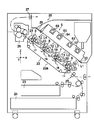
図1において、画像形成装置PRは、複数の像担持体として複数のドラム状の光導電性感光体(以下、感光体ドラム)1,2,3,4を並置したフルカラー画像形成装置であり、この4つの感光体ドラム1,2,3,4は、例えば図に対して右から順に、ブラック(BK)、シアン(C)、マゼンタ(M)、イエロー(Y)の各色に対応した画像を形成するものである(なお、色の順はこの限りではなく任意に設定することが可能である)。その4つの感光体ドラム1,2,3,4の各々の周囲には、電子写真プロセスにより画像形成を行うための、帯電部(帯電ローラ、帯電ブラシ、帯電チャージャ等)6,7,8,9と、光走査装置5からの光ビームL1,L2,L3,L4の露光部と、現像部(BK,C,M,Yの各色の現像装置)10,11,12,13と、転写搬送ベルト22a及びその裏面に配置された転写手段(転写ローラ、転写ブラシ等)14,15,16,17を備えた転写搬送装置22と、クリーニング部(クリーニングブレード、クリーニングブラシ等)18,19,20,21などが配設されており、それぞれの感光体ドラム1,2,3,4に各色の画像形成を行うことが可能となっている。
【0026】
さらに詳しくは、図1において、図中のZ方向を鉛直上方向、X,Y方向を水平方向とした場合、4つの感光体ドラム1,2,3,4の並設方向は水平面に対して傾斜しており(なお、図1の場合はX方向に対して傾斜している)、転写搬送装置22は4つの感光体ドラム1,2,3,4の並設方向と略平行となるように水平面に対して傾斜して配置され、転写材はその傾斜方向の下方側から給紙され転写搬送ベルト22aにより上方側に向けて4つの感光体ドラム1,2,3,4の転写部を順次搬送される構成であり、その転写材の搬送方向下流側で前記傾斜方向の上方側には定着装置26が配設されている。また、光走査装置5は、4つの感光体ドラム1,2,3,4が並設された作像部の斜め上方に配置され、且つ光走査装置5のハウジング50は、4つの感光体ドラム1,2,3,4の並設方向と略平行となるように水平面(図中のX方向)に対して傾斜して配置され、画像形成装置本体の傾斜したフレーム29,30に固定されている。
【0027】
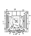
ここで、光走査装置5は、図2ないし図5に示すように、4つの光源ユニット52,53,54,55と、各光源ユニットからの光ビームL1,L2,L3,L4を対称な2方向に振り分けて偏向走査する光偏向器62と、この光偏向器62を中心にして前記2方向に対称に配置され光偏向器62により偏向走査される複数の光ビームL1,L2,L3,L4をそれぞれ対応する感光体ドラム1,2,3,4の被走査面上に導いて結像する光学系(結像用レンズ63,64,69,70,71,72、光路折り返し用ミラー65,66,67,68,73,74,75,76,77,78,79,80等の光学部材からなる)を備えており、これらの構成部材は一つのハウジング50内に収納されている。
【0028】
ハウジング50は、光偏向器62や光学系が配設される基板50Aと、基板50Aの周囲を囲む枠状の側壁50Bとを有すると共に、基板50Aが側壁50Bの略中央部に設けられてハウジング50を上下に仕切っている。4つの光源ユニット52,53,54,55はハウジング50の側壁50Bに配置され、感光体の並設方向と略同方向に並設されており、光偏向器62はハウジング50の基板50Aの略中央部に配置され、光学系を構成する光学部材(結像用レンズ63,64,69,70,71,72、光路折り返し用ミラー65,66,67,68,73,74,75,76,77,78,79,80等)は基板50Aの両面(上面側と下面側)に分けて配設されている。また、ハウジング50の上部と下部にはカバー87,88が設けられており、下部側のカバー87には光ビームを通過する開口が設けられ、その開口には防塵ガラス83,84,85,86が取り付けられている。
【0029】
この光走査装置5では、図示しない原稿読み取り装置(スキャナ)あるいは画像データ出力装置(パーソナルコンピュータ、ワードプロセッサ、ファクシミリの受信部等)から入力される色分解された画像データを光源駆動用の信号に変換し、それに従い各光源ユニット52,53,54,55内の光源(半導体レーザ(LD ))を駆動して光ビームを出射する。各光源ユニット52,53,54,55から出射された光ビームは、面倒れ補正用のシリンドリカルレンズ56,57,58,59を通り直接またはミラー60,61を介して光偏向器62に至り、ポリゴンモータ62cで等速回転されている2段のポリゴンミラー62a,62bで対称な2方向に偏向走査される。なお 、図2および図5の構成ではポリゴンミラーはL2,L3の光ビーム用と、L1,L4の光ビーム用の上下2段に分けた構成となっているが、1つの厚めのポリゴンミラーで偏向走査する構成としてもよい。
【0030】
光偏向器62のポリゴンミラー62a,62bで2ビームずつ2方向に偏向走査された光ビームは、例えば上下2層構成のfθレンズ等からなる結像用レンズ63,64をそれぞれ通過し、第1折り返しミラー65,66,67,68により折り返されて基板51の開口部を通過した後、例えば長尺トロイダルレンズ等からなる第2の結像用レンズ69,70,71,72を通過し、第2折り返しミラー73,75,77,79、第3折り返しミラー74,76,78,80、防塵ガラス83,84,85,86を介して各色用の感光体ドラム1,2,3,4の被走査面上を照射し、静電潜像を前記被走査面上に書き込む。
【0031】
なお 、前記の光走査装置5において、4つの光源ユニット52,53,54,55は、光源である半導体レーザ(LD)とその半導体レーザの出射光束をコリメートするコリメートレンズから構成され、これらがホルダ等の保持部材に一体に組み込まれた構成であるが、白黒画像形成時に多用されるブラック用の光源ユニット(例えば符号52の光源ユニット)は、白黒画像形成時の生産性の向上を目的に高速書込を可能とするために、2つ以上の光源(LD)とコリメートレンズの組を保持部材で一体に保持したマルチビーム構成とするとよい。ここで、ブラック用の光源ユニットとして用いられるマルチビーム光源ユニットの一例を図6及び図7に示す。図6はマルチビーム光源ユニットの構成を分解して示す斜視図、図7はマルチビーム光源ユニットの要部断面図である。
【0032】
図6及び図7において、光源である半導体レーザ111,112は各々支持体113,114に固定され、該支持体113,114を介して保持部材である基体(コリメートレンズホルダ)115の裏面に後述するコリメートレンズ116,117との光軸を一致させてネジ118,119等を用いて接合される。コリメートレンズ116,117は、鏡筒に収められ、コリメートレンズホルダ115の嵌合穴115a,115bに各々半導体レーザ111,112との位置を合わせて係合され、接着剤により接着されて、各光束を平行光束に変換する。また、コリメートレンズ116,117の出射側には、各々の出射光に対して所定のビーム径を得るための絞り板120が設けられており、その前方にはプリズム等で構成されるビーム合成手段121が設けられている。
【0033】
2個の半導体レーザ111,112はそのpn接合面を一致させて同一平面上に配列されており、何れか一方のビーム(本例では半導体レーザ111のビーム)は、ビーム合成手段121の入射面に貼り付けられた1/2波長板122によってその偏光面が90°回転されて、ビーム合成手段121の偏光ビームスプリッタ面121bを通過する。そして半導体レーザ112のビームは、ビーム合成手段121の斜面121aで内面反射し、ビーム合成手段121の偏光ビームスプリッタ面121bで反射して、基準となる半導体レーザ111の光軸近傍でその半導体レーザ111のビームと合成される。各半導体レーザ111,112に係わる一連のそれぞれの光軸は、互いに主走査方向に僅かにずれた位置に対応させるべく、ビーム合成手段121の出力側に示した角度θだけ互いにずらせるように設定されている。
【0034】
ビーム合成手段121と絞り板120は、フランジ部材123の裏面の所定位置に支持され、このフランジ部材123はネジ124,125により基体(コリメートレンズホルダ)115に固定される。また、フランジ部材123及び/または基体115は、半導体レーザ111,112の駆動回路が形成された基板126に図示しないネジ等により固定されていて、これにより半導体レーザ111,112からフランジ部材123に至る光路の各部材は、基板126に一体的に固定され、光源部を構成している。フランジ部材123の出射側に立設された円筒部123aは、前述した光走査装置5のハウジング50の側壁50Bに設けられている光学フレーム132の穴132aに挿通され、スプリング130の中を通り、バネ押圧板131の穴131aを通る。この状態で、半導体レーザ111,112からフランジ部材123に至るまでの各部材を基板126に組み付けたBK用の光源ユニット52を図中の矢印αの方向に引っ張り、バネ押圧板131を90°回転させることによりバネ押圧板131の突起部131bを前記円筒部123aの突起部123bに引っ掛ける。これにより、前記光学フレーム132に光源ユニット52が、フランジ部材123の円筒部123aの中心(光軸)を回転中心として回動自在に取り付けられる。
【0035】
光源ユニット52を光軸周りに回動させることにより感光体上の光スポットの間隔を変化させるピッチ可変手段の一例を以下に示す。
図6において符号127は摺動部材、128は送りネジであり、この送りネジ128には呼び径M3の雄ネジが切ってあり、摺動部材127の内側にはM3の雌ネジが切ってある。また、摺動部材127の外形は略D形状になっている。あらかじめ、摺動部材127の雌ネジ部に送りネジ128の雄ネジ部を回転挿入しておき、ハウジングの光学フレーム132側に設けた円柱132bのD形状の穴部に摺動部材127が摺動自在に挿入される。この際、光学フレーム132の前記円柱132bの穴内にはピッチ可変用ステッピングモータ129の回転軸129aが挿入されており、該回転軸129aの先端部に前記送りネジ128の下端側が圧入して固着されるようになっている。ピッチ可変用ステッピングモータ129は光学フレーム132に固定されており、該ステッピングモータ129を回転させることによりモータの回転軸129aに圧入されている送りネジ128が回転するが、この際、前記円柱132bの穴がD形状になっているため摺動部材127は回転せずに上下方向に摺動する。
【0036】
一方、光源ユニット52のフランジ部材123には、前記摺動部材127の方向に延出され、先端部で前記摺動部材127の上端に当接するアーム123cが設けられており、このアーム123cと光学フレーム132との間には引張力が付勢されたバネ135が設けられ、該バネ135によってアーム123cが下方向に引かれ、アーム123cの先端部が前記摺動部材127の平面部である斜線部に押しつけられている。よって、ピッチ可変用ステッピングモータ129の回転により前記摺動部材127が上下方向に摺動した場合、フランジ部材123のアーム123cが上下方向に揺動され、光源ユニット52は、フランジ部材123の円筒部123aの中心を回転中心として回転する。
【0037】
また、光源ユニット52の回転角を制御する手段として、ハウジングの光学フレーム132側には発光部133aと受光部133bを備えたフォトインタラプタからなる光学式のホームポジションセンサ133が図示しないネジ等により固定されており、かつ、フランジ部材123のアーム132bと反対側の一部には、前記ホームポジションセンサ133の発光部133aと受光部133bの間を遮蔽可能なエッジ部123eを有するフィラー123dが設けられている。そして、フランジ部材123のフィラー123dのエッジ部123eが、ホームポジションセンサ133の発光部133aと受光部133bの間を遮蔽した瞬間の位置がホームポジション(H.P.)位置となるように設定されており、回転調整の基準となっている。
【0038】
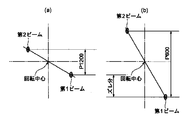
図6及び図7に示す光源ユニット52の回転調整により副走査方向のピッチを変更するための構成を図8に示す。図8においては、破線でホームポジションセンサ133の発光部133aと受光部133bの位置を示しており、前述のようにフランジ部材123に設けた遮蔽用のフィラー123dのエッジ部123eが発光部133aと受光部133bの間を遮蔽した瞬間の位置がホームポジション(H.P.)位置である。また図中のポジションBは、光源ユニット52がホームポジション(H.P.)より光軸を回転中心としてθ1回転した位置であるが、この回転角を得るためピッチ可変用ステッピングモータ129は所定のパルス数回転し、前述の摺動部材127を上方向に所定量移動させ、光源ユニット52を回転させる。同様に図中のポジションAは、光源ユニット52がホームポジション(H.P.)より光軸を回転中心としてθ2回転した位置である。
【0039】
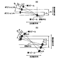
ここで図9は、前記のホームポジション(H.P.)及びポジションA,Bのときの2つの光スポットの感光体上の位置の一例を示したものであり、同図(a)は2つの半導体レーザからのビームのうち一方のビームの位置を回転中心に合わせて回転調整する場合の例、(B)は2つのビーム間の中央の位置を回転中心として回転調整する場合の例を示しており、回転角θ1,θ2に対応した感光体上の光スポットの副走査方向のピッチがP1,P2となる。すなわち、ホームポジション(H.P.)からの回転量を変化させることにより感光体上の光スポットの間隔(ピッチ)を変えることができ、回転量は前記ステッピングモータ129のH.P.からの駆動パルス数により容易に制御できる。
【0040】
通常の場合、記録密度に応じて感光体上の光スポットの副走査方向のピッチを変化させるわけであるが、例えば記録密度600dpiのときのピッチ:P=42μmに設定するときのH.P.からのパルス数:Paと、記録密度1200dpiのときの副走査方向のピッチ:P=21μmに設定するときのH.P.からのパルス数:Pbとをそれぞれ画像形成装置内の制御部のメモリ等にて記憶しておけば、画像形成時の要求記録密度に応じて前記ステッピングモータ129を回転させ、感光体上の光スポットの副走査方向のピッチを容易に切換えることができる。
【0041】
なお、通常、画像形成装置の電源投入時に光源ユニット52は予め決められた位置、例えば600dpiの記録密度時の回転角(ポジションB)に回転制御される。これは、電源投入時に一度H.P.位置にホーミングした後、ステッピングモータ129を所定の方向にパルス数Pa駆動し、感光体上の光スポットの副走査方向のピッチがPになるように光源ユニット52が回転される。その後、光源ユニット52の回転角は制御部のCPU(中央演算処理装置)内等のメモリにて認識されており、記録密度1200dpiが要求されたときは600dpi時の位置(ポジションB)よりステッピングモータ129を[Pb−Pa]のパルス数だけ回転させることにより感光体上の光スポットのピッチPを1200dpiの位置(ポジションA)に変えることができる。
【0042】
このときの処理手順の一例を図10のフローチャートに示す。この処理では、ユーザがブラックモードで1200dpiの書き込み密度を選択すると(ステップS1)、BKビームピッチポジションがポジションAであるかどうかをチェックする(ステップS2)。ポジションAにいれば、送られてくる書き込みデータを蓄積した後、ポリゴンモータ62cを回転させて通常のプリント動作を実行する(ステップS3)。一方、ポジションAにいなければ、BKピームピッチポジションのAに移動を開始する(ステップS4)。そして、ステッピングモータ129を前記[Pb−Pa]のパルス数だけ回転させ、ポジションAへの移動が終了した時点で(ステップS6)、1200dpiの正規位置での書き込みが可能なので、ステップS3の処理を実行し、一連の書き込み処理を終える(ステップS7)。なお、ステップS3の終了時点では、BKのビームポジションはAである。
【0043】
もし、この状態でユーザがカラーモードで600dpiのプリントを選択すると(ステップS8)、BKビームポジションがBであるかどうかをチェックする(ステップS9)。この場合、前述のようにステップS3の終了時点でビームポジションはAであるので、通常、ステップS9の判定はNOである。そこで、BKビームピッチポジションをBに移動させるべくステッピングモータ129を[Pb−Pa]のパルス数だけステップS5とは逆方向に回転させてBKのビームポジションを移動指せ(ステップS11,S12)、ポジジョンBへの移動が終了した時点で(ステップS13)、送られてくる書き込みデータを蓄積した後、ポリゴンモータ62cを回転させて通常のプリント動作を実行し(ステップS10)、一連の書き込み処理を終える(ステップS14)。
【0044】
なお、このような切り換え制御は、プリンタドライバでユーザが選択し、あるいは送られてきたデータあるいは指示に応じてプリンタドライバが自動的に処理し、所望の書き込み密度の画像がプリントアウトされる。
【0045】
図2ないし5に示す構成の光走査装置2においては、各光ビームL1,L2,L3,L4の光路には、主走査方向の走査開始位置の光束を取り出すための図示しない同期検知用ミラーが設けられており、同期検知用ミラーで反射された光束は、図5中に破線で示すように同期検知器81,82で受光されて走査開始の同期信号が出力される。また、図5に示すように、L1,L2,L3の光ビームの光路に配置された第3折り返しミラー74,76,78にはスキュー調整用のステッピングモータ92,93,94が設けられており、L1の光ビームの走査線位置を基準にして、L1,L2,L3の光ビームの走査線位置のずれを補正している。なお、光偏向器62によって偏向走査される光ビームの走査方向が主走査方向であり、これは各感光体ドラムの軸方向である。また、この主走査方向に直交する方向が副走査方向であり、これは感光体ドラムの回転方向(感光体ドラム表面の移動方向)であり、さらには後述する転写搬送ベルト22aの搬送方向である。すなわち転写搬送ベルト22aの幅方向が主走査方向、搬送方向が副走査方向となる。
【0046】
図1に示すように、並設された4つの感光体ドラム1,2,3,4の下には駆動ローラと複数の従動ローラに張架された転写搬送ベルト22aが配設されており、駆動ローラにより図中に矢印で示す方向に搬送されている。また、画像形成装置の本体下部には記録用紙等の転写材を収納した複数の給紙部23,24が設置されており、この給紙部23,24に収納された転写材が、給紙ローラ、搬送ローラ、レジストローラ25を介して転写搬送ベルト22aに給紙され、転写搬送ベルト22aにより担持され搬送される。
【0047】
前記光走査装置5により各感光体1,2,3,4に形成された各潜像は、各現像部10,11,12,13のBK,C,M,Yの各色のトナーで現像されて顕像化され、その顕像化されたBK,C,M,Yの各色のトナー画像は、転写搬送装置22の各転写手段14,15,16,17により転写搬送ベルト22a上に担持された転写材に順次重ね合わせて転写される。そして、4色の画像が転写された転写材は定着装置26に搬送され、定着装置26で画像が定着された後、排紙ローラ27により排紙トレイ28上に排出される。なお、白黒画像形成モードの時は、ブラック用の感光体ドラム1のみに対して上述の作像動作が行われる。
【0048】
以上、本発明に係る画像形成装置の構成・動作について説明したが、フルカラー画像の主走査、副走査方向レジスト調整時は(600dpi、1200dpiに関わらず)ブラックの画素密度位置を一定の画素密度位置にて書き込み調整し、フルカラー出力時(600dpi、1200dpiに関わらず)のブラックの画素密度位置を前記調整時の画素密度位置にて書き込むことにより位置ずれのない、タンデム式のカラー画像形成装置を達成することができる。
【0049】
なお、この実施形態では、書き込み密度を600dpiおよび1200dpiとで切り換えることができる光走査装置及び画像形成装置について説明しているが、600dpi、1200dpiに加え2400dpiの場合も同様に構成することができる。
【0050】
【発明の効果】
以上のように、本発明によれば、フルカラー画像の主走査、副走査方向レジスト調整時は前記ブラック書き込み用光源の画素密度位置を一定の画素密度位置に設定して書き込み調整を行い、フルカラー画像出力時には、前記ブラック書き込み用光源の画素密度位置を前記書き込み調整を行った位置に設定して書き込むので、2ビームのブラック書き込み用光源書き込み密度を切り換えてフルカラーの画像を書き込む際に光書き込みに起因する位置ずれや色ずれの発生を防止することができる。
【0051】
また、フルカラーとモノクロの出力枚数に応じてが画素密度を切り換えることにより高画質モード、速度優先モードを選択することが可能になり、これによりフルカラーのモノクロに応じて出力効率と画質を両者の要求を満たすことができる。
【図面の簡単な説明】
【図1】本発明の一実施形態に係る画像形成装置の概略構成を示す図である。
【図2】図1に示す画像形成装置に備えられる光走査装置の基板上面側の構成を示す平面図である。
【図3】図2に示す光書込装置のA−A線断面図である。
【図4】図2に示す光走査装置の構成から光源ユニット、光偏向器及び光学系を抜き出してその配置構成を示した説明図である。
【図5】図3に示す光走査装置の構成から光偏向器及び光学系を抜き出してその配置構成を示した説明図である。
【図6】本発明の実施形態に係るマルチビーム光源ユニットの構成を分解して示す斜視図である。
【図7】本発明の実施形態に係るマルチビーム光源ユニットの要部断面図である。
【図8】光源ユニットの回転調整により副走査方向のピッチを変更する構成を示す図である。
【図9】光源ユニットのホームポジション及びポジションA,Bのときの2つの光スポットの感光体上の位置を示す図である。
【図10】光源ユニットのポジションA,Bの変更時の処理手順の一例を示すフローチャートである。
【図11】画素密度の違いによる2ビーム光書き込みの書き込み位置の違いを示す図である。
【図12】ドット位置のずれと副走査方向のずれとの関係を示す図である。
【図13】ドット位置のずれと主走査方向のずれとの関係を示す図である。
【符号の説明】
1,2,3,4 感光体ドラム
5 光走査装置
50 ハウジング
52,53,54,55 光源ユニット
62 光偏光器
111,112 半導体レーザ
115 基体(コリメートレンズホルダ)
120 絞り板
121 ビーム合成手段
123 フランジ部材
123a 円筒部
123c アーム
123d フィラー
126 基板
127 摺動部材
128 送りネジ
129 ステッピングモータ
132 光学フレーム
133 ホームポジションセンサ[0001]
TECHNICAL FIELD OF THE INVENTION
The present invention is directed to an optical scanning method and an optical scanning device for writing a latent image by irradiating a light beam on a surface to be scanned of a plurality of image carriers arranged in parallel, and forming on the plurality of image carriers by the optical scanning device. The present invention relates to an image forming apparatus, such as a copying machine, a printer, a facsimile, and a plotter, that develops a latent image formed with a developer of a different color, and sequentially transfers the latent image to a transfer material to form a multicolor image.
[0002]
[Prior art]
2. Description of the Related Art Conventionally, light beams emitted from a plurality of light sources are applied to four image carriers (for example, photosensitive drums) arranged in parallel to write a latent image, and latent images formed on each image carrier are written. The image is developed with a developer of a different color (for example, yellow, magenta, cyan, or black toner) to form a visible image, and then a transfer material such as a recording sheet carried on a transfer conveyance belt or the like is transferred to each image bearing member. The images are sequentially transferred to the transfer section of the body, and after the visible images of each color formed on each image carrier are superimposed on the transfer material and transferred, the image transferred on the transfer material is fixed to form a multicolor image. A tandem-type color image forming apparatus to be obtained is known.
[0003]
In such a tandem-type color image forming apparatus, a type in which a latent image is written on each image carrier separately by an optical writing device individually provided for each image carrier is conventionally known. An optical writing device using an optical deflector composed of a polygon mirror and a motor for driving the polygon mirror is relatively expensive. Providing an optical writing device for each image carrier individually in terms of component costs and manufacturing costs. There's a problem. In addition, a large installation space is required to install a plurality of optical writing devices having an optical deflector in accordance with the number of image carriers, and thus there is a problem that the entire image forming apparatus becomes large.
[0004]
Furthermore, although a tandem-type color image forming apparatus is used, in a general office, there is a considerable amount of output of a monochrome-only document in addition to the output of a full-color document. In addition, a tandem-type color image forming apparatus has a greater number of full-color output sheets, or has a higher output speed,
{Circle around (1)} A four-color superposition mechanism becomes complicated.
{Circle around (2)} The cost of driving parts such as a motor and a photoconductor increases.
{Circle around (3)} The life of driving parts such as a motor and a photoconductor is shortened.
(4) The machine size increases.
Therefore, for the above-mentioned office users, the productivity in the monochrome mode was higher than the productivity in the full color mode, in other words, the linear speed in the monochrome mode was higher than the linear speed in the full color mode. Image forming apparatuses are also used. In such an image forming apparatus, the monochrome output number is faster than the full color output number, that is, the image formation number per unit time is larger.
[0005]
Also, among the functions of one full-color image forming apparatus, 1200 dpi (a configuration in which the writing density is increased by lowering the linear velocity) in which the number of output is reduced but the image quality is emphasized, or the number of output is increased but the image quality is slightly reduced There is also a machine capable of switching such as 600 dpi (a configuration in which the linear velocity is increased and the pixel density is reduced).
[0006]
[Problems to be solved by the invention]
As described above, in a machine in which the high image quality mode and the speed priority mode can be selected by switching the pixel density so that the number of monochrome output is larger than the number of full color output, the BK (black) beam is used. There is a two-beam and pitch switching mechanism. The color (Y, M, C) beam is composed of one beam, and when priority is given to monochrome 1200 dpi image quality, two-beam writing is performed. The linear velocity of the BK2 beam is 1200 dpi, the monochrome speed is 600 dpi. Priority is 2-beam writing, linear speed is fast, sub-scanning is 600 dpi pitch, and color 1200 dpi image quality is BK1 beam (only one of the two beams is turned on, and color is one beam), and linear speed is slow. When sub-scanning of one beam is 1200 dpi and color is 600 dpi, priority is given to BK1 beam (one beam out of two beams). Munomi lighting, for color 1 beam), the linear velocity is fast a configuration such subscanning 600dpi for each color one beam.
[0007]
In this case, the pixel density switching position of the BK is fixed to either 600 dpi or 1200 dpi when adjusting the registration position in the main scanning and sub-scanning directions of the four colors (BK, C, M, Y) (BK uses only one beam). Otherwise, the BK writing position may shift during full-color output, resulting in a color shift. This example is shown in FIG. FIGS. 10A and 10B are diagrams showing the states of the writing dots of the light beams of 1200 dpi and 600 dpi in the two-beam writing. FIG. 11A shows the state of the first beam and the second beam at the time of 1200 dpi, and FIG. The state of the first beam and the second beam at 600 dpi is shown. As can be seen from these figures, at 1200 dpi in the sub-scanning direction,
25.4 mm / 1200 = 21 μm
At 600 dpi,
25.4 mm / 600 = 42 μm
As can be seen from FIG. 11, at 1200 dpi and 600 dpi, the dot position is
L = (42-21) /2=10.5 μm
Will be shifted. Therefore, when writing in full color as shown in FIG. 12, BK also performs one-beam writing. Therefore, if the beam pitch position is not managed at 1200 dpi and 600 dpi, BK and another color (here, cyan C ) Is narrowed, and a deviation from other colors occurs in the sub-scanning direction.
[0008]
On the other hand, when a full-color image is formed with the second beam despite the use of the first beam as shown in FIG. 13A for the adjustment in full color, as shown in FIG. Misalignment occurs. This shift comes from the difference in the BK dot positions as described above (FIG. 13C). Note that the term “at the time of adjustment” as used herein means an adjustment for correcting color misregistration occurring at the time of shipment from a factory or during normal use by a user, and is disclosed in, for example, Japanese Patent Application Laid-Open No. H11-301032. It is a technology that has been.
[0009]
The present invention has been made in view of such a situation of the related art, and an object of the present invention is to provide a function having a function of switching a writing density by using a BK2 beam, in which a displacement occurs when writing a full-color image by switching the writing density. An object of the present invention is to provide an optical scanning device that does not generate any light.
[0010]
Another object of the present invention is to provide an image forming apparatus which does not cause color shift when writing a full-color image by switching the writing density.
[0011]
[Means for Solving the Problems]
In order to achieve the above object, the first means includes a light source for black writing that performs optical writing at a plurality of pixel densities, and a light source for color writing that performs optical writing at a preset one pixel density. In the optical scanning method of performing an optical scan on a forming medium to write an image, a main scan of a full-color image, and a pixel density position of the black writing light source are set to a constant pixel density position during registration adjustment in the sub-scanning direction. The writing adjustment is performed, and when a full-color image is output, writing is performed by setting the pixel density position of the black writing light source to the position where the writing adjustment is performed.
[0012]
When writing in this way, when writing a full-color image, when changing the pixel density or changing the writing speed, writing is always performed at the pixel density position adjusted for full color, so the writing position shift No color misregistration occurs due to this.
[0013]
The second means includes a light source for black writing that performs optical writing at a plurality of pixel densities, and a light source for color writing that performs optical writing at one preset pixel density, and performs optical scanning on an image forming medium. In the optical scanning device that writes an image by performing the main scanning of a full-color image, a storage unit that stores a pixel density position of the black writing light source set at the time of registration adjustment in the sub-scanning direction, and a storage unit that outputs a full-color image. Switching control means for switching the writing position to the stored pixel density position at the time of the registration adjustment, and when outputting a full-color image, the switching control means changes the pixel density position of the black writing light source to the position at which the writing adjustment was performed. Switching to the main scanning and sub-scanning registration positions to perform optical writing. And butterflies.
[0014]
With this configuration, when writing an image in full color, the writing position of the black writing light source is switched to the state at the time of shipment from the factory or when normal adjustment is performed to correct the color misregistration that occurred during use. Since optical writing is performed, even if the writing density and the writing speed are different from those at the time of adjustment, color shift does not occur due to the shift of the writing position at the time of full-color writing.
[0015]
The third means is the second means, wherein the black writing light source comprises at least two semiconductor lasers, holding means for holding these semiconductor lasers in a relatively constant state, and It is characterized by comprising a supporting means for rotatably supporting the set rotation center and a driving means for rotating the holding means about the rotation center.
[0016]
With such a configuration, the black writing light source is constituted by two beams, and the writing position of the two beams can be easily adjusted by setting the rotation position.
[0017]
A fourth means is the third means, wherein the driving means comprises a stepping motor. When the driving means is constituted by a stepping motor in this manner, the rotation angle can be set by the number of steps, so that the rotation angle control can be performed easily and easily.
[0018]
Fifth means is the fourth means, wherein the switching control means drives the stepping motor to switch to a pixel density position stored in the storage means. With this configuration, when performing full-color image formation, switching of pixel density can be automatically performed by the switching control unit.
[0019]
A sixth means is the third means, wherein the black writing light source comprises two semiconductor lasers, and the rotation center bisects a line connecting the laser beam writing positions of the two semiconductor lasers. Or a position corresponding to one of the writing positions of the laser beam. With this configuration, since the rotation angle and the writing position can be relatively defined with reference to the rotation center, the writing position can be easily set to a desired position by setting the relationship between the plurality of writing positions and the rotation angle in advance. Can be changed to
[0020]
The seventh means includes an optical scanning device according to the second to sixth means, and an image forming means for visualizing an image written for each color by the optical scanning device to form a color image on a recording medium. And that the image forming apparatus is configured. With this configuration, a full-color image written by the second to sixth means can be formed without color shift.
[0021]
Eighth means is the seventh means, wherein the optical scanning device performs optical writing for each color on an image carrier arranged in parallel for each color. When writing is performed on the image carriers that are arranged in parallel for each color in this manner, it is possible to suppress the occurrence of color misregistration when forming a full-color image in a so-called tandem-type image forming apparatus. That is, a plurality of light source units for black (two or more beams) and one for color (one beam) having a pixel density switching means are provided, and a light beam is formed on a surface to be scanned of a plurality of image carriers of a tandem type image forming apparatus. When writing a latent image by irradiating the image, writing adjustment of the black pixel density position at a fixed pixel density position (regardless of 600 dpi, 1200 dpi, and 2400) during registration adjustment in the main scanning and sub-scanning directions of a full-color image In addition, since the black pixel density position at the time of full color output (regardless of 600 dpi, 1200 dpi, and 2400) is written at the pixel density position at the time of the adjustment, no color shift occurs due to a shift in the writing position.
[0022]
Further, a plurality of light source units for black (two or more beams) and one for color (one beam) having a pixel density switching means are provided, and when the registration of the full-color image in the main scanning and sub-scanning directions is adjusted (regardless of 600 dpi or 1200 dpi). The black pixel density position is written and adjusted at a fixed pixel density position, and the black pixel density position at the time of full color output (regardless of 600 dpi and 1200 dpi) is written at the pixel density position at the time of the adjustment. The high image quality mode and the speed priority mode can be selected by switching the pixel density so that the monochrome output number becomes faster than the image number.
[0023]
BEST MODE FOR CARRYING OUT THE INVENTION
Hereinafter, embodiments of the present invention will be described with reference to the drawings.
[0024]
FIG. 1 is a diagram showing a schematic configuration of an image forming apparatus according to an embodiment of the present invention, FIG. 2 is a plan view showing a configuration of an optical scanning device provided in the image forming apparatus shown in FIG. FIG. 4 is a cross-sectional view taken along line AA of the optical writing device shown in FIG. 2; FIG. 4 is an explanatory diagram showing an arrangement configuration of a light source unit, an optical deflector, and an optical system extracted from the configuration of the optical scanning device shown in FIG. FIG. 5 is an explanatory diagram showing an arrangement configuration of an optical deflector and an optical system extracted from the configuration of the optical scanning device shown in FIG.
[0025]
In FIG. 1, an image forming apparatus PR is a full-color image forming apparatus in which a plurality of drum-shaped photoconductive photoconductors (hereinafter, photoconductor drums) 1, 2, 3, and 4 are arranged as a plurality of image carriers, The four
[0026]
More specifically, in FIG. 1, when the Z direction in the figure is a vertically upward direction and the X and Y directions are horizontal directions, the direction in which the four
[0027]
Here, as shown in FIGS. 2 to 5, the
[0028]
The
[0029]
The
[0030]
The light beams deflected and scanned in two directions by two beams by the polygon mirrors 62a and 62b of the
[0031]
In the
[0032]
6 and 7,
[0033]
The two
[0034]
The beam combining means 121 and the
[0035]
An example of a pitch changing unit that changes the interval between light spots on the photoconductor by rotating the
In FIG. 6,
[0036]
On the other hand, the
[0037]
As a means for controlling the rotation angle of the
[0038]
FIG. 8 shows a configuration for changing the pitch in the sub-scanning direction by adjusting the rotation of the
[0039]
FIG. 9 shows an example of the positions of the two light spots on the photoreceptor at the home position (HP) and the positions A and B. FIG. (B) shows an example in which the rotation of one of the beams from two semiconductor lasers is adjusted to the center of rotation, and (B) shows an example of the case in which the center of the position between the two beams is adjusted as the center of rotation. The pitch of the light spot on the photoconductor in the sub-scanning direction corresponding to the rotation angles θ1 and θ2 is P1 and P2. That is, by changing the rotation amount from the home position (HP), the interval (pitch) between the light spots on the photoconductor can be changed. P. Can be easily controlled by the number of drive pulses from
[0040]
In the normal case, the pitch of the light spot on the photoconductor in the sub-scanning direction is changed according to the recording density. For example, the pitch when the recording density is 600 dpi: P = 42 μm. P. : Pa and the pitch in the sub-scanning direction at a recording density of 1200 dpi: P = 21 μm. P. Is stored in a memory or the like of a control unit in the image forming apparatus, the stepping
[0041]
Normally, when the power of the image forming apparatus is turned on, the
[0042]
An example of the processing procedure at this time is shown in the flowchart of FIG. In this process, when the user selects a writing density of 1200 dpi in the black mode (step S1), it is checked whether the BK beam pitch position is at position A (step S2). If it is in the position A, after storing the sent write data, the
[0043]
If the user selects printing at 600 dpi in the color mode in this state (step S8), it is checked whether the BK beam position is B (step S9). In this case, since the beam position is A at the end of step S3 as described above, the determination in step S9 is normally NO. Then, in order to move the BK beam pitch position to B, the stepping
[0044]
Note that such switching control is selected by the user with the printer driver, or is automatically processed by the printer driver in accordance with the transmitted data or instruction, and an image having a desired writing density is printed out.
[0045]
In the
[0046]
As shown in FIG. 1, a
[0047]
Each of the latent images formed on each of the
[0048]
While the configuration and operation of the image forming apparatus according to the present invention have been described above, the black pixel density position (regardless of 600 dpi and 1200 dpi) is set to a fixed pixel density position during registration adjustment in the main scanning and sub-scanning directions of a full-color image. A tandem-type color image forming apparatus that is free from misalignment by writing the black pixel density position at full color output (regardless of 600 dpi and 1200 dpi) at the pixel density position at the time of the adjustment is achieved. can do.
[0049]
In this embodiment, an optical scanning device and an image forming apparatus capable of switching the writing density between 600 dpi and 1200 dpi are described. However, the same configuration can be applied to 2400 dpi in addition to 600 dpi and 1200 dpi.
[0050]
【The invention's effect】
As described above, according to the present invention, at the time of registration adjustment in the main scanning and sub-scanning directions of a full-color image, writing adjustment is performed by setting the pixel density position of the black writing light source to a constant pixel density position, and the full-color image is adjusted. At the time of output, writing is performed by setting the pixel density position of the black writing light source to the position where the writing adjustment has been performed, so that when writing a full-color image by switching the two-beam black writing light source writing density, light writing may occur. It is possible to prevent the occurrence of misalignment or color misalignment.
[0051]
In addition, by switching the pixel density according to the number of full-color and monochrome output sheets, it is possible to select a high-quality mode or speed priority mode, which requires both output efficiency and image quality according to full-color monochrome. Can be satisfied.
[Brief description of the drawings]
FIG. 1 is a diagram illustrating a schematic configuration of an image forming apparatus according to an embodiment of the present invention.
FIG. 2 is a plan view showing a configuration on an upper surface side of a substrate of an optical scanning device provided in the image forming apparatus shown in FIG.
FIG. 3 is a sectional view taken along line AA of the optical writing device shown in FIG. 2;
FIG. 4 is an explanatory diagram showing an arrangement configuration of a light source unit, an optical deflector, and an optical system extracted from the configuration of the optical scanning device shown in FIG. 2;
FIG. 5 is an explanatory diagram showing an arrangement configuration of an optical deflector and an optical system extracted from the configuration of the optical scanning device shown in FIG. 3;
FIG. 6 is an exploded perspective view showing a configuration of a multi-beam light source unit according to the embodiment of the present invention.
FIG. 7 is a sectional view of a main part of the multi-beam light source unit according to the embodiment of the present invention.
FIG. 8 is a diagram showing a configuration for changing a pitch in the sub-scanning direction by adjusting the rotation of a light source unit.
FIG. 9 is a diagram illustrating positions of two light spots on a photoconductor at a home position and positions A and B of the light source unit.
FIG. 10 is a flowchart illustrating an example of a processing procedure when changing positions A and B of the light source unit.
FIG. 11 is a diagram illustrating a difference in a writing position in two-beam light writing due to a difference in pixel density.
FIG. 12 is a diagram showing a relationship between a dot position shift and a sub-scan direction shift.
FIG. 13 is a diagram illustrating a relationship between a shift in dot position and a shift in the main scanning direction.
[Explanation of symbols]
1,2,3,4 photosensitive drum
5 Optical scanning device
50 Housing
52,53,54,55 Light source unit
62 Optical Polarizer
111,112 Semiconductor laser
115 Substrate (collimating lens holder)
120 Aperture plate
121 beam combining means
123 Flange member
123a cylindrical part
123c arm
123d filler
126 substrate
127 sliding member
128 feed screw
129 Stepping motor
132 Optical Frame
133 Home position sensor
Claims (8)
フルカラー画像の主走査、副走査方向レジスト調整時は前記ブラック書き込み用光源の画素密度位置を一定の画素密度位置に設定して書き込み調整を行い、
フルカラー画像出力時には、前記ブラック書き込み用光源の画素密度位置を前記書き込み調整を行った位置に設定して書き込むことを特徴とする光走査方法。A black writing light source that performs optical writing at a plurality of pixel densities and a color writing light source that performs optical writing at one preset pixel density are provided, and an image is written by performing optical scanning on an image forming medium. In the optical scanning method,
At the time of registration adjustment in the main scanning and sub-scanning directions of a full-color image, writing adjustment is performed by setting the pixel density position of the black writing light source to a fixed pixel density position,
When outputting a full-color image, writing is performed by setting the pixel density position of the black writing light source to the position where the writing adjustment has been performed.
フルカラー画像の主走査、副走査方向レジスト調整時に設定した前記ブラック書き込み用光源の画素密度位置を記憶する記憶手段と、
フルカラー画像出力時には、前記記憶手段に記憶された前記レジスト調整時の画素密度位置に書き込み位置を切り換える切り換え制御手段と、
を備え、
フルカラー画像出力時には、前記切り換え制御手段は、前記ブラック書き込み用光源の画素密度位置を前記書き込み調整を行った位置に切り換えて光書き込みを行うことを特徴とする光走査装置。A black writing light source that performs optical writing at a plurality of pixel densities, and a color writing light source that performs optical writing at one preset pixel density are provided, and an image is written by performing optical scanning on an image forming medium. In an optical scanning device,
Main scanning of a full-color image, storage means for storing the pixel density position of the black writing light source set at the time of registration adjustment in the sub-scanning direction,
At the time of full color image output, switching control means for switching the writing position to the pixel density position at the time of the registration adjustment stored in the storage means,
With
The optical scanning device according to claim 1, wherein, when outputting a full-color image, the switching control unit switches the pixel density position of the black writing light source to the position where the writing adjustment has been performed to perform optical writing.
少なくとも2個の半導体レーザと、
これらの半導体レーザを相対的に一定の状態で保持する保持手段と、
前記保持手段をあらかじめ設定された回転中心に関して回転可能に支持する支持手段と、
前記保持手段を前記回転中心に関して回転させる駆動手段と、
を含んでなることを特徴とする請求項2記載の光走査装置。The black writing light source,
At least two semiconductor lasers;
Holding means for holding these semiconductor lasers in a relatively constant state,
Support means for rotatably supporting the holding means about a preset center of rotation,
Driving means for rotating the holding means about the rotation center,
The optical scanning device according to claim 2, comprising:
前記光走査装置によって各色毎に書き込まれた画像を顕像化して記録媒体上にカラー画像を形成する画像形成手段と、
を含んで構成されていることを特徴とする画像形成装置。An optical scanning device according to any one of claims 2 to 6,
Image forming means for visualizing an image written for each color by the optical scanning device to form a color image on a recording medium,
An image forming apparatus comprising:
Priority Applications (4)
| Application Number | Priority Date | Filing Date | Title |
|---|---|---|---|
| JP2002169989A JP2004013074A (en) | 2002-06-11 | 2002-06-11 | Optical scanning method, optical scanner, and image forming device |
| US10/452,458 US6930700B2 (en) | 2002-06-11 | 2003-06-02 | Optical scanning method, optical scanner and image forming apparatus |
| EP03253566A EP1372337A1 (en) | 2002-06-11 | 2003-06-05 | Optical scanning method, optical scanner and image forming apparatus |
| US11/142,131 US7593028B2 (en) | 2002-06-11 | 2005-05-31 | Optical scanning method, optical scanner and image forming apparatus |
Applications Claiming Priority (1)
| Application Number | Priority Date | Filing Date | Title |
|---|---|---|---|
| JP2002169989A JP2004013074A (en) | 2002-06-11 | 2002-06-11 | Optical scanning method, optical scanner, and image forming device |
Publications (1)
| Publication Number | Publication Date |
|---|---|
| JP2004013074A true JP2004013074A (en) | 2004-01-15 |
Family
ID=29561745
Family Applications (1)
| Application Number | Title | Priority Date | Filing Date |
|---|---|---|---|
| JP2002169989A Pending JP2004013074A (en) | 2002-06-11 | 2002-06-11 | Optical scanning method, optical scanner, and image forming device |
Country Status (3)
| Country | Link |
|---|---|
| US (2) | US6930700B2 (en) |
| EP (1) | EP1372337A1 (en) |
| JP (1) | JP2004013074A (en) |
Cited By (1)
| Publication number | Priority date | Publication date | Assignee | Title |
|---|---|---|---|---|
| JP2007298701A (en) * | 2006-04-28 | 2007-11-15 | Ricoh Co Ltd | Optical scanner and image forming apparatus |
Families Citing this family (9)
| Publication number | Priority date | Publication date | Assignee | Title |
|---|---|---|---|---|
| JP2004354848A (en) * | 2003-05-30 | 2004-12-16 | Ricoh Co Ltd | Optical scanner and image forming apparatus |
| JP4238866B2 (en) * | 2005-11-28 | 2009-03-18 | コニカミノルタビジネステクノロジーズ株式会社 | Image forming apparatus |
| US7548252B2 (en) * | 2006-02-16 | 2009-06-16 | Canon Kabushiki Kaisha | Optical scanning apparatus and color image forming apparatus using the same |
| JP4980678B2 (en) * | 2006-09-06 | 2012-07-18 | 株式会社リコー | Optical scanning device, optical scanning device manufacturing method, and color image forming apparatus |
| JP2009012323A (en) * | 2007-07-05 | 2009-01-22 | Konica Minolta Business Technologies Inc | Image forming device, image forming method, and program |
| JP5266798B2 (en) * | 2008-03-04 | 2013-08-21 | 株式会社リコー | Optical scanning apparatus and image forming apparatus |
| JP5397282B2 (en) | 2010-03-17 | 2014-01-22 | 株式会社リコー | Misalignment correction apparatus and image forming apparatus having the same |
| US8771085B1 (en) | 2010-08-06 | 2014-07-08 | Arthur C. Clyde | Modular law enforcement baton |
| JP5124000B2 (en) * | 2010-09-06 | 2013-01-23 | シャープ株式会社 | Image forming apparatus |
Family Cites Families (16)
| Publication number | Priority date | Publication date | Assignee | Title |
|---|---|---|---|---|
| JPS6413132A (en) | 1987-06-15 | 1989-01-18 | Sharp Kk | Automatic original conveying device |
| JPH0343707A (en) | 1989-07-11 | 1991-02-25 | Canon Inc | Scanning optical device |
| US5351070A (en) | 1992-01-24 | 1994-09-27 | Xerox Corporation | Single pass color printer having improved process and slow registration |
| US5786594A (en) | 1996-01-18 | 1998-07-28 | Ricoh Company, Ltd. | Multi-beam pitch adjustment system and method |
| JP3437025B2 (en) | 1996-01-19 | 2003-08-18 | 株式会社リコー | Multi-beam scanner |
| JPH1039241A (en) | 1996-07-19 | 1998-02-13 | Konica Corp | Laser recording device |
| JP3708661B2 (en) | 1997-02-28 | 2005-10-19 | 株式会社リコー | Color image forming apparatus |
| US6163333A (en) * | 1998-03-27 | 2000-12-19 | Matsushita Electric Industrial Co., Ltd. | Multi-beam scanning optical apparatus |
| JPH11301032A (en) | 1998-04-17 | 1999-11-02 | Ricoh Co Ltd | Image forming apparatus |
| JP2000280523A (en) * | 1999-03-30 | 2000-10-10 | Ricoh Co Ltd | Image forming apparatus |
| JP3668053B2 (en) | 1999-06-28 | 2005-07-06 | 株式会社リコー | Multi-beam scanning apparatus and image forming apparatus |
| JP3980824B2 (en) | 2000-11-07 | 2007-09-26 | 株式会社リコー | Optical writing apparatus and image forming apparatus |
| JP3862951B2 (en) | 2000-11-29 | 2006-12-27 | 株式会社リコー | Molding method of housing |
| US6528047B2 (en) * | 2001-04-18 | 2003-03-04 | Goldschmidt Chemical Corporation | Odor absorption and deodorization |
| JP4322442B2 (en) | 2001-05-18 | 2009-09-02 | 株式会社リコー | Image forming apparatus |
| JP4521800B2 (en) | 2001-07-19 | 2010-08-11 | 株式会社リコー | Image forming apparatus |
-
2002
- 2002-06-11 JP JP2002169989A patent/JP2004013074A/en active Pending
-
2003
- 2003-06-02 US US10/452,458 patent/US6930700B2/en not_active Expired - Fee Related
- 2003-06-05 EP EP03253566A patent/EP1372337A1/en not_active Ceased
-
2005
- 2005-05-31 US US11/142,131 patent/US7593028B2/en not_active Expired - Fee Related
Cited By (1)
| Publication number | Priority date | Publication date | Assignee | Title |
|---|---|---|---|---|
| JP2007298701A (en) * | 2006-04-28 | 2007-11-15 | Ricoh Co Ltd | Optical scanner and image forming apparatus |
Also Published As
| Publication number | Publication date |
|---|---|
| EP1372337A1 (en) | 2003-12-17 |
| US7593028B2 (en) | 2009-09-22 |
| US20030226959A1 (en) | 2003-12-11 |
| US6930700B2 (en) | 2005-08-16 |
| US20050219351A1 (en) | 2005-10-06 |
Similar Documents
| Publication | Publication Date | Title |
|---|---|---|
| JP5033548B2 (en) | Optical writing apparatus and image forming apparatus | |
| US7593028B2 (en) | Optical scanning method, optical scanner and image forming apparatus | |
| JP3980826B2 (en) | Optical writing apparatus and image forming apparatus | |
| JP2000280523A (en) | Image forming apparatus | |
| US7471307B2 (en) | Image forming apparatus and method of controlling same | |
| JP4238866B2 (en) | Image forming apparatus | |
| JP3990008B2 (en) | Multi-beam scanning device | |
| JP3980824B2 (en) | Optical writing apparatus and image forming apparatus | |
| JP5151912B2 (en) | Image forming apparatus, image forming method, program, and recording medium | |
| US20120050827A1 (en) | Optical scanning device and image forming apparatus | |
| JP2002341273A (en) | Optical scanner and image forming device | |
| JP4425505B2 (en) | Image forming apparatus | |
| JP2002127497A (en) | Imaging apparatus | |
| JP3933876B2 (en) | Image forming apparatus | |
| JP5022945B2 (en) | Optical writing apparatus and image forming apparatus | |
| JP2002365572A (en) | Optical scanner and imaging apparatus | |
| JP2002350762A (en) | Optical writing device and image forming device | |
| JP2005074661A (en) | Image forming apparatus | |
| US8532513B2 (en) | Image forming apparatus | |
| JP2002139884A (en) | Image forming device | |
| JP2003202510A (en) | Image forming apparatus | |
| JP2005084448A (en) | Optical write-in device and image forming apparatus | |
| JP4412642B2 (en) | Optical writing apparatus and image forming apparatus | |
| JP2005257882A (en) | Optical scanner and image forming apparatus | |
| JP2003015066A (en) | Optical writing device and image forming device using the same |
Legal Events
| Date | Code | Title | Description |
|---|---|---|---|
| A621 | Written request for application examination |
Free format text: JAPANESE INTERMEDIATE CODE: A621 Effective date: 20040224 |
|
| A977 | Report on retrieval |
Free format text: JAPANESE INTERMEDIATE CODE: A971007 Effective date: 20060522 |
|
| A131 | Notification of reasons for refusal |
Free format text: JAPANESE INTERMEDIATE CODE: A131 Effective date: 20060725 |
|
| A521 | Request for written amendment filed |
Free format text: JAPANESE INTERMEDIATE CODE: A523 Effective date: 20060922 |
|
| A131 | Notification of reasons for refusal |
Free format text: JAPANESE INTERMEDIATE CODE: A131 Effective date: 20061107 |
|
| A02 | Decision of refusal |
Free format text: JAPANESE INTERMEDIATE CODE: A02 Effective date: 20070306 |