JP2004012902A - Plotting device and plotting method using the plotting device - Google Patents
Plotting device and plotting method using the plotting device Download PDFInfo
- Publication number
- JP2004012902A JP2004012902A JP2002167409A JP2002167409A JP2004012902A JP 2004012902 A JP2004012902 A JP 2004012902A JP 2002167409 A JP2002167409 A JP 2002167409A JP 2002167409 A JP2002167409 A JP 2002167409A JP 2004012902 A JP2004012902 A JP 2004012902A
- Authority
- JP
- Japan
- Prior art keywords
- head
- exposure
- photoresist
- exposure head
- pattern
- Prior art date
- Legal status (The legal status is an assumption and is not a legal conclusion. Google has not performed a legal analysis and makes no representation as to the accuracy of the status listed.)
- Pending
Links
Images


Classifications
-
- H—ELECTRICITY
- H05—ELECTRIC TECHNIQUES NOT OTHERWISE PROVIDED FOR
- H05K—PRINTED CIRCUITS; CASINGS OR CONSTRUCTIONAL DETAILS OF ELECTRIC APPARATUS; MANUFACTURE OF ASSEMBLAGES OF ELECTRICAL COMPONENTS
- H05K3/00—Apparatus or processes for manufacturing printed circuits
- H05K3/0073—Masks not provided for in groups H05K3/02 - H05K3/46, e.g. for photomechanical production of patterned surfaces
- H05K3/0079—Masks not provided for in groups H05K3/02 - H05K3/46, e.g. for photomechanical production of patterned surfaces characterised by the method of application or removal of the mask
-
- H—ELECTRICITY
- H05—ELECTRIC TECHNIQUES NOT OTHERWISE PROVIDED FOR
- H05K—PRINTED CIRCUITS; CASINGS OR CONSTRUCTIONAL DETAILS OF ELECTRIC APPARATUS; MANUFACTURE OF ASSEMBLAGES OF ELECTRICAL COMPONENTS
- H05K3/00—Apparatus or processes for manufacturing printed circuits
- H05K3/10—Apparatus or processes for manufacturing printed circuits in which conductive material is applied to the insulating support in such a manner as to form the desired conductive pattern
-
- G—PHYSICS
- G03—PHOTOGRAPHY; CINEMATOGRAPHY; ANALOGOUS TECHNIQUES USING WAVES OTHER THAN OPTICAL WAVES; ELECTROGRAPHY; HOLOGRAPHY
- G03F—PHOTOMECHANICAL PRODUCTION OF TEXTURED OR PATTERNED SURFACES, e.g. FOR PRINTING, FOR PROCESSING OF SEMICONDUCTOR DEVICES; MATERIALS THEREFOR; ORIGINALS THEREFOR; APPARATUS SPECIALLY ADAPTED THEREFOR
- G03F7/00—Photomechanical, e.g. photolithographic, production of textured or patterned surfaces, e.g. printing surfaces; Materials therefor, e.g. comprising photoresists; Apparatus specially adapted therefor
- G03F7/20—Exposure; Apparatus therefor
- G03F7/2035—Exposure; Apparatus therefor simultaneous coating and exposure; using a belt mask, e.g. endless
-
- G—PHYSICS
- G03—PHOTOGRAPHY; CINEMATOGRAPHY; ANALOGOUS TECHNIQUES USING WAVES OTHER THAN OPTICAL WAVES; ELECTROGRAPHY; HOLOGRAPHY
- G03F—PHOTOMECHANICAL PRODUCTION OF TEXTURED OR PATTERNED SURFACES, e.g. FOR PRINTING, FOR PROCESSING OF SEMICONDUCTOR DEVICES; MATERIALS THEREFOR; ORIGINALS THEREFOR; APPARATUS SPECIALLY ADAPTED THEREFOR
- G03F7/00—Photomechanical, e.g. photolithographic, production of textured or patterned surfaces, e.g. printing surfaces; Materials therefor, e.g. comprising photoresists; Apparatus specially adapted therefor
- G03F7/70—Microphotolithographic exposure; Apparatus therefor
- G03F7/70216—Mask projection systems
- G03F7/70275—Multiple projection paths, e.g. array of projection systems, microlens projection systems or tandem projection systems
-
- G—PHYSICS
- G03—PHOTOGRAPHY; CINEMATOGRAPHY; ANALOGOUS TECHNIQUES USING WAVES OTHER THAN OPTICAL WAVES; ELECTROGRAPHY; HOLOGRAPHY
- G03F—PHOTOMECHANICAL PRODUCTION OF TEXTURED OR PATTERNED SURFACES, e.g. FOR PRINTING, FOR PROCESSING OF SEMICONDUCTOR DEVICES; MATERIALS THEREFOR; ORIGINALS THEREFOR; APPARATUS SPECIALLY ADAPTED THEREFOR
- G03F7/00—Photomechanical, e.g. photolithographic, production of textured or patterned surfaces, e.g. printing surfaces; Materials therefor, e.g. comprising photoresists; Apparatus specially adapted therefor
- G03F7/70—Microphotolithographic exposure; Apparatus therefor
- G03F7/70216—Mask projection systems
- G03F7/70283—Mask effects on the imaging process
- G03F7/70291—Addressable masks, e.g. spatial light modulators [SLMs], digital micro-mirror devices [DMDs] or liquid crystal display [LCD] patterning devices
-
- H—ELECTRICITY
- H05—ELECTRIC TECHNIQUES NOT OTHERWISE PROVIDED FOR
- H05K—PRINTED CIRCUITS; CASINGS OR CONSTRUCTIONAL DETAILS OF ELECTRIC APPARATUS; MANUFACTURE OF ASSEMBLAGES OF ELECTRICAL COMPONENTS
- H05K3/00—Apparatus or processes for manufacturing printed circuits
- H05K3/0073—Masks not provided for in groups H05K3/02 - H05K3/46, e.g. for photomechanical production of patterned surfaces
- H05K3/0082—Masks not provided for in groups H05K3/02 - H05K3/46, e.g. for photomechanical production of patterned surfaces characterised by the exposure method of radiation-sensitive masks
-
- H—ELECTRICITY
- H05—ELECTRIC TECHNIQUES NOT OTHERWISE PROVIDED FOR
- H05K—PRINTED CIRCUITS; CASINGS OR CONSTRUCTIONAL DETAILS OF ELECTRIC APPARATUS; MANUFACTURE OF ASSEMBLAGES OF ELECTRICAL COMPONENTS
- H05K3/00—Apparatus or processes for manufacturing printed circuits
- H05K3/10—Apparatus or processes for manufacturing printed circuits in which conductive material is applied to the insulating support in such a manner as to form the desired conductive pattern
- H05K3/12—Apparatus or processes for manufacturing printed circuits in which conductive material is applied to the insulating support in such a manner as to form the desired conductive pattern using thick film techniques, e.g. printing techniques to apply the conductive material or similar techniques for applying conductive paste or ink patterns
- H05K3/1241—Apparatus or processes for manufacturing printed circuits in which conductive material is applied to the insulating support in such a manner as to form the desired conductive pattern using thick film techniques, e.g. printing techniques to apply the conductive material or similar techniques for applying conductive paste or ink patterns by ink-jet printing or drawing by dispensing
- H05K3/125—Apparatus or processes for manufacturing printed circuits in which conductive material is applied to the insulating support in such a manner as to form the desired conductive pattern using thick film techniques, e.g. printing techniques to apply the conductive material or similar techniques for applying conductive paste or ink patterns by ink-jet printing or drawing by dispensing by ink-jet printing
-
- H—ELECTRICITY
- H05—ELECTRIC TECHNIQUES NOT OTHERWISE PROVIDED FOR
- H05K—PRINTED CIRCUITS; CASINGS OR CONSTRUCTIONAL DETAILS OF ELECTRIC APPARATUS; MANUFACTURE OF ASSEMBLAGES OF ELECTRICAL COMPONENTS
- H05K3/00—Apparatus or processes for manufacturing printed circuits
- H05K3/46—Manufacturing multilayer circuits
- H05K3/4644—Manufacturing multilayer circuits by building the multilayer layer by layer, i.e. build-up multilayer circuits
- H05K3/4664—Adding a circuit layer by thick film methods, e.g. printing techniques or by other techniques for making conductive patterns by using pastes, inks or powders
-
- G—PHYSICS
- G03—PHOTOGRAPHY; CINEMATOGRAPHY; ANALOGOUS TECHNIQUES USING WAVES OTHER THAN OPTICAL WAVES; ELECTROGRAPHY; HOLOGRAPHY
- G03F—PHOTOMECHANICAL PRODUCTION OF TEXTURED OR PATTERNED SURFACES, e.g. FOR PRINTING, FOR PROCESSING OF SEMICONDUCTOR DEVICES; MATERIALS THEREFOR; ORIGINALS THEREFOR; APPARATUS SPECIALLY ADAPTED THEREFOR
- G03F7/00—Photomechanical, e.g. photolithographic, production of textured or patterned surfaces, e.g. printing surfaces; Materials therefor, e.g. comprising photoresists; Apparatus specially adapted therefor
- G03F7/16—Coating processes; Apparatus therefor
-
- H—ELECTRICITY
- H05—ELECTRIC TECHNIQUES NOT OTHERWISE PROVIDED FOR
- H05K—PRINTED CIRCUITS; CASINGS OR CONSTRUCTIONAL DETAILS OF ELECTRIC APPARATUS; MANUFACTURE OF ASSEMBLAGES OF ELECTRICAL COMPONENTS
- H05K2203/00—Indexing scheme relating to apparatus or processes for manufacturing printed circuits covered by H05K3/00
- H05K2203/01—Tools for processing; Objects used during processing
- H05K2203/0104—Tools for processing; Objects used during processing for patterning or coating
- H05K2203/013—Inkjet printing, e.g. for printing insulating material or resist
-
- H—ELECTRICITY
- H05—ELECTRIC TECHNIQUES NOT OTHERWISE PROVIDED FOR
- H05K—PRINTED CIRCUITS; CASINGS OR CONSTRUCTIONAL DETAILS OF ELECTRIC APPARATUS; MANUFACTURE OF ASSEMBLAGES OF ELECTRICAL COMPONENTS
- H05K3/00—Apparatus or processes for manufacturing printed circuits
- H05K3/0011—Working of insulating substrates or insulating layers
- H05K3/0017—Etching of the substrate by chemical or physical means
- H05K3/0023—Etching of the substrate by chemical or physical means by exposure and development of a photosensitive insulating layer
-
- H—ELECTRICITY
- H05—ELECTRIC TECHNIQUES NOT OTHERWISE PROVIDED FOR
- H05K—PRINTED CIRCUITS; CASINGS OR CONSTRUCTIONAL DETAILS OF ELECTRIC APPARATUS; MANUFACTURE OF ASSEMBLAGES OF ELECTRICAL COMPONENTS
- H05K3/00—Apparatus or processes for manufacturing printed circuits
- H05K3/0091—Apparatus for coating printed circuits using liquid non-metallic coating compositions
-
- H—ELECTRICITY
- H05—ELECTRIC TECHNIQUES NOT OTHERWISE PROVIDED FOR
- H05K—PRINTED CIRCUITS; CASINGS OR CONSTRUCTIONAL DETAILS OF ELECTRIC APPARATUS; MANUFACTURE OF ASSEMBLAGES OF ELECTRICAL COMPONENTS
- H05K3/00—Apparatus or processes for manufacturing printed circuits
- H05K3/02—Apparatus or processes for manufacturing printed circuits in which the conductive material is applied to the surface of the insulating support and is thereafter removed from such areas of the surface which are not intended for current conducting or shielding
- H05K3/06—Apparatus or processes for manufacturing printed circuits in which the conductive material is applied to the surface of the insulating support and is thereafter removed from such areas of the surface which are not intended for current conducting or shielding the conductive material being removed chemically or electrolytically, e.g. by photo-etch process
- H05K3/061—Etching masks
- H05K3/064—Photoresists
Abstract
Description
【0001】
【発明の属する技術分野】
本発明は、積層回路パターンなどの描画を行う描画装置及びこの描画装置を用いた描画方法に関する。
【0002】
【従来の技術】
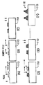
近年、積層回路パターンの作成方法において、光変調素子が利用されており、具体的な作成方法として、まず、図17(A)に示すように、プリント基板の表面を銅メッキした後、図17(B)に示すように、フォトレジストと呼ばれる感光性樹脂を塗布する。
【0003】
このフォトレジストは光が当たると硬化するようになっており(逆の場合もある)、図17(C)に示すように、フォトレジストを光変調素子で露光した後、現像を行うと(図17(D)参照)、露光された部分のフォトレジストが残り、他の部分は洗い流されてしまう。
【0004】
そして、図17(E)に示すように、エッチングにより、フォトレジストが洗い流された部分の銅を腐食させた後、図17(F)に示すように、フォトレジストを剥離して、絶縁材を全面に塗布する(図17(G)参照)。
【0005】
次に、図17(H)に示すように、上下を導通させる必要のある部分をレーザで穴あけした後、図17(I)に示すように、銅メッキをして、フォトレジストを塗布する(図17(J)参照)。
【0006】
そして、図17(K)に示すように、フォトレジストを光変調素子で露光した後、現像を行う(図17(L)参照)。これにより、露光されていない部分のフォトレジストが洗い流され、図17(M)に示すように、エッチングを行って露光されていない部分の銅を腐食させる。
【0007】
次に、図17(N)に示すように、フォトレジストを剥離させた後、図17(O)に示すように、スクリーン印刷により絶縁体を塗布する。ここで、スクリーン印刷には予め穴部が形成されており、この穴部内に半田を付着させ、半田を介して電子部品等を導通させる。
【0008】
ここで、被描画媒体に導電体或いは絶縁体を塗布したり、フォトレジストを露光したりする工程は、それぞれ独立して装置が設けられており、各装置に設けられたステージに被描画媒体をセットして各工程が行われる。このため、各工程毎に被描画媒体をステージにセットしなければならず、作業時間が掛かってしまう。
【0009】
また、各工程毎に装置が独立しているため、各工程毎に被描画媒体の位置決めを行わなければならず、積層されたパターン形成の場合、パターンの位置ズレが生じる場合がある。
【0010】
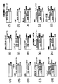
一方、図18(A)、(B)に示すように、3種類の波長露光(例えば、R、G、B)で別の色に発色する銀塩感材を用い、4つの露光ヘッド(R、G、B、UV)を有する露光装置によって、BlackをUV(405nm)、RedをB(450nm)とG(532nm)、GreenをB(450nm)とR(635nm)、BlueをG(532nm)とR(635nm)で露光した後、現像液に通し、現像すると、感材がウエブの場合、同時に全ての色が発色し、各色のパターンが形成されるが、高濃度の着色を得るためには感材の肉厚を数十μmとする必要があり、パターン形成の精度が不充分であった。
【0011】
【発明が解決しようとする課題】
本発明は上記事実を考慮し、簡単な工程で2次元から3次元を含む描画を可能にすると共に、高精度のパターン形成が可能な描画装置及びこの描画装置を用いた描画方法を得ることを目的とする。
【0012】
【課題を解決するための手段】
請求項1に記載の発明では、被描画媒体に対して少なくとも1方向に相対移動し被描画媒体を露光する少なくとも一つの露光ヘッドを設けており、この露光ヘッドの同一の相対移動ラインに沿って又は平行に、被描画媒体に対して少なくとも1方向に相対移動して、機能性材料を吐出する少なくとも一つの吐出ヘッドを設けている。
【0013】
例えば、被描画媒体を載置可能な走査ステージに導電体を吐出する導電吐出ヘッドと、絶縁性樹脂を吐出する絶縁吐出ヘッドと、レーザ光を出射する露光ヘッドと、を互いに平行となるように配設し、同一の移動ラインに沿って移動可能となるようにする。
【0014】
すなわち、同一の走査ステージに各ヘッドを配設する。これにより、走査ステージ上に被描画媒体が載置された状態で、導電吐出ヘッドによって導電体を吐出させて被描画媒体上に導電体層を形成させ、この導電体層以外の部分を絶縁吐出ヘッドによって絶縁性樹脂を吐出させて絶縁体層を形成させた後、加熱機能を有する露光ヘッドによるレーザアニールによって導電体層を硬化させることで、回路パターンを形成させることができる。
【0015】
このように、同一の走査ステージ上で被描画媒体に回路パターンが形成されるようにすることで、被描画媒体に対する各ヘッドの位置ズレが生じないため、パタンの高精度化が容易である。
【0016】
また、同一走査ステージに各ヘッドを配設することで、各ヘッド毎に走査ステージを有する場合と比較して、工程を簡略化することができると共に、パタニング間の時間を短縮することができ、パターン形成の高速化を実現することができる。
【0017】
このため、パタニング間の時間的余裕が取れないメカニズムの場合、例えば、機能性材料を吐出後この機能性材料が変形する前に硬化させなければならない場合でもパターン形成を実施することができると共に、機能性材料が流れる前にこの機能性材料を硬化させることも可能となり、高精度のパターンを形成することができる。また、各走査ステージ間の搬送、或いはパタニング間の移動に要する時間に伴う経時による、パターンの寸法変化の恐れがない。さらに、フォトレジストのように最終的に除去してしまう無駄な材料を必要としないため、コストが削減され、また、フォトレジストを塗布する工程を削減することができるため、工数が低減される。
【0018】
また、同一の走査ステージに各ヘッドを配設することで、各ヘッド毎に走査ステージを有する場合と比較して、回路パターンを形成するために必要な装置全体の設置スペースを小さくすることができ、また、コスト削減及び省電力化を図ることができる。
【0019】
ここで、レーザ露光光源と光変調素子とによる露光ヘッドを用いることで、局所的な加熱が可能となり、サーモバスと異なり被描画媒体の熱伸縮が避けられる。また、局所的に加熱できるため、サーモバスと比較して、被描画媒体の耐熱温度を下げることができる。
【0020】
請求項2に記載の発明では、同一の相対移動ラインに沿って、被描画媒体に対して少なくとも1方向に相対移動し、互いに異なる露光機能を備えた複数の露光ヘッドを設けている。
【0021】
例えば、フォトレジスト用露光ヘッド及びスルーホール用パルスレーザー露光ヘッドを同一の走査ステージに設けることで、フォトレジスト用露光ヘッドによりパターンを形成した後、被描画媒体を移動させることなく、スルーホール用パルスレーザー露光ヘッドによってスルーホールをあけることができるため、穴部の位置合せ精度を向上させることができる。
【0022】
請求項3に記載の発明では、同一の相対移動ラインに沿って、被描画媒体に対して少なくとも1方向に相対移動し、互いに異なる機能性材料を吐出する複数の吐出ヘッドを設けている。
【0023】
請求項4に記載の発明では、被描画媒体を載置する走査ステージを備えており、この走査ステージに、同一の移動ラインに沿って、被描画媒体を露光する露光ヘッド及び前記被描画媒体に機能性材料を吐出する吐出ヘッド、互いに異なる露光機能を備えた複数の露光ヘッド又は、互いに異なる機能性材料を吐出する複数の吐出ヘッド、をそれぞれ配設している。
【0024】
請求項5に記載の発明では、フォトレジストを吐出可能なフォトレジスト吐出ヘッドと、フォトレジストを露光する露光ヘッドと、を被描画媒体の搬送方向に沿って配設しており、フォトレジスト吐出ヘッドによって導電性の被描画媒体にフォトレジストを吐出させた後、このフォトレジストが吐出された領域を露光ヘッドで露光して、被描画媒体上で連続してパターン形成を行う。
【0025】
【発明の実施の形態】
以下、本発明の実施の形態に係る描画装置について説明する。
【0026】
図1に示すように、描画装置10には略直方体状の走査ステージ12が備えられており、走査ステージ12の上面には、被描画媒体としてのプリント基板14が位置決めされた状態で載置可能となっている。また、描画装置10には、走査ステージ12の長手方向に沿った端部に、略直方体状のヘッド保持体16が備えられている。
【0027】
このヘッド保持体16には、図2に示すように、ヘッド保持体16の長手方向に沿ってガイドレール18が配設されており、露光ヘッド20及び吐出ヘッド22(図1で示す吐出ヘッド24については、吐出ヘッド22と構成が略同一であるため、図示及び説明を省略する)が、連結部26、28を介して、ヘッド保持体16の長手方向に対して直交した状態でそれぞれ片持ち支持され、ガイドレール18に沿ってそれぞれ矢印A方向を移動可能となっている(以下、この矢印A方向を「主走査方向」という)。
【0028】
露光ヘッド20及び吐出ヘッド22の連結部26、28は、リニアモータ(図示省略)となっており、図示しない駆動装置によってリニアモータが駆動することで、露光ヘッド20及び吐出ヘッド22が、連結部26、28を介してガイドレール18に沿って移動する。
【0029】
一方、図1に示すように、この描画装置10の制御部は、CPU(中央演算処理装置)30を具備しており、図示しない入力装置からの作業命令がCPU30に入力されると、露光ヘッド20の走査速度等の作業条件に対応してレーザエネルギのレベル等の制御内容を決定するため、CPU30に接続されたメモリに格納されている記録条件とヘッド送り速度との関係を記録したテーブル32から、作業条件に適合したレーザエネルギのレベル等の設定値を読み取る。
【0030】
テーブル32から読み取ったレーザエネルギのレベル等の設定値に基づいて露光ヘッド20を制御するための制御信号を記録条件設定回路34へ送信する。この記録条件設定回路34は、レーザエネルギに関する設定値を含めた制御信号を記録レーザドライバ36へ送信し、記録レーザドライバ36を介して、露光ヘッド20のファイバアレイ光源66(図4(A)、(B)参照)を駆動させることで、レーザ光が発光可能となる。
【0031】
また、CPU30は、テーブル32から読み取ったレーザエネルギのレベル等の設定値に基づいて露光ヘッド20を制御するための制御信号を露光ヘッド20用の主走査ドライバ38へ送信する。この露光ヘッド20用の主走査ドライバ38は、ヘッド保持体16に設けられた駆動装置へ露光ヘッド20を移動操作させる制御信号を送信して露光ヘッド20を主走査方向へ移動させる。
【0032】
また、露光ヘッド20用の主走査ドライバ38は、制御信号を記録同期信号発生回路40へ送り、露光ヘッド20の移動速度に対応して露光ヘッド20の露光タイミングを同期させるべく、記録同期信号発生回路40を介して変調素子ドライバ42へ同期信号を送信する。
【0033】
この変調素子ドライバ42では、CPU30のメモリに記憶している記録データ44から、描画パターンの記録情報を読み出して、この描画パターンの記録情報に基づいて、プリント基板14が露光される。
【0034】
さらに、CPU30は、テーブル32から読み取ったレーザエネルギのレベル等の設定値に基づいて吐出ヘッド22を制御するための制御信号を吐出ヘッド22用の主走査ドライバ48へ送信する。
【0035】
この吐出ヘッド22用の主走査ドライバ48は、吐出ヘッド22を移動させる駆動装置へ制御信号を送信し、吐出ヘッド22を主走査方向へ移動させると共に、図示しない同期信号発生回路によって、吐出ヘッド22の移動速度に対応して吐出ヘッド22に封入された機能性材料の吐出タイミングを同期させるべく、吐出素子ドライバ50へ同期信号を送信し、静電方式等による吐出手段によって、記録された描画パターンの記録情報に基づき、プリント基板14に機能性材料を吐出させる。
【0036】
また、CPU30は、テーブル32から読み取ったレーザエネルギのレベル等の設定値に基づいて吐出ヘッド24を制御するための制御信号を吐出ヘッド24用の主走査ドライバ52を介して、吐出ヘッド24を移動させる駆動装置へ制御信号を送信し、吐出ヘッド24を主走査方向へ移動させると共に、図示しない同期信号発生回路を介して吐出素子ドライバ54へ同期信号を送信し、静電方式等による吐出手段によって、記録された描画パターンの記録情報に基づき、プリント基板14に機能性材料を吐出させる。
【0037】
一方、図2に示すように、露光ヘッド20及び吐出ヘッド22、24をガイドレール18に沿って移動可能に連結させる連結部26、28には、それぞれネジ部(図示省略)を設けており、矢印A方向及び矢印A方向に対して直交する矢印B方向に対して、ガイドレール18に対する連結部26、28の位置調整ができるようにしている。
【0038】
これにより、露光ヘッド20及び吐出ヘッド22、24の矢印A方向及び矢印B方向に対する位置調整が可能となる。具体的には、露光ヘッド20及び吐出ヘッド22、24によって、規定パターンをプリント基板14上にパタニングし、目標パターンと実際のパターンの差を測定して、位置調整を行う。
【0039】
例えば、吐出ヘッド22の3本目の吐出ラインが露光ヘッド20の露光ラインと一致するパターンを目標パターンとし、露光ラインが吐出ラインの何本目に一致しているかを見て、露光ヘッド20の位置調整を行う。逆に、露光ラインを基準として吐出ヘッド22の位置調整を行っても良い。
【0040】
なお、ここでは、連結部26、28に設けたネジ部によって露光ヘッド20及び吐出ヘッド22、24の位置調整が可能となるようにしたが、露光ヘッド20に用いられる変調素子或いは吐出ヘッド22、24に用いられる吐出素子の配列データを図示しない制御部に送信して露光ヘッド20及び吐出ヘッド22、24を自動的に位置調整できるようにしても良い。
【0041】
この場合、矢印A方向に関しては、同期信号発生回路による露光或いは吐出タイミングの調整によって露光ライン及び吐出ラインの矢印A方向の位置調整を図ることもできる。
【0042】
ところで、吐出ヘッド22、24はインクジェット方式で構成されており、吐出ヘッド22には、加熱によって導電性発現する、導電体としての銅微粒子樹脂カプセル分散液が封入され、吐出ヘッド24には絶縁体としての絶縁性樹脂分散液が封入されている。また、吐出ヘッド22、24はそれぞれ静電方式で構成されており、静電気力によって封入された機能性材料を外部へ吐出させる。
【0043】
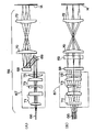
一方、露光ヘッド20は、図3及び図4(A)、(B)に示すように、複数の照射ヘッド56によって構成されており、各照射ヘッド56には、ファイバアレイ光源66が備えられ、光源波長は350〜450nmである(但し、ヒートモードの場合は、波長範囲が広がり350〜950nmとなる)。
【0044】
このファイバアレイ光源66から出射されたレーザ光は、レンズ系67を構成する1対の組合せレンズ71によって平行光化され、1対の組合せレンズ73へ入射される。この組合せレンズ73は、レーザ出射端の配列方向に対しては、レンズの光軸に近い部分は光束を広げ且つ光軸から離れた部分は光束を縮め、配列方向と直交する方向に対しては光をそのまま通過させる機能を備えており、光量分布が均一となるようにレーザ光を補正する。
【0045】
この組合せレンズ73によって、光量分布が均一となるように補正されたレーザ光は、集光レンズ75によって集光され、反射ミラー69を介して、入射された光ビームを画像データに応じて各画素毎に変調する空間光変調素子としてのデジタル・マイクロミラー・デバイス68(以下、「DMD68」という)へ入射される。
【0046】
DMD68へ入射されたレーザ光は、レンズ系70、72によりプリント基板14上に結像される。ここで、DMD68は、図5に示すように、SRAMセル(メモリセル)60上に、微小ミラー(マイクロミラー)62が支柱により支持されて配置されたものであり、画素(ピクセル)を構成する多数の(例えば、600個×800個)の微小ミラーを格子状に配列して構成されたミラーデバイスである。
【0047】
各ピクセルには、最上部に支柱に支えられたマイクロミラー76が設けられており、マイクロミラー76の表面にはアルミニウム等の反射率の高い材料が蒸着され、マイクロミラー76の反射率は90%以上である。
【0048】
また、マイクロミラー76の直下には、ヒンジ及びヨークを含む支柱を介して通常の半導体メモリの製造ラインで製造されるシリコンゲートのCMOSのSRAMセル74が配置されており、全体はモノリシック(一体型)に構成されている。
【0049】
DMD68のSRAMセル74にデジタル信号が書き込まれると、支柱に支えられたマイクロミラー76が、対角線を中心としてDMD68が配置された基板側に対して±α度(例えば±10度)の範囲で傾けられる。
【0050】
ここで、図6(A)は、マイクロミラー76がオン状態である+α度に傾いた状態を示し、図6(B)は、マイクロミラー76がオフ状態である−α度に傾いた状態を示しており、画像信号に応じて、DMD68の各ピクセルにおけるマイクロミラー76の傾きを制御することによって、DMD68に入射された光はそれぞれのマイクロミラー76の傾き方向へ反射される。
【0051】
また、図5は、DMD68の一部を拡大し、マイクロミラー76が+α度又は−α度に制御されている状態の一例を示しており、それぞれのマイクロミラー76のオンオフ制御は、DMD68に接続された図示しないコントローラによって行われる。なお、オフ状態のマイクロミラー76により光ビームが反射される方向には、光吸収体(図示せず)が配置されている。
【0052】
また、DMD68は、図7に示すように、マイクロミラー76が多数個(例えば、800列×600行)配列されているが、千鳥状に配置すると共に、主走査方向(矢印A方向)に対して所定角度(例えば、0.1°〜5°)を成すように僅かに傾斜させ、露光ヘッド20を主走査させたときに、隣接する露光部分が若干重なり合うようにしている。
【0053】
これにより、DMD68の位置が多少ズレたとしても該ズレを吸収することができ、高精細な露光を実現することができると共に、重なり合う部分のマイクロミラー76のうちどちらか一方を、オフ状態とすることで、多重露光を回避することもできる。
【0054】
次に、本発明の実施の形態に係る描画装置の作用について説明する。
【0055】
図8(A)に示すように、記録された描画パターンの記録情報に基づき、絶縁体吐出ヘッド24(図1参照)によって、走査ステージ12(図1参照)の上面に位置決めされたプリント基板14上に絶縁性樹脂分散液80を吐出させる。
【0056】
次に、加熱によって導電性発現する導電体が封入された導電体吐出ヘッド22(図1参照)によって、図8(B)に示すように、記録された描画パターンの記録情報に基づき、導電体としての銅微粒子樹脂カプセル分散液82を吐出させる(なお、プリント基板14上に銅微粒子樹脂カプセル分散液82を吐出させた後に絶縁性樹脂分散液80を吐出させても良い)。
【0057】
そして、加熱機能を有する露光ヘッド20(図1参照)によって、図8(C)に示すように、プリント基板14を全面露光し、銅微粒子樹脂カプセル分散液82及び絶縁性樹脂分散液80を硬化させる。
【0058】
ここで、絶縁性樹脂分散液の種類によっては、露光ヘッド20を構成するDMD68(図5参照)のマイクロミラー76(図5参照)を制御して銅微粒子樹脂カプセル分散液82が吐出された領域のみ露光させることもできる(なお、必要な領域のみを局所的に露光できるということであり、銅微粒子樹脂カプセル分散液82が吐出された領域より少し広い領域を露光しても良い)。
【0059】
この場合、プリント基板14を局所的に露光することができ、サーモアニールによる場合と異なり表面だけ加熱されるため、プリント基板14の熱伸縮が避けられ、また、プリント基板14の耐熱温度を下げることができる。また、サーモアニールによる場合と比較して時間の削減を図ることができる。
【0060】
さらに、サーモアニールでは、銅微粒子樹脂カプセル分散液82中の樹脂が完全に蒸散せず、また銅微粒子間に間隙が残るため、抵抗値が十分下がりきらない問題がある(抵抗値:5〜8×10⁻⁵Ωcm)が、レーザアニールによる場合は、通常のメッキによる銅配線パタン同等の抵抗値(3〜5×10⁻⁶Ωcm)となるため、一般的な回路基板の用途に広く用いることができる。
【0061】
次に、図8(D)に示すように、銅微粒子樹脂カプセル分散液82及び絶縁性樹脂分散液80が硬化して形成された絶縁性層84及び銅微粒子層86の上に、絶縁体吐出ヘッド24によって、絶縁性樹脂分散液80を吐出させ、導電体吐出ヘッド22によって、銅微粒子樹脂カプセル分散液82を吐出させた後、図8(E)に示すように、露光ヘッド20によって、プリント基板14を全面露光して、銅微粒子樹脂カプセル分散液82及び絶縁性樹脂分散液80を硬化させる。
【0062】
そして、図8(F)に示すように、絶縁性層84及び銅微粒子層86上に、絶縁体吐出ヘッド24によって、絶縁性樹脂分散液80を吐出させ、導電体吐出ヘッド22によって、銅微粒子樹脂カプセル分散液82を吐出させた後、図8(G)に示すように、露光ヘッド20によって、プリント基板14を全面露光して、銅微粒子樹脂カプセル分散液82及び絶縁性樹脂分散液80を硬化させる。
【0063】
次に、図8(H)に示すように、絶縁性層84及び銅微粒子層86上に、半田を付けて外の回路基板から電極を取り出す領域を除いて、絶縁体吐出ヘッド24によって、絶縁性樹脂分散液80を吐出させ、プリント基板14の表面を絶縁性樹脂によって被覆する。
【0064】
このように、加熱によって導電性発現する材料を吐出ヘッド22でプリント基板14上に吐出(プリント基板14の全面に吐出させたいわゆる塗布状態としても良い)させた後、加熱機能を有する露光ヘッドによってアニーリング(全面或いは局所)することで、簡単に導電性のパタニングを行うことができ、積層回路基板88を簡単に形成させることができる。
【0065】
本形態では、図1に示すように、同一の走査ステージ12に露光ヘッド20及び吐出ヘッド22、24を配設することで、各ヘッド毎に走査ステージを有する場合と比較して、工程を簡略化することができると共に、パタニング間の時間を短縮することができ、パターン形成の高速化を実現することができる。
【0066】
また、同一の走査ステージ12でプリント基板14に回路パターンが形成されるようにすることで、プリント基板14に対する露光ヘッド20及び吐出ヘッド22、24の位置ズレが生じないため、パターンの高密度化が容易である。
【0067】
このため、パタニング間の時間的余裕が取れないメカニズムの場合、例えば、絶縁体或いは導電体などの機能性材料を吐出後この機能性材料が変形する前に硬化させなければならない場合でもパターン形成を実施させることができると共に、機能性材料が流れる前にこの機能性材料を硬化させることも可能となり、高精度のパターンが形成される。
【0068】
また、各走査ステージ12間の搬送、或いはパタニング間の移動に要する時間に伴う経時による、パターンの寸法変化の恐れがない。さらに、フォトレジストのように最終的に除去してしまう無駄な材料を必要としないため、コストが削減され、また、フォトレジストを塗布する工程を削減することができるため、工数が低減される。
【0069】
また、同一の走査ステージに露光ヘッド20及び吐出ヘッド22、24を配設することで、各ヘッド毎に走査ステージを有する場合と比較して、回路パターンを形成するために必要な装置全体の設置スペースを小さくすることができ、また、コスト削減及び省電力化を図ることができる。
【0070】
なお、本形態では、走査ステージ12に、光変調器としてDMDを用いたアニール用の露光ヘッド20、銅微粒子樹脂カプセル分散液82を吐出させる静電方式の吐出ヘッド22及び絶縁性樹脂分散液80を吐出させる静電方式の吐出ヘッド24を設ける等したが、本発明はこの実施例に限るものではない。
【0071】
例えば、露光ヘッドの光変調器として、DMDを備えた照射ヘッドについて説明したが、例えば、MEMS(Micro Electro Mechanical Systems)タイプの空間変調素子(SLM;Spacial Light Modulator)や、電気光学効果により透過光を変調する光学素子(PLZT素子)や液晶光シャッタ(FLC)等、MEMSタイプ以外の空間変調素子を用いた場合にも、基板上に配列された全画素部に対し一部の画素部を使用することで、1画素当り、1主走査ライン当たりの変調速度を速くすることができるので、同様の効果を得ることができる。
【0072】
なお、MEMSとは、IC製造プロセスを基盤としたマイクロマシニング技術によるマイクロサイズのセンサ、アクチュエータ、そして制御回路を集積化した微細システムの総称であり、MEMSタイプの空間変調素子とは、静電気力を利用した電気機械動作により駆動される空間変調素子を意味している。
【0073】
また、感光性材料としては、フォトレジスト、ジアゾ、フォトポリマー、微粒子分散材料(樹脂、誘電体、導電材、それらのカプセル構造粒子)、熱結晶化材料、感熱材料、熱転写材料、分子拡散材料(いわゆる昇華型熱転写材料)等があり、感光性材料形態は、フィルム、液状、固体、微粒子、微粒子分散液、微粒子成膜フィルム(基板)等があるが、露光ヘッドにより、2次元描画として、いわゆるパタニング(エッチングマスク、メッキマスク、撥水親水、凹凸、熱アニール、熱転写、熱反応、アブレーション等)を形成し、3次元描画(2次元描画を複数回繰り返すもの)として、光硬化、粉末焼結、熱溶融、熱硬化による立体造形を形成することができれば良い。
【0074】
一方、吐出ヘッドを構成するインクジェットヘッドには、オンデマンドノズルタイプ(ピエゾ、静電メンブレム、サーマル等)、コンティニュアスタイプ(電界偏向、熱偏向等)又は、オンデマンドノズルレスタイプ(超音波、静電吐出等)があり、吐出材料としては、光反応液、微粒子分散液(樹脂、誘電体、導電材、熱結晶化材料、感熱材料、熱溶融材料、分子拡散材料(いわゆる昇華型熱転写材料)、触媒、酵素、バクテリア、DNA、化学反応薬品等と、それらのカプセル構造粒子)、熱溶融液(WAX等)、化学反応液、触媒溶液、表面改質液等がある。
【0075】
この吐出ヘッドにより、2次元描画として、パタニング(エッチングマスク、メッキマスク、撥水親水、凹凸)を形成し、3次元描画として、熱溶融冷却硬化、光硬化、粉末焼結、熱硬化による立体造形を形成することができれば良い。
【0076】
具体的には、導電性微粒子含有液吐出ヘッド及び露光へッドを用いても良い。図9(A)に示すように、ガラス基板90上に導電性微粒子含有液吐出ヘッドによって、導電性微粒子を含む液92を全面吐出させる。次に、図9(B)に示すように、露光ヘッドによって、導電性微粒子を含む液が塗布された絶縁材を、必要な導電パターン状にアニールすることで、導電膜のパターン96が形成され、回路基板98が形成される。
【0077】
ここで、上記導電性微粒子としては、銅、銀、金等の10nm〜10μmの微粒子の周りを絶縁体で被覆したものを用いることができる。
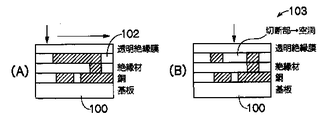
【0078】
また、絶縁膜吐出ヘッド及び回路切断パルスレーザー露光ヘッドを用いても良い。図10(A)に示すように、絶縁膜吐出ヘッドによってプリント基板100の最外層の導電膜102に透明絶縁膜を全面吐出させる。この透明絶縁膜を、透明絶縁膜は透過するが、導電膜吐出ヘッド或いはメッキで形成された導電膜は吸収する波長を備えた露光ヘッドによって露光することで、図10(B)に示すように、導電膜102の回路パターンを切断して空洞とする回路基板103が形成される。
【0079】
この回路基板103では、表面にでていない回路パターンの変更が可能となり、回路パターンが空気に触れない状態で加熱できるため、切断部周辺の導電膜材料が酸化しにくい。
【0080】
さらに、絶縁膜吐出ヘッド、マーキングインキ吐出ヘッドまたはパルスレーザーマーキング露光ヘッドを用いて、最外層の絶縁膜をつける前に、露光ヘッドまたは吐出ヘッドで番号、バーコード、位置あわせマーク等のマーキングを行っても良い。
【0081】
最外層の絶縁膜をつける前にマーキングが為されるため、マークは表面に直接露出することはなく、偽造や剥離を防止することができる。また、各層毎に異なる内容でマーキングすることができるため、回路が各層毎で異なる場合の検査条件の間違い防止にもなり、最終製品に回路基板が実装される場合の実装間違いも防ぐことができる。
【0082】
また、スペーサー構造材料吐出ヘッド及び硬化用レーザー露光ヘッドを用いても良い。図11(A)に示すように、スペーサー構造材料吐出ヘッドによって、LCD104のガラス間隔を均一にするためのスペーサー106を吐出させた後、露光ヘッド(材料が光硬化型なら350〜450nmの紫外レーザー、材料が熱硬化型の場合、350〜950nmのハイパワーレーザーを光源とする)によって、図11(B)に示すように、スペーサー106該当位置周辺のみ照射してスペーサー106を硬化させることで、基板105が形成される。
【0083】
この基板105では、スペーサー106の高さ精度が向上すると共に、スペーサー106を高強度化することができる。また、これにより、ウエハレベルフリップチップのバンプ用のスペーサとしても応用可能となる。
【0084】
さらに、フォトポリマ吐出ヘッド及び硬化用露光ヘッドを用いても良い。図12(A)に示すように、昇降可能に設けられた台110の上面にフォトポリマ吐出ヘッドによって、フォトポリマを1層分パターン状に吐出させる。次に、図12(B)に示すように、露光ヘッドによって、350〜450nmの光を照射してフォトポリマを硬化させ、図12(C)に示すように、台110を下降(約50μm)させて、フォトポリマ吐出ヘッド及び硬化用露光ヘッドを相対的に1層分上昇させる。このとき、露光ヘッド及びフォトポリマ吐出ヘッドを基準位置に戻す。
【0085】
そして、図12(D)に示すように、フォトポリマ吐出ヘッドによって、フォトポリマを1層分パターン状に吐出させた後、露光ヘッドによって、フォトポリマを硬化させ、図12(E)に示すように、台110を下降させて、フォトポリマ吐出ヘッド及び硬化用露光ヘッドを相対的に1層分上昇させる。以上のような工程を複数回繰り返すことで、図12(F)に示すように、回路基板112が形成され、光で固めないものに比べ高強度、高精度の立体造形を行うことができる。
【0086】
また、導電吐出ヘッド及びトリミング用パルスレーザー露光ヘッドを用いても良い。図13(A)に示すように、導電吐出ヘッドによってプリント基板113上に導電回路(導電体)を形成した後、図13(B)に示すように、抵抗計114により、抵抗値を測定しながら、露光ヘッド(パルスレーザーが望ましい)によって導電回路を削り(一般にトリミングと呼ぶ)、目標抵抗値になったら照射を停止する。
【0087】
そして、図13(C)に示すように、プリント基板113の上面を絶縁体によって被覆することで、回路基板115が形成される。このような工程により、回路基板に高精度の抵抗を作ることが可能になると共に、多数の抵抗を一度に調整することが可能となる。
【0088】
さらに、互いに異なる露光機能を有するフォトレジスト用露光ヘッドとスルーホール用パルスレーザー露光ヘッドとを用いても良い。図14(A)に示すように、銅メッキされた銅メッキ基板116に、図14(B)に示すように、パルスレーザー搭載のスルーホール用パルスレーザ露光ヘッドによってスルーホール118をあける。
【0089】
そして、図14(C)に示すように、銅メッキ基板116の両面をフィルム上のフォトレジストでラミネートし、図14(D)に示すように、フォトレジスト用露光ヘッドにより、フォトレジストを硬化させた後、図14(E)に示すように、現像によって未露光部のフォトレジストを取り除き(なお、ここでは、露光によって、現像液に対して不溶性となる、いわゆるネガ型フォトレジストを用いたが、露光によって現像液に溶解し易くなる、いわゆるポジ型フォトレジストを用いても良く、ポジ型フォトレジストを用いた場合、現像によって露光部のフォトレジストが取り除かれる)、フォトレジストが取り除かれ露出した銅をエッチングによって腐食させる。
【0090】
次に、図14(F)に示すように、フォトレジストを剥離する。次に、図14(G)に示すように、銅メッキ基板116の両面をフィルム上のフォトレジストでラミネートし、図14(H)に示すように、フォトレジスト用露光ヘッドにより、フォトレジストを硬化させた後、図14(I)に示すように、現像によって未露光部のフォトレジストを取り除く。
【0091】
そして、図14(J)に示すように、銅メッキ基板116に形成されたスルーホール118の内縁部をメッキした後、図14(K)に示すように、フォトレジストを剥離して、回路基板120を形成する。このように、同一装置でスルーホールを開けることで、穴部の位置合せ精度を向上させることができる。
【0092】
なお、以上の形態では、走査ステージにプリント基板を載置させた状態でパターンが形成される方法について説明したが、各ヘッドを固定し、被描画媒体を移動させてパターンを形成させても良い。
【0093】
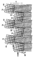
図15に示すように、被描画媒体として長尺状のウエブ122を用いる。送出装置124によって送出されたウエブ122は、巻取装置126によって巻き取られるようになっており、送出装置124と巻取装置126との間で搬送路128が構成される。
【0094】
この搬送路128には、搬送されるウエブ122を間に置いて上下に、フォトレジストを吐出するフォトレジスト吐出ヘッド130、露光ヘッド132、現像液を吐出する現像液吐出ヘッド134、エッチング液を吐出するエッチング液吐出ヘッド138及び洗浄液を吐出する洗浄液吐出ヘッド140を、それぞれ搬送路128に対して直交する方向に配設しており、隣接するヘッド同士が互いに平行となるように配置されている。
【0095】
これにより、ウエブ122が搬送さる過程で、ウエブ122の移動と共に各処理が施されて、パターンが形成される。なお、ここでは、搬送されるウエブ122の上下に各ヘッドを配置したが、ウエブ122の上方或いは下方のみでも良い。また、ここでは、現像液吐出ヘッド134、エッチング液吐出ヘッド138及び洗浄液吐出ヘッド140を用いたが、必ずしも吐出ヘッドを用いる必要はなく、現像液、エッチング液、洗浄液がそれぞれ貯留されたタンクを用いても良い。
【0096】
また、ヘッドの形態の組み合わせとして、図1に示すように、露光ヘッド20及び吐出ヘッド22、24がラインヘッドである場合について説明したが、これに限るものではなく、例えば、図16に示すように、露光ヘッド142及び吐出ヘッド144、146がシリアルヘッドであっても良く(この場合、主走査方向(矢印A方向)と直交する方向に対しても移動可能とする)、また、図示はしないが、吐出ヘッドがシリアルヘッドで露光ヘッドがラインヘッドである場合、吐出ヘッドがラインヘッドで露光ヘッドがポリゴン走査ヘッドである場合、吐出ヘッドがラインヘッドで露光ヘッドがシリアルヘッドである場合等、様々な組み合わせが可能である。
【0097】
【発明の効果】
本発明は、上記構成としたので、同一の走査ステージ上で被描画媒体に回路パターンが形成されるようにすることで、被描画媒体に対する各ヘッドの位置ズレが生じないため、パタンの高精度化が容易である。
【0098】
また、同一走査ステージに各ヘッドを配設することで、各ヘッド毎に走査ステージを有する場合と比較して、工程を簡略化することができると共に、パタニング間の時間を短縮することができ、パターン形成の高速化を実現することができる。このため、高精度のパターンを形成することができ、また、各走査ステージ間の搬送、或いはパタニング間の移動に要する時間に伴う経時による、パターンの寸法変化の恐れがない。
【0099】
また、フォトレジストのように最終的に除去してしまう無駄な材料を必要としないため、コストが削減され、また、フォトレジストを塗布する工程を削減することができるため、工数が低減される。
【0100】
さらに、同一の走査ステージに各ヘッドを配設することで、各ヘッド毎に走査ステージを有する場合と比較して、回路パターンを形成するために必要な装置全体の設置スペースを小さくすることができ、また、コスト削減及び省電力化を図ることができる。
【図面の簡単な説明】
【図1】本発明の実施形態に係る描画装置を示す斜視図及び描画装置の動作を示すブロック図である。
【図2】本発明の実施形態に係る描画装置に備えられた露光ヘッド及び吐出ヘッドの位置調整方法を示す説明図である。
【図3】本発明の実施形態に係る描画装置に備えられた露光ヘッドの照射ヘッドの概略構成を示す斜視図である。
【図4】(A)は図3に示す照射ヘッドの構成を示す光軸に沿った副走査方向の断面図であり、(B)は(A)の側面図である。
【図5】本発明の実施形態に係る描画装置に備えられた露光ヘッドを構成するDMDの構成を示す部分拡大図である。
【図6】(A)及び(B)はDMDの動作を説明するための説明図である。
【図7】本発明の実施形態に係る描画装置に備えられた露光ヘッドのレーザ光の走査線を示す平面図である。
【図8】(A)〜(H)は、本発明の実施形態に係る描画装置に備えられた露光ヘッド及び吐出ヘッドによって回路基板を形成する方法を示す断面図である。
【図9】(A)及び(B)は、本発明の実施形態に係る描画装置の変形例としての露光ヘッド及び吐出ヘッドによって回路基板を形成する方法を示す断面図である。
【図10】(A)及び(B)は、本発明の実施形態に係る描画装置の変形例としての露光ヘッド及び吐出ヘッドによって回路基板を形成する方法を示す断面図である。
【図11】(A)及び(B)は、本発明の実施形態に係る描画装置の変形例としての露光ヘッド及び吐出ヘッドによって回路基板を形成する方法を示す断面図である。
【図12】(A)〜(F)は、本発明の実施形態に係る描画装置の変形例としての露光ヘッド及び吐出ヘッドによって回路基板を形成する方法を示す断面図である。
【図13】(A)〜(C)は、本発明の実施形態に係る描画装置の変形例としての露光ヘッド及び吐出ヘッドによって回路基板を形成する方法を示す断面図である。
【図14】(A)〜(K)は、本発明の実施形態に係る描画装置の変形例としての露光ヘッド及び吐出ヘッドによって回路基板を形成する方法を示す断面図である。
【図15】本発明の実施形態に係る描画装置の変形例を示す説明図である。
【図16】本発明の実施形態に係る描画装置の他の変形例を示す斜視図及び描画装置の動作を説明するブロック図である。
【図17】(A)〜(O)は、従来の回路基板を形成する方法を示す断面図である。
【図18】(A)及び(B)は、複数の露光ヘッドでパターンを形成する方法を示す断面図である。
【符号の説明】
10 描画装置
12 走査ステージ
20 露光ヘッド
22 導電体吐出ヘッド(吐出ヘッド)
24 絶縁体吐出ヘッド(吐出ヘッド)
130 フォトレジスト吐出ヘッド
132 露光ヘッド
142 露光ヘッド
144 吐出ヘッド
146 吐出ヘッド[0001]
BACKGROUND OF THE INVENTION
The present invention relates to a drawing apparatus for drawing a laminated circuit pattern and the like, and a drawing method using the drawing apparatus.
[0002]
[Prior art]
In recent years, a light modulation element has been used in a method for producing a laminated circuit pattern. As a specific production method, first, as shown in FIG. As shown in (B), a photosensitive resin called a photoresist is applied.
[0003]
This photoresist is cured when exposed to light (and vice versa). As shown in FIG. 17C, when the photoresist is exposed to a light modulation element and then developed (FIG. 17 (D)), the exposed portion of the photoresist remains, and the other portions are washed away.
[0004]
Then, as shown in FIG. 17E, after etching, the copper in the portion where the photoresist has been washed away is corroded, and then the photoresist is peeled off as shown in FIG. Application is performed on the entire surface (see FIG. 17G).
[0005]
Next, as shown in FIG. 17 (H), a portion that needs to be conducted vertically is drilled with a laser, and then copper plating is applied as shown in FIG. 17 (I) to apply a photoresist ( (See FIG. 17 (J)).
[0006]
Then, as shown in FIG. 17K, the photoresist is exposed with a light modulation element and then developed (see FIG. 17L). As a result, the unexposed portions of the photoresist are washed away, and as shown in FIG. 17M, etching is performed to corrode the unexposed portions of copper.
[0007]
Next, as shown in FIG. 17N, after the photoresist is peeled off, an insulator is applied by screen printing as shown in FIG. Here, a hole is formed in advance in the screen printing, and solder is attached to the hole, and an electronic component or the like is conducted through the solder.
[0008]
Here, the process of applying a conductor or insulator to the drawing medium or exposing the photoresist is provided with an apparatus independently, and the drawing medium is placed on a stage provided in each apparatus. Each process is performed by setting. For this reason, it is necessary to set the drawing medium on the stage for each process, which takes work time.
[0009]
In addition, since the apparatus is independent for each process, the drawing medium must be positioned for each process. In the case of stacked pattern formation, pattern misalignment may occur.
[0010]
On the other hand, as shown in FIGS. 18A and 18B, four exposure heads (R) using a silver salt sensitive material that develops different colors in three types of wavelength exposure (for example, R, G, B) are used. , G, B, UV), Black is UV (405 nm), Red is B (450 nm) and G (532 nm), Green is B (450 nm) and R (635 nm), Blue is G (532 nm) When the photosensitive material is a web, all colors are developed at the same time, and a pattern of each color is formed. However, in order to obtain a high density coloring However, the thickness of the light-sensitive material needs to be several tens of μm, and the pattern formation accuracy is insufficient.
[0011]
[Problems to be solved by the invention]
In consideration of the above facts, the present invention enables drawing including 2D to 3D in a simple process and obtains a drawing apparatus capable of forming a highly accurate pattern and a drawing method using the drawing apparatus. Objective.
[0012]
[Means for Solving the Problems]
According to the first aspect of the present invention, there is provided at least one exposure head that relatively moves in at least one direction with respect to the drawing medium and exposes the drawing medium, and follows the same relative movement line of the exposure head. Alternatively, in parallel, at least one ejection head that ejects the functional material by moving relative to the drawing medium in at least one direction is provided.
[0013]
For example, a conductive discharge head that discharges a conductor to a scanning stage on which a drawing medium can be placed, an insulating discharge head that discharges an insulating resin, and an exposure head that emits laser light are parallel to each other. It is arranged so that it can move along the same movement line.
[0014]
That is, each head is disposed on the same scanning stage. As a result, in a state where the drawing medium is placed on the scanning stage, the conductive discharge head discharges the conductor to form a conductive layer on the drawing medium, and the portions other than the conductive layer are insulated and discharged. After the insulating resin is discharged by the head to form the insulator layer, the circuit pattern can be formed by curing the conductor layer by laser annealing with an exposure head having a heating function.
[0015]
As described above, since the circuit pattern is formed on the drawing medium on the same scanning stage, the positional deviation of each head with respect to the drawing medium does not occur, so that it is easy to improve the pattern accuracy.
[0016]
Also, by arranging each head on the same scanning stage, the process can be simplified and the time between patterning can be shortened as compared with the case where each head has a scanning stage. High speed pattern formation can be realized.
[0017]
For this reason, in the case of a mechanism that does not allow time between patterning, for example, pattern formation can be performed even if the functional material has to be cured after being discharged before the functional material is deformed, This functional material can be cured before the functional material flows, and a highly accurate pattern can be formed. In addition, there is no fear of pattern dimensional changes due to aging with the time required for conveyance between scanning stages or movement between patterns. Furthermore, since unnecessary materials that are finally removed like a photoresist are not required, the cost is reduced, and the number of steps can be reduced because the step of applying the photoresist can be reduced.
[0018]
Also, by arranging each head on the same scanning stage, the installation space of the entire apparatus necessary for forming the circuit pattern can be reduced as compared with the case where each head has a scanning stage. In addition, cost reduction and power saving can be achieved.
[0019]
Here, by using an exposure head composed of a laser exposure light source and a light modulation element, local heating is possible, and unlike the thermobus, thermal expansion and contraction of the drawing medium can be avoided. Moreover, since it can heat locally, the heat-resistant temperature of a drawing medium can be lowered | hung compared with a thermo bath.
[0020]
According to the second aspect of the present invention, a plurality of exposure heads that are relatively moved in at least one direction with respect to the drawing medium along the same relative movement line and that have different exposure functions are provided.
[0021]
For example, by providing a photoresist exposure head and a through-hole pulse laser exposure head on the same scanning stage, a pattern is formed by the photoresist exposure head, and then the through-hole pulse is moved without moving the drawing medium. Since the through hole can be formed by the laser exposure head, the alignment accuracy of the hole can be improved.
[0022]
According to a third aspect of the present invention, there are provided a plurality of ejection heads that relatively move in at least one direction with respect to the drawing medium along the same relative movement line and eject different functional materials.
[0023]
According to a fourth aspect of the present invention, a scanning stage on which a drawing medium is placed is provided, and an exposure head that exposes the drawing medium along the same movement line on the scanning stage and the drawing medium. A discharge head for discharging a functional material, a plurality of exposure heads having different exposure functions, or a plurality of discharge heads for discharging different functional materials are provided.
[0024]
In the invention according to claim 5, a photoresist discharge head capable of discharging a photoresist and an exposure head for exposing the photoresist are arranged along the transport direction of the drawing medium, and the photoresist discharge head After discharging the photoresist onto the conductive drawing medium, the region where the photoresist is discharged is exposed by the exposure head, and the pattern is continuously formed on the drawing medium.
[0025]
DETAILED DESCRIPTION OF THE INVENTION
Hereinafter, a drawing apparatus according to an embodiment of the present invention will be described.
[0026]
As shown in FIG. 1, the
[0027]
As shown in FIG. 2, a
[0028]
The connecting
[0029]
On the other hand, as shown in FIG. 1, the control unit of the
[0030]
A control signal for controlling the
[0031]
Further, the
[0032]
The
[0033]
In the
[0034]
Further, the
[0035]
The
[0036]
Further, the
[0037]
On the other hand, as shown in FIG. 2, the connecting
[0038]
Thereby, the position adjustment of the
[0039]
For example, the pattern in which the third discharge line of the
[0040]
Here, the positions of the
[0041]
In this case, with respect to the direction of the arrow A, it is possible to adjust the position of the exposure line and the discharge line in the direction of the arrow A by adjusting the exposure or discharge timing by the synchronization signal generation circuit.
[0042]
By the way, the discharge heads 22 and 24 are configured by an ink jet system, and the
[0043]
On the other hand, as shown in FIGS. 3 and 4A and 4B, the
[0044]
The laser light emitted from the fiber array light source 66 is collimated by a pair of
[0045]
The laser light corrected so that the light quantity distribution is made uniform by the
[0046]
The laser light incident on the
[0047]
Each pixel is provided with a
[0048]
A silicon gate
[0049]
When a digital signal is written in the
[0050]
Here, FIG. 6A shows a state in which the
[0051]
FIG. 5 shows an example of a state in which a part of the
[0052]
In addition, as shown in FIG. 7, the
[0053]
As a result, even if the position of the
[0054]
Next, the operation of the drawing apparatus according to the embodiment of the present invention will be described.
[0055]
As shown in FIG. 8A, the printed
[0056]
Next, as shown in FIG. 8B, the conductor discharge head 22 (see FIG. 1) in which the conductor that exhibits conductivity by heating is enclosed is used to generate the conductor based on the recording information of the drawn drawing pattern. The copper fine particle resin
[0057]
Then, as shown in FIG. 8C, the entire surface of the printed
[0058]
Here, depending on the type of the insulating resin dispersion, the region in which the copper fine particle
[0059]
In this case, since the printed
[0060]
Further, in the thermo annealing, the resin in the copper fine particle
[0061]
Next, as shown in FIG. 8D, an insulator is discharged on the insulating
[0062]
Then, as shown in FIG. 8F, the insulating
[0063]
Next, as shown in FIG. 8H, the insulating
[0064]
In this way, after a material that develops conductivity by heating is discharged onto the printed
[0065]
In this embodiment, as shown in FIG. 1, the
[0066]
In addition, since the circuit pattern is formed on the printed
[0067]
For this reason, in the case of a mechanism in which there is no time margin between patterning, for example, even when a functional material such as an insulator or a conductor is ejected and must be cured before the functional material is deformed, pattern formation is performed. In addition, the functional material can be cured before the functional material flows, and a highly accurate pattern is formed.
[0068]
In addition, there is no fear of a change in the dimension of the pattern with the passage of time associated with the time required for conveyance between the scanning stages 12 or movement between patterns. Furthermore, since unnecessary materials that are finally removed like a photoresist are not required, the cost is reduced, and the number of steps can be reduced because the step of applying the photoresist can be reduced.
[0069]
In addition, by arranging the
[0070]
In this embodiment, an
[0071]
For example, an irradiation head equipped with a DMD has been described as an optical modulator for an exposure head. For example, a MEMS (Micro Electro Mechanical Systems) type spatial modulation element (SLM) or transmitted light by an electro-optic effect is used. Even when using spatial modulation elements other than MEMS type, such as optical elements (PLZT elements) that modulate light and liquid crystal optical shutters (FLC), some pixel parts are used for all pixel parts arranged on the substrate As a result, the modulation speed per pixel and the main scanning line can be increased, and the same effect can be obtained.
[0072]
Note that MEMS is a general term for micro systems that integrate micro-sized sensors, actuators, and control circuits based on micro-machining technology based on the IC manufacturing process. It means a spatial modulation element that is driven by the electromechanical operation used.
[0073]
Photosensitive materials include photoresists, diazos, photopolymers, fine particle dispersion materials (resins, dielectrics, conductive materials, capsule structure particles thereof), thermal crystallization materials, thermal materials, thermal transfer materials, molecular diffusion materials ( There are so-called sublimation thermal transfer materials), and the photosensitive material forms include films, liquids, solids, fine particles, fine particle dispersions, fine particle film formation (substrates) and the like. Patterning (etching mask, plating mask, water repellent hydrophilic, unevenness, thermal annealing, thermal transfer, thermal reaction, ablation, etc.) is formed, and three-dimensional drawing (repeating two-dimensional drawing multiple times), photocuring, powder sintering It is sufficient if a three-dimensional model can be formed by heat melting and thermosetting.
[0074]
On the other hand, the inkjet head constituting the ejection head includes an on-demand nozzle type (piezo, electrostatic membrane, thermal, etc.), a continuous type (electric field deflection, thermal deflection, etc.) or an on-demand nozzleless type (ultrasound, There are electrostatic discharge etc., and discharge materials include photoreaction liquid, fine particle dispersion (resin, dielectric, conductive material, thermal crystallization material, heat sensitive material, heat melting material, molecular diffusion material (so-called sublimation type thermal transfer material) ), Catalysts, enzymes, bacteria, DNA, chemical reaction chemicals and the like and their capsule structure particles), hot melts (WAX, etc.), chemical reaction liquids, catalyst solutions, surface modification liquids, and the like.
[0075]
With this discharge head, patterning (etching mask, plating mask, water repellent hydrophilic, unevenness) is formed as two-dimensional drawing, and three-dimensional modeling is performed as three-dimensional drawing by hot melt cooling curing, photocuring, powder sintering, and thermosetting. As long as it can be formed.
[0076]
Specifically, a conductive fine particle-containing liquid discharge head and an exposure head may be used. As shown in FIG. 9A, a liquid 92 containing conductive fine particles is discharged on the entire surface of a
[0077]
Here, as the conductive fine particles, those obtained by coating the periphery of fine particles of 10 nm to 10 μm such as copper, silver, and gold with an insulator can be used.
[0078]
Further, an insulating film discharge head and a circuit cutting pulse laser exposure head may be used. As shown in FIG. 10A, the entire surface of the transparent insulating film is discharged onto the outermost
[0079]
In the
[0080]
In addition, using an insulating film discharge head, marking ink discharge head, or pulse laser marking exposure head, before applying the outermost insulating film, perform marking such as numbers, barcodes, alignment marks, etc. with the exposure head or discharge head. May be.
[0081]
Since marking is performed before the outermost insulating film is applied, the mark is not directly exposed to the surface, and forgery and peeling can be prevented. In addition, since marking can be performed with different contents for each layer, it can also prevent mistakes in inspection conditions when circuits differ from layer to layer, and can also prevent mounting errors when a circuit board is mounted on the final product. .
[0082]
Further, a spacer structure material discharge head and a curing laser exposure head may be used. As shown in FIG. 11A, after a
[0083]
In the
[0084]
Further, a photopolymer discharge head and a curing exposure head may be used. As shown in FIG. 12A, a photopolymer is ejected into a pattern for one layer by a photopolymer ejection head on an upper surface of a table 110 that can be moved up and down. Next, as shown in FIG. 12B, the photopolymer is cured by irradiating light of 350 to 450 nm by the exposure head, and the
[0085]
Then, as shown in FIG. 12D, after the photopolymer is ejected in a pattern for one layer by the photopolymer ejection head, the photopolymer is cured by the exposure head, as shown in FIG. Then, the table 110 is lowered, and the photopolymer discharge head and the curing exposure head are relatively raised by one layer. By repeating the above steps a plurality of times, as shown in FIG. 12F, a
[0086]
Further, a conductive discharge head and a trimming pulse laser exposure head may be used. As shown in FIG. 13A, after a conductive circuit (conductor) is formed on a printed
[0087]
Then, as shown in FIG. 13C, the
[0088]
Further, a photoresist exposure head and a through-hole pulse laser exposure head having different exposure functions may be used. As shown in FIG. 14A, through-
[0089]
Then, as shown in FIG. 14 (C), both surfaces of the copper plated substrate 116 are laminated with the photoresist on the film, and as shown in FIG. 14 (D), the photoresist is cured by the photoresist exposure head. After that, as shown in FIG. 14E, the unexposed portion of the photoresist is removed by development (in this case, a so-called negative photoresist that is insoluble in the developer by exposure is used. So-called positive type photoresist that can be easily dissolved in the developer by exposure may be used. When positive type photoresist is used, the photoresist in the exposed area is removed by development), and the photoresist is removed and exposed. Copper is etched away.
[0090]
Next, as shown in FIG. 14F, the photoresist is removed. Next, as shown in FIG. 14 (G), both surfaces of the copper plated substrate 116 are laminated with the photoresist on the film, and the photoresist is cured by the photoresist exposure head as shown in FIG. 14 (H). Then, as shown in FIG. 14I, the unexposed photoresist is removed by development.
[0091]
Then, as shown in FIG. 14 (J), after plating the inner edge portion of the through
[0092]
In the above embodiment, the method of forming a pattern with the printed circuit board placed on the scanning stage has been described. However, the pattern may be formed by fixing each head and moving the drawing medium. .
[0093]
As shown in FIG. 15, a
[0094]
A
[0095]
Thereby, in the process in which the
[0096]
Further, as a combination of head forms, the case where the
[0097]
【The invention's effect】
Since the present invention has the above-described configuration, since the circuit pattern is formed on the drawing medium on the same scanning stage, the positional deviation of each head with respect to the drawing medium does not occur. Is easy.
[0098]
Also, by arranging each head on the same scanning stage, the process can be simplified and the time between patterning can be shortened as compared with the case where each head has a scanning stage. High speed pattern formation can be realized. For this reason, a highly accurate pattern can be formed, and there is no fear of pattern dimensional change due to aging with the time required for conveyance between scanning stages or movement between patterns.
[0099]
Further, since a useless material that is finally removed like a photoresist is not required, the cost is reduced, and the number of steps can be reduced because the step of applying the photoresist can be reduced.
[0100]
Furthermore, by disposing each head on the same scanning stage, it is possible to reduce the installation space of the entire apparatus necessary for forming a circuit pattern, compared to the case where each head has a scanning stage. In addition, cost reduction and power saving can be achieved.
[Brief description of the drawings]
FIG. 1 is a perspective view showing a drawing apparatus according to an embodiment of the present invention and a block diagram showing the operation of the drawing apparatus.
FIG. 2 is an explanatory diagram showing a method for adjusting the position of an exposure head and an ejection head provided in a drawing apparatus according to an embodiment of the present invention.
FIG. 3 is a perspective view showing a schematic configuration of an irradiation head of an exposure head provided in the drawing apparatus according to the embodiment of the present invention.
4A is a cross-sectional view in the sub-scanning direction along the optical axis showing the configuration of the irradiation head shown in FIG. 3, and FIG. 4B is a side view of FIG.
FIG. 5 is a partially enlarged view showing a configuration of a DMD that constitutes an exposure head provided in the drawing apparatus according to the embodiment of the present invention.
6A and 6B are explanatory diagrams for explaining the operation of the DMD. FIG.
FIG. 7 is a plan view showing laser light scanning lines of an exposure head provided in the drawing apparatus according to the embodiment of the present invention.
FIGS. 8A to 8H are cross-sectional views illustrating a method of forming a circuit board by using an exposure head and an ejection head provided in a drawing apparatus according to an embodiment of the present invention.
FIGS. 9A and 9B are cross-sectional views showing a method of forming a circuit board by using an exposure head and an ejection head as a modification of the drawing apparatus according to the embodiment of the present invention.
FIGS. 10A and 10B are cross-sectional views illustrating a method of forming a circuit board by using an exposure head and an ejection head as a modification of the drawing apparatus according to the embodiment of the present invention.
FIGS. 11A and 11B are cross-sectional views illustrating a method of forming a circuit board by using an exposure head and an ejection head as a modification of the drawing apparatus according to the embodiment of the present invention. FIGS.
FIGS. 12A to 12F are cross-sectional views illustrating a method of forming a circuit board by using an exposure head and an ejection head as a modification of the drawing apparatus according to the embodiment of the present invention.
FIGS. 13A to 13C are cross-sectional views showing a method of forming a circuit board by using an exposure head and an ejection head as a modification of the drawing apparatus according to the embodiment of the present invention. FIGS.
FIGS. 14A to 14K are cross-sectional views showing a method of forming a circuit board by using an exposure head and an ejection head as a modification of the drawing apparatus according to the embodiment of the present invention.
FIG. 15 is an explanatory view showing a modification of the drawing apparatus according to the embodiment of the present invention.
FIG. 16 is a perspective view showing another modification of the drawing apparatus according to the embodiment of the present invention and a block diagram for explaining the operation of the drawing apparatus.
FIGS. 17A to 17O are cross-sectional views showing a conventional method of forming a circuit board.
18A and 18B are cross-sectional views showing a method of forming a pattern with a plurality of exposure heads.
[Explanation of symbols]
10 Drawing device
12 Scanning stage
20 Exposure head
22 Conductor ejection head (ejection head)
24 Insulator discharge head (discharge head)
130 Photoresist discharge head
132 Exposure head
142 Exposure head
144 Discharge head
146 Discharge head
Claims (5)
前記露光ヘッドと同一の相対移動ラインに沿って設けられ、被描画媒体に対して少なくとも1方向に相対移動して、機能性材料を吐出する少なくとも一つの吐出ヘッドと、
を有することを特徴とする描画装置。At least one exposure head that moves relative to the drawing medium in at least one direction to expose the drawing medium;
At least one ejection head which is provided along the same relative movement line as the exposure head and which relatively moves in at least one direction with respect to the drawing medium to eject the functional material;
A drawing apparatus comprising:
前記走査ステージに、同一の移動ラインに沿って、請求項1又は2に記載の露光ヘッド及び請求項1又は3に記載の吐出ヘッドを配設したことを特徴とする請求項1〜3の何れかに記載の描画装置。A scanning stage for placing a drawing medium;
The exposure head according to claim 1 and the ejection head according to claim 1 or 3 are arranged on the scanning stage along the same movement line. The drawing apparatus according to the above.
前記フォトレジスト吐出ヘッドによって導電性の被描画媒体に吐出されたフォトレジストを露光する露光ヘッドと、
を備え、
前記フォトレジスト吐出ヘッド及び前記露光ヘッドを、前記被描画媒体の搬送方向に沿って配設し、被描画媒体上で連続してパターン形成を行うことを特徴とする描画方法。A photoresist discharge head capable of discharging a photoresist;
An exposure head for exposing the photoresist discharged onto the conductive drawing medium by the photoresist discharge head;
With
A drawing method comprising: disposing the photoresist discharge head and the exposure head along a conveyance direction of the drawing medium, and continuously forming a pattern on the drawing medium.
Priority Applications (7)
| Application Number | Priority Date | Filing Date | Title |
|---|---|---|---|
| JP2002167409A JP2004012902A (en) | 2002-06-07 | 2002-06-07 | Plotting device and plotting method using the plotting device |
| TW092115172A TWI222313B (en) | 2002-06-07 | 2003-06-05 | Descriptive device and descriptive method |
| CN038131935A CN1659937A (en) | 2002-06-07 | 2003-06-06 | Descriptive device and descriptive method |
| PCT/JP2003/007195 WO2003105547A1 (en) | 2002-06-07 | 2003-06-06 | Plotting device and plotting method |
| US10/455,403 US7014986B2 (en) | 2002-06-07 | 2003-06-06 | Writing device and writing method |
| EP03736076A EP1513380A4 (en) | 2002-06-07 | 2003-06-06 | Plotting device and plotting method |
| KR1020047019930A KR100661343B1 (en) | 2002-06-07 | 2003-06-06 | Plotting device and plotting method |
Applications Claiming Priority (1)
| Application Number | Priority Date | Filing Date | Title |
|---|---|---|---|
| JP2002167409A JP2004012902A (en) | 2002-06-07 | 2002-06-07 | Plotting device and plotting method using the plotting device |
Publications (1)
| Publication Number | Publication Date |
|---|---|
| JP2004012902A true JP2004012902A (en) | 2004-01-15 |
Family
ID=29706761
Family Applications (1)
| Application Number | Title | Priority Date | Filing Date |
|---|---|---|---|
| JP2002167409A Pending JP2004012902A (en) | 2002-06-07 | 2002-06-07 | Plotting device and plotting method using the plotting device |
Country Status (7)
| Country | Link |
|---|---|
| US (1) | US7014986B2 (en) |
| EP (1) | EP1513380A4 (en) |
| JP (1) | JP2004012902A (en) |
| KR (1) | KR100661343B1 (en) |
| CN (1) | CN1659937A (en) |
| TW (1) | TWI222313B (en) |
| WO (1) | WO2003105547A1 (en) |
Cited By (4)
| Publication number | Priority date | Publication date | Assignee | Title |
|---|---|---|---|---|
| JP2006100381A (en) * | 2004-09-28 | 2006-04-13 | Seiko Epson Corp | Method for forming conductive film and electronic device |
| JP2006278744A (en) * | 2005-03-29 | 2006-10-12 | Dainippon Printing Co Ltd | Conductive variable composite, conductive variable lamination, and conductive pattern forming sheet material |
| JP2007033764A (en) * | 2005-07-26 | 2007-02-08 | Fujifilm Holdings Corp | Pattern manufacturing system, exposure device, and exposure method |
| JP2007093646A (en) * | 2005-09-27 | 2007-04-12 | Sumitomo Heavy Ind Ltd | Direct drawing device |
Families Citing this family (10)
| Publication number | Priority date | Publication date | Assignee | Title |
|---|---|---|---|---|
| US20070123027A1 (en) * | 2003-12-22 | 2007-05-31 | Michinori Shinkai | Wiring forming method, wiring forming apparatus, and wiring board |
| JP4630542B2 (en) * | 2003-12-22 | 2011-02-09 | キヤノン株式会社 | Wiring formation method |
| NL1026013C2 (en) * | 2004-04-23 | 2005-10-25 | Otb Group Bv | Method and device for accurately applying structures to a substrate. |
| US7354845B2 (en) * | 2004-08-24 | 2008-04-08 | Otb Group B.V. | In-line process for making thin film electronic devices |
| US8147903B2 (en) * | 2005-06-22 | 2012-04-03 | Canon Kabushiki Kaisha | Circuit pattern forming method, circuit pattern forming device and printed circuit board |
| JP4914589B2 (en) | 2005-08-26 | 2012-04-11 | 三菱電機株式会社 | Semiconductor manufacturing apparatus, semiconductor manufacturing method, and semiconductor device |
| RU2012139451A (en) * | 2010-03-16 | 2014-04-27 | Баркей Гмбх Унд Ко. Кг | DEVICE FOR HEATING MOVING FLUIDS, AND ALSO WAY OF ITS MANUFACTURE |
| JP5689539B2 (en) | 2010-12-20 | 2015-03-25 | エーエスエムエル ネザーランズ ビー.ブイ. | Method for controlling a patterning device in a lithographic apparatus, device manufacturing method and lithographic apparatus |
| JP5731864B2 (en) * | 2011-03-18 | 2015-06-10 | 株式会社Screenホールディングス | Drawing data correction device and drawing device |
| CN110605917B (en) * | 2019-08-29 | 2021-03-16 | 深圳市汉森软件有限公司 | Printing control method, device and equipment for PCB characters and storage medium |
Family Cites Families (14)
| Publication number | Priority date | Publication date | Assignee | Title |
|---|---|---|---|---|
| US5594652A (en) * | 1991-01-31 | 1997-01-14 | Texas Instruments Incorporated | Method and apparatus for the computer-controlled manufacture of three-dimensional objects from computer data |
| JP3564735B2 (en) * | 1994-06-16 | 2004-09-15 | 株式会社ニコン | Scanning exposure apparatus and exposure method |
| JP3037158B2 (en) | 1996-10-07 | 2000-04-24 | ユーエイチティー株式会社 | Method and apparatus for manufacturing printed wiring body |
| JPH10112579A (en) | 1996-10-07 | 1998-04-28 | M S Tec:Kk | Resist exposing method and exposing apparatus |
| JPH11163499A (en) * | 1997-11-28 | 1999-06-18 | Nitto Boseki Co Ltd | Printed wiring board and manufacture thereof |
| JPH11253860A (en) | 1998-03-12 | 1999-09-21 | Canon Inc | Pattern forming device and method therefor |
| JP4741045B2 (en) | 1998-03-25 | 2011-08-03 | セイコーエプソン株式会社 | Electric circuit, manufacturing method thereof and electric circuit manufacturing apparatus |
| GB2350321A (en) * | 1999-05-27 | 2000-11-29 | Patterning Technologies Ltd | Method of forming a masking or spacer pattern on a substrate using inkjet droplet deposition |
| JP3587442B2 (en) | 1999-08-19 | 2004-11-10 | 大日本スクリーン製造株式会社 | Laser plotter |
| JP2001125274A (en) * | 1999-10-26 | 2001-05-11 | Matsushita Electric Works Ltd | Exposure device for manufacturing circuit board |
| JP2002158394A (en) * | 2000-11-17 | 2002-05-31 | Fuji Photo Film Co Ltd | Exposure head and image recording device |
| JP4210038B2 (en) * | 2001-03-02 | 2009-01-14 | 富士フイルム株式会社 | Image transfer recording device |
| WO2003085457A1 (en) * | 2002-04-10 | 2003-10-16 | Fuji Photo Film Co., Ltd. | Exposure head, exposure apparatus, and its application |
| JP4201178B2 (en) * | 2002-05-30 | 2008-12-24 | 大日本スクリーン製造株式会社 | Image recording device |
-
2002
- 2002-06-07 JP JP2002167409A patent/JP2004012902A/en active Pending
-
2003
- 2003-06-05 TW TW092115172A patent/TWI222313B/en not_active IP Right Cessation
- 2003-06-06 CN CN038131935A patent/CN1659937A/en active Pending
- 2003-06-06 US US10/455,403 patent/US7014986B2/en not_active Expired - Lifetime
- 2003-06-06 KR KR1020047019930A patent/KR100661343B1/en active IP Right Grant
- 2003-06-06 EP EP03736076A patent/EP1513380A4/en not_active Withdrawn
- 2003-06-06 WO PCT/JP2003/007195 patent/WO2003105547A1/en not_active Application Discontinuation
Cited By (6)
| Publication number | Priority date | Publication date | Assignee | Title |
|---|---|---|---|---|
| JP2006100381A (en) * | 2004-09-28 | 2006-04-13 | Seiko Epson Corp | Method for forming conductive film and electronic device |
| JP4715147B2 (en) * | 2004-09-28 | 2011-07-06 | セイコーエプソン株式会社 | Method for forming conductive film |
| JP2006278744A (en) * | 2005-03-29 | 2006-10-12 | Dainippon Printing Co Ltd | Conductive variable composite, conductive variable lamination, and conductive pattern forming sheet material |
| JP4580799B2 (en) * | 2005-03-29 | 2010-11-17 | 大日本印刷株式会社 | Conductive variable composition, conductive variable laminate, conductive pattern forming body, and organic electroluminescent device |
| JP2007033764A (en) * | 2005-07-26 | 2007-02-08 | Fujifilm Holdings Corp | Pattern manufacturing system, exposure device, and exposure method |
| JP2007093646A (en) * | 2005-09-27 | 2007-04-12 | Sumitomo Heavy Ind Ltd | Direct drawing device |
Also Published As
| Publication number | Publication date |
|---|---|
| US20030228543A1 (en) | 2003-12-11 |
| CN1659937A (en) | 2005-08-24 |
| TWI222313B (en) | 2004-10-11 |
| WO2003105547A1 (en) | 2003-12-18 |
| EP1513380A1 (en) | 2005-03-09 |
| KR20050008806A (en) | 2005-01-21 |
| TW200404451A (en) | 2004-03-16 |
| EP1513380A4 (en) | 2008-01-16 |
| US7014986B2 (en) | 2006-03-21 |
| KR100661343B1 (en) | 2006-12-27 |
Similar Documents
| Publication | Publication Date | Title |
|---|---|---|
| JP4719468B2 (en) | Industrial microdeposition system including masking to reduce droplet alignment effects and droplet volume tolerances and errors | |
| JP2004012902A (en) | Plotting device and plotting method using the plotting device | |
| JP5753320B2 (en) | Lithographic apparatus | |
| JP2004509780A (en) | Jet printing apparatus and method for manufacturing printed circuit boards | |
| EP2109350B1 (en) | System for creating fine lines using inkjet technology | |
| KR100492828B1 (en) | Method for manufacturing an ink jet head | |
| US8304015B2 (en) | Resin film forming method, resin film forming apparatus, and electronic circuit board manufacturing method | |
| JP2007273533A (en) | Method and device for forming conductive pattern | |
| JP2007216415A (en) | Liquid jet recording head and its manufacturing method | |
| JP2006281715A (en) | Liquid delivery head and method for manufacturing the same | |
| US5237343A (en) | Ink jet head substrate, ink jet head having same and manufacturing method for ink jet head | |
| JP2006137065A (en) | Manufacturing method for liquid ejection head | |
| JP6071565B2 (en) | Method for manufacturing liquid discharge head | |
| JP2005183801A (en) | Electric circuit forming equipment | |
| JP2003173016A (en) | Method of manufacturing photomask | |
| JP2006308842A (en) | Pattern transfer method, method for manufacturing electronic device, and liquid ejection system | |
| JP2005183804A (en) | Electric circuit substrate and manufacturing method thereof | |
| JP2005183805A (en) | Electric circuit substrate and its production process | |
| JP2005001347A (en) | Liquid ejection head and its manufacturing process | |
| JPS63168364A (en) | Ink jet head and manufacture thereof | |
| JP2007015123A (en) | Head module, liquid ejecting head, liquid ejector, and manufacturing method for head module | |
| JP2007038451A (en) | Inkjet recording head | |
| JP2009183941A (en) | Ejection method of micro-deposition device | |
| JP2003118154A (en) | Method of manufacturing thick film type thermal head and thick film type thermal head | |
| JP2011064998A (en) | Method for manufacturing resin plate and method for manufacturing electronic device |
Legal Events
| Date | Code | Title | Description |
|---|---|---|---|
| A621 | Written request for application examination |
Free format text: JAPANESE INTERMEDIATE CODE: A621 Effective date: 20050210 |
|
| A711 | Notification of change in applicant |
Free format text: JAPANESE INTERMEDIATE CODE: A712 Effective date: 20061212 |
|
| A131 | Notification of reasons for refusal |
Free format text: JAPANESE INTERMEDIATE CODE: A131 Effective date: 20080219 |
|
| A521 | Written amendment |
Free format text: JAPANESE INTERMEDIATE CODE: A523 Effective date: 20080418 |
|
| A131 | Notification of reasons for refusal |
Free format text: JAPANESE INTERMEDIATE CODE: A131 Effective date: 20090317 |
|
| A02 | Decision of refusal |
Free format text: JAPANESE INTERMEDIATE CODE: A02 Effective date: 20090804 |