JP2004011000A - Plated structure and its manufacturing method - Google Patents
Plated structure and its manufacturing method Download PDFInfo
- Publication number
- JP2004011000A JP2004011000A JP2002168740A JP2002168740A JP2004011000A JP 2004011000 A JP2004011000 A JP 2004011000A JP 2002168740 A JP2002168740 A JP 2002168740A JP 2002168740 A JP2002168740 A JP 2002168740A JP 2004011000 A JP2004011000 A JP 2004011000A
- Authority
- JP
- Japan
- Prior art keywords
- pattern
- substrate
- plating
- exposed portion
- film
- Prior art date
- Legal status (The legal status is an assumption and is not a legal conclusion. Google has not performed a legal analysis and makes no representation as to the accuracy of the status listed.)
- Withdrawn
Links
Images


Abstract
Description
【0001】
【発明の属する技術分野】
この発明は、メッキ構造体及びその製造方法に係り、特に、エレクトロニクスやオプトエレクトロニクスの分野における精密部品用パーツとして種々の用途に適用可能な微細メッキ構造体とその製造方法とに関する。
【0002】
【従来の技術】
各種電子デバイス及び光学デバイス等において、微細メッキを用いた精密加工技術の開発が進展している。例えば電子デバイス関連では、従来から電解鋳造法を用いた精密マスクや各種微細部品が作製されており、最近では、LSIウェハ上にメッキにより再配線を施したり、微小コイルを形成することが盛んに行われている。また、厚膜レジストを用いて狭開口領域にアスベクト比の高いメッキ構造を形成するLIGA法と呼ばれる技術が開発されており、これを用いて例えば光スイッチなどの光学部品用の垂直ミラーが作製されている。
【0003】
しかしながら、これらの方法はいずれもフォトレジストに形成された開口部内にメッキ物を充填する方式のものであるため、前記LIGA法においても極度に開口幅を狭めた場合はメッキ液の滞留等により反応が進まず、薄型にして垂直面の高さが大きな垂直ミラーなどのメッキ構造体を作製することが難しいという問題がある。また、これらの方法はいずれもワーク全体について加工するものであり、局所領域での選択メッキを行う場合にはきわめて複雑な工程を要するので、垂直ミラーなどのメッキ構造体を効率よく作製することが難しいという問題もある。特に、LIGA法は、放射線によりフォトレジストの露光を行う方式であるため、高価かつ大掛かりな装置を必要とし、製品であるメッキ構造体の製造コストが高価になる。
【0004】
【発明が解決しようとする課題】
本発明は、かかる従来技術の実状に鑑みてなされたものであり、その目的は、薄型にして垂直面の高さが大きなメッキ構造体を提供すること、及びかかるメッキ構造体を高価かつ大掛かりな装置や複雑なプロセスを用いることなく容易かつ高能率に作製可能な方法を提供することにある。
【0005】
【課題を解決するための手段】
本発明は、前記の目的を達成するため、メッキ構造体については、デバイス基板と、当該デバイス基板の片面に形成された金属膜又は合金膜からなる第1パターンと、当該第1パターン上に配置された金属膜又は合金膜からなる第2パターンと、前記第1パターンと前記第2パターンとを接合するメッキ生成物からなるメッキ接合部とを備えるという構成にした。
【0006】
このように、メッキ構造体を、金属膜又は合金膜からなる第1パターン及び第2パターンと、これら第1及び第2のパターンを一体に接合するメッキ生成物からなるメッキ接合部とから形成すると、メッキ構造体の各部を薄型に形成できると共に、第1パターンに対して第2パターンを垂直に配置することによって、LIGA法などの従来方法によっては形成することができない高い垂直面を任意に形成することができ、薄型にして垂直面の高さが大きなメッキ構造体とすることができる。また、デバイス基板上に第1パターン及び第2パターン並びにメッキ接合部を一体に形成すると、エレクトロニクス装置やオプトエレクトロニクス装置を構成する他の部品との組立を容易化することができるので、これら各種装置の製造効率を高めることができる。
【0007】
本発明は、前記の目的を達成するため、メッキ構造体については、金属膜又は合金膜からなる第1パターンと、当該第1パターン上に配置された金属膜又は合金膜からなる第2パターンと、前記第1パターンと前記第2パターンとを接合するメッキ生成物からなるメッキ接合部とを備えるという構成にした。
【0008】
このように、メッキ構造体を、金属膜又は合金膜からなる第1パターン及び第2パターンと、これら第1及び第2のパターンを一体に接合するメッキ生成物からなるメッキ接合部とからのみ形成し、デバイス基板を省略すると、エレクトロニクス装置やオプトエレクトロニクス装置に占めるメッキ構造体の設定スペースを小さくすることができるので、これら各種装置の小型化を図ることができる。
【0009】
一方、本発明は、前記の目的を達成するため、メッキ構造体の製造方法については、第1基板の片面に金属膜又は合金膜からなる第1パターンを形成する工程と、前記第1パターンの一部に第1絶縁膜を被着し、前記第1パターンの他の一部に前記第1絶縁膜が被着されていない第1露出部を形成する工程と、第2基板の片面に金属膜又は合金膜からなる第2パターンを形成する工程と、前記第2パターンの一部に第2絶縁膜を被着し、前記第2パターンの他の一部に前記第2絶縁膜が被着されていない第2露出部を形成する工程と、前記第1基板上に前記第2基板を仮固定し、前記第1露出部と前記第2露出部とを接近して配置する工程と、前記第1露出部と前記第2露出部との間にメッキ接合部を生成する工程と、前記第1絶縁膜、前記第2絶縁膜及び前記第2基板を除去する工程とを含むという構成にした。
【0010】
このように、第1パターンを有する第1基板及び第2パターンを有する第2基板を作製した後に、第1基板上に第2基板を仮固定して第1パターンと第2パターンとをメッキ接合部にて接合すると、第1パターンと第2パターンとをメッキにて接合することができるので、例えばLIGA法を用いる場合のように高価かつ大掛かりな装置や複雑なプロセスを用いる必要がないので、所要の形状のメッキ構造体を容易かつ高能率に作製することができる。また、メッキ接合部を生成した後に、第1絶縁膜、第2絶縁膜及び第2基板を除去すると、絶縁膜や基板を除去した面に平坦度及び平面度の高いミラー面を形成することができるので、光学特性に優れた垂直ミラーなどのメッキ構造体を作製することができる。
【0011】
本発明は、前記の目的を達成するため、メッキ構造体の製造方法については、第1基板の片面に金属膜又は合金膜からなる第1パターンを形成する工程と、前記第1パターンの一部に第1絶縁膜を被着し、前記第1パターンの他の一部に前記第1絶縁膜が被着されていない第1露出部を形成する工程と、第2基板の片面に金属膜又は合金膜からなる第2パターンを形成する工程と、前記第2パターンの一部に第2絶縁膜を被着し、前記第2パターンの他の一部に前記第2絶縁膜が被着されていない第2露出部を形成する工程と、前記第1基板上に前記第2基板を仮固定し、前記第1露出部と前記第2露出部とを接近して配置する工程と、前記第1露出部と前記第2露出部との間にメッキ接合部を生成する工程と、前記第1絶縁膜、前記第2絶縁膜、前記第1基板及び前記第2基板を除去する工程とを含むという構成にした。
【0012】
このように、メッキ接合部を生成した後に、第1絶縁膜、第2絶縁膜及び第2基板のみならず第1基板をも除去すると、絶縁膜や基板を除去した面に平坦度及び平面度の高いミラー面を形成することができるので、光学特性に優れた垂直ミラーなどのメッキ構造体の単体を作製することができる。
【0013】
本発明は、前記の目的を達成するため、前記のメッキ構造体の製造方法において、前記第1基板の片面に金属膜又は合金膜からなる第1パターンを形成する工程には、前記第1基板の片面に前記第1パターンのもとになる金属膜又は合金膜を電解メッキにて形成する工程を含むという構成にした。
【0014】
このように、第1基板の片面に金属膜又は合金膜からなる第1パターンを形成する際に、第1基板の片面に第1パターンのもとになる金属膜又は合金膜を電解メッキにて形成すると、他の方法、例えば第1基板の片面に金属箔又は合金箔を接着する場合などに比べて第1パターンの形成を容易化することができるので、メッキ構造体の製造コストの低減を図ることができる。
【0015】
本発明は、前記の目的を達成するため、前記のメッキ構造体の製造方法において、前記第2基板の片面に金属膜又は合金膜からなる第2パターンを形成する工程には、前記第2基板の片面に前記第2パターンのもとになる金属膜又は合金膜を電解メッキにて形成する工程を含むという構成にした。
【0016】
このように、第2基板の片面に金属膜又は合金膜からなる第2パターンを形成する際に、第2基板の片面に第2パターンのもとになる金属膜又は合金膜を電解メッキにて形成すると、他の方法、例えば第2基板の片面に金属箔又は合金箔を接着する場合などに比べて第2パターンの形成を容易化することができるので、メッキ構造体の製造コストの低減を図ることができる。
【0017】
本発明は、前記の目的を達成するため、前記のメッキ構造体の製造方法において、前記第1露出部と前記第2露出部との間にメッキ接合部を生成する工程には、前記第1露出部と前記第2露出部とに無電解メッキによりメッキ生成物を堆積させる工程を含むという構成にした。
【0018】
このように、メッキ接合部の生成を無電解メッキにより行うと、他の方法、例えば電解メッキにより行う場合などに比べてメッキ接合部の生成を容易化することができるので、メッキ構造体の製造コストの低減を図ることができる。
【0019】
本発明は、前記の目的を達成するため、前記のメッキ構造体の製造方法において、前記第1基板上に前記第2基板を仮固定し、前記第1露出部と前記第2露出部とを接近して配置する工程には、前記第1基板上に前記第2基板及び前記第2パターンを粘着剤を介して仮固定する工程を含むという構成にした。
【0020】
このように、第1基板上に第2基板及び第2パターンを粘着剤を介して仮固定すると、メッキ接合部の生成を安定に行うことができ、所定形状のメッキ構造体を高能率に製造することができる。また、第2基板及び当該第2基板上に形成された第2パターンの双方に粘着剤を塗布することができるので、第2基板にのみ選択的に粘着剤を塗布する場合に比べて粘着剤の塗布作業を容易化することができ、メッキ構造体の製造能率を高めることができる。
【0021】
本発明は、前記の目的を達成するため、前記のメッキ構造体の製造方法において、前記第1基板上に前記第2基板を仮固定し、前記第1露出部と前記第2露出部とを接近して配置する工程には、前記第1基板上に前記第2基板のみを粘着剤を介して仮固定し、前記第1基板に形成された第1パターンと前記第2基板に形成された第2パターンとの間に前記粘着剤の厚みに相当する間隙を設ける工程を含むという構成にした。
【0022】
このように、第1基板上に第2基板を粘着剤を介して仮固定すると、メッキ接合部の生成を安定に行うことができ、所定形状のメッキ構造体を高能率に製造することができる。また、粘着剤を第2基板にのみ選択的に塗布するので、メッキ接合部を第1パターンの上面と第2パターンの端面との間まで回り込ませることができ、メッキ接合部による第1パターンと第2パターンとの接合強度をより高めることができる。
【0023】
本発明は、前記の目的を達成するため、前記のメッキ構造体の製造方法において、前記第1絶縁膜及び前記第2絶縁膜を溶剤可溶性の樹脂にて形成するという構成にした。
【0024】
このように、第1絶縁膜及び第2絶縁膜を溶剤可溶性の樹脂にて形成すると、メッキ接合部の生成後に不要となった各絶縁膜を容易に除去することができるので、メッキ構造体の製造を容易なものにすることができる。
【0025】
本発明は、前記の目的を達成するため、前記のメッキ構造体の製造方法において、前記第1基板と前記第1パターンの間及び前記第2基板と前記第2パターンの間に、溶剤可溶性の樹脂からなる下地層を介在させるという構成にした。
【0026】
このように、第1基板と第1パターンとの間及び第2基板と第2パターンとの間に溶剤可溶性の樹脂からなる下地層を介在させると、メッキ接合部の生成後に不要となった各基板を容易に除去することができるので、メッキ構造体の製造を容易なものにすることができる。
【0027】
本発明は、前記の目的を達成するため、前記のメッキ構造体の製造方法において、前記粘着剤を溶剤可溶性の樹脂にて形成するという構成にした。
【0028】
このように、仮固定用の粘着剤を溶剤可溶性の樹脂にて形成すると、メッキ接合部の生成後に不要となった第2基板の除去を容易化することができるので、メッキ構造体の製造を容易なものにすることができる。
【0029】
【発明の実施の形態】
以下、光通信などの分野に適用される垂直ミラー構造体を例にとって、本発明に係るメッキ構造体及びその製造方法の実施形態を説明する。図1〜図10は、本発明に係る垂直ミラー構造体の製造手順を示す図である。
【0030】
図1に示すように、第1基板1の片面にニッケル膜からなるカンチレバー形状の第1パターン2を形成した。当該第1パターン2の形成は、第1基板1の片面全面にメッキ下地層として溶剤可溶性の樹脂層をスピンコートにより3μm厚さに塗布し、その上にスパッタリングによりメッキ給電層となるニッケル膜を0.5μm厚さに形成して第1基板1の片面全面にニッケルの電解メッキ膜を20μm厚さに形成した後、フォトリソグラフィにより前記ニッケルの電解メッキ膜及び給電膜をパターニングすることで行った。次に、図2に示すように、作製された第1パターン2上の所定部分に露出部3を残して、第1基板1の片面全面にスクリーン印刷により第1絶縁膜4をカバーコートした。
【0031】
また、これと並行して、図3に示すように、第2基板5の片面にニッケル膜からなる方形の第2パターン6を形成した。当該第2パターン6の形成は、第2基板5の片面全面にメッキ下地層として溶剤可溶性の樹脂層をバーコートにより3μm厚さに塗布し、その上に真空蒸着によりメッキ給電層となるニッケル膜を0.5μm厚さに形成して第2基板5の片面全面にニッケルの電解メッキ膜を20μm厚さに形成した後、フォトリソグラフィにより前記ニッケルの電解メッキ膜及び給電膜をパターニングすることで行った。本実施形態例においては、第2パターン6として、一辺の長さが0.5mmの方形パターンを形成した。次に、図4に示すように、形成された第2パターン6の一端部に0.1mm幅の露出部7を残して、第2パターン6の他の部分及びその周辺部分にスクリーン印刷により溶剤可溶性の第2絶縁膜8をカバーコートした。次いで、図5に示すように、前記第2絶縁膜8がカバーコートされた第2基板5より、露出部7を含む第2パターン6の全部とその周辺部分よりなる個片9をダイシングにより切り出した。
【0032】
しかる後に、図6及び図7に示すように、切り出した個片9を第1基板1の露出部3上に、第2パターン6の露出部7を第1パターン2の露出部3側に向け、かつ第2パターン6を第1パターン2に対して垂直方向に向けて設置した。このとき、第1パターン2の露出部3に対する個片9の位置合わせは、顕微鏡を用いて行った。また、第1パターン2の露出部3に対する個片9の固定は、個片9の下面に粘着剤10を付与することにより行った。粘着剤10の厚みは約1μmであった。なお、個片9の位置決め精度については、例えば光学素子用の精密マウンタ等を用いることにより、公差1μm以下というきわめて高い精度を実現できる。
【0033】
次に、図8に示すように、前記個片9が取り付けられた第1基板1を無電解ニッケルメッキ液に浸漬し、第1パターン2の露出部3及び第2パターン6の露出部7とにニッケルメッキを施した。この結果、図8に示すように、前記各露出部3,7をつなぐメッキ接合部11が形成された。
【0034】
このメッキ接合部11の形成後、前記第1絶縁膜4、前記第2絶縁膜8、前記粘着剤10及び前記第2パターン6のメッキ下地層として形成された溶剤可溶性の樹脂層を溶剤により除去して、図9に示すように、第1基板1上に第1パターン2と第2パターン6とメッキ接合部11とが形成された垂直ミラー構造体を完成した。本実施形態例に係る垂直ミラー構造体においては、前記第1基板1がデバイス基板として用いられる。
【0035】
なお、本発明に係る垂直ミラー構造体は、図9に例示するデバイス基板を備えたものに限定されるものではなく、第1パターン2のメッキ下地層として形成された溶剤可溶性の樹脂層を溶剤により除去することにより、図10に示すように、第1基板1を有さず、第1パターン2と第2パターン6とメッキ接合部11とからのみなる垂直ミラー構造体とすることもできる。
【0036】
前記第2パターン6は、10μm角程度の小さいものから数mm角程度の大きいものまでエッチングにより任意に作製することができる。また、前記第1基板1及び第2基板5としては、ガラス、プラスチック、セラミック、シリコンなど各種のものを使用することができる。さらに、前記溶剤可溶性の樹脂層、前記第1及び第2の絶縁膜4,8及び粘着剤10に用いる樹脂材料としては、ウレタン系、ポリイミド系、エポキシ系、アクリル系、ポリエステル系、ブチラール系などの各種の溶剤可溶性の樹脂又はエラストマを用いることができる。あるいは、熱可塑性樹脂を用いて溶剤のかわりに加熱により除去するようにすることもできる。メッキ金属としては、ニッケル又はニッケル合金以外に、銅、クロム、銀、亜鉛、スズ及びこれらの合金などを使用することができる。
【0037】
前記実施形態例においては、第1パターン2の片面と第2パターン6の片面の間にのみメッキ接合部11を形成したが、本発明の要旨はこれに限定されるものではなく、第1基板1上に個片9を設定する際、個片9上に形成された第2パターン6の下端部分に粘着剤10が付着されないようにして、第1パターン2と第2パターン6の下端部との間に微小な間隙が生じるようにすることにより、第2パターン6の下側の面にメッキ接合部11を回り込ませることもできる。このようにすると、メッキ接合部11の形成領域を大きくすることができるので、第1パターン2と第2パターン6とのより安定な接合状態を得ることができる。
【0038】
また、前記実施形態例においては、第1基板1上に第1パターン2のもとになるニッケル膜をメッキにより形成したが、本発明の要旨はこれに限定されるものではなく、第1基板1上に第1パターン2のもとになるニッケル箔を貼り付けることもできる。
【0039】
さらに、前記実施形態例においては、第1パターン2及び第2パターン6のパターニングをフォトリソグラフィにより行ったが、本発明の要旨はこれに限定されるものではなく、例えば厚膜レジストで形成されたパターン領域に局部的にメッキ成長させる、いわゆるアデティブ法などの他の手段によっても形成することもできる。
【0040】
加えて、前記実施形態例においては、第1絶縁膜4及び第2絶縁膜8のパターン形成をスクリーン印刷にて行ったが、本発明の要旨はこれに限定されるものではなく、例えばリソグラフィなどの他の手段によっても行うこともできる。
【0041】
本発明の垂直ミラーは、光スイッチや光コネクタなどの各種光インターコネクション部品に適用することができる。また、本発明の製造方法は、垂直ミラー以外に、エレクトロニクス及びオプトエレクトロニクスにおける各種部品の製造に応用することができる。例えば、高周波アンテナパターンをメッキ膜にて形成し、本方法を用いて基板上に垂直に立てることにより、効率の良い空中架線構造のアンテナを容易に作製することができる。また、高周波伝送線路を同様の方法で形成して基板上に垂直に立て、必要に応じて90度折り曲げるといった構造も容易に作製でき、それにより誘電体との接触のない、極めて低損失の高周波回路を作製することができる。
【0042】
【発明の効果】
以上説明したように、本発明に係るメッキ構造体は、金属膜又は合金膜からなる第1パターン及び第2パターンと、これら第1及び第2のパターンを一体に接合するメッキ生成物からなるメッキ接合部とから形成したので、メッキ構造体の各部を薄型に形成できる。また、第1パターンに対して第2パターンを垂直に配置することによって、LIGA法などの従来方法によっては形成することができない高い垂直面を任意に形成することができるので、薄型にして垂直面の高さが大きなメッキ構造体とすることができる。
【0043】
また、本発明に係るメッキ構造体の製造方法は、第1パターンを有する第1基板及び第2パターンを有する第2基板を作製した後に、第1基板上に第2基板を仮固定して第1パターンと第2パターンとをメッキ接合部にて接合するので、第1パターンと第2パターンとをメッキにて接合することができ、例えばLIGA法を用いる場合のように高価かつ大掛かりな装置や複雑なプロセスを用いる必要がないので、所要の形状のメッキ構造体を容易かつ高能率に作製することができる。また、メッキ接合部を生成した後に、第1絶縁膜、第2絶縁膜及び第2基板を除去するので、絶縁膜や基板を除去した面に平坦度及び平面度の高いミラー面を形成することができ、光学特性に優れた垂直ミラーなどのメッキ構造体を作製することができる。
【図面の簡単な説明】
【図1】第1パターンが形成された第1基板の平面図である。
【図2】第1絶縁膜が形成された第1基板の平面図である。
【図3】第2パターンが形成された第2基板の平面図である。
【図4】第2絶縁膜が形成された第2基板の平面図である。
【図5】個片の切り出し部を示す第2基板の平面図である。
【図6】個片が取り付けられた第1基板の平面図である。
【図7】個片が取り付けられた第1基板の側面図である。
【図8】メッキ接合部の形成方法を示す個片が取り付けられた第1基板の側面図である。
【図9】デバイス基板を有する垂直ミラー構造体の側面図である。
【図10】デバイス基板を有しない垂直ミラー構造体の側面図である。
【符号の説明】
1 第1基板
2 第1パターン
3 露出部
4 第1絶縁膜
5 第2基板
6 第2パターン
7 露出部
8 第2絶縁膜
9 個片
10 粘着剤
11 メッキ接合部[0001]
TECHNICAL FIELD OF THE INVENTION
The present invention relates to a plated structure and a method of manufacturing the same, and more particularly to a fine plated structure applicable to various uses as a precision component part in the field of electronics and optoelectronics, and a method of manufacturing the same.
[0002]
[Prior art]
In various electronic devices, optical devices, and the like, the development of precision processing technology using fine plating is progressing. For example, in the field of electronic devices, precision masks and various fine parts have been manufactured using the electrolytic casting method. Is being done. In addition, a technique called an LIGA method for forming a plating structure having a high aspect ratio in a narrow opening region using a thick-film resist has been developed. Using this, a vertical mirror for an optical component such as an optical switch is manufactured. ing.
[0003]
However, since all of these methods use a method of filling a plating material in an opening formed in a photoresist, even in the LIGA method, when the opening width is extremely narrowed, a reaction occurs due to retention of a plating solution or the like. However, there is a problem that it is difficult to manufacture a plating structure such as a vertical mirror which is thin and has a large vertical surface height. In addition, all of these methods work on the entire work, and when performing selective plating in a local region, an extremely complicated process is required. Therefore, it is necessary to efficiently manufacture a plating structure such as a vertical mirror. There is also a problem that it is difficult. In particular, since the LIGA method is a method of exposing a photoresist by radiation, an expensive and large-scale apparatus is required, and the manufacturing cost of a plated structure as a product becomes high.
[0004]
[Problems to be solved by the invention]
The present invention has been made in view of the actual state of the related art, and an object of the present invention is to provide a plating structure that is thin and has a large vertical surface height, and that such a plating structure is expensive and large-scale. An object of the present invention is to provide a method that can be easily and efficiently performed without using an apparatus or a complicated process.
[0005]
[Means for Solving the Problems]
In order to achieve the above object, the present invention provides, for a plating structure, a device substrate, a first pattern formed of a metal film or an alloy film formed on one surface of the device substrate, and disposed on the first pattern. A second pattern made of a metal film or an alloy film, and a plating joint made of a plating product for joining the first pattern and the second pattern.
[0006]
As described above, when the plating structure is formed from the first pattern and the second pattern made of the metal film or the alloy film, and the plating joint made of the plating product that integrally joins the first and second patterns. Each part of the plating structure can be formed thin, and the second pattern is arranged perpendicular to the first pattern, thereby arbitrarily forming a high vertical surface which cannot be formed by a conventional method such as the LIGA method. The plating structure can be thin and have a large vertical surface height. In addition, when the first pattern, the second pattern, and the plating joint are integrally formed on the device substrate, assembly with other components constituting the electronic device or the optoelectronic device can be facilitated. Production efficiency can be increased.
[0007]
In order to achieve the above object, the present invention provides, for a plating structure, a first pattern made of a metal film or an alloy film, and a second pattern made of a metal film or an alloy film disposed on the first pattern. And a plating joint made of a plating product for joining the first pattern and the second pattern.
[0008]
As described above, the plating structure is formed only from the first pattern and the second pattern made of the metal film or the alloy film, and the plating joint made of the plating product that integrally joins the first and second patterns. However, when the device substrate is omitted, the setting space of the plating structure occupied in the electronic device and the optoelectronic device can be reduced, so that these various devices can be downsized.
[0009]
On the other hand, in order to achieve the above object, the present invention provides a method for manufacturing a plating structure, comprising: forming a first pattern made of a metal film or an alloy film on one surface of a first substrate; Forming a first exposed portion on a part of the first insulating film, and forming a first exposed portion on the other part of the first pattern on which the first insulating film is not formed; Forming a second pattern made of a film or an alloy film, depositing a second insulating film on a part of the second pattern, and depositing the second insulating film on another part of the second pattern; Forming a second exposed portion that has not been formed, temporarily fixing the second substrate on the first substrate, and arranging the first exposed portion and the second exposed portion close to each other; Forming a plating joint between the first exposed portion and the second exposed portion; And the configuration of including the step of removing the second insulating film and the second substrate.
[0010]
As described above, after the first substrate having the first pattern and the second substrate having the second pattern are manufactured, the second substrate is temporarily fixed on the first substrate, and the first pattern and the second pattern are joined by plating. By joining at the portion, the first pattern and the second pattern can be joined by plating, so that it is not necessary to use an expensive and large-scale apparatus or a complicated process as in the case of using the LIGA method, for example. A plated structure having a required shape can be easily and efficiently manufactured. When the first insulating film, the second insulating film, and the second substrate are removed after the formation of the plating joint, a mirror surface having high flatness and flatness may be formed on the surface from which the insulating film and the substrate are removed. Therefore, a plating structure such as a vertical mirror having excellent optical characteristics can be manufactured.
[0011]
In order to achieve the above object, the present invention provides a method for manufacturing a plating structure, comprising: forming a first pattern made of a metal film or an alloy film on one surface of a first substrate; Forming a first exposed portion on the other part of the first pattern where the first insulating film is not applied, and forming a metal film or a metal film on one surface of the second substrate. Forming a second pattern made of an alloy film, applying a second insulating film to a part of the second pattern, and applying the second insulating film to another part of the second pattern; Forming a second exposed portion that is not provided, temporarily fixing the second substrate on the first substrate, and arranging the first exposed portion and the second exposed portion close to each other; Forming a plating joint between the exposed portion and the second exposed portion; Film, and a configuration that includes a step of removing the first substrate and the second substrate.
[0012]
As described above, when the first substrate as well as the first insulating film, the second insulating film, and the second substrate are removed after the plating joint is formed, the flatness and flatness of the surface from which the insulating film and the substrate are removed are obtained. Since a mirror surface with high optical characteristics can be formed, a single plated structure such as a vertical mirror having excellent optical characteristics can be manufactured.
[0013]
According to the present invention, in order to achieve the above object, in the method for producing a plated structure, the step of forming a first pattern made of a metal film or an alloy film on one surface of the first substrate includes the first substrate The method includes a step of forming a metal film or an alloy film serving as a base of the first pattern on one side by electrolytic plating.
[0014]
As described above, when forming the first pattern made of the metal film or the alloy film on one surface of the first substrate, the metal film or the alloy film serving as the base of the first pattern is formed on one surface of the first substrate by electrolytic plating. When formed, the formation of the first pattern can be facilitated as compared with other methods, for example, a case where a metal foil or an alloy foil is bonded to one surface of the first substrate, so that the manufacturing cost of the plating structure can be reduced. Can be planned.
[0015]
According to the present invention, in order to achieve the above object, in the method for producing a plated structure, the step of forming a second pattern made of a metal film or an alloy film on one surface of the second substrate includes the second substrate The method includes a step of forming a metal film or an alloy film serving as a base of the second pattern on one side by electrolytic plating.
[0016]
As described above, when forming the second pattern made of the metal film or the alloy film on one surface of the second substrate, the metal film or the alloy film serving as the base of the second pattern is formed on one surface of the second substrate by electrolytic plating. When formed, the formation of the second pattern can be facilitated as compared with other methods, for example, a case where a metal foil or an alloy foil is adhered to one surface of the second substrate, so that the manufacturing cost of the plated structure can be reduced. Can be planned.
[0017]
According to the present invention, in order to achieve the above object, in the method for manufacturing a plating structure, the step of forming a plating joint between the first exposed portion and the second exposed portion includes the first step. The method includes a step of depositing a plating product on the exposed portion and the second exposed portion by electroless plating.
[0018]
As described above, when the formation of the plated joint is performed by electroless plating, the formation of the plated joint can be facilitated as compared with other methods, for example, the case of performing the plating by electroplating. Cost can be reduced.
[0019]
In order to achieve the above object, the present invention provides the method for manufacturing a plating structure, wherein the second substrate is temporarily fixed on the first substrate, and the first exposed portion and the second exposed portion are The step of arranging closely includes a step of temporarily fixing the second substrate and the second pattern on the first substrate via an adhesive.
[0020]
As described above, when the second substrate and the second pattern are temporarily fixed on the first substrate via the adhesive, the formation of the plated joint can be stably performed, and the plated structure having a predetermined shape can be manufactured with high efficiency. can do. Further, since the adhesive can be applied to both the second substrate and the second pattern formed on the second substrate, the adhesive can be applied as compared with the case where the adhesive is selectively applied only to the second substrate. Can be easily applied, and the production efficiency of the plated structure can be increased.
[0021]
In order to achieve the above object, the present invention provides the method for manufacturing a plating structure, wherein the second substrate is temporarily fixed on the first substrate, and the first exposed portion and the second exposed portion are In the step of disposing closely, only the second substrate is temporarily fixed on the first substrate via an adhesive, and the first pattern formed on the first substrate and the second pattern are formed on the second substrate. The method includes a step of providing a gap corresponding to the thickness of the adhesive with the second pattern.
[0022]
As described above, when the second substrate is temporarily fixed on the first substrate via the adhesive, the formation of the plating joint can be stably performed, and the plating structure having a predetermined shape can be manufactured with high efficiency. . In addition, since the adhesive is selectively applied only to the second substrate, the plating joint can be wrapped around between the upper surface of the first pattern and the end face of the second pattern. The joining strength with the second pattern can be further increased.
[0023]
According to the present invention, in order to achieve the above object, in the above-described method for manufacturing a plating structure, the first insulating film and the second insulating film are formed of a solvent-soluble resin.
[0024]
As described above, when the first insulating film and the second insulating film are formed of a solvent-soluble resin, each of the unnecessary insulating films after the formation of the plated joint can be easily removed. Manufacturing can be facilitated.
[0025]
In order to achieve the above object, the present invention provides the method for manufacturing a plating structure, wherein a solvent-soluble material is provided between the first substrate and the first pattern and between the second substrate and the second pattern. The configuration is such that an underlayer made of resin is interposed.
[0026]
As described above, when the underlayer made of the solvent-soluble resin is interposed between the first substrate and the first pattern and between the second substrate and the second pattern, each of the unnecessary portions becomes unnecessary after the formation of the plating joint. Since the substrate can be easily removed, manufacturing of the plated structure can be facilitated.
[0027]
According to the present invention, in order to achieve the above object, in the method for producing a plated structure, the pressure-sensitive adhesive is formed of a solvent-soluble resin.
[0028]
As described above, if the temporary fixing adhesive is formed of a solvent-soluble resin, the removal of the unnecessary second substrate after the formation of the plating joint can be facilitated, so that the production of the plating structure can be facilitated. It can be easy.
[0029]
BEST MODE FOR CARRYING OUT THE INVENTION
Hereinafter, an embodiment of a plating structure according to the present invention and a method of manufacturing the plating structure will be described, taking a vertical mirror structure applied to a field such as optical communication as an example. 1 to 10 are views showing a manufacturing procedure of the vertical mirror structure according to the present invention.
[0030]
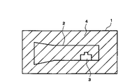
As shown in FIG. 1, a cantilever-shaped
[0031]
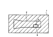
In parallel with this, a rectangular
[0032]
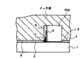
Thereafter, as shown in FIGS. 6 and 7, the
[0033]
Next, as shown in FIG. 8, the first substrate 1 on which the
[0034]
After the formation of the plating joint 11, the solvent-soluble resin layer formed as a plating base layer of the first insulating
[0035]
It should be noted that the vertical mirror structure according to the present invention is not limited to the one provided with the device substrate illustrated in FIG. 9, and a solvent-soluble resin layer formed as a plating underlayer of the
[0036]
The
[0037]
In the above-described embodiment, the plating
[0038]
Further, in the above-described embodiment, the nickel film serving as the base of the
[0039]
Furthermore, in the above-described embodiment, the patterning of the
[0040]
In addition, in the above-described embodiment, the pattern formation of the first insulating
[0041]
The vertical mirror of the present invention can be applied to various optical interconnection parts such as an optical switch and an optical connector. In addition, the manufacturing method of the present invention can be applied to manufacturing of various components in electronics and optoelectronics in addition to the vertical mirror. For example, an antenna having an efficient overhead wire structure can be easily manufactured by forming a high-frequency antenna pattern with a plating film and vertically standing on a substrate using this method. In addition, a structure in which a high-frequency transmission line is formed in the same manner as described above, stands upright on a substrate, and bends at 90 degrees as necessary, can be easily manufactured. A circuit can be manufactured.
[0042]
【The invention's effect】
As described above, the plating structure according to the present invention includes a first pattern and a second pattern formed of a metal film or an alloy film, and a plating product formed of a plating product that integrally joins the first and second patterns. Since it is formed from the joint portion, each portion of the plating structure can be formed thin. In addition, by arranging the second pattern perpendicular to the first pattern, a high vertical surface which cannot be formed by a conventional method such as the LIGA method can be arbitrarily formed. Can be a plated structure having a large height.
[0043]
Further, in the method of manufacturing a plated structure according to the present invention, after the first substrate having the first pattern and the second substrate having the second pattern are produced, the second substrate is temporarily fixed on the first substrate. Since the first pattern and the second pattern are joined at the plating joint, the first pattern and the second pattern can be joined by plating. For example, an expensive and large-scale device such as the case of using the LIGA method or the like. Since it is not necessary to use a complicated process, a plated structure having a required shape can be easily and efficiently manufactured. In addition, since the first insulating film, the second insulating film, and the second substrate are removed after the formation of the plating joint, a mirror surface having high flatness and flatness is formed on the surface from which the insulating film and the substrate are removed. Thus, a plated structure such as a vertical mirror having excellent optical characteristics can be manufactured.
[Brief description of the drawings]
FIG. 1 is a plan view of a first substrate on which a first pattern is formed.
FIG. 2 is a plan view of a first substrate on which a first insulating film is formed.
FIG. 3 is a plan view of a second substrate on which a second pattern is formed.
FIG. 4 is a plan view of a second substrate on which a second insulating film is formed.
FIG. 5 is a plan view of a second substrate showing cutout portions of individual pieces.
FIG. 6 is a plan view of a first substrate to which individual pieces are attached.
FIG. 7 is a side view of the first substrate to which the pieces are attached.
FIG. 8 is a side view of a first substrate to which individual pieces are attached, showing a method of forming a plating joint.
FIG. 9 is a side view of a vertical mirror structure having a device substrate.
FIG. 10 is a side view of a vertical mirror structure having no device substrate.
[Explanation of symbols]
REFERENCE SIGNS LIST 1
Claims (12)
前記第1パターンの一部に第1絶縁膜を被着し、前記第1パターンの他の一部に前記第1絶縁膜が被着されていない第1露出部を形成する工程と、
第2基板の片面に金属膜又は合金膜からなる第2パターンを形成する工程と、
前記第2パターンの一部に第2絶縁膜を被着し、前記第2パターンの他の一部に前記第2絶縁膜が被着されていない第2露出部を形成する工程と、
前記第1基板上に前記第2基板を仮固定し、前記第1露出部と前記第2露出部とを接近して配置する工程と、
前記第1露出部と前記第2露出部との間にメッキ接合部を生成する工程と、
前記第1絶縁膜、前記第2絶縁膜及び前記第2基板を除去する工程とを含むことを特徴とするメッキ構造体の製造方法。Forming a first pattern made of a metal film or an alloy film on one surface of the first substrate;
Forming a first exposed portion where the first insulating film is not applied to a part of the first pattern, and where the first insulating film is not applied to another part of the first pattern;
Forming a second pattern made of a metal film or an alloy film on one surface of the second substrate;
Forming a second exposed portion where the second insulating film is not applied to another part of the second pattern, wherein a second insulating film is applied to a part of the second pattern;
Temporarily fixing the second substrate on the first substrate, and disposing the first exposed portion and the second exposed portion close to each other;
Generating a plating joint between the first exposed portion and the second exposed portion;
Removing the first insulating film, the second insulating film, and the second substrate.
前記第1パターンの一部に第1絶縁膜を被着し、前記第1パターンの他の一部に前記第1絶縁膜が被着されていない第1露出部を形成する工程と、
第2基板の片面に金属膜又は合金膜からなる第2パターンを形成する工程と、
前記第2パターンの一部に第2絶縁膜を被着し、前記第2パターンの他の一部に前記第2絶縁膜が被着されていない第2露出部を形成する工程と、
前記第1基板上に前記第2基板を仮固定し、前記第1露出部と前記第2露出部とを接近して配置する工程と、
前記第1露出部と前記第2露出部との間にメッキ接合部を生成する工程と、
前記第1絶縁膜、前記第2絶縁膜、前記第1基板及び前記第2基板を除去する工程とを含むことを特徴とするメッキ構造体の製造方法。Forming a first pattern made of a metal film or an alloy film on one surface of the first substrate;
Forming a first exposed portion where the first insulating film is not applied to a part of the first pattern, and where the first insulating film is not applied to another part of the first pattern;
Forming a second pattern made of a metal film or an alloy film on one surface of the second substrate;
Forming a second exposed portion where the second insulating film is not applied to another part of the second pattern, wherein a second insulating film is applied to a part of the second pattern;
Temporarily fixing the second substrate on the first substrate, and disposing the first exposed portion and the second exposed portion close to each other;
Generating a plating joint between the first exposed portion and the second exposed portion;
Removing the first insulating film, the second insulating film, the first substrate, and the second substrate.
Priority Applications (1)
| Application Number | Priority Date | Filing Date | Title |
|---|---|---|---|
| JP2002168740A JP2004011000A (en) | 2002-06-10 | 2002-06-10 | Plated structure and its manufacturing method |
Applications Claiming Priority (1)
| Application Number | Priority Date | Filing Date | Title |
|---|---|---|---|
| JP2002168740A JP2004011000A (en) | 2002-06-10 | 2002-06-10 | Plated structure and its manufacturing method |
Publications (1)
| Publication Number | Publication Date |
|---|---|
| JP2004011000A true JP2004011000A (en) | 2004-01-15 |
Family
ID=30435569
Family Applications (1)
| Application Number | Title | Priority Date | Filing Date |
|---|---|---|---|
| JP2002168740A Withdrawn JP2004011000A (en) | 2002-06-10 | 2002-06-10 | Plated structure and its manufacturing method |
Country Status (1)
| Country | Link |
|---|---|
| JP (1) | JP2004011000A (en) |
Cited By (2)
| Publication number | Priority date | Publication date | Assignee | Title |
|---|---|---|---|---|
| EP1898611A1 (en) | 2004-01-19 | 2008-03-12 | Sharp Kabushiki Kaisha | Display of images and menu icons in a portable communication terminal |
| JP2010525647A (en) * | 2007-04-20 | 2010-07-22 | アイティーアイ スコットランド リミテッド | Ultra-wideband antenna |
-
2002
- 2002-06-10 JP JP2002168740A patent/JP2004011000A/en not_active Withdrawn
Cited By (2)
| Publication number | Priority date | Publication date | Assignee | Title |
|---|---|---|---|---|
| EP1898611A1 (en) | 2004-01-19 | 2008-03-12 | Sharp Kabushiki Kaisha | Display of images and menu icons in a portable communication terminal |
| JP2010525647A (en) * | 2007-04-20 | 2010-07-22 | アイティーアイ スコットランド リミテッド | Ultra-wideband antenna |
Similar Documents
| Publication | Publication Date | Title |
|---|---|---|
| KR100771030B1 (en) | Bump-attached wiring circuit board and method for manufacturing same | |
| US6562250B1 (en) | Method for manufacturing wiring circuit boards with bumps and method for forming bumps | |
| CN113777880A (en) | Micro LED device and preparation method thereof | |
| JP2003264359A (en) | Method for manufacturing microwave circuit base | |
| JPH06310833A (en) | Manufacture of electrical/optical wiring board | |
| JP2004011000A (en) | Plated structure and its manufacturing method | |
| US7666292B2 (en) | Method of manufacturing printed circuit board using imprinting process | |
| JP2012104521A (en) | Method of manufacturing circuit board | |
| KR100794544B1 (en) | Wiring circuit board having bumps and method of producing same | |
| JP4703065B2 (en) | Manufacturing method of optical waveguide circuit | |
| JPH10116861A (en) | Carrier tape and manufacture of carrier tape | |
| JP7226973B2 (en) | Substrate for forming via wiring, method for manufacturing substrate for forming via wiring, and method for mounting semiconductor chip | |
| JPH115289A (en) | Method and apparatus for producing print screen | |
| KR100275372B1 (en) | Method of manufacturing circuit board | |
| JP3061767B2 (en) | Tape carrier and manufacturing method thereof | |
| JP2727870B2 (en) | Film carrier tape and method of manufacturing the same | |
| JP2005005585A (en) | Flexible printed circuit board, flexible printed circuit board module, and method of producing flexible printed circuit board | |
| CN110035625B (en) | Method for manufacturing signal measurement medium soft board | |
| TW201010558A (en) | Preformed printed circuit board and mounting method for printed circuit board | |
| JP3651451B2 (en) | Probe unit and manufacturing method thereof | |
| JPH11297767A (en) | Film carrier tape | |
| JP4074287B2 (en) | Manufacturing method of probe unit | |
| JP2005183512A (en) | Method of transferring conductive portion and method of manufacturing wiring board | |
| CN113809266A (en) | Display substrate, manufacturing method thereof and display device | |
| JPH0218985A (en) | Manufacture of molding printed circuit board |
Legal Events
| Date | Code | Title | Description |
|---|---|---|---|
| A300 | Withdrawal of application because of no request for examination |
Free format text: JAPANESE INTERMEDIATE CODE: A300 Effective date: 20050906 |