EP4583659A2 - Devices having a transistor and a capacitor along a common horizontal level, and methods of forming devices - Google Patents
Devices having a transistor and a capacitor along a common horizontal level, and methods of forming devices Download PDFInfo
- Publication number
- EP4583659A2 EP4583659A2 EP25176032.8A EP25176032A EP4583659A2 EP 4583659 A2 EP4583659 A2 EP 4583659A2 EP 25176032 A EP25176032 A EP 25176032A EP 4583659 A2 EP4583659 A2 EP 4583659A2
- Authority
- EP
- European Patent Office
- Prior art keywords
- levels
- transistor
- assembly
- insulative
- along
- Prior art date
- Legal status (The legal status is an assumption and is not a legal conclusion. Google has not performed a legal analysis and makes no representation as to the accuracy of the status listed.)
- Pending
Links
Images

















Classifications
-
- H—ELECTRICITY
- H10—SEMICONDUCTOR DEVICES; ELECTRIC SOLID-STATE DEVICES NOT OTHERWISE PROVIDED FOR
- H10B—ELECTRONIC MEMORY DEVICES
- H10B12/00—Dynamic random access memory [DRAM] devices
- H10B12/30—DRAM devices comprising one-transistor - one-capacitor [1T-1C] memory cells
-
- H—ELECTRICITY
- H10—SEMICONDUCTOR DEVICES; ELECTRIC SOLID-STATE DEVICES NOT OTHERWISE PROVIDED FOR
- H10B—ELECTRONIC MEMORY DEVICES
- H10B12/00—Dynamic random access memory [DRAM] devices
- H10B12/01—Manufacture or treatment
- H10B12/02—Manufacture or treatment for one transistor one-capacitor [1T-1C] memory cells
-
- H—ELECTRICITY
- H10—SEMICONDUCTOR DEVICES; ELECTRIC SOLID-STATE DEVICES NOT OTHERWISE PROVIDED FOR
- H10B—ELECTRONIC MEMORY DEVICES
- H10B12/00—Dynamic random access memory [DRAM] devices
- H10B12/01—Manufacture or treatment
- H10B12/02—Manufacture or treatment for one transistor one-capacitor [1T-1C] memory cells
- H10B12/03—Making the capacitor or connections thereto
-
- H—ELECTRICITY
- H10—SEMICONDUCTOR DEVICES; ELECTRIC SOLID-STATE DEVICES NOT OTHERWISE PROVIDED FOR
- H10B—ELECTRONIC MEMORY DEVICES
- H10B12/00—Dynamic random access memory [DRAM] devices
- H10B12/01—Manufacture or treatment
- H10B12/02—Manufacture or treatment for one transistor one-capacitor [1T-1C] memory cells
- H10B12/05—Making the transistor
-
- H—ELECTRICITY
- H10—SEMICONDUCTOR DEVICES; ELECTRIC SOLID-STATE DEVICES NOT OTHERWISE PROVIDED FOR
- H10B—ELECTRONIC MEMORY DEVICES
- H10B12/00—Dynamic random access memory [DRAM] devices
- H10B12/30—DRAM devices comprising one-transistor - one-capacitor [1T-1C] memory cells
- H10B12/48—Data lines or contacts therefor
- H10B12/482—Bit lines
-
- H—ELECTRICITY
- H10—SEMICONDUCTOR DEVICES; ELECTRIC SOLID-STATE DEVICES NOT OTHERWISE PROVIDED FOR
- H10B—ELECTRONIC MEMORY DEVICES
- H10B12/00—Dynamic random access memory [DRAM] devices
- H10B12/30—DRAM devices comprising one-transistor - one-capacitor [1T-1C] memory cells
- H10B12/48—Data lines or contacts therefor
- H10B12/485—Bit line contacts
-
- H—ELECTRICITY
- H10—SEMICONDUCTOR DEVICES; ELECTRIC SOLID-STATE DEVICES NOT OTHERWISE PROVIDED FOR
- H10B—ELECTRONIC MEMORY DEVICES
- H10B12/00—Dynamic random access memory [DRAM] devices
- H10B12/30—DRAM devices comprising one-transistor - one-capacitor [1T-1C] memory cells
- H10B12/48—Data lines or contacts therefor
- H10B12/488—Word lines
-
- G—PHYSICS
- G11—INFORMATION STORAGE
- G11C—STATIC STORES
- G11C2211/00—Indexing scheme relating to digital stores characterized by the use of particular electric or magnetic storage elements; Storage elements therefor
- G11C2211/56—Indexing scheme relating to G11C11/56 and sub-groups for features not covered by these groups
- G11C2211/561—Multilevel memory cell aspects
-
- H—ELECTRICITY
- H10—SEMICONDUCTOR DEVICES; ELECTRIC SOLID-STATE DEVICES NOT OTHERWISE PROVIDED FOR
- H10B—ELECTRONIC MEMORY DEVICES
- H10B12/00—Dynamic random access memory [DRAM] devices
-
- H—ELECTRICITY
- H10—SEMICONDUCTOR DEVICES; ELECTRIC SOLID-STATE DEVICES NOT OTHERWISE PROVIDED FOR
- H10W—GENERIC PACKAGES, INTERCONNECTIONS, CONNECTORS OR OTHER CONSTRUCTIONAL DETAILS OF DEVICES COVERED BY CLASS H10
- H10W90/00—Package configurations
Definitions
- the DRAM unit cells may each comprise a capacitor in combination with a transistor. Charge stored on the capacitors of the DRAM unit cells may correspond to memory bits.
- Some embodiments include integrated devices having capacitors and transistors, with the capacitors being horizontally offset from the transistors.
- the integrated devices may be vertically stacked one atop another in an integrated assembly.
- the integrated devices may be memory cells of a DRAM array.
- Some embodiments include methods of forming integrated devices which have capacitors horizontally offset from transistors, and some embodiments include methods of forming architectures which comprise vertically-stacked tiers of such integrated devices. Example embodiments are described with reference to FIGS. 1-23 .
- a device 10 is illustrated to comprise a transistor 12 and a capacitor 14.
- the transistor 12 includes a gate 16, and a semiconductor material 18 adjacent the gate.
- the semiconductor material 18 includes a channel region 17.
- the channel region 17 is not visible in FIG. 1 , as it is under a portion of the gate 16; but an approximate location of the channel region is diagrammatically illustrated with a dashed arrow.
- the semiconductor material 18 also includes a first source/drain region 19 on one side of the channel region 17, and a second source/drain region 21 on an opposing side of the channel region from the first source/drain region 19.
- the transistor gate 16 comprises conductive material 20.
- conductive material may comprise any suitable electrically conductive composition(s), such as, for example, one or more of various metals (e.g., titanium, tungsten, cobalt, nickel, platinum, ruthenium, etc.), metal-containing compositions (e.g., metal silicide, metal nitride, metal carbide, etc.), and/or conductively-doped semiconductor materials (e.g., conductively-doped silicon, conductively-doped germanium, etc.).
- various metals e.g., titanium, tungsten, cobalt, nickel, platinum, ruthenium, etc.
- metal-containing compositions e.g., metal silicide, metal nitride, metal carbide, etc.
- conductively-doped semiconductor materials e.g., conductively-doped silicon, conductively-doped germanium, etc.
- the semiconductor material 18 may comprise any suitable composition or combination of compositions; such as, for example, one or more of silicon, germanium, III/V materials (e.g., gallium phosphide), semiconductor oxides, etc.
- the source/drain regions 19 and 21 may comprise conductively-doped regions.
- the channel region 17 may be doped to an appropriate level to achieve a desired threshold voltage.
- the capacitor 14 comprises a first electrode 22 and a second electrode 24.
- the electrodes 22 and 24 are spaced from one another, and dielectric material would be between the first and second electrodes.
- the dielectric material is not shown in FIG. 1 in order to simplify the drawing, but would be similar to the dielectric material 128 described below with reference to FIG. 23 .
- the electrodes 22 and 24 comprise conductive materials 28 and 30, respectively.
- Such conductive materials may comprise any suitable electrically conductive composition(s), such as, for example, one or more of various metals (e.g., titanium, tungsten, cobalt, nickel, platinum, ruthenium, etc.), metal-containing compositions (e.g., metal silicide, metal nitride, metal carbide, etc.), and/or conductively-doped semiconductor materials (e.g., conductively-doped silicon, conductively-doped germanium, etc.).
- the conductive materials 28 and 30 may be the same as one another in some embodiments, and may be different from one another in other embodiments.
- the electrodes 22 and 24 may be respectively referred to as a bottom electrode and a top electrode, a storage node electrode and a plate electrode, a bottom plate and a top plate, etc.
- the second source/drain region 21 is coupled with the first electrode 22 of the capacitor 14; and in the illustrated embodiment is directly against the first electrode 22.
- a bitline 32 extends through the device 10, and is coupled with the first source/drain region 19. In the illustrated embodiment, the first source/drain region 19 is directly against the bitline 32.
- the bitline 32 comprises conductive material 34.
- the conductive material 34 may comprise any suitable electrically conductive composition(s), such as, for example, one or more of various metals (e.g., titanium, tungsten, cobalt, nickel, platinum, ruthenium, etc.), metal-containing compositions (e.g., metal silicide, metal nitride, metal carbide, etc.), and/or conductively-doped semiconductor materials (e.g., conductively-doped silicon, conductively-doped germanium, etc.).
- various metals e.g., titanium, tungsten, cobalt, nickel, platinum, ruthenium, etc.
- metal-containing compositions e.g., metal silicide, metal nitride, metal carbide, etc.
- conductively-doped semiconductor materials e.g., conductively-doped silicon, conductively-doped germanium, etc.
- a wordline 36 is coupled with the gate 12.
- the device 10 may correspond to a memory cell, and may be one of many memory cells of a memory array (for instance, a DRAM array).
- the memory cell 10 may be addressed (i.e., read from/written to) utilizing the wordline 36 and the bitline 32.
- the device 10 may comprise numerous insulative materials which are not shown in the diagram of FIG. 1 in order to simplify the drawing.
- the capacitor dielectric material i.e., the material 128 shown in FIG. 23
- gate dielectric material would be provided between the gate and the channel region 17 (example gate dielectric material is shown in FIG. 19 as material 38).
- insulative materials would be provided to surround the device 10, and to isolate the bitline 32 from the capacitor 14.
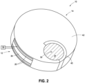
- FIG. 2 shows insulative material 40 provided between the bitline 32 and the capacitor 14, and shows insulative material 42 over the transistor 12 and the capacitor 14.
- the insulative materials 40 and 42 may comprise any suitable composition(s); and in some embodiments may comprise one or more of silicon dioxide, silicon nitride, high-k oxides (with high-k meaning a dielectric constant greater than that of silicon dioxide), etc.
- the insulative materials 40 and 42 may be the same composition as one another in some embodiments, and may be different compositions relative to one another in other embodiments. Further, in some embodiments either or both of the materials 40 and 42 may comprise two or more different materials, rather than the single homogeneous materials illustrated in FIG. 2 .
- the bitline 32 may have a different configuration than shown in FIG. 1 .
- FIG. 1 shows the bitline 32 configured to be substantially circular along a horizontal cross-section through the bitline.
- the bitline may be polygonal, square, rectangular, elliptical, etc.
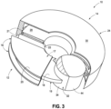
- FIG. 3 shows a configuration in which the bitline 32 is crescent-shaped along a horizontal cross-section through the bitline.
- the crescent-shaped bitline is along an insulative material 44.
- Such insulative material may comprise, for example, any of the compositions discussed above with reference to FIG. 2 for the insulative materials 40 and 42.
- the insulative material 44 may be the same as one or both of the insulative materials 40 and 42.
- the devices 10 of FIGS. 1-5 have the capacitor 14 horizontally-offset relative to the transistor 12. Also, all of the devices are substantially circular along horizontal cross-sections through the devices (with the term "substantially circular” meaning circular to within reasonable tolerances of fabrication and measurement). The devices may have other shapes in other embodiments, as discussed in more detail below with reference to FIG. 8 .
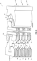
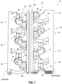
- FIG. 6 shows an example memory array 50 comprising memory cells 10a-f having the configuration of the device 10 of FIG. 1 .
- Each memory cell comprises a capacitor (e.g., the capacitors 14a-c visible in FIG. 6 ) coupled with an associated transistor (e.g., the transistors 12a-12c visible in FIG. 6 ).
- the capacitors are vertically-stacked one atop another along levels 52, 54 and 56.
- the level 52 comprises the memory cells 10a and 10d;
- the level 54 comprises the memory cells 10b and 10e;
- the level 56 comprises the memory cells 10c and 10f.
- Insulative materials are not shown in FIG. 6 in order to simplify the drawing, but it is to be understood that insulative materials analogous those described above with reference to FIGS. 1 and 2 (e.g., capacitor dielectric material, gate dielectric material, etc.) would be provided.
- Wordlines (e.g., access lines, etc.) 36a-f extend horizontally, and are coupled with transistor gates of the memory cells 10a-f (the transistor gates are not labeled in FIG. 6 , but would be analogous to the transistor gate 16 of FIG. 1 ).
- Each memory cell 10a-f may be uniquely addressed through a combination of one of the digit lines (32a, 32b), and one of the wordlines (36a-f).
- the wordlines may be considered to extend along rows of the array of memory cells
- the digit lines may be considered to extend along columns of the array of memory cells.
- the memory cells within each level may be substantially identical to one another (with the term "substantially identical” meaning identical to within reasonable tolerances of fabrication and measurement). Further, at least some of the memory cells within one vertical level (e.g., level 52) may be substantially identical to memory cells within another vertical level (e.g., level 54). In some embodiments, all of the memory cells within one vertical level may be substantially identical to all of the memory cells within another vertical level. In some embodiments, all of the memory cells within all of the vertical levels may be substantially identical to one another.
- At least some of the memory cells within one vertical level may not be substantially identical to at least some of the memory cells within another vertical level. Such may enable different vertical levels to be tailored for different applications. Differences between the memory cells in one vertical level relative to the memory cells in another vertical level may provide different performance characteristics amongst transistors of the memory cells (such as, for example, differences in one or more of effective gate width, effective gate length, threshold voltage, on-current, off-current, etc.) and/or different performance characteristics amongst capacitors of the memory cells (such as, for example, differences in capacitance).
- differences in performance characteristics amongst transistors of the memory cells may be achieved by providing different semiconductor material within one level as compared to another level (e.g., the semiconductor material 18a may be different relative to the semiconductor material 18b); with the differences between the semiconductor materials being differences in composition, differences in thickness, and/or differences in any other suitable physical characteristics.
- differences in performance characteristics between one level and another may be achieved by providing different dopants and/or dopant concentrations within the semiconductor material of one level as compared to the semiconductor material of another level (e.g., by providing different dopant and/or dopant concentrations within the semiconductor material 18a as compared to the semiconductor material 18b).
- Differences in performance characteristics amongst capacitors of different levels may be achieved by, for example, forming the electrodes to be of different shapes amongst the capacitors, utilizing different materials for capacitor dielectric amongst the capacitors and/or by utilizing different thicknesses of capacitor dielectric amongst the capacitors.
- FIG. 7 shows another view of a region of the memory array 50, and shows a pair of adjacent rows 58 and 60 along the level 52. Insulative materials are not shown in FIG. 7 in order to simplify the drawing, but it is to be understood that insulative materials analogous those described above with reference to FIGS. 1 and 2 (e.g., capacitor dielectric material, gate dielectric material, etc.) would be provided.
- the row 58 comprises memory cells 10a, 10g and 10h; and the row 60 comprises memory cells 10d, 10i, 10j and 10k.
- the embodiment of FIG. 7 illustrates one example arrangement of digit lines (32a-f), and wordlines (36a and 36d) relative to the memory cells. Other arrangements may be utilized in other embodiments.
- FIGS. 1-7 are illustrated to be substantially circular along horizontal cross-sections through the memory cells, it is to be understood that in other embodiments the memory cells may have other configurations.
- FIG. 8 shows a top view of a memory cell 10 in a configuration in which the memory cell has a polygonal shape along a horizontal cross-section through the memory cell.
- the memory cell is substantially square along the horizontal cross-section through the memory cell.
- the memory cell may have any other suitable shape.
- the devices 10 of FIGS. 1-8 may be fabricated with any suitable processing.
- the devices are fabricated by providing holes through a stack of materials.
- the transistors are formed along a side of the holes, and the capacitors are formed along other sides of the holes.
- FIG. 9 shows a top view of a construction 62 illustrating example locations 64 for holes 86 (only some which are labeled) utilized during fabrication devices.
- the holes 86 are lined with a material 96, which is described in more detail below with reference to FIG. 13 .
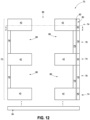
- FIG. 9 also shows locations 66 where slits will be formed for fabrication of the transistor gates and wordlines, and shows locations 68 where slits will be formed for fabrication of the capacitors.
- FIG. 9 is provided to provide the reader with an overview of an example method for fabricating an array of devices (e.g., the example devices 10 of FIGS. 1-8 ) in accordance with an example embodiment.
- the devices may be fabricated utilizing other constructions.
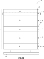
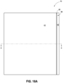
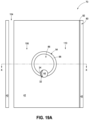
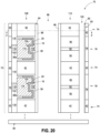
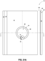
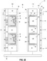
- FIGS. 10-23 and 10A-23A An example method for fabricating devices analogous to the device 10 of FIG. 3 is described with reference to FIGS. 10-23 and 10A-23A .
- the views of FIGS. 10A-23A are along the cross-sections Z-Z of FIGS. 10-23 , respectively; and the views of FIGS. 10-23 are along the lines X-X of FIGS. 10A-23A , respectively. It is to be understood that the example method of FIGS. 10-23 and 10A-23A may be modified to fabricate any of the devices of FIGS. 1-8 , or analogous devices.
- an assembly 70 comprises a stack 72 of first levels 74 and second levels 76.
- the levels 74 and 76 alternate with one another along a vertical direction.
- the second levels 76 may be referred to as device levels, since integrated devices are eventually formed within the second levels 76.
- the stack 72 is supported by a base 84.
- the base 84 may comprise semiconductor material; and may, for example, comprise, consist essentially of, or consist of monocrystalline silicon.
- the base 84 may be referred to as a semiconductor substrate.
- semiconductor substrate means any construction comprising semiconductive material, including, but not limited to, bulk semiconductive materials such as a semiconductive wafer (either alone or in assemblies comprising other materials), and semiconductive material layers (either alone or in assemblies comprising other materials).
- substrate refers to any supporting structure, including, but not limited to, the semiconductor substrates described above.
- the base 84 may correspond to a semiconductor substrate containing one or more materials associated with integrated circuit fabrication. Such materials may include, for example, one or more of refractory metal materials, barrier materials, diffusion materials, insulator materials, etc.
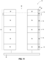
- an opening 86 is formed through the stack 72.
- the opening 86 may be referred to as a first opening, and may be representative of a plurality of openings formed through the stack 74 (a plurality of openings 86 is shown in FIG. 9 , and discussed above). Only a single opening 86 is shown in the views of FIGS. 11 and 11A in order to simplify the drawings, but it is to be understood that such opening may be one of a large number of substantially identical openings formed through the stack.
- sacrificial materials 90 and 92 are formed within the cavities 88, and then an insulative liner 94 is formed along a peripheral boundary of the opening 86.
- a layer of the first material 92 is provided between a pair of layers of the second material 90 within each of the cavities 88.
- the liner 94 comprises an insulative material 96.
- the material 96 may comprise any suitable composition or combination of compositions; and in some embodiments may comprise, consist essentially of, or consist of silicon nitride.
- construction 70 is shown at a processing stage subsequent to that of FIG. 13A .
- a second opening 98 is formed overlapping a region of the first opening 86, and the second opening 98 is filled with a digit line template 100.
- the digit line template 100 extends vertically through the stack 72.
- the digit line template comprises two materials 44 and 102.
- the material 44 may comprise any of the insulative compositions described above with reference to FIG. 3 .
- the material 102 is a sacrificial material, and in some embodiments may comprise, consist essentially of, or consist of phosphosilicate glass.
- the illustrated digit line template 100 comprising the two materials 44 and 102 will ultimately form a digit line 32 having the configuration shown in FIG.
- the digit line template 100 may comprise only the sacrificial material 102, and may be utilized to form a digit line 32 having the configuration shown in FIG. 1 as being circular shaped along a horizontal cross-section.
- the sacrificial material 102 may be in any other suitable shape for forming a desired digit line configuration.
- the sacrificial material 92 is removed from along the slit 104 to form horizontally-extending voids 108. Such removal may be accomplished by passing appropriate etchant into the slit 104, and utilizing a timed etch to remove a desired amount of the sacrificial material 92.
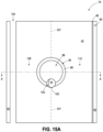
- the voids 108 may be formed to extend about halfway around opening 86. Such is diagrammatically illustrated in the top view of FIG. 15A utilizing a dashed line 107 to illustrate approximate lateral boundaries (i.e., edges) of the voids 108 within the stack 72.
- the sacrificial material 102 of the digit line template 100 may comprise a same composition as the sacrificial material 92 (e.g., both may comprise phosphosilicate glass). Accordingly, the sacrificial material 102 of the digit line template 100 may be removed simultaneously with the removal of the sacrificial material 92 to leave a void 103.
- semiconductor material 18 is provided within the horizontally-extending voids 108 ( FIG. 15 ), and such semiconductor material replaces the sacrificial material 92 which had been removed to form such voids.
- the semiconductor material 18 may abut the sacrificial material 92 along the edges of the previous voids 108 (with such edges being diagrammatically illustrated as being approximately along a location of the dashed line 107 of FIG. 16A).
- FIG. 16B shows a region along the edge within one of the levels 76 of stack 72, and shows the semiconductor material 18 directly against the sacrificial material 92.
- construction 70 may be heated or otherwise operably processed to cause out-diffusion of phosphorus from phosphosilicate glass of sacrificial material 92 into the semiconductor material 18 to form the first source/drain region 19; and to cause out-diffusion from conductively-doped semiconductor material of the digit line 32 into the semiconductor material 18 to form the second source/drain region 21.
- the semiconductor material 18 is shown to be the same in all of the vertically-stacked levels 76, in other embodiments the semiconductor material within one of the vertically-stacked levels 76 may be different than that within another of the vertically-stacked levels 76. Such may enable fabrication of vertically-stacked transistor devices having different performance characteristics relative to one another; with the vertically-stacked transistor devices being shown in FIG. 20 as devices 12a and 12b.
- the sacrificial material 90 is removed from along the first side 106 of the opening 86, together with a portion of the semiconductor material 18, to leave cavities 112. Such removal may be accomplished by flowing one or more suitable etchants into the slit 104.
- gate dielectric material 38 is deposited within the voids 112.
- the gate dielectric material 38 may comprise any suitable composition(s); and in some embodiments may comprise, consist essentially of, or consist of silicon dioxide.
- gate material 20 and wordline material 114 are formed within the voids 112 ( FIG. 18 ).
- the gate material 20 and wordline material 114 may comprise any suitable compositions, and may be the same as one another or different from one another.
- the gate material 20 may comprise, consist essentially of, or consist of tungsten; and the wordline material 114 may comprise a conductive material to which the tungsten may be selectively etched.
- the wordline material 114 may comprise, consist essentially of, or consist of titanium nitride.
- the gate material 20 forms transistor gates 16.
- the gate dielectric material 38, semiconductor material 18 and gate material 20 together form transistor devices 12a and 12b along the first side 106 of the opening 86.
- the semiconductor material 18 comprises the channel regions 17 extending along the gates 16, and also comprises the source/drain regions 19 and 21 (shown in FIGS. 1 and 3 , but not visible in FIGS. 19 and 19A ).
- insulative material 116 and conductive material 118 are formed within the slit 104 ( FIGS. 19 and 19A ).
- the insulative material 116 may comprise any suitable composition or combination of compositions; and in some embodiments may comprise, consist essentially of, or consist of one or more of silicon dioxide, silicon nitride, etc.
- the insulative material 116 may be a same composition as the insulative material 42 in some embodiments.
Landscapes
- Engineering & Computer Science (AREA)
- Manufacturing & Machinery (AREA)
- Semiconductor Memories (AREA)
- Physics & Mathematics (AREA)
- Geometry (AREA)
- Metal-Oxide And Bipolar Metal-Oxide Semiconductor Integrated Circuits (AREA)
Abstract
a first insulative level over a semiconductor base;
a second insulative level over the first insulative level; and
a device between the first and second insulative levels; the device including a transistor coupled with a capacitor; the capacitor being horizontally offset relative to the transistor; the capacitor and the transistor being in a same planar level as one another; wherein the transistor includes a gate proximate a channel region, and wherein the gate brackets the channel region.
Description
- Devices which have a transistor and a capacitor; and in which the transistor and the capacitor are along a common horizontal level. Methods of forming devices in which a transistor and an associated capacitor of a memory cell are both along the same horizontal level as one another.
- Memory is one type of integrated circuitry, and is used in electronic systems for storing data. Integrated memory is usually fabricated in one or more arrays of individual memory cells. The memory cells are configured to retain or store memory in at least two different selectable states. In a binary system, the states are considered as either a "0" or a "1". In other systems, at least some individual memory cells may be configured to store more than two levels or states of information.
- An example memory is dynamic random access memory (DRAM). The DRAM unit cells may each comprise a capacitor in combination with a transistor. Charge stored on the capacitors of the DRAM unit cells may correspond to memory bits.
- There is a continuing goal to improve architectural layouts of integrated circuit structures in an effort to maintain (or even improve) device performance, while achieving ever higher levels of integration. It is desired to develop improved architectures, and improved devices. It would be desirable for the improved devices to be suitable for utilization in memory and/or in other integrated circuitry. It is further desired to develop methods for fabricating the improved devices and architectures.
-
-
FIG. 1 is a diagrammatic three-dimensional view of an example device. -
FIG. 2 is another diagrammatic three-dimensional view of the example device ofFIG. 1 . -
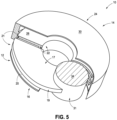
FIGS. 3-5 are diagrammatic three-dimensional views of other example devices. -
FIG. 6 is a diagrammatic three-dimensional view of a region of an example memory array. -
FIG. 7 is another diagrammatic three-dimensional view of a region of the example memory array ofFIG. 6 . -
FIG. 8 is a diagrammatic top view of another example device. -
FIG. 9 is a diagrammatic top view of an example assembly at an example process stage. -
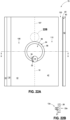
FIGS. 10-23 are diagrammatic cross-sectional side views of a region of an example assembly at example process stages. -
FIGS. 10A-23A are diagrammatic top-down sectional views of the regions of the example assembly at the example process stages ofFIGS. 10-23 . The views ofFIGS. 10-23 are along the lines X-X ofFIGS. 10A-23A , and the views ofFIGS. 10A-23A are along the lines Z-Z ofFIGS. 10-23 . -
FIG. 13B is a diagrammatic top-down sectional view of the example assembly ofFIG. 13A at an example process stage subsequent to that ofFIG. 13A . -
FIGS. 16B and 16C are diagrammatic cross-sectional views of example structures that may be within regions labeled 16A and 16B in the top-down viewFIG. 16A . -
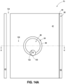
FIG. 22B is a diagrammatic cross-sectional view of an example structure that may be within a region labeled 22B in the top-down viewFIG. 22A . - Some embodiments include integrated devices having capacitors and transistors, with the capacitors being horizontally offset from the transistors. The integrated devices may be vertically stacked one atop another in an integrated assembly. In some embodiments, the integrated devices may be memory cells of a DRAM array. Some embodiments include methods of forming integrated devices which have capacitors horizontally offset from transistors, and some embodiments include methods of forming architectures which comprise vertically-stacked tiers of such integrated devices. Example embodiments are described with reference to
FIGS. 1-23 . - Referring to
FIG. 1 , adevice 10 is illustrated to comprise atransistor 12 and acapacitor 14. - The
transistor 12 includes agate 16, and asemiconductor material 18 adjacent the gate. Thesemiconductor material 18 includes achannel region 17. Thechannel region 17 is not visible inFIG. 1 , as it is under a portion of thegate 16; but an approximate location of the channel region is diagrammatically illustrated with a dashed arrow. Thesemiconductor material 18 also includes a first source/drain region 19 on one side of thechannel region 17, and a second source/drain region 21 on an opposing side of the channel region from the first source/drain region 19. - The
transistor gate 16 comprisesconductive material 20. Such conductive material may comprise any suitable electrically conductive composition(s), such as, for example, one or more of various metals (e.g., titanium, tungsten, cobalt, nickel, platinum, ruthenium, etc.), metal-containing compositions (e.g., metal silicide, metal nitride, metal carbide, etc.), and/or conductively-doped semiconductor materials (e.g., conductively-doped silicon, conductively-doped germanium, etc.). - The
semiconductor material 18 may comprise any suitable composition or combination of compositions; such as, for example, one or more of silicon, germanium, III/V materials (e.g., gallium phosphide), semiconductor oxides, etc. The source/drain regions channel region 17 may be doped to an appropriate level to achieve a desired threshold voltage. - The
capacitor 14 comprises afirst electrode 22 and asecond electrode 24. Theelectrodes FIG. 1 in order to simplify the drawing, but would be similar to thedielectric material 128 described below with reference toFIG. 23 . - The
electrodes conductive materials conductive materials - In some embodiments, the
electrodes - The second source/
drain region 21 is coupled with thefirst electrode 22 of thecapacitor 14; and in the illustrated embodiment is directly against thefirst electrode 22. - A
bitline 32 extends through thedevice 10, and is coupled with the first source/drain region 19. In the illustrated embodiment, the first source/drain region 19 is directly against thebitline 32. - The
bitline 32 comprisesconductive material 34. Theconductive material 34 may comprise any suitable electrically conductive composition(s), such as, for example, one or more of various metals (e.g., titanium, tungsten, cobalt, nickel, platinum, ruthenium, etc.), metal-containing compositions (e.g., metal silicide, metal nitride, metal carbide, etc.), and/or conductively-doped semiconductor materials (e.g., conductively-doped silicon, conductively-doped germanium, etc.). - A
wordline 36 is coupled with thegate 12. In some embodiments, thedevice 10 may correspond to a memory cell, and may be one of many memory cells of a memory array (for instance, a DRAM array). Thememory cell 10 may be addressed (i.e., read from/written to) utilizing thewordline 36 and thebitline 32. - The
device 10 may comprise numerous insulative materials which are not shown in the diagram ofFIG. 1 in order to simplify the drawing. For instance, the capacitor dielectric material (i.e., thematerial 128 shown inFIG. 23 ) has already been mentioned. Also, gate dielectric material would be provided between the gate and the channel region 17 (example gate dielectric material is shown inFIG. 19 as material 38). Further, insulative materials would be provided to surround thedevice 10, and to isolate thebitline 32 from thecapacitor 14. For instance,FIG. 2 shows insulative material 40 provided between thebitline 32 and thecapacitor 14, and showsinsulative material 42 over thetransistor 12 and thecapacitor 14. - The
insulative materials insulative materials materials FIG. 2 . - In some embodiments, the
bitline 32 may have a different configuration than shown inFIG. 1 . Specifically,FIG. 1 shows thebitline 32 configured to be substantially circular along a horizontal cross-section through the bitline. In other embodiments, the bitline may be polygonal, square, rectangular, elliptical, etc.FIG. 3 shows a configuration in which thebitline 32 is crescent-shaped along a horizontal cross-section through the bitline. The crescent-shaped bitline is along aninsulative material 44. Such insulative material may comprise, for example, any of the compositions discussed above with reference toFIG. 2 for theinsulative materials insulative material 44 may be the same as one or both of theinsulative materials - The
gate 16 ofFIGS. 1 and3 is illustrated to be in a configuration which brackets thechannel region 17 withinsemiconductor material 18. In other embodiments, thegate 16 may have a different configuration. For instance,FIG. 4 shows a configuration in which thegate 16 is primarily over thechannel region 17, andFIG. 5 shows a configuration in which thegate 16 is primarily under thechannel region 17. Accordingly,FIGS. 4 and5 show configurations in which thegate 16 is along one side of thechannel region 17, rather than being along two opposing sides of the channel region (i.e., rather than bracketing the channel region). - The
devices 10 ofFIGS. 1-5 have thecapacitor 14 horizontally-offset relative to thetransistor 12. Also, all of the devices are substantially circular along horizontal cross-sections through the devices (with the term "substantially circular" meaning circular to within reasonable tolerances of fabrication and measurement). The devices may have other shapes in other embodiments, as discussed in more detail below with reference toFIG. 8 . - The
devices 10 ofFIGS. 1-5 may be utilized as memory cells within memory arrays. For instance,FIG. 6 , shows anexample memory array 50 comprisingmemory cells 10a-f having the configuration of thedevice 10 ofFIG. 1 . Each memory cell comprises a capacitor (e.g., thecapacitors 14a-c visible inFIG. 6 ) coupled with an associated transistor (e.g., thetransistors 12a-12c visible inFIG. 6 ). The capacitors are vertically-stacked one atop another alonglevels level 52 comprises thememory cells level 54 comprises thememory cells level 56 comprises thememory cells FIG. 6 in order to simplify the drawing, but it is to be understood that insulative materials analogous those described above with reference toFIGS. 1 and2 (e.g., capacitor dielectric material, gate dielectric material, etc.) would be provided. - The capacitors comprise the first electrodes (for instance, the
electrodes electrodes electrodes electrodes 24d, 24e and 24f are within a common plate labeled 24d/24e/24f. Thecommon plates 24a/24b/24c and 24d/24e/24f may be coupled with one another in some embodiments, and may be held at any suitable voltage (i.e., ground, Vcc/2, etc.). - Wordlines (e.g., access lines, etc.) 36a-f extend horizontally, and are coupled with transistor gates of the
memory cells 10a-f (the transistor gates are not labeled inFIG. 6 , but would be analogous to thetransistor gate 16 ofFIG. 1 ). - Digit lines (e.g. bitlines, senses lines, etc.) extend vertically and are coupled with source/drain regions of the
memory cells 10a-f (the source/drain regions are not labeled inFIG. 6 , but the digit lines would be coupled to source/drain regions analogous to the source/drain region 19 ofFIG. 1 ). - Each
memory cell 10a-f may be uniquely addressed through a combination of one of the digit lines (32a, 32b), and one of the wordlines (36a-f). In some embodiments, the wordlines may be considered to extend along rows of the array of memory cells, and the digit lines may be considered to extend along columns of the array of memory cells. -
FIG. 6 shows a region of thememory array 50, and the memory array may comprise numerous other memory cells besides the illustrated sixmemory cells 10a-f. The memory array may extend vertically above and below the illustrated region, and may extend laterally to the left and right of the illustrated region, as well as into and out of the page relative to the illustrated region. The memory array may comprise any suitable number of memory cells; and in some embodiments may comprise hundreds, thousands, millions, billions, etc., of memory cells. - The memory cells within each level (e.g., the
levels - In some embodiments, at least some of the memory cells within one vertical level may not be substantially identical to at least some of the memory cells within another vertical level. Such may enable different vertical levels to be tailored for different applications. Differences between the memory cells in one vertical level relative to the memory cells in another vertical level may provide different performance characteristics amongst transistors of the memory cells (such as, for example, differences in one or more of effective gate width, effective gate length, threshold voltage, on-current, off-current, etc.) and/or different performance characteristics amongst capacitors of the memory cells (such as, for example, differences in capacitance).
- In some embodiments, differences in performance characteristics amongst transistors of the memory cells may be achieved by providing different semiconductor material within one level as compared to another level (e.g., the
semiconductor material 18a may be different relative to thesemiconductor material 18b); with the differences between the semiconductor materials being differences in composition, differences in thickness, and/or differences in any other suitable physical characteristics. Alternatively, or additionally, differences in performance characteristics between one level and another may be achieved by providing different dopants and/or dopant concentrations within the semiconductor material of one level as compared to the semiconductor material of another level (e.g., by providing different dopant and/or dopant concentrations within thesemiconductor material 18a as compared to thesemiconductor material 18b). Differences in performance characteristics amongst capacitors of different levels may be achieved by, for example, forming the electrodes to be of different shapes amongst the capacitors, utilizing different materials for capacitor dielectric amongst the capacitors and/or by utilizing different thicknesses of capacitor dielectric amongst the capacitors. -
FIG. 7 shows another view of a region of thememory array 50, and shows a pair ofadjacent rows level 52. Insulative materials are not shown inFIG. 7 in order to simplify the drawing, but it is to be understood that insulative materials analogous those described above with reference toFIGS. 1 and2 (e.g., capacitor dielectric material, gate dielectric material, etc.) would be provided. - The
row 58 comprisesmemory cells row 60 comprisesmemory cells FIG. 7 illustrates one example arrangement of digit lines (32a-f), and wordlines (36a and 36d) relative to the memory cells. Other arrangements may be utilized in other embodiments. - Although the memory cells (i.e., devices) of
FIGS. 1-7 are illustrated to be substantially circular along horizontal cross-sections through the memory cells, it is to be understood that in other embodiments the memory cells may have other configurations. For instance,FIG. 8 shows a top view of amemory cell 10 in a configuration in which the memory cell has a polygonal shape along a horizontal cross-section through the memory cell. In the illustrated embodiment, the memory cell is substantially square along the horizontal cross-section through the memory cell. In other embodiments, the memory cell may have any other suitable shape. - Insulative materials are not shown in
FIG. 8 in order to simplify the drawing, but it is to be understood that insulative materials analogous those described above with reference toFIGS. 1 and2 (e.g., capacitor dielectric material, gate dielectric material, etc.) would be provided. - The
devices 10 ofFIGS. 1-8 may be fabricated with any suitable processing. In some embodiments, the devices are fabricated by providing holes through a stack of materials. The transistors are formed along a side of the holes, and the capacitors are formed along other sides of the holes.FIG. 9 shows a top view of aconstruction 62 illustratingexample locations 64 for holes 86 (only some which are labeled) utilized during fabrication devices. Theholes 86 are lined with amaterial 96, which is described in more detail below with reference toFIG. 13 .FIG. 9 also showslocations 66 where slits will be formed for fabrication of the transistor gates and wordlines, and showslocations 68 where slits will be formed for fabrication of the capacitors. Theconstruction 62 ofFIG. 9 is provided to provide the reader with an overview of an example method for fabricating an array of devices (e.g., theexample devices 10 ofFIGS. 1-8 ) in accordance with an example embodiment. In other embodiments, the devices may be fabricated utilizing other constructions. - An example method for fabricating devices analogous to the
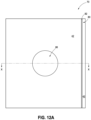
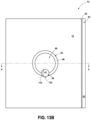
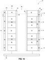
device 10 ofFIG. 3 is described with reference toFIGS. 10-23 and10A-23A . The views ofFIGS. 10A-23A are along the cross-sections Z-Z ofFIGS. 10-23 , respectively; and the views ofFIGS. 10-23 are along the lines X-X ofFIGS. 10A-23A , respectively. It is to be understood that the example method ofFIGS. 10-23 and10A-23A may be modified to fabricate any of the devices ofFIGS. 1-8 , or analogous devices. - Referring to
FIGS. 10 and10A , anassembly 70 comprises astack 72 offirst levels 74 andsecond levels 76. Thelevels - The
first levels 74 may compriseinsulative material 42, and may be referred to as insulative levels. Theinsulative material 42 may comprise any suitable composition(s); and in some embodiments may comprise, consist essentially of, or consist of silicon nitride. Theinsulative material 42 offirst levels 74 may be the same as that described above with reference toFIG. 2 . - The
second levels 76 comprisesacrificial material 78. Thesacrificial material 78 is a material selectively removable relative to theinsulative material 42. In some embodiments, thesacrificial material 78 may comprise, consist essentially of, or consist of silicon dioxide. For instance, thesacrificial material 78 may comprise silicon dioxide which is effectively not doped with boron, phosphorus, or other dopants. Such sacrificial material may be referred to as a non-doped silicate glass (NSG). It may be difficult to have absolutely no dopant within silicate glass, and thus the NSG is referred to as being "effectively not doped". In some embodiments, the dopant level of the NSG may be less than or equal to about 1015 atoms/cm3. - The
second levels 76 may be referred to as device levels, since integrated devices are eventually formed within thesecond levels 76. - An
insulative panel 80 extends through thestack 72. Theinsulative panel 80 comprises aninsulative material 82. Thematerial 82 may comprise any suitable composition or combination of compositions; and in some embodiments may comprise a same composition as theinsulative material 42. For instance, thematerials panel 80 may be utilized to define edges of capacitors at processing stages described below with reference toFIGS. 20 and21 . In some embodiments, such edges may be defined without utilization of thepanel 80; and accordingly thepanel 80 may be omitted. - The
stack 72 is supported by abase 84. The base 84 may comprise semiconductor material; and may, for example, comprise, consist essentially of, or consist of monocrystalline silicon. The base 84 may be referred to as a semiconductor substrate. The term "semiconductor substrate" means any construction comprising semiconductive material, including, but not limited to, bulk semiconductive materials such as a semiconductive wafer (either alone or in assemblies comprising other materials), and semiconductive material layers (either alone or in assemblies comprising other materials). The term "substrate" refers to any supporting structure, including, but not limited to, the semiconductor substrates described above. In some applications, thebase 84 may correspond to a semiconductor substrate containing one or more materials associated with integrated circuit fabrication. Such materials may include, for example, one or more of refractory metal materials, barrier materials, diffusion materials, insulator materials, etc. - A gap is provided between the
stack 72 and the base 84 to indicate that there may be other materials, components, etc., provided between thestack 22 and the base 84 in some embodiments. Alternatively, thestack 72 may be provided directly against an upper surface of thebase 84. - Referring to
FIGS. 11 and11A , anopening 86 is formed through thestack 72. Theopening 86 may be referred to as a first opening, and may be representative of a plurality of openings formed through the stack 74 (a plurality ofopenings 86 is shown inFIG. 9 , and discussed above). Only asingle opening 86 is shown in the views ofFIGS. 11 and11A in order to simplify the drawings, but it is to be understood that such opening may be one of a large number of substantially identical openings formed through the stack. - Referring to
FIGS. 12 and12A , thesacrificial material 78 is recessed relative to theinsulative material 42 to formcavities 88. - Referring to
FIGS. 13 and13A ,sacrificial materials cavities 88, and then aninsulative liner 94 is formed along a peripheral boundary of theopening 86. In the illustrated embodiment, a layer of thefirst material 92 is provided between a pair of layers of thesecond material 90 within each of thecavities 88. - The
sacrificial materials sacrificial material 92 be selectively removable relative to the firstsacrificial material 90. In some embodiments, thesacrificial material 90 may comprise, consist essentially of, or consist of NSG, and may be the same as thesacrificial material 78. Thesacrificial material 92 may comprise a doped silicate glass; and in some embodiments may comprise, consist essentially of, or consist of phosphosilicate glass. The doped silicate glass comprises a higher concentration of dopant (e.g., phosphorus) than the NSG, and in some embodiments may comprise a dopant concentration of at least about 1016 atoms/cm3. - The
liner 94 comprises aninsulative material 96. Thematerial 96 may comprise any suitable composition or combination of compositions; and in some embodiments may comprise, consist essentially of, or consist of silicon nitride. - Referring to
FIG. 13B ,construction 70 is shown at a processing stage subsequent to that ofFIG. 13A . Asecond opening 98 is formed overlapping a region of thefirst opening 86, and thesecond opening 98 is filled with adigit line template 100. Thedigit line template 100 extends vertically through thestack 72. In the illustrated embodiment, the digit line template comprises twomaterials material 44 may comprise any of the insulative compositions described above with reference toFIG. 3 . Thematerial 102 is a sacrificial material, and in some embodiments may comprise, consist essentially of, or consist of phosphosilicate glass. The illustrateddigit line template 100 comprising the twomaterials digit line 32 having the configuration shown inFIG. 3 as being crescent-shaped along a horizontal cross-section. In other embodiments, thedigit line template 100 may comprise only thesacrificial material 102, and may be utilized to form adigit line 32 having the configuration shown inFIG. 1 as being circular shaped along a horizontal cross-section. Alternatively, thesacrificial material 102 may be in any other suitable shape for forming a desired digit line configuration. - Referring to
FIGS. 14 and14A , aslit 104 is formed along afirst side 106 of theopening 86. Theslit 104 penetrates through thematerials - Referring to
FIGS. 15 and15A , thesacrificial material 92 is removed from along theslit 104 to form horizontally-extendingvoids 108. Such removal may be accomplished by passing appropriate etchant into theslit 104, and utilizing a timed etch to remove a desired amount of thesacrificial material 92. Thevoids 108 may be formed to extend about halfway aroundopening 86. Such is diagrammatically illustrated in the top view ofFIG. 15A utilizing a dashedline 107 to illustrate approximate lateral boundaries (i.e., edges) of thevoids 108 within thestack 72. Thevoids 108 will be along the left side (the first side 106) of theopening 86, and remaining portions of thesacrificial material 92 will be along the right side of theopening 86. Such right side of the opening may be referred to as asecond side 110. - In some embodiments, the
sacrificial material 102 of thedigit line template 100 may comprise a same composition as the sacrificial material 92 (e.g., both may comprise phosphosilicate glass). Accordingly, thesacrificial material 102 of thedigit line template 100 may be removed simultaneously with the removal of thesacrificial material 92 to leave avoid 103. - Referring to
FIGS. 16 and16A ,semiconductor material 18 is provided within the horizontally-extending voids 108 (FIG. 15 ), and such semiconductor material replaces thesacrificial material 92 which had been removed to form such voids. Thesemiconductor material 18 may abut thesacrificial material 92 along the edges of the previous voids 108 (with such edges being diagrammatically illustrated as being approximately along a location of the dashedline 107 ofFIG. 16A). FIG. 16B shows a region along the edge within one of thelevels 76 ofstack 72, and shows thesemiconductor material 18 directly against thesacrificial material 92. - The void 103 (
FIG. 15A ) may be filled withconductive material 34 to form thedigit line 32. In some embodiments, the conductive material may comprise conductively-doped silicon and/or metal. A region of thesemiconductor material 18 may be directly against theconductive material 34.FIG. 16C shows a region within one of thelevels 76 ofstack 72 where thesemiconductor material 18 contacts theconductive material 34. - In some embodiments,
construction 70 may be heated or otherwise operably processed to cause out-diffusion of phosphorus from phosphosilicate glass ofsacrificial material 92 into thesemiconductor material 18 to form the first source/drain region 19; and to cause out-diffusion from conductively-doped semiconductor material of thedigit line 32 into thesemiconductor material 18 to form the second source/drain region 21. - Although the
semiconductor material 18 is shown to be the same in all of the vertically-stackedlevels 76, in other embodiments the semiconductor material within one of the vertically-stackedlevels 76 may be different than that within another of the vertically-stackedlevels 76. Such may enable fabrication of vertically-stacked transistor devices having different performance characteristics relative to one another; with the vertically-stacked transistor devices being shown inFIG. 20 asdevices - Referring to
FIGS. 17 and17A , thesacrificial material 90 is removed from along thefirst side 106 of theopening 86, together with a portion of thesemiconductor material 18, to leavecavities 112. Such removal may be accomplished by flowing one or more suitable etchants into theslit 104. - Referring to
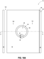
FIGS. 18 and18A ,gate dielectric material 38 is deposited within thevoids 112. Thegate dielectric material 38 may comprise any suitable composition(s); and in some embodiments may comprise, consist essentially of, or consist of silicon dioxide. - Referring to
FIGS. 19 and19A ,gate material 20 andwordline material 114 are formed within the voids 112 (FIG. 18 ). Thegate material 20 andwordline material 114 may comprise any suitable compositions, and may be the same as one another or different from one another. In some embodiments, thegate material 20 may comprise, consist essentially of, or consist of tungsten; and thewordline material 114 may comprise a conductive material to which the tungsten may be selectively etched. For instance, in some embodiments thewordline material 114 may comprise, consist essentially of, or consist of titanium nitride. - The
gate material 20forms transistor gates 16. - The
gate dielectric material 38,semiconductor material 18 andgate material 20 together formtransistor devices first side 106 of theopening 86. Thesemiconductor material 18 comprises thechannel regions 17 extending along thegates 16, and also comprises the source/drain regions 19 and 21 (shown inFIGS. 1 and3 , but not visible inFIGS. 19 and19A ). - Referring to
FIGS. 20 and20A ,insulative material 116 andconductive material 118 are formed within the slit 104 (FIGS. 19 and19A ). Theinsulative material 116 may comprise any suitable composition or combination of compositions; and in some embodiments may comprise, consist essentially of, or consist of one or more of silicon dioxide, silicon nitride, etc. Theinsulative material 116 may be a same composition as theinsulative material 42 in some embodiments. - The
conductive material 118 may comprise any suitable composition(s), such as, for example, one or more of various metals (e.g., titanium, tungsten, cobalt, nickel, platinum, ruthenium, etc.), metal-containing compositions (e.g., metal silicide, metal nitride, metal carbide, etc.), and/or conductively-doped semiconductor materials (e.g., conductively-doped silicon, conductively-doped germanium, etc.). Theconductive material 118 may form wordlines 36a and 36b extending in and out of the page relative to the cross-section ofFIG. 20 . In some embodiments, theconductive material 118 may be a same composition as theconductive material 114, and in other embodiments theconductive materials - A
slit 120 is formed along thesecond side 110 of theopening 86. Theslit 120 extends through the first andsecond levels panel 80. - Referring to
FIGS. 21 and21A ,materials right side 110 of opening 86 to form voids 122. In the illustrated embodiment, thematerial 90 is thinned to leaveliners 124 of thematerial 90 along upper and lower regions of thevoids 122. - Referring to
FIGS. 22 and22A , thefirst electrode material 28 is formed within thevoids 122 and patterned into thefirst electrodes Sacrificial material 126 is provided within thevoids 122 and along theelectrode material 28 to assist in the patterning of theelectrode material 28 into the configuration of thefirst electrodes sacrificial material 126 may comprise any suitable composition(s), and in some embodiments may comprise an oxide formed at sufficiently low temperature such that components associated with circuitry of theassembly 70 are not degraded. - The
voids 122 extend about halfway around theopening 86, and the dashedline 107 is provided to show approximate edges of thevoids 122.FIG. 22B shows a region along one of thelevels 76, and shows theelectrode 22a directly contactingsemiconductor material 18 of thetransistor 12a. The region of thesemiconductor material 18 which contacts theelectrode 22a comprises the first source/drain region 21. - Referring to
FIGS. 23 and23A , the sacrificial material 126 (FIG. 22 ) is removed. Subsequently,capacitor dielectric material 128 is formed along theelectrodes electrode material 30 is formed along thecapacitor dielectric material 128. - The
capacitor dielectric material 128 may comprise any suitable composition(s); such as, for example, one or more of silicon dioxide, silicon nitride, hafnium oxide, zirconium oxide, aluminum oxide, other high-k materials (with high-k meaning a dielectric constant greater than that of silicon dioxide), etc. - The
electrode material 30 formssecond electrodes second electrodes conductive material 30 forms a common conductive plate extending across both of the capacitors. - The
electrodes dielectric material 128 therebetween, form thecapacitor 14a; and theelectrodes dielectric material 128 therebetween, form thecapacitor 14b. - The
transistor 12a and thecapacitor 14a together form adevice 10a along one of thedevice levels 76, and thetransistor 12b and thecapacitor 14b together form adevice 10b along another of thedevice levels 76. Thedevices - In some embodiments, the
opening 86 may be representative of a plurality of openings, as discussed above. In such embodiments, thedevices arrays 50 of the type described above with reference toFIGS. 6 and7 . Each of the memory devices within the memory arrays may be uniquely addressed through a combination of a wordline and a digit line, as discussed above relative to thememory arrays 50 ofFIGS. 6 and7 . - In the embodiment of
FIG. 23 , each device (for instance,device 10a) comprises a transistor (e.g.,transistor 12a) coupled with an associated capacitor (e.g.,capacitor 14a). The capacitor is horizontally offset from the transistor; and both the transistor and the associated capacitor are within asingle device level 76. The devices may be within amemory array 50 of the type described above with reference toFIG. 6 . Wordlines (e.g., wordlines 36a, 36b) extend along thedevice levels 76 and are coupled with gates of thetransistors transistors - In some embodiments, each of the devices (e.g.,
devices FIG. 23 may be considered to be between afirst insulative level 74 below the device, and asecond insulative level 74 above the device. -
FIG. 23 shows theinsulative level 74 abovedevice 10a being labeled as alevel 74a, and shows theinsulative level 74 belowdevice 10a being labeled as level 74b. Thelevel 74a has abottom surface 127, and the level 74b has atop surface 129. The capacitor of thedevice 10a (i.e.,capacitor 14a) has anuppermost surface 131 and alowermost surface 133; and the transistor of thedevice 10a (i.e.,transistor 12a) has anuppermost surface 135 and alowermost surface 137. Theuppermost surfaces transistor 12a and thecapacitor 14a are at about a same elevational level as one another beneath thebottom surface 127 ofupper insulative level 74a; and thelowermost surfaces transistor 12a and thecapacitor 14a are at about a same elevational level as one another above theupper surface 129 of the lower insulative level 74b. - In some embodiments, the
capacitor 14a may have alowermost surface 133 which is at least as far below thelowermost surface 127 of theinsulative level 74a as thelowermost surface 137 of thetransistor 12a, and may have anuppermost surface 131 which is at least as far above theuppermost surface 129 of the insulative level 74b has theuppermost surface 135 of thetransistor 12a. If the top surface of the capacitor is no lower than the top surface of the transistor, and if the bottom surface of the capacitor is also no higher than the bottom surface of the transistor, then thetransistor 12a and thecapacitor 14a may be considered to be in the same planar level as one another (i.e., if the vertical dimension of the transistor is vertically coextensive with the vertical dimension of the capacitor, or vertically sandwiched between the upper and lower surfaces of the capacitor). Alternatively, thetransistor 12a and thecapacitor 14a may be considered to be in the same planar level as one another if the top surface of the transistor is no lower than the top surface of the capacitor, and the bottom surface of the transistor is no higher than the bottom surface of the transistor (i.e., if the vertical dimension of the capacitor is vertically coextensive with the vertical dimension of the transistor, or vertically sandwiched between the upper and lower surfaces of the transistor). - It is to be understood that the invention described herein may be applicable to numerous circuit designs, including, but not limited to memory arrays. Example circuits may include layouts which may have pillars and/or other structures associated, with, for example, transistors, isolation, gates, capacitors, etc. The example circuits may include multiple layers in one or more tier stacks. Example circuits may be one large connected structure, or may be multiple separated structures (e.g., multiple individual thin substrates).
- The structures discussed above may be incorporated into electronic systems. Such electronic systems may be used in, for example, memory modules, device drivers, power modules, communication modems, processor modules, and application-specific modules, and may include multilayer, multichip modules. The electronic systems may be any of a broad range of systems, such as, for example, cameras, wireless devices, displays, chip sets, set top boxes, games, lighting, vehicles, clocks, televisions, cell phones, personal computers, automobiles, industrial control systems, aircraft, etc.
- Unless specified otherwise, the various materials, substances, compositions, etc. described herein may be formed with any suitable methodologies, either now known or yet to be developed, including, for example, atomic layer deposition (ALD), chemical vapor deposition (CVD), physical vapor deposition (PVD), etc.
- The terms "dielectric" and "insulative" may be utilized to describe materials having insulative electrical properties. The terms are considered synonymous in this disclosure. The utilization of the term "dielectric" in some instances, and the term "insulative" (or "electrically insulative") in other instances, may be to provide language variation within this disclosure to simplify antecedent basis within the claims that follow, and is not utilized to indicate any significant chemical or electrical differences.
- The particular orientation of the various embodiments in the drawings is for illustrative purposes only, and the embodiments may be rotated relative to the shown orientations in some applications. The descriptions provided herein, and the claims that follow, pertain to any structures that have the described relationships between various features, regardless of whether the structures are in the particular orientation of the drawings, or are rotated relative to such orientation.
- The cross-sectional views of the accompanying illustrations only show features within the planes of the cross-sections, and do not show materials behind the planes of the cross-sections, unless indicated otherwise, in order to simplify the drawings.
- When a structure is referred to above as being "on" or "against" another structure, it can be directly on the other structure or intervening structures may also be present. In contrast, when a structure is referred to as being "directly on" or "directly against" another structure, there are no intervening structures present.
- Structures (e.g., layers, materials, etc.) may be referred to as "extending vertically" to indicate that the structures generally extend upwardly from an underlying base (e.g., substrate). The vertically-extending structures may extend substantially orthogonally relative to an upper surface of the base, or not.
- Some embodiments include an assembly having a first insulative level over a semiconductor base, a second insulative level over the first insulative level, and a device between the first and second insulative levels. The device has a transistor coupled with a capacitor. The capacitor is horizontally offset relative to the transistor. The capacitor and the transistor are in the same planar level as one another.
- Some embodiments include an assembly having a stack of first and second levels which alternate with one another along a vertical direction. The first levels comprise insulative material and are insulative levels. The second levels comprise integrated devices and are device levels. Each of the integrated devices includes a transistor coupled with a capacitor which is horizontally offset relative to the transistor. The capacitor and the transistor of each of the integrated devices are entirely contained within one of the device levels.
- Some embodiments include an assembly having a stack of first and second levels which alternate with one another along a vertical direction. The first levels have insulative material and are insulative levels. The second levels have integrated devices and are device levels. Each of the integrated devices has a transistor coupled with an associated capacitor which is horizontally offset relative to the transistor. The transistor and the associated capacitor of each of the integrated devices are entirely contained within one of the device levels. The transistors have semiconductor channel material, and have transistor gates along the semiconductor channel material. Each of the transistors has a first source/drain region along one side of the semiconductor channel material and coupled with the associated capacitor, and has a second source/drain region on an opposing side of the semiconductor channel material from the first source/drain region. Wordlines extend horizontally along the device levels and are coupled with the transistor gates. Digit lines extend vertically through the device levels and are coupled with the second source/drain regions of the transistors.
- Some embodiments include a method of forming an integrated structure. An assembly is formed to include a stack of alternating first and second levels. An opening is formed to extend through the stack. Transistor devices are formed within the second levels along a first side of the opening. Each of the transistor devices includes semiconductor material comprising a channel region between a first source/drain region and a second source/drain region. Capacitors are formed within the second levels and along a second side of the opening. Each of the capacitors includes a first electrode, a second electrode, and dielectric material between the first and second electrodes. Each of the second levels comprises one of the capacitors adjacent an associated one of the transistors. The first electrode of said one of the capacitors is directly against the first source/drain region of said associated one of the transistors.
- Further embodiments are set out in the following clauses.
- Clause 1. An assembly comprising: a first insulative level over a semiconductor base; a second insulative level over the first insulative level; and a device between the first and second insulative levels; the device including a transistor coupled with a capacitor; the capacitor being horizontally offset relative to the transistor; the capacitor and the transistor being in a same planar level as one another.
-
Clause 2. The assembly of clause 1 wherein the device is substantially circular along a horizontal cross-section through the device. - Clause 3. The assembly of clause 1 wherein the device is not substantially circular along a horizontal cross-section through the device.
- Clause 4. The assembly of clause 1 wherein the transistor includes a gate proximate a channel material, and wherein the gate brackets a region of the channel material.
- Clause 5. The assembly of clause 1 wherein the transistor includes a gate proximate a channel material, and wherein the gate is either primarily under a region of the channel material or primarily over a region of the channel material.
- Clause 6. An assembly comprising: a stack of first and second levels which alternate with one another along a vertical direction; the first levels comprising insulative material and being insulative levels; the second levels comprising integrated devices and being device levels; each of the integrated devices including a transistor coupled with a capacitor which is horizontally offset relative to the transistor; and the capacitor and the transistor of each of the integrated devices being entirely contained within one of the device levels.
- Clause 7. The assembly of clause 6 wherein each of the transistors comprises a gate and an associated channel material.
- Clause 8. The assembly of clause 7 wherein the gates of at least some of the transistors bracket the associated channel material.
- Clause 9. The assembly of clause 7 wherein the gates of at least some of the transistors do not bracket the associated channel material.
-
Clause 10. The assembly of clause 6 wherein at least one of the integrated devices is substantially circular along a horizontal cross-section through the integrated device. - Clause 11. The assembly of clause 6 wherein at least one of the integrated devices is not substantially circular along a horizontal cross-section through the integrated device.
-
Clause 12. An assembly, comprising: a stack of first and second levels which alternate with one another along a vertical direction; the first levels comprising insulative material and being insulative levels; the second levels comprising integrated devices and being device levels; each of the integrated devices including a transistor coupled with an associated capacitor which is horizontally offset relative to the transistor; the transistor and the associated capacitor of each of the integrated devices being entirely contained within one of the device levels; the transistors comprising semiconductor channel material, and comprising transistor gates along the semiconductor channel material; each of the transistors comprising a first source/drain region along one side of the semiconductor channel material and coupled with the associated capacitor, and comprising a second source/drain region on an opposing side of the semiconductor channel material from said first source/drain region; wordlines extending horizontally along the device levels and being coupled with the transistor gates; and digit lines extending vertically through the device levels and being coupled with the second source/drain regions of the transistors. - Clause 13. The assembly of
clause 12 wherein at least some of the integrated devices within one of the device levels are substantially identical to at least some of the integrated devices within at least one other of the device levels. -
Clause 14. The assembly ofclause 12 wherein all of the integrated devices within one of the device levels are substantially identical to all of the integrated devices within at least one other of the device levels. - Clause 15. The assembly of
clause 12 wherein all of the integrated devices within one of the device levels are substantially identical to all of the integrated devices within all others of the device levels. -
Clause 16. The assembly ofclause 12 wherein at least some of the integrated devices within one of the device levels are not substantially identical to at least some of the integrated devices within another of the device levels. -
Clause 17. The assembly ofclause 16 wherein said at least some of the integrated devices within said one of the device levels differ from said at least some of the integrated devices in said other of the device levels in one or more properties of the semiconductor channel material. -
Clause 18. The assembly ofclause 12 wherein at least one of the digit lines is substantially circular along a horizontal cross-section through said at least one of the digit lines. -
Clause 19. The assembly ofclause 12 wherein at least one of the digit lines is not substantially circular along a horizontal cross-section through said at least one of the digit lines. -
Clause 20. The assembly ofclause 12 wherein at least one of the digit lines is substantially crescent-shaped along a horizontal cross-section through said at least one of the digit lines. -
Clause 21. A method of forming an integrated structure, comprising: forming an assembly to include a stack of alternating first and second levels; forming an opening to extend through the stack; forming transistor devices within the second levels along a first side of the opening; each of the transistor devices including a semiconductor material comprising a channel region between a first source/drain region and a second source/drain region; and forming capacitors within the second levels and along a second side of the opening; each of the capacitors including a first electrode, a second electrode, and a dielectric material between the first and second electrodes; each of the second levels comprising one of the capacitors adjacent an associated one of the transistors; the first electrode of said one of the capacitors being directly against the first source/drain region of said associated one of the transistors. -
Clause 22. The method ofclause 21 wherein the second electrodes of all of the capacitors are coupled to one another. - Clause 23. The method of
clause 21 wherein each of the second levels of the assembly includes a layer of first sacrificial material vertically between a pair of layers of second sacrificial material; wherein the first sacrificial material comprises phosphosilicate glass; wherein a portion of the first sacrificial material of each of the second levels is removed and replaced with the semiconductor material; a remaining portion of the first sacrificial material within each of the second levels being directly against the semiconductor material within each of the second levels; and wherein phosphorus is diffused into the first source/drain region within each of the second levels from the remaining portion of the first sacrificial material within each of the second levels. -
Clause 24. The method of clause 23 further comprising forming a digit line template to extend through the assembly; the digit line template including a vertically-extending region comprising phosphosilicate glass; wherein the phosphosilicate glass of the digit line template is removed and replaced with the semiconductor material as the portion of the first sacrificial material is removed and replaced with the semiconductor material; the semiconductor material which replaces the phosphosilicate glass of the digit line template being at least a portion of a digit line. - Clause 25. The method of
clause 24 further comprising conductively doping the semiconductor material of the digit line and diffusing dopant from the digit line into the second source/drain regions in each of the second levels. - Clause 26. The method of
clause 21 wherein: the opening is a first opening and is one of a plurality of openings formed through the assembly; each of the second levels has the transistor formed along the first side of the first opening and has other transistors formed along first sides of other openings of the plurality of openings; each of the second levels has the capacitor formed along the second side of the first opening and has other capacitors formed along second sides of other openings of the plurality of openings; and wordlines are formed to extend horizontally along the second levels; each of the wordlines along an individual of the second levels being coupled with gates of two or more of the transistors within the individual of the second levels. - Clause 27. The method of clause 26 wherein: individual transistors are coupled with individual capacitors to form memory cells, with each second level comprising a plurality of the memory cells; digit lines are formed extend vertically through the second levels and to be coupled with the second source/drain regions of the transistors; and each of the memory cells is uniquely addressed through a combination of one of the wordlines and one of the digit lines.
Claims (15)
- An assembly comprising:a first insulative level over a semiconductor base;a second insulative level over the first insulative level; anda device between the first and second insulative levels; the device including a transistor coupled with a capacitor; the capacitor being horizontally offset relative to the transistor; the capacitor and the transistor being in a same planar level as one another; wherein the transistor includes a gate proximate a channel region, and wherein the gate brackets the channel region.
- The assembly of claim 1 wherein the device is substantially circular along a horizontal cross-section through the device.
- The assembly of claim 1 wherein the device is not substantially circular along a horizontal cross-section through the device.
- The assembly of claim 1 wherein the gate is either primarily under the channel region or primarily over the channel region.
- The assembly of claim 1, comprising:a stack of first and second levels which alternate with one another along a vertical direction;the first levels comprising insulative material and being insulative levels. the first levels comprising the first insulative level and the second insulative level;the second levels comprising a respective one of the device and being device levels, each of the devices being an integrated device;the capacitor and the transistor of each of the integrated devices being entirely contained within one of the device levels.
- The assembly of claim 5 wherein the gates of at least some of the transistors bracket the associated channel region.
- The assembly of claim 5 wherein the gates of at least some of the transistors do not bracket the associated channel region.
- The assembly of claim 5 wherein at least one of the integrated devices is substantially circular along a horizontal cross-section through the integrated device.
- The assembly of claim 5 wherein at least one of the integrated devices is not substantially circular along a horizontal cross-section through the integrated device.
- The assembly of claim 5 wherein:each of the integrated devices includes a transistor coupled with an associated capacitor which is horizontally offset relative to the transistor; the transistors comprises semiconductor channel material and transistor gates along the semiconductor channel material; each of the transistors comprises a first source/drain region along one side of the semiconductor channel material and coupled with the associated capacitor, and comprises a second source/drain region on an opposing side of the semiconductor channel material from said first source/drain region; andthe assembly further comprises:wordlines extending horizontally along the device levels and being coupled with the transistor gates; anddigit lines extending vertically through the device levels and being coupled with the second source/drain regions of the transistors.
- The assembly of claim 10 wherein at least some of the integrated devices within one of the device levels are substantially identical to at least some of the integrated devices within at least one other of the device levels.
- The assembly of claim 10 wherein at least some of the integrated devices within one of the device levels are not substantially identical to at least some of the integrated devices within another of the device levels.
- The assembly of claim 12 wherein said at least some of the integrated devices within said one of the device levels differ from said at least some of the integrated devices in said other of the device levels in one or more properties of the semiconductor channel material.
- The assembly of claim 10 wherein at least one of the digit lines is substantially circular along a horizontal cross-section through said at least one of the digit lines.
- The assembly of claim 10 wherein at least one of the digit lines is substantially crescent-shaped along a horizontal cross-section through said at least one of the digit lines.
Applications Claiming Priority (3)
| Application Number | Priority Date | Filing Date | Title |
|---|---|---|---|
| US201762595912P | 2017-12-07 | 2017-12-07 | |
| EP18886252.8A EP3682477B1 (en) | 2017-12-07 | 2018-10-04 | Devices having a transistor and a capacitor along a common horizontal level, and methods of forming devices |
| PCT/US2018/054296 WO2019112687A1 (en) | 2017-12-07 | 2018-10-04 | Devices having a transistor and a capacitor along a common horizontal level, and methods of forming devices |
Related Parent Applications (2)
| Application Number | Title | Priority Date | Filing Date |
|---|---|---|---|
| EP18886252.8A Division EP3682477B1 (en) | 2017-12-07 | 2018-10-04 | Devices having a transistor and a capacitor along a common horizontal level, and methods of forming devices |
| EP18886252.8A Division-Into EP3682477B1 (en) | 2017-12-07 | 2018-10-04 | Devices having a transistor and a capacitor along a common horizontal level, and methods of forming devices |
Publications (2)
| Publication Number | Publication Date |
|---|---|
| EP4583659A2 true EP4583659A2 (en) | 2025-07-09 |
| EP4583659A3 EP4583659A3 (en) | 2025-08-13 |
Family
ID=66696350
Family Applications (2)
| Application Number | Title | Priority Date | Filing Date |
|---|---|---|---|
| EP18886252.8A Active EP3682477B1 (en) | 2017-12-07 | 2018-10-04 | Devices having a transistor and a capacitor along a common horizontal level, and methods of forming devices |
| EP25176032.8A Pending EP4583659A3 (en) | 2017-12-07 | 2018-10-04 | Devices having a transistor and a capacitor along a common horizontal level, and methods of forming devices |
Family Applications Before (1)
| Application Number | Title | Priority Date | Filing Date |
|---|---|---|---|
| EP18886252.8A Active EP3682477B1 (en) | 2017-12-07 | 2018-10-04 | Devices having a transistor and a capacitor along a common horizontal level, and methods of forming devices |
Country Status (5)
| Country | Link |
|---|---|
| US (3) | US10707210B2 (en) |
| EP (2) | EP3682477B1 (en) |
| KR (1) | KR102374028B1 (en) |
| CN (1) | CN111095556B (en) |
| WO (1) | WO2019112687A1 (en) |
Families Citing this family (8)
| Publication number | Priority date | Publication date | Assignee | Title |
|---|---|---|---|---|
| KR102932871B1 (en) | 2020-05-10 | 2026-02-27 | 어플라이드 머티어리얼스, 인코포레이티드 | 3d pitch multiplication |
| KR102813959B1 (en) | 2020-09-04 | 2025-05-29 | 에스케이하이닉스 주식회사 | Memory device and method for fabricating the same |
| KR102840953B1 (en) | 2020-10-29 | 2025-07-31 | 에스케이하이닉스 주식회사 | Semiconductor device |
| US11495283B2 (en) * | 2021-01-11 | 2022-11-08 | Micron Technology, Inc. | Integrated assembly with memory array over base, sense amplifiers in base, and vertically-extending digit lines associated with the memory array |
| US12532778B2 (en) * | 2022-05-26 | 2026-01-20 | Micron Technology, Inc. | Microelectronic devices including multiple dies respectively including vertical stacks of memory cells, and related electronic systems |
| JP2024017785A (en) | 2022-07-28 | 2024-02-08 | キオクシア株式会社 | semiconductor storage device |
| US12512135B2 (en) | 2022-10-11 | 2025-12-30 | Samsung Electronics Co., Ltd. | Semiconductor memory device |
| US20240321859A1 (en) * | 2023-03-22 | 2024-09-26 | Intel Corporation | Integrated circuit device with performance-enhancing layout |
Family Cites Families (13)
| Publication number | Priority date | Publication date | Assignee | Title |
|---|---|---|---|---|
| DE10208249B4 (en) | 2002-02-26 | 2006-09-14 | Infineon Technologies Ag | Semiconductor memory with vertical selection transistor |
| DE10260769A1 (en) | 2002-12-23 | 2004-07-15 | Infineon Technologies Ag | Dram semiconductor memory cell production process and cell arrangement has vertical select transistor with upper channel region enclosed by the word line |
| US7326611B2 (en) | 2005-02-03 | 2008-02-05 | Micron Technology, Inc. | DRAM arrays, vertical transistor structures and methods of forming transistor structures and DRAM arrays |
| US7120046B1 (en) * | 2005-05-13 | 2006-10-10 | Micron Technology, Inc. | Memory array with surrounding gate access transistors and capacitors with global and staggered local bit lines |
| KR101717798B1 (en) * | 2009-04-08 | 2017-03-17 | 샌디스크 테크놀로지스 엘엘씨 | Three-dimensional array of re-programmable nonvolatile memory elements having vertical bit lines and a double-global-bit-line architecture |
| JP2012151453A (en) * | 2010-12-28 | 2012-08-09 | Semiconductor Energy Lab Co Ltd | Semiconductor device and driving method of the same |
| US9177872B2 (en) | 2011-09-16 | 2015-11-03 | Micron Technology, Inc. | Memory cells, semiconductor devices, systems including such cells, and methods of fabrication |
| US8748258B2 (en) | 2011-12-12 | 2014-06-10 | International Business Machines Corporation | Method and structure for forming on-chip high quality capacitors with ETSOI transistors |
| KR102101167B1 (en) * | 2012-02-03 | 2020-04-16 | 가부시키가이샤 한도오따이 에네루기 켄큐쇼 | Semiconductor device |
| US8546955B1 (en) * | 2012-08-16 | 2013-10-01 | Xilinx, Inc. | Multi-die stack package |
| WO2018208719A1 (en) * | 2017-05-08 | 2018-11-15 | Micron Technology, Inc. | Memory arrays |
| KR102400951B1 (en) * | 2017-05-08 | 2022-05-23 | 마이크론 테크놀로지, 인크 | Memory arrays |
| KR102524614B1 (en) | 2017-11-24 | 2023-04-24 | 삼성전자주식회사 | Semiconductor memory device |
-
2018
- 2018-10-03 US US16/150,714 patent/US10707210B2/en active Active
- 2018-10-04 EP EP18886252.8A patent/EP3682477B1/en active Active
- 2018-10-04 CN CN201880060496.8A patent/CN111095556B/en active Active
- 2018-10-04 EP EP25176032.8A patent/EP4583659A3/en active Pending
- 2018-10-04 KR KR1020207013276A patent/KR102374028B1/en active Active
- 2018-10-04 WO PCT/US2018/054296 patent/WO2019112687A1/en not_active Ceased
-
2020
- 2020-05-29 US US16/887,338 patent/US11081487B2/en active Active
-
2021
- 2021-07-16 US US17/378,043 patent/US11626406B2/en active Active
Also Published As
| Publication number | Publication date |
|---|---|
| WO2019112687A1 (en) | 2019-06-13 |
| KR102374028B1 (en) | 2022-03-14 |
| KR20200055800A (en) | 2020-05-21 |
| US20190181142A1 (en) | 2019-06-13 |
| CN111095556B (en) | 2023-10-20 |
| US11626406B2 (en) | 2023-04-11 |
| CN111095556A (en) | 2020-05-01 |
| US20210343719A1 (en) | 2021-11-04 |
| EP3682477A4 (en) | 2020-10-21 |
| EP4583659A3 (en) | 2025-08-13 |
| US10707210B2 (en) | 2020-07-07 |
| EP3682477A1 (en) | 2020-07-22 |
| US11081487B2 (en) | 2021-08-03 |
| EP3682477B1 (en) | 2025-07-16 |
| US20200295007A1 (en) | 2020-09-17 |
Similar Documents
| Publication | Publication Date | Title |
|---|---|---|
| US11081487B2 (en) | Devices having a transistor and a capacitor along a common horizontal level, and methods of forming devices | |
| US11706909B2 (en) | Integrated assemblies comprising memory cells and shielding material between the memory cells | |
| EP3840046B1 (en) | Memory cells and memory arrays | |
| CN112185961B (en) | Integrated assembly and method of forming an integrated assembly | |
| US11244952B2 (en) | Array of capacitors, array of memory cells, methods of forming an array of capacitors, and methods of forming an array of memory cells | |
| CN100485938C (en) | Semiconductor constructions having a buried bit line, and method of forming same | |
| US10580776B2 (en) | Memory arrays | |
| US10290422B1 (en) | Capacitors and integrated assemblies which include capacitors | |
| US11239242B2 (en) | Integrated assemblies having dielectric regions along conductive structures, and methods of forming integrated assemblies | |
| US10790288B2 (en) | Memory arrays comprising ferroelectric capacitors | |
| KR102744169B1 (en) | An integrated assembly having conductive material along three of four sides around an active region, and a method for forming the integrated assembly | |
| US20240224495A1 (en) | Semiconductor device and method for fabricating the same | |
| US20180294268A1 (en) | Apparatuses Containing FinFETS | |
| US11710513B2 (en) | Integrated assemblies having ferroelectric transistors and methods of forming integrated assemblies | |
| US20250301624A1 (en) | Memory Circuitry And Methods Used In Forming Memory Circuitry | |
| US20240292605A1 (en) | Semiconductor device and method for fabricating the same |
Legal Events
| Date | Code | Title | Description |
|---|---|---|---|
| PUAI | Public reference made under article 153(3) epc to a published international application that has entered the european phase |
Free format text: ORIGINAL CODE: 0009012 |
|
| STAA | Information on the status of an ep patent application or granted ep patent |
Free format text: STATUS: REQUEST FOR EXAMINATION WAS MADE |
|
| 17P | Request for examination filed |
Effective date: 20250513 |
|
| AC | Divisional application: reference to earlier application |
Ref document number: 3682477 Country of ref document: EP Kind code of ref document: P |
|
| AK | Designated contracting states |
Kind code of ref document: A2 Designated state(s): AL AT BE BG CH CY CZ DE DK EE ES FI FR GB GR HR HU IE IS IT LI LT LU LV MC MK MT NL NO PL PT RO RS SE SI SK SM TR |
|
| PUAL | Search report despatched |
Free format text: ORIGINAL CODE: 0009013 |
|
| AK | Designated contracting states |
Kind code of ref document: A3 Designated state(s): AL AT BE BG CH CY CZ DE DK EE ES FI FR GB GR HR HU IE IS IT LI LT LU LV MC MK MT NL NO PL PT RO RS SE SI SK SM TR |
|
| RIC1 | Information provided on ipc code assigned before grant |
Ipc: H10B 12/00 20230101AFI20250709BHEP |