EP4583359A1 - Method and apparatus for setting battery pack identifier - Google Patents
Method and apparatus for setting battery pack identifier Download PDFInfo
- Publication number
- EP4583359A1 EP4583359A1 EP24215488.8A EP24215488A EP4583359A1 EP 4583359 A1 EP4583359 A1 EP 4583359A1 EP 24215488 A EP24215488 A EP 24215488A EP 4583359 A1 EP4583359 A1 EP 4583359A1
- Authority
- EP
- European Patent Office
- Prior art keywords
- voltage
- pin
- battery pack
- identifier
- input
- Prior art date
- Legal status (The legal status is an assumption and is not a legal conclusion. Google has not performed a legal analysis and makes no representation as to the accuracy of the status listed.)
- Pending
Links
Images


Classifications
-
- H—ELECTRICITY
- H02—GENERATION; CONVERSION OR DISTRIBUTION OF ELECTRIC POWER
- H02J—ELECTRIC POWER NETWORKS; CIRCUIT ARRANGEMENTS OR SYSTEMS FOR SUPPLYING OR DISTRIBUTING ELECTRIC POWER; SYSTEMS FOR STORING ELECTRIC ENERGY
- H02J7/00—Circuit arrangements for charging or discharging batteries or for supplying loads from batteries
- H02J7/50—Circuit arrangements for charging or discharging batteries or for supplying loads from batteries acting upon multiple batteries simultaneously or sequentially
-
- H—ELECTRICITY
- H01—ELECTRIC ELEMENTS
- H01M—PROCESSES OR MEANS, e.g. BATTERIES, FOR THE DIRECT CONVERSION OF CHEMICAL ENERGY INTO ELECTRICAL ENERGY
- H01M10/00—Secondary cells; Manufacture thereof
- H01M10/42—Methods or arrangements for servicing or maintenance of secondary cells or secondary half-cells
- H01M10/425—Structural combination with electronic components, e.g. electronic circuits integrated to the outside of the casing
-
- H—ELECTRICITY
- H02—GENERATION; CONVERSION OR DISTRIBUTION OF ELECTRIC POWER
- H02J—ELECTRIC POWER NETWORKS; CIRCUIT ARRANGEMENTS OR SYSTEMS FOR SUPPLYING OR DISTRIBUTING ELECTRIC POWER; SYSTEMS FOR STORING ELECTRIC ENERGY
- H02J7/00—Circuit arrangements for charging or discharging batteries or for supplying loads from batteries
- H02J7/485—Circuit arrangements for charging or discharging batteries or for supplying loads from batteries with provisions for charging different types of batteries
-
- H—ELECTRICITY
- H02—GENERATION; CONVERSION OR DISTRIBUTION OF ELECTRIC POWER
- H02J—ELECTRIC POWER NETWORKS; CIRCUIT ARRANGEMENTS OR SYSTEMS FOR SUPPLYING OR DISTRIBUTING ELECTRIC POWER; SYSTEMS FOR STORING ELECTRIC ENERGY
- H02J7/00—Circuit arrangements for charging or discharging batteries or for supplying loads from batteries
- H02J7/40—Circuit arrangements for charging or discharging batteries or for supplying loads from batteries characterised by the exchange of charge or discharge related data
- H02J7/443—Circuit arrangements for charging or discharging batteries or for supplying loads from batteries characterised by the exchange of charge or discharge related data using passive battery identification means, e.g. resistors or capacitors
-
- B—PERFORMING OPERATIONS; TRANSPORTING
- B60—VEHICLES IN GENERAL
- B60L—PROPULSION OF ELECTRICALLY-PROPELLED VEHICLES; SUPPLYING ELECTRIC POWER FOR AUXILIARY EQUIPMENT OF ELECTRICALLY-PROPELLED VEHICLES; ELECTRODYNAMIC BRAKE SYSTEMS FOR VEHICLES IN GENERAL; MAGNETIC SUSPENSION OR LEVITATION FOR VEHICLES; MONITORING OPERATING VARIABLES OF ELECTRICALLY-PROPELLED VEHICLES; ELECTRIC SAFETY DEVICES FOR ELECTRICALLY-PROPELLED VEHICLES
- B60L58/00—Methods or circuit arrangements for monitoring or controlling batteries or fuel cells, specially adapted for electric vehicles
- B60L58/10—Methods or circuit arrangements for monitoring or controlling batteries or fuel cells, specially adapted for electric vehicles for monitoring or controlling batteries
- B60L58/18—Methods or circuit arrangements for monitoring or controlling batteries or fuel cells, specially adapted for electric vehicles for monitoring or controlling batteries of two or more battery modules
-
- G—PHYSICS
- G01—MEASURING; TESTING
- G01R—MEASURING ELECTRIC VARIABLES; MEASURING MAGNETIC VARIABLES
- G01R31/00—Arrangements for testing electric properties; Arrangements for locating electric faults; Arrangements for electrical testing characterised by what is being tested not provided for elsewhere
- G01R31/50—Testing of electric apparatus, lines, cables or components for short-circuits, continuity, leakage current or incorrect line connections
-
- H—ELECTRICITY
- H01—ELECTRIC ELEMENTS
- H01M—PROCESSES OR MEANS, e.g. BATTERIES, FOR THE DIRECT CONVERSION OF CHEMICAL ENERGY INTO ELECTRICAL ENERGY
- H01M10/00—Secondary cells; Manufacture thereof
- H01M10/42—Methods or arrangements for servicing or maintenance of secondary cells or secondary half-cells
- H01M10/48—Accumulators combined with arrangements for measuring, testing or indicating the condition of cells, e.g. the level or density of the electrolyte
- H01M10/482—Accumulators combined with arrangements for measuring, testing or indicating the condition of cells, e.g. the level or density of the electrolyte for several batteries or cells simultaneously or sequentially
-
- H—ELECTRICITY
- H02—GENERATION; CONVERSION OR DISTRIBUTION OF ELECTRIC POWER
- H02J—ELECTRIC POWER NETWORKS; CIRCUIT ARRANGEMENTS OR SYSTEMS FOR SUPPLYING OR DISTRIBUTING ELECTRIC POWER; SYSTEMS FOR STORING ELECTRIC ENERGY
- H02J7/00—Circuit arrangements for charging or discharging batteries or for supplying loads from batteries
- H02J7/40—Circuit arrangements for charging or discharging batteries or for supplying loads from batteries characterised by the exchange of charge or discharge related data
- H02J7/47—Arrangements for checking compatibility or authentication between one component, e.g. a battery or a battery charger, and another component, e.g. a power source
-
- H—ELECTRICITY
- H03—ELECTRONIC CIRCUITRY
- H03M—CODING; DECODING; CODE CONVERSION IN GENERAL
- H03M1/00—Analogue/digital conversion; Digital/analogue conversion
- H03M1/12—Analogue/digital converters
-
- H—ELECTRICITY
- H01—ELECTRIC ELEMENTS
- H01M—PROCESSES OR MEANS, e.g. BATTERIES, FOR THE DIRECT CONVERSION OF CHEMICAL ENERGY INTO ELECTRICAL ENERGY
- H01M10/00—Secondary cells; Manufacture thereof
- H01M10/42—Methods or arrangements for servicing or maintenance of secondary cells or secondary half-cells
- H01M10/4221—Methods or arrangements for servicing or maintenance of secondary cells or secondary half-cells with battery type recognition
-
- H—ELECTRICITY
- H01—ELECTRIC ELEMENTS
- H01M—PROCESSES OR MEANS, e.g. BATTERIES, FOR THE DIRECT CONVERSION OF CHEMICAL ENERGY INTO ELECTRICAL ENERGY
- H01M10/00—Secondary cells; Manufacture thereof
- H01M10/42—Methods or arrangements for servicing or maintenance of secondary cells or secondary half-cells
- H01M10/425—Structural combination with electronic components, e.g. electronic circuits integrated to the outside of the casing
- H01M2010/4278—Systems for data transfer from batteries, e.g. transfer of battery parameters to a controller, data transferred between battery controller and main controller
-
- H—ELECTRICITY
- H01—ELECTRIC ELEMENTS
- H01M—PROCESSES OR MEANS, e.g. BATTERIES, FOR THE DIRECT CONVERSION OF CHEMICAL ENERGY INTO ELECTRICAL ENERGY
- H01M2220/00—Batteries for particular applications
- H01M2220/20—Batteries in motive systems, e.g. vehicle, ship, plane
Definitions
- This disclosure relates to a method and apparatus for setting a battery pack identifier.
- Electric vehicles mainly use battery device as a power source to drive motors.
- battery device As battery device with high output and large charging capacity is desired, battery device in which a plurality of battery packs is connected in parallel are being used.
- different hardware may be provided to the plurality of battery packs for identification of the plurality of battery packs.
- costs may be increased by producing different versions of hardware.
- Another method is to allocate an identifier to each battery pack in software.
- software development complexity may be increased.
- the present invention provides a method and apparatus for setting a battery pack identifier that sets the identifier of each of a plurality of battery packs using the same hardware.
- a battery pack identifier that sets the identifier of each of a plurality of battery packs using the same hardware.
- it is possible to set a battery pack identifier without providing different hardware for each battery pack to set the battery pack identifier.
- software processing for setting the battery pack identifier may not be necessary.
- an apparatus for setting a battery pack identifier of a battery pack includes, a first supply configured to supply a power source voltage through a first pin; a second supply configured to supply a ground voltage through a second pin; a plurality of analog-to-digital converters configured to have an input pin and an output pin, and configured to transmit a voltage corresponding to a voltage input through the input pin to the output pin; a plurality of jumper wiring configured to connect input pins of the plurality of analog-to-digital converters with the first pin or the second pin, respectively; and a controller configured to set the battery pack identifier of the battery pack based on the voltages received through the output pin of each of the plurality of analog-to-digital converters.
- the apparatus according to the first aspect may further comprise: a pull-up voltage supply comprising the first pin and a resistor R1.
- the input pin may be connected to the first pin or the second pin through the jumper wiring.
- Each of the plurality of analog-to-digital converters may include, a voltage divider circuit comprising a plurality of first resistors connected between the input pin and a ground, and configured to provide a voltage divided by the plurality of first resistors to the output pin.
- the voltage divider circuit may further include, a second resistor connected between a power source supplying the power source voltage and the input pin.
- the controller may be configured to detect disconnection of the plurality of jumper wiring based on the voltages received through the output pin of the plurality of analog-to-digital converters. Thus, it is possible to detect defects such as non-connection or disconnection of the jumper wiring through the voltage received through the output pin 2422 of the analog-to-digital converters.
- the controller may be configured to determine the value of each bit of the battery pack identifier based on the voltage received through the output pin of each of the plurality of analog-to-digital converters.
- the controller may be configured to set the value of a corresponding bit to a first value, and if the voltage received through the output pin is greater than the ground voltage, may be configured to set the value of the corresponding bit to a second value different from the first value
- a method for setting an identifier of a battery pack in an apparatus for setting a battery pack identifier includes, converting, by each of a plurality of analog-to-digital converters, a voltage input through an input pin into a first voltage; and setting an identifier of the battery pack based on the first voltage converted by each of the plurality of analog-to-digital converters.
- a power source voltage or a ground voltage may be supplied to each input pin of the plurality of analog-to-digital converters according to external control.
- the input pins of the plurality of analog-to-digital converters may be connected to a first pin supplying the power source voltage or a second pin supplying the ground voltage through a plurality of jumper wiring, respectively.
- the converting may include dividing the input voltage by a plurality of first resistors connected between the input pin and a ground.
- the setting an identifier of the battery pack may include determining the value of each bit of the identifier based on the first voltage converted by each of the plurality of analog-to-digital converters.
- the determining the value of each bit of the identifier may include, if the first voltage is the ground voltage, setting the value of a corresponding bit to a first value; and if the first voltage is greater than the ground voltage, setting the value of a corresponding bit to a second value different from the first value.
- a component in addition, if a component is referred to be "connected” with another component, it includes not only the case where two components are “directly connected” but also the case where two components are “indirectly or non-contactedly connected” with another component interposed therebetween, or the case where two components are “electrically connected.” On the other hand, if an element is referred to as “directly connected” to another element, it should be understood that no other element exists in the middle.
- the plurality of battery packs 110, 120, and 130 may be connected to the MBMS 140.
- the plurality of battery packs 110, 120, and 130 may be connected to the MBMS 140 through wiring.
- Each of the plurality of battery packs 110, 120, and 130 may set a battery pack identifier based on a control signal input from the outside and provide the set battery pack identifier to the MBMS 140.
- the MBMS 140 may control the battery packs 110, 120, and 130 using the battery pack identifiers of the battery packs 110, 120, and 130. As one example, the MBMS 140 may control charging or discharging of the battery packs 110, 120, and 130 using the battery pack identifiers of the battery packs 110, 120, and 130.
- the battery system 100 may have a structure that may be connected to an external device. If the external device is a load, the battery system 100 may be discharged by operating as a power source that supplies power to the load.
- the external device that operates as the load may be, for example, an electronic device, a transportation device, or an energy storage system (ESS), and the transportation device may be a vehicle such as an electric vehicle or a hybrid vehicle.
- ESS energy storage system
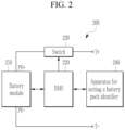
- FIG. 2 is a diagram illustrating an example of the battery pack shown in FIG. 1 .
- the battery pack 200 includes at least one battery module 210, a BMS 220, a switch 230, and an apparatus for setting a battery pack identifier 240.
- the battery pack 200 may be the battery pack 110, 120, or 130 shown in FIG. 1 .
- the battery pack 200 may be connected to an external device through terminals T+ and T-. If the external device is a charging device, the battery pack 200 may be charged by the charging device. If the external device is a load, the battery pack 200 may be discharged by the load.
- the at least one battery module 210 may include a plurality of cells electrically connected to each other in series and/or parallel.
- the battery module 210 may include a positive terminal PV+ and a negative terminal PV-.
- the switch 230 may be connected between the positive terminal PV+ of the battery module 210 and the terminal T+ of the battery pack 200, and may control the current path during charging and discharging of the battery module 210. Closing and opening of the switch 230 may be controlled according to a switch control signal supplied from the BMS 220.
- the BMS 220 may control and manage the overall operation of the battery pack 200.
- the BMS 220 may collect the overall status information of the battery module 210 and the cells included in the battery module 210, and monitor the overall status of the battery module 210 and the cells included in the battery module 210.
- BMS 220 may measure or collect cell data sensed by each cell.
- cell data may include voltage data of a cell.
- BMS 220 may collect data sensed by battery module 210.
- such data may include data regarding the current or temperature of the battery module 210.
- the BMS 220 may perform various control functions to adjust the state of the battery module 210 and the cells included in the battery module 210 based on the status information of the battery module 210 and the cells included in the battery module 210.
- the BMS 220 may control the charging and discharging current of the battery module 210 based on information such as a plurality of cell voltages and battery currents, and perform a cell balancing operation for a plurality of cells.
- the BMS 220 may transmit the collected data to the MBMS (140 in FIG. 1 ).
- the MBMS (140 in FIG. 1 ) can store and manage data collected from the BMS 220 of the battery pack 200 and control the battery pack 200 based on the collected data.
- the MBMS (140 in FIG. 1 ) may collect data from a plurality of battery packs 110, 120, and 130 as shown in FIG. 1 , and may control the plurality of battery packs 110, 120, and 130 based on the collected data. Therefore, a battery pack identifier is desired to distinguish each battery pack 110, 120, and 130.
- the apparatus for setting a battery pack identifier 240 may set the battery pack identifier according to external control.
- the apparatus for setting a battery pack identifier 240 may transmit the battery pack identifier to the BMS 220.
- the BMS 220 may transmit the collected data along with the battery pack identifier to the MBMS (140 in FIG. 1 ).
- the MBMS (140 in FIG. 1 ) may store and manage received data in response to the battery pack identifier and control the battery pack 200 using the battery pack identifier.
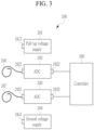
- FIG. 3 is a diagram showing an apparatus for setting a battery pack identifier according to an embodiment
- FIG. 4 is a circuit diagram of the pull-up voltage supply, ADC, and ground voltage supply shown in FIG. 3 .
- the apparatus for setting a battery pack identifier 240 may include a pull-up voltage supply 241, a plurality of analog to digital converters (ADCs) 242 and 243, a ground voltage supply 244, and a controller 245.
- the apparatus for setting a battery pack identifier 240 may further include jumper wirings 246 and 247.
- the pull-up voltage supply 241 may supply a pull-up voltage Vpu1 from a pull-up power source.
- the pull-up power source may refer to a power source that supplies a power supply voltage.
- the pull-up voltage supply 241 may include a pull-up power source pin 2411 and a resistor R1.
- the resistor R1 may be connected between the pull-up power source and the pull-up power source pin 2411, and the pull-up power source pin 2411 may supply the pull-up voltage Vpu1 to the outside.
- the ground voltage supply 244 may supply a ground voltage.
- the ground voltage supply 244 may include a ground pin 2441 for outputting the ground voltage to the outside.
- the ground pin 2441 may be connected to a ground.
- the input pin 2421 may be connected to the pull-up power source pin 2411 or the ground pin 2441 through the jumper wiring 246. If the input pin 2421 is connected to the pull-up power source pin 2411, the pull-up voltage Vpu1 may be supplied to the input pin 2421 through the pull-up voltage supply 241. The pull-up voltage Vpu1 supplied from the pull-up voltage supply 241 may be divided by the resistors R1, R2, R3, and R4, and the divided voltage may be transmitted to the output pin 2422. At this time, the divided voltage may be a voltage greater than 0V. If the input pin 2421 is connected to the ground pin 2441, the voltage of the input pin 2421 may be 0V, and 0V may be transmitted to the output pin 2422.
- the ADC 243 may include an input pin 2431, an output pin 2432, and resistors R5, R6, and R7.
- the resistance values of the resistors R5, R6, and R7 may be the same as the resistance values of the resistors R2, R3, and R4, respectively.
- the resistor R5 may be connected between the input pin 2431 and the output pin 2432.
- the output pin 2432 may be connected to the controller 245 through wiring.
- the resistor R6 may be connected between the output pin 2432 and the ground.
- the resistor R7 may be connected between the input pin 2431 and a pull-up power source that supplies the pull-up voltage Vpu1.
- the resistors R5, R6, and R7 may divide the voltage of the input pin 2431 and provide the divided voltage to the output pin 2432.
- the resistors R5, R6, and R7 may be a voltage divider circuit.
- the resistance values of the resistors R5, R6, and R7 may be different from the resistance values of the resistors R2, R3, and R4, respectively. In this case, the voltage output through the output pin 2422 and the voltage output through the output pin 2432 will be different.
- the input pin 2431 may be connected to the pull-up power source pin 2411 or the ground pin 2441 through a jumper wiring 247.
- the voltage of the input pin 2431 may be the pull-up voltage Vpu1
- the pull-up voltage Vpu1 may be divided by the resistors R1, R7, R5 and R6, and the divided voltage may be transmitted to the output pin 2432.
- the divided voltage may be a voltage greater than 0V.
- the voltage of the input pin 2431 may be 0V, and 0V may be transmitted to the output pin 2432.
- the controller 245 may set the battery pack identifier of the battery pack 200 based on information transmitted through the output pins 2422 and 2432 of the ADCs 242 and 243.
- the controller 245 may detect disconnection of the jumper wirings 246 and 247 to input pins 2421 and 2431 of ADCs 242, based on information transmitted through the output pins 2422 and 2432 of the ADCs 242 and 243. That is, the controller 245 may detect whether the jumper wirings 246 and 247 are not connected to the input pins 2421 and 2431.
- the disconnection of the jumper wirings 246 and 247 may mean that no voltage is input to the input pins 2421 and 2431 of the ADCs 242 and 243. For example, if the jumper wiring 246 is not connected to the input pin 2421 of the ADC 242, no voltage may be input to the input pin 2421 of the ADC 242.
- the pull-up voltage Vpu1 supplied inside the ADC 242 may be divided by the resistors R2, R3, and R4. Meanwhile, if the pull-up voltage Vpu1 is input through the connection of the jumper wiring 246 to the input pin 2421 of the ADC 242, the pull-up voltage Vpu1 may be divided by the resistors R1, R4, R2, and R3. The voltage divided by the resistors R1, R4, R2, and R3 is different from the voltage divided by the resistors R2, R3, and R4.
- VOUT 1 Vpu 1 ⁇ R 3 R 1 / / R 4 + R 2 + R 3
- Equation 1 (R1//R4) may represent the total resistance value of the resistor R1 and resistor R4 connected in parallel.
- VOUT2 Vpu 1 ⁇ R 3 R 4 + R 2 + R 3
- the controller 245 may detect defects such as non-connection or disconnection of the jumper wiring 246 through the voltage received through the output pin 2422 of the ADC 242.
- FIG. 5 to 8 are diagrams illustrating an example of a method for determining a battery pack identifier in an apparatus for setting a battery pack identifier.
- the input pin 2421 of the ADC 242 may be connected to the ground pin 2441 through the jumper wiring 246, and the input pin 2431 of the ADC 243 may be connected to the ground pin 2441 through the jumper wiring 247.
- the controller 245 may receive 0V from output pin 2422 of ADC 242, and may receive 0V from output pin 2432 of ADC 243, and may determine the battery pack identifier of battery pack 200 as "00".
- the input pin 2421 of the ADC 242 may be connected to the pull-up power source pin 2411 through the jumper wiring 246, and the input pin 2431 of the ADC 243 may be connected to the ground pin 2441 through the jumper wiring 247.
- the controller 245 may receive V1 voltage from output pin 2422 of ADC 242, may receive 0V from output pin 2432 of ADC 243, and may determine the battery pack identifier of battery pack 200 as "10".
- V1 voltage may represent the divided voltage of the resistors R1, R4, R2, and R3 with respect to the pull-up voltage Vpu1.
- the input pin 2421 of the ADC 242 may be connected to the ground pin 2441 through the jumper wiring 246, and the input pin 2431 of the ADC 243 may be connected to the pull-up power source pin 2441 through the jumper wiring 247.
- controller 245 may receive 0V from output pin 2422 of ADC 242, may receive V1 voltage from output pin 2432 of ADC 243, and may determine the battery pack identifier of battery pack 200 as "01".
- the input pin 2421 of the ADC 242 may be connected to the pull-up power source pin 2411 through the jumper wiring 246, and the input pin 2431 of the ADC 243 may be connected to the pull-up power source pin 2411 through the jumper wiring 247.
- controller 245 may receive V1 voltage from output pin 2422 of ADC 242, may receive V1 voltage from output pin 2432 of ADC 243, and may determine the battery pack identifier of battery pack 200 as "11".
- the controller 245 may determine the battery pack identifier by allocating a bit value of 1 in response to the V1 voltage and a bit value of 0 in response to 0V, as shown in FIGS. 5 to 8 .
- the controller 245 may determine the battery pack identifier by allocating a bit value of 0 in response to V1 voltage and a bit value of 1 in response to 0V. For example, if the controller 245 receives V1 voltage from the output pin 2422 of ADC 242 and receives 0V from the output pin 2432 of ADC 243, the battery pack identifier of this battery pack 200 may be determined as "01".
- the input pins of the ADCs 242 and 243 may be selectively connected to the pull-up power source pin 2411 or the ground pin 2441 using the jumper wirings 246 and 247, so that the battery pack identifier of the battery pack 200 may be set by the apparatus for setting a battery pack identifier 240 according to the embodiment. Accordingly, the apparatus for setting a battery pack identifier 240 does not desired to provide different hardware for each battery pack to set the battery pack identifier, and may not desired software processing.
- the battery pack identifier of the battery pack 200 consists of 2 bits. That is, pack identifiers may be allocated to four battery packs in the battery system 100. As the number of battery packs in the battery system 100 increases, it may be possible to allocate battery pack identifiers to the battery packs by increasing the number of ADCs.
- the apparatus for setting a battery pack identifier 240 may include a plurality of ADCs. At this time, some of the plurality of ADCs may be used to allocate battery pack identifiers, and the remaining ADCs may be used in connection with at least one sensor.
- the sensor may be, for example, a temperature sensor or a current sensor.
Landscapes
- Engineering & Computer Science (AREA)
- Power Engineering (AREA)
- Manufacturing & Machinery (AREA)
- Chemical & Material Sciences (AREA)
- Chemical Kinetics & Catalysis (AREA)
- Electrochemistry (AREA)
- General Chemical & Material Sciences (AREA)
- Microelectronics & Electronic Packaging (AREA)
- Life Sciences & Earth Sciences (AREA)
- Sustainable Development (AREA)
- Sustainable Energy (AREA)
- Transportation (AREA)
- Mechanical Engineering (AREA)
- Theoretical Computer Science (AREA)
- Physics & Mathematics (AREA)
- General Physics & Mathematics (AREA)
- Charge And Discharge Circuits For Batteries Or The Like (AREA)
Abstract
A method and apparatus for setting a battery pack identifier may be provided. The apparatus for setting a battery pack identifier of a battery pack may include, a first supply configured to supply a power source voltage through a first pin; a second supply configured to supply a ground voltage through a second pin; a plurality of analog-to-digital converters configured to have an input pin and an output pin, and configured to transmit a voltage corresponding to a voltage input through the input pin to the output pin; a plurality of jumper wiring configured to connect input pins of the plurality of analog-to-digital converters with the first pin or the second pin, respectively; and a controller configured to set the battery pack identifier of the battery pack based on the voltages received through the output pin of each of the plurality of analog-to-digital converters.
Description
- This disclosure relates to a method and apparatus for setting a battery pack identifier.
- Electric vehicles (EVs) mainly use battery device as a power source to drive motors. As battery device with high output and large charging capacity is desired, battery device in which a plurality of battery packs is connected in parallel are being used.
- In this way, as the plurality of battery packs are used, identification of the plurality of battery packs is desired.
- In one method, different hardware may be provided to the plurality of battery packs for identification of the plurality of battery packs. However, in case of this method, costs may be increased by producing different versions of hardware.
- Another method is to allocate an identifier to each battery pack in software. However, in case of this method, software development complexity may be increased.
- The present invention is set out in the appended set of claims, wherein the drawings and respective description relate to advantageous embodiments thereof.
- The present invention provides a method and apparatus for setting a battery pack identifier that sets the identifier of each of a plurality of battery packs using the same hardware. Thus, it is possible to set a battery pack identifier without providing different hardware for each battery pack to set the battery pack identifier. In addition, software processing for setting the battery pack identifier may not be necessary.
- According to a first aspect of the present invention, an apparatus for setting a battery pack identifier of a battery pack is provided. The apparatus for setting a battery pack identifier of a battery pack includes, a first supply configured to supply a power source voltage through a first pin; a second supply configured to supply a ground voltage through a second pin; a plurality of analog-to-digital converters configured to have an input pin and an output pin, and configured to transmit a voltage corresponding to a voltage input through the input pin to the output pin; a plurality of jumper wiring configured to connect input pins of the plurality of analog-to-digital converters with the first pin or the second pin, respectively; and a controller configured to set the battery pack identifier of the battery pack based on the voltages received through the output pin of each of the plurality of analog-to-digital converters.
- The apparatus according to the first aspect may further comprise: a pull-up voltage supply comprising the first pin and a resistor R1.
- The input pin may be connected to the first pin or the second pin through the jumper wiring.
- Each of the plurality of analog-to-digital converters may include, a voltage divider circuit comprising a plurality of first resistors connected between the input pin and a ground, and configured to provide a voltage divided by the plurality of first resistors to the output pin.
- The voltage divider circuit may further include, a second resistor connected between a power source supplying the power source voltage and the input pin.
- The controller may be configured to detect disconnection of the plurality of jumper wiring based on the voltages received through the output pin of the plurality of analog-to-digital converters. Thus, it is possible to detect defects such as non-connection or disconnection of the jumper wiring through the voltage received through the
output pin 2422 of the analog-to-digital converters. - The controller may be configured to determine the value of each bit of the battery pack identifier based on the voltage received through the output pin of each of the plurality of analog-to-digital converters.
- If the voltage received through the output pin is the ground voltage, the controller may be configured to set the value of a corresponding bit to a first value, and if the voltage received through the output pin is greater than the ground voltage, may be configured to set the value of the corresponding bit to a second value different from the first value
- According to another aspect of the present invention, a method for setting an identifier of a battery pack in an apparatus for setting a battery pack identifier is provided. The method for setting an identifier of a battery pack includes, converting, by each of a plurality of analog-to-digital converters, a voltage input through an input pin into a first voltage; and setting an identifier of the battery pack based on the first voltage converted by each of the plurality of analog-to-digital converters.
- A power source voltage or a ground voltage may be supplied to each input pin of the plurality of analog-to-digital converters according to external control.
- The input pins of the plurality of analog-to-digital converters may be connected to a first pin supplying the power source voltage or a second pin supplying the ground voltage through a plurality of jumper wiring, respectively.
- The converting may include dividing the input voltage by a plurality of first resistors connected between the input pin and a ground.
- The setting an identifier of the battery pack may include determining the value of each bit of the identifier based on the first voltage converted by each of the plurality of analog-to-digital converters.
- The determining the value of each bit of the identifier may include, if the first voltage is the ground voltage, setting the value of a corresponding bit to a first value; and if the first voltage is greater than the ground voltage, setting the value of a corresponding bit to a second value different from the first value.
- A third aspect of the present invention is a battery pack comprising at least one battery module, a battery management system, BMS, a switch, and
the apparatus according to the first aspect. -
-
FIG. 1 is a diagram showing an example of a battery system according to an embodiment. -
FIG. 2 is a diagram illustrating an example of the battery pack shown inFIG. 1 . -
FIG. 3 is a diagram showing an apparatus for setting a battery pack identifier according to an embodiment. -
FIG. 4 is a circuit diagram of the pull-up voltage supply, ADC, and ground voltage supply shown inFIG. 3 . -
FIG. 5 to 8 are diagrams illustrating an example of a method for determining a battery pack identifier in an apparatus for setting a battery pack identifier. - Example embodiments will now be described more fully hereinafter with reference to the accompanying drawings; however, they may be embodied in different forms and should not be construed as limited to the embodiments set forth herein. Rather, these embodiments are provided so that this disclosure will be thorough and complete, and will fully convey exemplary implementations to those skilled in the art. The drawings and description are to be regarded as illustrative in nature and not restrictive. Like reference numerals designate like elements throughout the specification. In the flowchart described with reference to the drawings in this specification, the order of operations may be changed, several operations may be merged, some operations may be divided, and specific operations may not be performed.
- Throughout the specification and claims, if a part is referred to "include" a certain element, it may mean that it may further include other elements rather than exclude other elements, unless specifically indicated otherwise.
- In addition, expressions described in the singular may be interpreted in the singular or plural unless explicit expressions such as "one" or "single" are used.
- Furthermore, terms including an ordinal number, such as first, second, etc., may be used to describe various elements, but the elements are not limited by the terms. The above terms are used only for the purpose of distinguishing one element from another element. For example, without departing from the scope of the present disclosure, a first element may be referred to as a second element, and similarly, a second element may be referred to as a first element.
- In addition, if a component is referred to be "connected" with another component, it includes not only the case where two components are "directly connected" but also the case where two components are "indirectly or non-contactedly connected" with another component interposed therebetween, or the case where two components are "electrically connected." On the other hand, if an element is referred to as "directly connected" to another element, it should be understood that no other element exists in the middle.
-
FIG. 1 is a diagram showing an example of a battery system according to an embodiment. - Referring to
FIG. 1 , thebattery system 100 may include a plurality ofbattery packs battery packs FIG. 1 for convenience, the number ofbattery packs - The plurality of
battery packs battery packs - Each of the plurality of
battery packs - The MBMS 140 may control the
battery packs battery packs battery packs battery packs - In some embodiments, the
battery system 100 may have a structure that may be connected to an external device. If the external device is a load, thebattery system 100 may be discharged by operating as a power source that supplies power to the load. The external device that operates as the load may be, for example, an electronic device, a transportation device, or an energy storage system (ESS), and the transportation device may be a vehicle such as an electric vehicle or a hybrid vehicle. -
FIG. 2 is a diagram illustrating an example of the battery pack shown inFIG. 1 . - Referring to
FIG. 2 , thebattery pack 200 includes at least onebattery module 210, aBMS 220, aswitch 230, and an apparatus for setting abattery pack identifier 240. InFIG. 2 , thebattery pack 200 may be thebattery pack FIG. 1 . - The
battery pack 200 may be connected to an external device through terminals T+ and T-. If the external device is a charging device, thebattery pack 200 may be charged by the charging device. If the external device is a load, thebattery pack 200 may be discharged by the load. - The at least one
battery module 210 may include a plurality of cells electrically connected to each other in series and/or parallel. Thebattery module 210 may include a positive terminal PV+ and a negative terminal PV-. - The
switch 230 may be connected between the positive terminal PV+ of thebattery module 210 and the terminal T+ of thebattery pack 200, and may control the current path during charging and discharging of thebattery module 210. Closing and opening of theswitch 230 may be controlled according to a switch control signal supplied from theBMS 220. - The
BMS 220 may control and manage the overall operation of thebattery pack 200. TheBMS 220 may collect the overall status information of thebattery module 210 and the cells included in thebattery module 210, and monitor the overall status of thebattery module 210 and the cells included in thebattery module 210. In some embodiments,BMS 220 may measure or collect cell data sensed by each cell. For example, cell data may include voltage data of a cell. In some embodiments,BMS 220 may collect data sensed bybattery module 210. For example, such data may include data regarding the current or temperature of thebattery module 210. - The
BMS 220 may perform various control functions to adjust the state of thebattery module 210 and the cells included in thebattery module 210 based on the status information of thebattery module 210 and the cells included in thebattery module 210. As an example, theBMS 220 may control the charging and discharging current of thebattery module 210 based on information such as a plurality of cell voltages and battery currents, and perform a cell balancing operation for a plurality of cells. - The
BMS 220 may transmit the collected data to the MBMS (140 inFIG. 1 ). - The MBMS (140 in
FIG. 1 ) can store and manage data collected from theBMS 220 of thebattery pack 200 and control thebattery pack 200 based on the collected data. - The MBMS (140 in
FIG. 1 ) may collect data from a plurality of battery packs 110, 120, and 130 as shown inFIG. 1 , and may control the plurality of battery packs 110, 120, and 130 based on the collected data. Therefore, a battery pack identifier is desired to distinguish eachbattery pack - According to an embodiment, the battery pack identifier of the
battery pack 200 may be set by the apparatus for setting abattery pack identifier 240 within thebattery pack 200. - The apparatus for setting a
battery pack identifier 240 may set the battery pack identifier according to external control. The apparatus for setting abattery pack identifier 240 may transmit the battery pack identifier to theBMS 220. - The
BMS 220 may transmit the collected data along with the battery pack identifier to the MBMS (140 inFIG. 1 ). - The MBMS (140 in
FIG. 1 ) may store and manage received data in response to the battery pack identifier and control thebattery pack 200 using the battery pack identifier. -
FIG. 3 is a diagram showing an apparatus for setting a battery pack identifier according to an embodiment, andFIG. 4 is a circuit diagram of the pull-up voltage supply, ADC, and ground voltage supply shown inFIG. 3 . - Referring to
FIG. 3 , the apparatus for setting abattery pack identifier 240 may include a pull-upvoltage supply 241, a plurality of analog to digital converters (ADCs) 242 and 243, aground voltage supply 244, and acontroller 245. In additionally, the apparatus for setting abattery pack identifier 240 may further includejumper wirings - Referring to
FIG. 4 , the pull-upvoltage supply 241 may supply a pull-up voltage Vpu1 from a pull-up power source. The pull-up power source may refer to a power source that supplies a power supply voltage. The pull-upvoltage supply 241 may include a pull-uppower source pin 2411 and a resistor R1. The resistor R1 may be connected between the pull-up power source and the pull-uppower source pin 2411, and the pull-uppower source pin 2411 may supply the pull-up voltage Vpu1 to the outside. - The
ground voltage supply 244 may supply a ground voltage. Theground voltage supply 244 may include aground pin 2441 for outputting the ground voltage to the outside. Theground pin 2441 may be connected to a ground. - The
ADC 242 may include aninput pin 2421, anoutput pin 2422, and resistors R2, R3, and R4. The resistor R2 may be connected between theinput pin 2421 and theoutput pin 2422. Theoutput pin 2422 may be connected to thecontroller 245 through wiring. The resistor R3 may be connected between theoutput pin 2422 and the ground. The resistor R4 may be connected between theinput pin 2421 and the pull-up power source that supplies the pull-up voltage Vpu1. The resistors R2, R3, and R4 may divide a voltage of theinput pin 2421 and provide the divided voltage to theoutput pin 2422. That is, the resistors R2, R3, and R4 may be a voltage divider circuit. - According to an embodiment, the
input pin 2421 may be connected to the pull-uppower source pin 2411 or theground pin 2441 through thejumper wiring 246. If theinput pin 2421 is connected to the pull-uppower source pin 2411, the pull-up voltage Vpu1 may be supplied to theinput pin 2421 through the pull-upvoltage supply 241. The pull-up voltage Vpu1 supplied from the pull-upvoltage supply 241 may be divided by the resistors R1, R2, R3, and R4, and the divided voltage may be transmitted to theoutput pin 2422. At this time, the divided voltage may be a voltage greater than 0V. If theinput pin 2421 is connected to theground pin 2441, the voltage of theinput pin 2421 may be 0V, and 0V may be transmitted to theoutput pin 2422. - The
ADC 243 may include aninput pin 2431, anoutput pin 2432, and resistors R5, R6, and R7. The resistance values of the resistors R5, R6, and R7 may be the same as the resistance values of the resistors R2, R3, and R4, respectively. The resistor R5 may be connected between theinput pin 2431 and theoutput pin 2432. Theoutput pin 2432 may be connected to thecontroller 245 through wiring. The resistor R6 may be connected between theoutput pin 2432 and the ground. The resistor R7 may be connected between theinput pin 2431 and a pull-up power source that supplies the pull-up voltage Vpu1. The resistors R5, R6, and R7 may divide the voltage of theinput pin 2431 and provide the divided voltage to theoutput pin 2432. The resistors R5, R6, and R7 may be a voltage divider circuit. - In some embodiments, the resistance values of the resistors R5, R6, and R7 may be different from the resistance values of the resistors R2, R3, and R4, respectively. In this case, the voltage output through the
output pin 2422 and the voltage output through theoutput pin 2432 will be different. - According to an embodiment, the
input pin 2431 may be connected to the pull-uppower source pin 2411 or theground pin 2441 through ajumper wiring 247. - If the
input pin 2431 is connected to the pull-uppower source pin 2411, the voltage of theinput pin 2431 may be the pull-up voltage Vpu1, the pull-up voltage Vpu1 may be divided by the resistors R1, R7, R5 and R6, and the divided voltage may be transmitted to theoutput pin 2432. At this time, the divided voltage may be a voltage greater than 0V. - If the
input pin 2431 is connected to theground pin 2441, the voltage of theinput pin 2431 may be 0V, and 0V may be transmitted to theoutput pin 2432. - The
controller 245 may set the battery pack identifier of thebattery pack 200 based on information transmitted through theoutput pins ADCs - In some embodiments, the
controller 245 may detect disconnection of thejumper wirings pins ADCs 242, based on information transmitted through theoutput pins ADCs controller 245 may detect whether thejumper wirings jumper wirings ADCs jumper wiring 246 is not connected to theinput pin 2421 of theADC 242, no voltage may be input to theinput pin 2421 of theADC 242. In this case, the pull-up voltage Vpu1 supplied inside theADC 242 may be divided by the resistors R2, R3, and R4. Meanwhile, if the pull-up voltage Vpu1 is input through the connection of thejumper wiring 246 to theinput pin 2421 of theADC 242, the pull-up voltage Vpu1 may be divided by the resistors R1, R4, R2, and R3. The voltage divided by the resistors R1, R4, R2, and R3 is different from the voltage divided by the resistors R2, R3, and R4. - For example, if the
input pin 2421 of theADC 242 and the pull-uppower source pin 2411 are connected through thejumper wiring 246, the voltage VOUT1 output through theoutput pin 2422 may be expressed as equation 1.
- In Equation 1, (R1//R4) may represent the total resistance value of the resistor R1 and resistor R4 connected in parallel.
- If the
input pin 2421 of theADC 242 and the pull-uppower source pin 2411 are not connected through thejumper wiring 246, the voltage VOUT2 output through theoutput pin 2422 may be expressed as Equation 2.
- Accordingly, the
controller 245 may detect defects such as non-connection or disconnection of thejumper wiring 246 through the voltage received through theoutput pin 2422 of theADC 242. - Next, an example of a method for determining a battery pack identifier in an apparatus for setting a battery pack identifier will be described with reference to
FIGS. 5 to 8 . -
FIG. 5 to 8 are diagrams illustrating an example of a method for determining a battery pack identifier in an apparatus for setting a battery pack identifier. - Referring to
FIG. 5 , theinput pin 2421 of theADC 242 may be connected to theground pin 2441 through thejumper wiring 246, and theinput pin 2431 of theADC 243 may be connected to theground pin 2441 through thejumper wiring 247. As a result, thecontroller 245 may receive 0V fromoutput pin 2422 ofADC 242, and may receive 0V fromoutput pin 2432 ofADC 243, and may determine the battery pack identifier ofbattery pack 200 as "00". - Referring to
FIG. 6 , theinput pin 2421 of theADC 242 may be connected to the pull-uppower source pin 2411 through thejumper wiring 246, and theinput pin 2431 of theADC 243 may be connected to theground pin 2441 through thejumper wiring 247. As a result, thecontroller 245 may receive V1 voltage fromoutput pin 2422 ofADC 242, may receive 0V fromoutput pin 2432 ofADC 243, and may determine the battery pack identifier ofbattery pack 200 as "10". Here, V1 voltage may represent the divided voltage of the resistors R1, R4, R2, and R3 with respect to the pull-up voltage Vpu1. - Referring to
FIG. 7 , theinput pin 2421 of theADC 242 may be connected to theground pin 2441 through thejumper wiring 246, and theinput pin 2431 of theADC 243 may be connected to the pull-uppower source pin 2441 through thejumper wiring 247. As a result,controller 245 may receive 0V fromoutput pin 2422 ofADC 242, may receive V1 voltage fromoutput pin 2432 ofADC 243, and may determine the battery pack identifier ofbattery pack 200 as "01". - Referring to
FIG. 8 , theinput pin 2421 of theADC 242 may be connected to the pull-uppower source pin 2411 through thejumper wiring 246, and theinput pin 2431 of theADC 243 may be connected to the pull-uppower source pin 2411 through thejumper wiring 247. As a result,controller 245 may receive V1 voltage fromoutput pin 2422 ofADC 242, may receive V1 voltage fromoutput pin 2432 ofADC 243, and may determine the battery pack identifier ofbattery pack 200 as "11". - In some embodiments, the
controller 245 may determine the battery pack identifier by allocating a bit value of 1 in response to the V1 voltage and a bit value of 0 in response to 0V, as shown inFIGS. 5 to 8 . - Alternatively, in some embodiments, the
controller 245 may determine the battery pack identifier by allocating a bit value of 0 in response to V1 voltage and a bit value of 1 in response to 0V. For example, if thecontroller 245 receives V1 voltage from theoutput pin 2422 ofADC 242 and receives 0V from theoutput pin 2432 ofADC 243, the battery pack identifier of thisbattery pack 200 may be determined as "01". - In this way, the input pins of the
ADCs power source pin 2411 or theground pin 2441 using thejumper wirings battery pack 200 may be set by the apparatus for setting abattery pack identifier 240 according to the embodiment. Accordingly, the apparatus for setting abattery pack identifier 240 does not desired to provide different hardware for each battery pack to set the battery pack identifier, and may not desired software processing. - Meanwhile, in the above embodiment, the battery pack identifier of the
battery pack 200 consists of 2 bits. That is, pack identifiers may be allocated to four battery packs in thebattery system 100. As the number of battery packs in thebattery system 100 increases, it may be possible to allocate battery pack identifiers to the battery packs by increasing the number of ADCs. - Additionally, in some embodiments, the apparatus for setting a
battery pack identifier 240 may include a plurality of ADCs. At this time, some of the plurality of ADCs may be used to allocate battery pack identifiers, and the remaining ADCs may be used in connection with at least one sensor. Here, the sensor may be, for example, a temperature sensor or a current sensor. - According to at least one of the embodiments, it is possible to set a battery pack identifier without providing different hardware for each battery pack to set the battery pack identifier.
- In addition, according to at least one of the embodiments, software processing for setting the battery pack identifier may not be necessary.
-
- 100: Battery system
- 110, 120, 130, 200: Battery pack
- 140: MBMS
- 210: Battery module
- 220: BMS
- 230: Switch
- 240: Apparatus for setting battery pack identifier
- 241: Pull-up power supply
- 242, 243: ADC
- 244: Ground voltage supply
- 245: Controller
- 246, 247: jumper wiring
Claims (14)
- An apparatus for setting a battery pack identifier (240) of a battery pack (110, 120, 130, 200), the apparatus (240) comprising:a first supply configured to supply a power source voltage through a first pin (2411);a second supply configured to supply a ground voltage through a second pin (2441);a plurality of analog-to-digital converters (242, 243) configured to have an input pin (2421, 2431) and an output pin (2422, 2432), and configured to transmit a voltage corresponding to a voltage input through the input pin (2421, 2431) to the output pin (2422, 2432);a plurality of jumper wiring (246, 247) configured to connect input pins (2421, 2431) of the plurality of analog-to-digital converters (242, 243) with the first pin (2411) or the second pin (2441), respectively; anda controller (245) configured to set the battery pack identifier (240) of the battery pack (110, 120, 130, 200) based on the voltages received through the output pin (2422, 2432) of each of the plurality of analog-to-digital converters (242, 243).
- The apparatus (240) as claimed in claim 1, wherein
the input pin (2421, 2431) is connected to the first pin (2411) or the second pin (2441) through the jumper wiring (246, 247). - The apparatus (240) as claimed in claim 1 or 2, whereineach of the plurality of analog-to-digital converters (242, 243) comprisesa voltage divider circuit comprising a plurality of first resistors (R2, R3, R4, R5, R6, R7) connected between the input pin (2421, 2431) and a ground, and configured to provide a voltage divided by the plurality of first resistors (R2, R3, R4, R5, R6, R7) to the output pin (2422, 2432).
- The apparatus (240) as claimed in claim 3, wherein
the voltage divider circuit further comprises a second resistor (R4, R7) connected between a power source supplying the power source voltage and the input pin (2421, 2431). - The apparatus (240) as claimed in any of claims 1 to 4, wherein
the controller (245) is configured to detect disconnection of the plurality of jumper wiring (246, 247) based on the voltages received through the output pin (2422, 2432) of the plurality of analog-to-digital converters (242, 243). - The apparatus (240) as claimed in any of claims 1 to 5, wherein
the controller (245) is configured to determine the value of each bit of the battery pack identifier (240) based on the voltage received through the output pin (2422, 2432) of each of the plurality of analog-to-digital converters (242, 243). - The apparatus (240) as claimed in claim 6, wherein
if the voltage received through the output pin (2422, 2432) is the ground voltage, the controller (245) is configured to set the value of a corresponding bit to a first value, and if the voltage received through the output pin (2422, 2432) is greater than the ground voltage, is configured to set the value of the corresponding bit to a second value different from the first value. - A method for setting an identifier of a battery pack (110, 120, 130, 200) in an apparatus for setting a battery pack identifier (240), the method comprising:converting, by each of a plurality of analog-to-digital converters (242, 243), a voltage input through an input pin (2421, 2431) into a first voltage; andsetting an identifier of the battery pack (110, 120, 130, 200) based on the first voltage converted by each of the plurality of analog-to-digital converters (242, 243).
- The method as claimed in claim 8, wherein
a power source voltage or a ground voltage is supplied to each input pin (2421, 2431) of the plurality of analog-to-digital converters (242, 243) according to external control. - The method as claimed in claim 9, wherein
the input pins (2421, 2431) of the plurality of analog-to-digital converters (242, 243) is connected to a first pin (2441) supplying the power source voltage or a second pin (2441) supplying the ground voltage through a plurality of jumper wiring (246, 247), respectively. - The method as claimed in any of claims 8 to 10, wherein
the converting comprises dividing the input voltage by a plurality of first resistors (R4, R7) connected between the input pin (2421, 2431) and a ground. - The method as claimed in any of claims 8 to 11, wherein
the setting an identifier of the battery pack (110, 120, 130, 200) comprises determining the value of each bit of the identifier based on the first voltage converted by each of the plurality of analog-to-digital converters (242, 243). - The method as claimed in claim 12, wherein
the determining the value of each bit of the identifier comprises:if the first voltage is the ground voltage, setting the value of a corresponding bit to a first value; andif the first voltage is greater than the ground voltage, setting the value of a corresponding bit to a second value different from the first value. - A battery pack (200) comprisingat least one battery module (210),a battery management system, BMS (220),a switch (230), andthe apparatus (240) according to claim 1.
Applications Claiming Priority (1)
| Application Number | Priority Date | Filing Date | Title |
|---|---|---|---|
| KR1020240001738A KR20250107041A (en) | 2024-01-04 | 2024-01-04 | Method and apparatus for setting battery pack identifier |
Publications (1)
| Publication Number | Publication Date |
|---|---|
| EP4583359A1 true EP4583359A1 (en) | 2025-07-09 |
Family
ID=93655979
Family Applications (1)
| Application Number | Title | Priority Date | Filing Date |
|---|---|---|---|
| EP24215488.8A Pending EP4583359A1 (en) | 2024-01-04 | 2024-11-26 | Method and apparatus for setting battery pack identifier |
Country Status (4)
| Country | Link |
|---|---|
| US (1) | US20250226672A1 (en) |
| EP (1) | EP4583359A1 (en) |
| KR (1) | KR20250107041A (en) |
| CN (1) | CN120261752A (en) |
Citations (5)
| Publication number | Priority date | Publication date | Assignee | Title |
|---|---|---|---|---|
| JPH05251113A (en) * | 1992-03-06 | 1993-09-28 | Matsushita Electric Ind Co Ltd | Battery pack and charging apparatus |
| US5783926A (en) * | 1996-11-05 | 1998-07-21 | Ericsson, Inc. | Apparatus for identifying accessories connected to radiotelephone equipment |
| CA2273543A1 (en) * | 1998-06-09 | 1999-12-09 | Black & Decker Inc. | Apparatus for determining battery pack temperature and identity |
| EP2530807A1 (en) * | 2011-06-01 | 2012-12-05 | HTC Corporation | Electrical apparatus and verification method for battery module thereof |
| EP2690748B1 (en) * | 2011-05-31 | 2018-09-12 | LG Chem, Ltd. | Power storage device, power storage system using same, and method for configuring power storage system |
-
2024
- 2024-01-04 KR KR1020240001738A patent/KR20250107041A/en active Pending
- 2024-04-08 US US18/629,860 patent/US20250226672A1/en active Pending
- 2024-11-19 CN CN202411652593.XA patent/CN120261752A/en active Pending
- 2024-11-26 EP EP24215488.8A patent/EP4583359A1/en active Pending
Patent Citations (5)
| Publication number | Priority date | Publication date | Assignee | Title |
|---|---|---|---|---|
| JPH05251113A (en) * | 1992-03-06 | 1993-09-28 | Matsushita Electric Ind Co Ltd | Battery pack and charging apparatus |
| US5783926A (en) * | 1996-11-05 | 1998-07-21 | Ericsson, Inc. | Apparatus for identifying accessories connected to radiotelephone equipment |
| CA2273543A1 (en) * | 1998-06-09 | 1999-12-09 | Black & Decker Inc. | Apparatus for determining battery pack temperature and identity |
| EP2690748B1 (en) * | 2011-05-31 | 2018-09-12 | LG Chem, Ltd. | Power storage device, power storage system using same, and method for configuring power storage system |
| EP2530807A1 (en) * | 2011-06-01 | 2012-12-05 | HTC Corporation | Electrical apparatus and verification method for battery module thereof |
Also Published As
| Publication number | Publication date |
|---|---|
| CN120261752A (en) | 2025-07-04 |
| US20250226672A1 (en) | 2025-07-10 |
| KR20250107041A (en) | 2025-07-11 |
Similar Documents
| Publication | Publication Date | Title |
|---|---|---|
| JP4186916B2 (en) | Battery pack management device | |
| EP2293375B1 (en) | Battery identification setting system and method of setting battery identification parameters | |
| US10012699B2 (en) | Battery monitor apparatus | |
| EP2341357B1 (en) | Apparatus and method for monitoring voltages of cells of battery pack | |
| US5705914A (en) | Overvoltage detecting apparatus for combination battery | |
| EP1806592A1 (en) | Method and system for monitoring battery stacks | |
| US8227944B2 (en) | Vertical bus circuits | |
| KR102807492B1 (en) | Battery apparatus, battery management system, and method for diagnosing connection status | |
| US20130293006A1 (en) | Battery balancing system and battery balancing method using the same | |
| JP5092812B2 (en) | Battery monitoring device and failure diagnosis method | |
| EP2595275A1 (en) | Assembled-battery voltage equalization apparatus | |
| EP3907813B1 (en) | Temperature measuring apparatus, battery apparatus including the same and temperature measuring method | |
| US8829854B2 (en) | Secondary battery | |
| WO2021085869A1 (en) | Method for estimating battery state of charge and battery management system equipped with same | |
| EP4484984A1 (en) | Battery diagnosis method, and battery diagnosis device and battery system for providing method | |
| EP4542246A1 (en) | Battery diagnosis method, and battery diagnosis device and battery system providing same method | |
| EP3812784A1 (en) | Systems and methods involving measurement of battery cells | |
| EP4583359A1 (en) | Method and apparatus for setting battery pack identifier | |
| EP4279934A1 (en) | Method for setting information about battery pack and battery system using same | |
| EP4403944A1 (en) | Battery device and battery management system for insulation resistance measurement | |
| EP4102245A1 (en) | Battery apparatus and current sensor diagnosis method | |
| JP2008054409A (en) | Power storage device | |
| EP4528971A1 (en) | Battery system and parallel packs control method using the same | |
| EP4617110A1 (en) | Vehicle system, charging system, and charging gender | |
| EP4700407A1 (en) | Battery management system, battery device, and method for diagnosing cell voltage measurement line |
Legal Events
| Date | Code | Title | Description |
|---|---|---|---|
| PUAI | Public reference made under article 153(3) epc to a published international application that has entered the european phase |
Free format text: ORIGINAL CODE: 0009012 |
|
| STAA | Information on the status of an ep patent application or granted ep patent |
Free format text: STATUS: REQUEST FOR EXAMINATION WAS MADE |
|
| 17P | Request for examination filed |
Effective date: 20241126 |
|
| AK | Designated contracting states |
Kind code of ref document: A1 Designated state(s): AL AT BE BG CH CY CZ DE DK EE ES FI FR GB GR HR HU IE IS IT LI LT LU LV MC ME MK MT NL NO PL PT RO RS SE SI SK SM TR |