EP4583182A1 - Pole piece, electrochemical device, and electronic device - Google Patents
Pole piece, electrochemical device, and electronic device Download PDFInfo
- Publication number
- EP4583182A1 EP4583182A1 EP23876540.8A EP23876540A EP4583182A1 EP 4583182 A1 EP4583182 A1 EP 4583182A1 EP 23876540 A EP23876540 A EP 23876540A EP 4583182 A1 EP4583182 A1 EP 4583182A1
- Authority
- EP
- European Patent Office
- Prior art keywords
- groove
- electrode plate
- adhesive layer
- insulation adhesive
- along
- Prior art date
- Legal status (The legal status is an assumption and is not a legal conclusion. Google has not performed a legal analysis and makes no representation as to the accuracy of the status listed.)
- Pending
Links
Images


Classifications
-
- H—ELECTRICITY
- H01—ELECTRIC ELEMENTS
- H01M—PROCESSES OR MEANS, e.g. BATTERIES, FOR THE DIRECT CONVERSION OF CHEMICAL ENERGY INTO ELECTRICAL ENERGY
- H01M50/00—Constructional details or processes of manufacture of the non-active parts of electrochemical cells other than fuel cells, e.g. hybrid cells
- H01M50/50—Current conducting connections for cells or batteries
- H01M50/531—Electrode connections inside a battery casing
- H01M50/536—Electrode connections inside a battery casing characterised by the method of fixing the leads to the electrodes, e.g. by welding
-
- H—ELECTRICITY
- H01—ELECTRIC ELEMENTS
- H01M—PROCESSES OR MEANS, e.g. BATTERIES, FOR THE DIRECT CONVERSION OF CHEMICAL ENERGY INTO ELECTRICAL ENERGY
- H01M10/00—Secondary cells; Manufacture thereof
- H01M10/04—Construction or manufacture in general
-
- H—ELECTRICITY
- H01—ELECTRIC ELEMENTS
- H01M—PROCESSES OR MEANS, e.g. BATTERIES, FOR THE DIRECT CONVERSION OF CHEMICAL ENERGY INTO ELECTRICAL ENERGY
- H01M10/00—Secondary cells; Manufacture thereof
- H01M10/05—Accumulators with non-aqueous electrolyte
- H01M10/052—Li-accumulators
- H01M10/0525—Rocking-chair batteries, i.e. batteries with lithium insertion or intercalation in both electrodes; Lithium-ion batteries
-
- H—ELECTRICITY
- H01—ELECTRIC ELEMENTS
- H01M—PROCESSES OR MEANS, e.g. BATTERIES, FOR THE DIRECT CONVERSION OF CHEMICAL ENERGY INTO ELECTRICAL ENERGY
- H01M10/00—Secondary cells; Manufacture thereof
- H01M10/05—Accumulators with non-aqueous electrolyte
- H01M10/058—Construction or manufacture
-
- H—ELECTRICITY
- H01—ELECTRIC ELEMENTS
- H01M—PROCESSES OR MEANS, e.g. BATTERIES, FOR THE DIRECT CONVERSION OF CHEMICAL ENERGY INTO ELECTRICAL ENERGY
- H01M4/00—Electrodes
- H01M4/02—Electrodes composed of, or comprising, active material
- H01M4/13—Electrodes for accumulators with non-aqueous electrolyte, e.g. for lithium-accumulators; Processes of manufacture thereof
-
- H—ELECTRICITY
- H01—ELECTRIC ELEMENTS
- H01M—PROCESSES OR MEANS, e.g. BATTERIES, FOR THE DIRECT CONVERSION OF CHEMICAL ENERGY INTO ELECTRICAL ENERGY
- H01M4/00—Electrodes
- H01M4/02—Electrodes composed of, or comprising, active material
- H01M4/64—Carriers or collectors
- H01M4/66—Selection of materials
- H01M4/665—Composites
- H01M4/667—Composites in the form of layers, e.g. coatings
-
- H—ELECTRICITY
- H01—ELECTRIC ELEMENTS
- H01M—PROCESSES OR MEANS, e.g. BATTERIES, FOR THE DIRECT CONVERSION OF CHEMICAL ENERGY INTO ELECTRICAL ENERGY
- H01M50/00—Constructional details or processes of manufacture of the non-active parts of electrochemical cells other than fuel cells, e.g. hybrid cells
- H01M50/50—Current conducting connections for cells or batteries
- H01M50/531—Electrode connections inside a battery casing
- H01M50/533—Electrode connections inside a battery casing characterised by the shape of the leads or tabs
-
- H—ELECTRICITY
- H01—ELECTRIC ELEMENTS
- H01M—PROCESSES OR MEANS, e.g. BATTERIES, FOR THE DIRECT CONVERSION OF CHEMICAL ENERGY INTO ELECTRICAL ENERGY
- H01M50/00—Constructional details or processes of manufacture of the non-active parts of electrochemical cells other than fuel cells, e.g. hybrid cells
- H01M50/50—Current conducting connections for cells or batteries
- H01M50/572—Means for preventing undesired use or discharge
- H01M50/584—Means for preventing undesired use or discharge for preventing incorrect connections inside or outside the batteries
- H01M50/586—Means for preventing undesired use or discharge for preventing incorrect connections inside or outside the batteries inside the batteries, e.g. incorrect connections of electrodes
-
- H—ELECTRICITY
- H01—ELECTRIC ELEMENTS
- H01M—PROCESSES OR MEANS, e.g. BATTERIES, FOR THE DIRECT CONVERSION OF CHEMICAL ENERGY INTO ELECTRICAL ENERGY
- H01M50/00—Constructional details or processes of manufacture of the non-active parts of electrochemical cells other than fuel cells, e.g. hybrid cells
- H01M50/50—Current conducting connections for cells or batteries
- H01M50/572—Means for preventing undesired use or discharge
- H01M50/584—Means for preventing undesired use or discharge for preventing incorrect connections inside or outside the batteries
- H01M50/59—Means for preventing undesired use or discharge for preventing incorrect connections inside or outside the batteries characterised by the protection means
-
- H—ELECTRICITY
- H01—ELECTRIC ELEMENTS
- H01M—PROCESSES OR MEANS, e.g. BATTERIES, FOR THE DIRECT CONVERSION OF CHEMICAL ENERGY INTO ELECTRICAL ENERGY
- H01M4/00—Electrodes
- H01M4/02—Electrodes composed of, or comprising, active material
- H01M2004/021—Physical characteristics, e.g. porosity, surface area
-
- Y—GENERAL TAGGING OF NEW TECHNOLOGICAL DEVELOPMENTS; GENERAL TAGGING OF CROSS-SECTIONAL TECHNOLOGIES SPANNING OVER SEVERAL SECTIONS OF THE IPC; TECHNICAL SUBJECTS COVERED BY FORMER USPC CROSS-REFERENCE ART COLLECTIONS [XRACs] AND DIGESTS
- Y02—TECHNOLOGIES OR APPLICATIONS FOR MITIGATION OR ADAPTATION AGAINST CLIMATE CHANGE
- Y02E—REDUCTION OF GREENHOUSE GAS [GHG] EMISSIONS, RELATED TO ENERGY GENERATION, TRANSMISSION OR DISTRIBUTION
- Y02E60/00—Enabling technologies; Technologies with a potential or indirect contribution to GHG emissions mitigation
- Y02E60/10—Energy storage using batteries
-
- Y—GENERAL TAGGING OF NEW TECHNOLOGICAL DEVELOPMENTS; GENERAL TAGGING OF CROSS-SECTIONAL TECHNOLOGIES SPANNING OVER SEVERAL SECTIONS OF THE IPC; TECHNICAL SUBJECTS COVERED BY FORMER USPC CROSS-REFERENCE ART COLLECTIONS [XRACs] AND DIGESTS
- Y02—TECHNOLOGIES OR APPLICATIONS FOR MITIGATION OR ADAPTATION AGAINST CLIMATE CHANGE
- Y02P—CLIMATE CHANGE MITIGATION TECHNOLOGIES IN THE PRODUCTION OR PROCESSING OF GOODS
- Y02P70/00—Climate change mitigation technologies in the production process for final industrial or consumer products
- Y02P70/50—Manufacturing or production processes characterised by the final manufactured product
Definitions
- Some embodiments of this application relate to the field of battery technologies, and in particular, to an electrode plate, an electrochemical apparatus, and an electronic device.
- lithium-ion batteries a tab adhesive is commonly used, and its main function is to bond to tabs of an electrode plate to prevent the welding burrs on the tabs from puncturing a separator of a battery cell during processes such as winding and stacking of the electrode plates.
- some embodiments of this application provide an electrode plate, an electrochemical apparatus, and an electronic device, which solves the above-mentioned problem: the tab adhesive adheres to the surface of the electrode plate, which leads to an increase in the overall thickness of the electrode plate and the thickness of the battery cell formed by winding or stacking the positive and negative electrode plates, thereby affecting the cell energy density of lithium-ion batteries.
- an electrode plate includes a current collector, an active substance layer, a tab, and a first insulation adhesive layer.
- the active substance layer is disposed on surface of the current collector, and the active substance layer is provided with a first groove and a second groove running through the bottom of the first groove to the current collector.
- the current collector is partially exposed within the second groove.
- the tab is accommodated in the first groove and the second groove, where the tab is connected to the current collector.
- the first insulation adhesive layer is disposed in the first groove. Projections of the first insulation adhesive layer and the tab along a first direction are located within the first groove of the active substance layer.
- the first direction is a thickness direction of the electrode plate.
- the first insulation adhesive layer is disposed within the first groove, and the first groove is used for accommodating the first insulation adhesive layer, so that the direct adhesion of the first insulation adhesive layer to the surface of the electrode plate is reduced, thereby reducing the influence on the overall thickness of the electrode plate.
- the current collector includes a first surface and a second surface disposed opposite each other.
- the active substance layer includes a first active substance layer and a second active substance layer, where the first active substance layer is disposed on the first surface, the second active substance layer is disposed on the second surface, and the first groove is located on the first active substance layer.
- the bottom of the first groove when viewed along the first direction, is separated by the second groove to form a discontinuous first zone and second zone, where the first zone and the second zone are disposed opposite each other, where one end of the first insulation adhesive layer is located in the first zone, and another end is located in the second zone; or when viewed along the first direction, the bottom of the first groove is separated by the second groove to form a third zone, where the third zone is U-shaped.
- the second active substance layer is provided with a third groove and a fourth groove running through the bottom of the third groove to the current collector, where the current collector is partially exposed within the fourth groove, projections of the fourth groove and the second groove along the first direction overlap, and the current collector bends towards the fourth groove to form a bending portion, where the tab is connected to the bending portion; and the electrode plate further includes a second insulation adhesive layer, where the second insulation adhesive layer is disposed on a side within the third groove and facing away from the current collector.
- the third groove is used for accommodating the second insulation adhesive layer, so that the direct adhesion of the second insulation adhesive layer to another surface of the electrode plate is reduced, thereby reducing the influence on the overall thickness of the electrode plate.
- depth of the third groove along the first direction is T4
- thickness of the second insulation adhesive layer along the first direction is T5
- thickness of the second active substance layer along the first direction is T6, and T5 ⁇ T4 ⁇ T6.
- width of the fourth groove along the second direction is W4, width of the second insulation adhesive layer along the second direction is W5, and W4 ⁇ W5; or width of the third groove along the second direction is W6, and W5 ⁇ W6, where the second direction is perpendicular to the first direction.
- the non-overlapping portion between the second groove and the fourth groove in the first direction provides some displacement space for the active substance layer, reducing the influence of the active substance layer on the thickness of the battery cell.
- an electrochemical apparatus includes a separator and a first electrode plate and a second electrode plate disposed on two sides of the separator and having opposite polarities.
- the first electrode plate is the foregoing electrode plate.
- the second electrode plate is provided with a third insulation adhesive layer.
- the third insulation adhesive layer is disposed on a side of the active substance layer of the second electrode plate facing away from the current collector.
- the first electrode plate has two extended first step portions within the first groove, where the two first step portions are spaced apart, the first insulation adhesive layer is located between the two first step portions, and the first step portion is provided with a first step surface, where during the winding or stacking of the first electrode plate and the second electrode plate, a side of the third insulation adhesive layer facing away from the active substance layer abuts against the separator until the separator abuts against the first step surface, and the third insulation adhesive layer is at least partially located within the first groove, thereby reducing the influence of the third insulation adhesive layer on the thickness of the battery cell.
- At least one of the following conditions is satisfied: thickness of the first step portions along the first direction is T7, thickness of the first insulation adhesive layer along the first direction is T2, and T2 ⁇ T7; a distance from the first step surface to the opening of the first groove is T8, thickness of the third insulation adhesive layer along the first direction is T9, and T9 ⁇ T8; or a spacing between the two first step portions is W7, width of the first insulation adhesive layer along the second direction is W2, and W2 ⁇ W7.
- the second electrode plate is provided with a fourth insulation adhesive layer.
- the fourth insulation adhesive layer is disposed on a side of the active substance layer of the second electrode plate facing away from the current collector.
- the first electrode plate has two extended second step portions within the third groove, where the two second step portions are spaced apart, the second insulation adhesive layer is located between the two second step portions, and the second step portion is provided with a second step surface, where during the winding or stacking of the first electrode plate and the second electrode plate, a side of the fourth insulation adhesive layer facing away from the active substance layer on the second electrode plate abuts against the separator until the separator abuts against the second step surface, and the fourth insulation adhesive layer is at least partially located within the third groove, thereby reducing the influence of the fourth insulation adhesive layer on the thickness of the battery cell.
- thickness of the second step portions along the first direction is T10, thickness of the second insulation adhesive layer along the first direction is T5, and T5 ⁇ T10; a distance from the second step surface to the opening of the third groove is T11, thickness of the fourth insulation adhesive layer along the first direction is T12, and T12 ⁇ T11; or a spacing between the two second step portions is W8, width of the second insulation adhesive layer along the second direction is W5, and W5 ⁇ W8.
- the active substance layer 20 typically includes active materials, conductive agents, dispersing agents, additives, binders, and the like. Depending on the type of electrode plates 1000, different active materials can be chosen for the active substance layer 20.
- active substance layer 20 For the positive electrode plate, common positive active materials can be chosen for the active substance layer 20, such as lithium cobalt oxide, lithium-rich manganese base, lithium iron phosphate, lithium manganese iron phosphate, nickel cobalt manganese ternary, lithium manganate, polyanionic compound, and Prussian blue, and one or more of the foregoing positive active materials can be chosen for the active substance layer 20 of the positive electrode plate.
- width of the fourth groove 202b along a second direction is W4
- width of the second insulation adhesive layer 50 along the second direction is W5
- width of the third groove 202a along the second direction is W6, and W4 ⁇ W5 ⁇ W6.
- the width of the accommodating groove 202c along direction X needs to be greater than or equal to the width of the first insulation adhesive layer 40 along direction X, and a projection of the first insulation adhesive layer in direction Z is located within the accommodating groove 202c.
- the first insulation adhesive layer 40 and the second insulation adhesive layer 50 As shown in FIG. 3 , the first insulation adhesive layer 40 is disposed on a side of the first groove 201a facing away from the current collector 10, and the second insulation adhesive layer 50 is disposed on a side of the third groove 202a facing away from the current collector 10.
- the first insulation adhesive layer 40 is partially adhered to the tab 30, and the second insulation adhesive layer 50 is partially adhered to the current collector 10. Projections of the second insulation adhesive layer 50 and the first insulation adhesive layer 40 at least partially overlap along the thickness direction of the current collector 10, and the second insulation adhesive layer 50 and the first insulation adhesive layer 40 can prevent welding burrs on the tab 30 from puncturing the separator of the battery cell.
- a material for producing the first insulation adhesive layer 40 and the second insulation adhesive layer 50 include at least one of polypropylene, polycarbonate, polyester resin, or polyamide.
- the projections of the first insulation adhesive layer 40 and the tab 30 along the thickness direction of the current collector 10 are located within the first groove 201a of the active substance layer 20. With such arrangement, the first insulation adhesive layer 40 is adhered to the tab 30, which can prevent welding burrs on the tab 30 from puncturing the separator of the battery cell.
- the first insulation adhesive layer 40 is disposed within the first groove 201a.
- the first groove 201a is used to accommodate the first insulation adhesive layer 40, so that the direct adhesion of the first insulation adhesive layer 40 to the surface of the electrode plate is reduced, so as to reduce its influence on the overall thickness of the electrode plate.
- this reduces the influence of the first insulation adhesive layer 40 on the thickness of the battery cell formed by winding or stacking the positive and negative electrode plates, improves the energy density of the battery cell, and enhances the thickness consistency of the battery cell, as well as the fast charging and cycling performance of the battery cell.
- the non-overlapping portion between the second groove 201b and the fourth groove 202b in the first direction provides some displacement space for the active substance layer 20, reducing the influence of the active substance layer 20 on the thickness of the battery cell.
- the electrochemical apparatus 100 includes a housing 101 and an electrode assembly 102 located inside the housing 101.
- the electrode assembly 102 includes a separator 1021 and a first electrode plate 1022 and a second electrode plate 1023 disposed on two sides of the separator 1021 and having opposite polarities.
- the first electrode plate 1022 is the electrode plate described in the foregoing embodiments.
- the electrode assembly 102 can be formed by winding or stacking the separator 1021 with the first electrode plate 1022 and the second electrode plate 1023.
- polarities of the first electrode plate 1022 and the second electrode plate 1023 are not specifically limited.
- the first electrode plate 1022 or the second electrode plate 1023 can be a positive electrode plate, and the first electrode plate 1022 or the second electrode plate 1023 can be a negative electrode plate, as long as the first electrode plate 1022 and the second electrode plate 1023 have opposite polarities.
- the second electrode plate 1023 is provided with a third insulation adhesive layer 1023a, where the third insulation adhesive layer 1023a is disposed on a side of the active substance layer of the second electrode plate 1023 facing away from the current collector 10.
- the first electrode plate 1022 has two extended first step portions 2011 within the first groove 201a, where the two first step portions 2011 are spaced apart.
- the first insulation adhesive layer 40 is located between the two first step portions 2011, and the first step portions 2011 are each provided with a first step surface (not shown).
- a side of the third insulation adhesive layer 1023a facing away from the active substance layer abuts against the separator 1021 until the separator 1021 abuts against the first step surface, and the third insulation adhesive layer 1023a is at least partially located within the first groove 201a, thereby reducing the influence of the third insulation adhesive layer 1023a on the thickness of the battery cell.
- thickness of the first step portions 2011 in the first direction is T7
- thickness of the first insulation adhesive layer 40 in the first direction is T2
- T2 ⁇ T7 the thickness of the first insulation adhesive layer 40 in the first direction does not extend beyond the thickness of the first step portions 2011, so that during the winding or stacking of the first electrode plate 1022 and the second electrode plate 1023, direct contact between the first insulation adhesive layer 40 and the third insulation adhesive layer 1023a is reduced, reducing the risk of the first insulation adhesive layer 40 pushing the third insulation adhesive layer 1023a out of the first groove 201a, and further reducing the influence of the third insulation adhesive layer 1023a on the thickness of the battery cell.
- a distance from the first step surface to the opening of the first groove 201a is T8, thickness of the third insulation adhesive layer 1023a in the first direction is T9, and T9 ⁇ T8.
- a spacing between the two first step portions 2011 is W7
- the width of the first insulation adhesive layer 40 in a second direction is W2
- W2 ⁇ W7 the first insulation adhesive layer 40 can be accommodated between the two first step portions 2011.
- the second electrode plate 1023 is provided with a fourth insulation adhesive layer 1023b, where the fourth insulation adhesive layer 1023b is disposed on a side of the active substance layer of the second electrode plate 1023 facing away from the current collector 10.
- the first electrode plate 1022 has two extended second step portions 2021 within the third groove 202a, where the two second step portions 2021 are spaced apart.
- the second insulation adhesive layer 50 is located between the two second step portions 2021, and the second step portions 2021 are each provided with a second step surface (not shown).
- a side of the fourth insulation adhesive layer 1023b facing away from the second electrode plate 1023 abuts against the separator 1021 until the separator 1021 abuts against the second step surface, and the fourth insulation adhesive layer 1023b is at least partially located within the third groove 202a, reducing the influence of the fourth insulation adhesive layer 1023b on the thickness of the battery cell.
- thickness of the second step portions 2021 in the first direction is T10
- thickness of the second insulation adhesive layer 50 in the first direction is T5
- direct contact between the second insulation adhesive layer 50 and the fourth insulation adhesive layer 1023b is reduced, reducing the risk of the first insulation adhesive layer 40 pushing the third insulation adhesive layer 1023a out of the third groove 202a, and further reducing the influence of the fourth insulation adhesive layer 1023b on the thickness of the battery cell.
- a spacing between the two second step portions 2021 is W8, width of the second insulation adhesive layer 50 in a second direction is W5, and W5 ⁇ W8. With such arrangement, the second insulation adhesive layer 50 can be accommodated between the two second step portions 2021.
Landscapes
- Chemical & Material Sciences (AREA)
- Chemical Kinetics & Catalysis (AREA)
- Electrochemistry (AREA)
- General Chemical & Material Sciences (AREA)
- Engineering & Computer Science (AREA)
- Materials Engineering (AREA)
- Manufacturing & Machinery (AREA)
- Composite Materials (AREA)
- Secondary Cells (AREA)
- Connection Of Batteries Or Terminals (AREA)
- Battery Electrode And Active Subsutance (AREA)
- Primary Cells (AREA)
Abstract
Description
- This application claims priority to
Chinese Patent Application No. 202211252684.5, filed with the China National Intellectual Property Administration on October 13, 2022 - Some embodiments of this application relate to the field of battery technologies, and in particular, to an electrode plate, an electrochemical apparatus, and an electronic device.
- Currently, with continuous advancement of science and technology, the application of lithium-ion batteries has rapidly expanded from initial portable mobile devices such as mobile phones and cameras to large-scale electric devices requiring high power and energy such as electric bicycles and electric vehicles. Therefore, requirements for design and manufacturing process of lithium-ion batteries are becoming increasingly high. In lithium-ion batteries, a tab adhesive is commonly used, and its main function is to bond to tabs of an electrode plate to prevent the welding burrs on the tabs from puncturing a separator of a battery cell during processes such as winding and stacking of the electrode plates.
- During realization of this application, the inventors of some embodiments of this application have found that: the tab adhesive adheres to the surface of the electrode plate, which leads to an increase in overall thickness of the electrode plate and thickness of the battery cell formed by winding or stacking the positive and negative electrode plates, adversely affecting the cell energy density, fast charging capability, and cycling performance of lithium-ion batteries.
- In view of the foregoing problems, some embodiments of this application provide an electrode plate, an electrochemical apparatus, and an electronic device, which solves the above-mentioned problem: the tab adhesive adheres to the surface of the electrode plate, which leads to an increase in the overall thickness of the electrode plate and the thickness of the battery cell formed by winding or stacking the positive and negative electrode plates, thereby affecting the cell energy density of lithium-ion batteries.
- According to an aspect of some embodiments of this application, an electrode plate is provided. The electrode plate includes a current collector, an active substance layer, a tab, and a first insulation adhesive layer. The active substance layer is disposed on surface of the current collector, and the active substance layer is provided with a first groove and a second groove running through the bottom of the first groove to the current collector. The current collector is partially exposed within the second groove. The tab is accommodated in the first groove and the second groove, where the tab is connected to the current collector. The first insulation adhesive layer is disposed in the first groove. Projections of the first insulation adhesive layer and the tab along a first direction are located within the first groove of the active substance layer. The first direction is a thickness direction of the electrode plate. With this arrangement, the first insulation adhesive layer is disposed within the first groove, and the first groove is used for accommodating the first insulation adhesive layer, so that the direct adhesion of the first insulation adhesive layer to the surface of the electrode plate is reduced, thereby reducing the influence on the overall thickness of the electrode plate.
- In an optional implementation, the current collector includes a first surface and a second surface disposed opposite each other. The active substance layer includes a first active substance layer and a second active substance layer, where the first active substance layer is disposed on the first surface, the second active substance layer is disposed on the second surface, and the first groove is located on the first active substance layer.
- In an optional implementation, depth of the first groove along the first direction is T1, thickness of the first insulation adhesive layer along the first direction is T2, thickness of the first active substance layer along the first direction is T3, and T2 ≤ T1 < T3, where the first direction is perpendicular to the bottom of the first groove. With such arrangement, the first insulation adhesive layer does not extend beyond an edge of the opening of the first groove along the first direction, reducing the protrusion of the first insulation adhesive layer from the surface of the electrode plate, thereby reducing its influence on the thickness of the electrode plate.
- In an optional implementation, at least one of the following conditions is satisfied: width of the second groove along the second direction is W1, width of the first insulation adhesive layer along the second direction is W2, and W1 ≤ W2; or width of the first groove along the second direction is W3, and W2 ≤ W3, where the second direction is perpendicular to the first direction. With this arrangement, during the winding or stacking process of the electrode plate, the first insulation adhesive layer remains within the first groove along the second direction, reducing the protrusion of the first insulation adhesive layer from the surface of the electrode plate.
- In an optional implementation, when viewed along the first direction, the bottom of the first groove is separated by the second groove to form a discontinuous first zone and second zone, where the first zone and the second zone are disposed opposite each other, where one end of the first insulation adhesive layer is located in the first zone, and another end is located in the second zone; or when viewed along the first direction, the bottom of the first groove is separated by the second groove to form a third zone, where the third zone is U-shaped.
- In an optional implementation, the second active substance layer is provided with a third groove and a fourth groove running through the bottom of the third groove to the current collector, where the current collector is partially exposed within the fourth groove, projections of the fourth groove and the second groove along the first direction overlap, and the current collector bends towards the fourth groove to form a bending portion, where the tab is connected to the bending portion; and the electrode plate further includes a second insulation adhesive layer, where the second insulation adhesive layer is disposed on a side within the third groove and facing away from the current collector. The third groove is used for accommodating the second insulation adhesive layer, so that the direct adhesion of the second insulation adhesive layer to another surface of the electrode plate is reduced, thereby reducing the influence on the overall thickness of the electrode plate.
- In an optional implementation, depth of the third groove along the first direction is T4, thickness of the second insulation adhesive layer along the first direction is T5, thickness of the second active substance layer along the first direction is T6, and T5 ≤ T4 < T6. With such arrangement, the second insulation adhesive layer does not extend beyond an edge of the opening of the third groove along the first direction, reducing the protrusion of the second insulation adhesive layer from the surface of the electrode plate, thereby reducing its influence on the thickness of the electrode plate.
- In an optional implementation, at least one of the following conditions is satisfied: width of the fourth groove along the second direction is W4, width of the second insulation adhesive layer along the second direction is W5, and W4 ≤ W5; or width of the third groove along the second direction is W6, and W5 ≤ W6, where the second direction is perpendicular to the first direction. With this arrangement, during the winding or stacking process of the electrode plate, the second insulation adhesive layer remains within the third groove along the second direction, reducing the protrusion of the second insulation adhesive layer from the surface of the electrode plate, thereby reducing its influence on the thickness of the electrode plate.
- In an optional implementation, there is a non-overlapping portion between projections of the second groove and the fourth groove in the first direction. With such arrangement, during processes such as pressing on the electrode plate, the non-overlapping portion between the second groove and the fourth groove in the first direction provides some displacement space for the active substance layer, reducing the influence of the active substance layer on the thickness of the battery cell.
- According to another aspect of some embodiments of this application, an electrochemical apparatus is provided. The electrochemical apparatus includes a separator and a first electrode plate and a second electrode plate disposed on two sides of the separator and having opposite polarities. The first electrode plate is the foregoing electrode plate.
- In an optional implementation, the second electrode plate is provided with a third insulation adhesive layer. The third insulation adhesive layer is disposed on a side of the active substance layer of the second electrode plate facing away from the current collector. The first electrode plate has two extended first step portions within the first groove, where the two first step portions are spaced apart, the first insulation adhesive layer is located between the two first step portions, and the first step portion is provided with a first step surface, where during the winding or stacking of the first electrode plate and the second electrode plate, a side of the third insulation adhesive layer facing away from the active substance layer abuts against the separator until the separator abuts against the first step surface, and the third insulation adhesive layer is at least partially located within the first groove, thereby reducing the influence of the third insulation adhesive layer on the thickness of the battery cell.
- In an optional implementation, at least one of the following conditions is satisfied: thickness of the first step portions along the first direction is T7, thickness of the first insulation adhesive layer along the first direction is T2, and T2 ≤ T7; a distance from the first step surface to the opening of the first groove is T8, thickness of the third insulation adhesive layer along the first direction is T9, and T9 ≤ T8; or a spacing between the two first step portions is W7, width of the first insulation adhesive layer along the second direction is W2, and W2 ≤ W7.
- In an optional implementation, the second electrode plate is provided with a fourth insulation adhesive layer. The fourth insulation adhesive layer is disposed on a side of the active substance layer of the second electrode plate facing away from the current collector. The first electrode plate has two extended second step portions within the third groove, where the two second step portions are spaced apart, the second insulation adhesive layer is located between the two second step portions, and the second step portion is provided with a second step surface, where during the winding or stacking of the first electrode plate and the second electrode plate, a side of the fourth insulation adhesive layer facing away from the active substance layer on the second electrode plate abuts against the separator until the separator abuts against the second step surface, and the fourth insulation adhesive layer is at least partially located within the third groove, thereby reducing the influence of the fourth insulation adhesive layer on the thickness of the battery cell.
- In an optional implementation, at least one of the following conditions is satisfied: thickness of the second step portions along the first direction is T10, thickness of the second insulation adhesive layer along the first direction is T5, and T5 ≤ T10; a distance from the second step surface to the opening of the third groove is T11, thickness of the fourth insulation adhesive layer along the first direction is T12, and T12 ≤ T11; or a spacing between the two second step portions is W8, width of the second insulation adhesive layer along the second direction is W5, and W5 ≤ W8.
- According to another aspect of some embodiments of this application, an electronic device is provided, where the electronic device includes the foregoing electrochemical apparatus.
- The beneficial effects of some embodiments of this application are as follows: Different from the prior art, some embodiments of this application provide a current collector, an active substance layer, a tab, and a first insulation adhesive layer. The active substance layer is disposed on the surface of the current collector, and the active substance layer is provided with a first groove and a second groove running through the bottom of the first groove to the current collector. The current collector is partially exposed within the second groove. The tab is accommodated in the first groove and the second groove, where the tab is connected to the current collector. In addition, the first insulation adhesive layer is disposed on a side of the first groove facing away from the current collector. The projections of the first insulation adhesive layer and the tab along the thickness direction of the current collector are located within the first groove of the active substance layer. With such arrangement, the first insulation adhesive layer is adhered to the tab, which can prevent welding burrs on the tab from puncturing the separator of the battery cell. In addition, the first insulation adhesive layer is disposed within the first groove. The first groove is used to accommodate the first insulation adhesive layer, so that the direct adhesion of the first insulation adhesive layer to the surface of the electrode plate is reduced, so as to minimize its influence on the overall thickness of the electrode plate. Further, this reduces the influence of the first insulation adhesive layer on the thickness of the battery cell formed by winding or stacking the positive and negative electrode plates, improves the energy density of the battery cell, and enhances the thickness consistency of the battery cell, as well as the fast charging and cycling performance of the battery cell.
- In order to further illustrate specific embodiments of this application or technical solutions in the prior art, the accompanying drawings used in the description of specific embodiments or the prior art are briefly introduced below. In all the drawings, similar elements or portions are generally indicated by similar reference numerals. Proportions of the elements or parts in the drawings may not be drawn to scale.
-
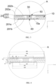
FIG. 1 is a schematic diagram of an overall structure of an electrode plate according to an embodiment of this application, showing a top view; -
FIG. 2 is a sectional side view of an overall structure of an electrode plate according to an embodiment of this application; -
FIG. 3 is an enlarged schematic diagram of a structure at A inFIG. 2 ; -
FIG. 4 is another annotated schematic diagram of a structure at A inFIG. 2 ; -
FIG. 5 is another annotated schematic diagram of an overall structure of an electrode plate according to an embodiment of this application; -
FIG. 6 is a schematic diagram of an overall structure of another embodiment of an electrode plate according to this application; -
FIG. 7 is a schematic diagram of an overall structure of still another embodiment of an electrode plate according to this application; -
FIG. 8 is a schematic diagram of a state of an electrode plate according to an embodiment of this application; -
FIG. 9 is a schematic diagram of another state of an electrode plate according to an embodiment shown inFIG. 8 ; -
FIG. 10 is an exploded schematic diagram of an overall structure of an electrochemical apparatus according to an embodiment of this application; -
FIG. 11 is a sectional side view of some components of an electrode assembly of an electrochemical apparatus according to an embodiment of this application; and -
FIG. 12 is an enlarged schematic diagram of a structure at B inFIG. 11 . - For ease of understanding this application, the following further describes this application in detail with reference to the accompanying drawings and specific embodiments. It should be noted that when an element is "fixed to" another element, the element may be directly on the another element, or there may be one or more elements between the elements. When an element is "connected to" another element, the element may be directly connected to the another element, or there may be one or more elements between the elements. Terms such as "vertical", "horizontal", "left", "right", and similar expressions used in this specification are for illustration only.
- Unless otherwise defined, all technical and scientific terms used herein shall have the same meanings as commonly understood by those skilled in the art to which this application belongs. The terms used in the specification of this application are merely intended to describe specific embodiments but not to constitute any limitations on this application. The term "and/or" used in this specification includes any and all combinations of one or more relevant listed items.
- In addition, technical features involved in different embodiments of this application that are described below may be combined as long as they do not conflict with each other.
- As an important component of an
electrode assembly 102, anelectrode plate 1000 typically needs to be stacked or wound. In order to facilitate stacking or winding, theelectrode plate 1000 may be configured in a strip shape, and theelectrode plate 1000 has a length direction, a width direction, and a thickness direction. During winding, theelectrode plate 1000 is typically wound along a length direction of theelectrode plate 1000. As shown inFIG. 1 andFIG. 2 , the length direction of theelectrode plate 1000 is direction X inFIG. 1 andFIG. 2 , the width direction is direction Y inFIG. 1 , and the thickness direction is direction Z inFIG. 2 . The direction X, direction Y, and direction Z are perpendicular to each other. - Referring to
FIG. 1 andFIG. 2 , theelectrode plate 1000 includes acurrent collector 10, anactive substance layer 20, atab 30, a firstinsulation adhesive layer 40, and a secondinsulation adhesive layer 50. Theactive substance layer 20 is disposed on surface of thecurrent collector 10, thetab 30 is connected to thecurrent collector 10, and the firstinsulation adhesive layer 40 and the secondinsulation adhesive layer 50 are both disposed on a side of theactive substance layer 20 facing away from thecurrent collector 10. - As for the
current collector 10 and thetab 30, as shown inFIG. 1 , thecurrent collector 10 is a conductive substrate of theelectrode plate 1000, and one end of thetab 30 is connected to thecurrent collector 10, and another end of thetab 30 extends in the Y direction. Theelectrode plate 1000 typically includes a positive electrode plate and a negative electrode plate. Depending on a type ofelectrode plate 1000, different materials can be chosen as thecurrent collector 10 of theelectrode plate 1000. For example, aluminum foil can be used as thecurrent collector 10 for a positive electrode plate, and copper foil can be chosen as thecurrent collector 10 for a negative electrode plate. A material of thetab 30 can vary depending on a type of electrode plate, and thetab 30 may be made of metal such as copper, nickel, or aluminum. In some embodiments, thecurrent collector 10 includes a first surface and a second surface disposed opposite each other, and the first surface and the second surface may be coated with theactive substance layer 20. - As for the
active substance layer 20, as shown inFIG. 2 andFIG. 3 , theactive substance layer 20 may be disposed on at least one surface of thecurrent collector 10. Since thecurrent collector 10 is the conductive substrate of theelectrode plate 1000 and typically is in a strip shape, theactive substance layer 20 is typically applied on the first surface or the second surface of theelectrode plate 1000, or theactive substance layer 20 is applied on both the first surface and the second surface of theelectrode plate 1000. In some embodiments, theactive substance layer 20 includes a firstactive substance layer 201 and a secondactive substance layer 202, where the firstactive substance layer 201 is disposed on the first surface, and the secondactive substance layer 202 is disposed on the second surface. - The
active substance layer 20 typically includes active materials, conductive agents, dispersing agents, additives, binders, and the like. Depending on the type ofelectrode plates 1000, different active materials can be chosen for theactive substance layer 20. For the positive electrode plate, common positive active materials can be chosen for theactive substance layer 20, such as lithium cobalt oxide, lithium-rich manganese base, lithium iron phosphate, lithium manganese iron phosphate, nickel cobalt manganese ternary, lithium manganate, polyanionic compound, and Prussian blue, and one or more of the foregoing positive active materials can be chosen for theactive substance layer 20 of the positive electrode plate. For the negative electrode plate, common negative active materials can be chosen for theactive substance layer 20, such as hard carbon, soft carbon, graphite, lithium metal, silicon carbon silicon oxide, and lithium titanate, and one or more of the foregoing negative active materials can be chosen for theactive substance layer 20 of the negative electrode plate. - In some embodiments, the
active substance layer 20 is provided with afirst groove 201a and asecond groove 201b running through the bottom of thefirst groove 201a to thecurrent collector 10. Thecurrent collector 10 is partially exposed within thesecond groove 201b, and the firstinsulation adhesive layer 40 is disposed on a side of thefirst groove 201a facing away from thecurrent collector 10. Projections of the firstinsulation adhesive layer 40 and thetab 30 along the thickness direction of the current collector 10 (that is, along direction Z) are located within thefirst groove 201a of theactive substance layer 20. Thefirst groove 201a is used to accommodate the firstinsulation adhesive layer 40, so that the direct adhesion of the firstinsulation adhesive layer 40 to the surface of the electrode plate is reduced, thereby reducing its influence on the thickness of the electrode plate. Optionally, thefirst groove 201a and thesecond groove 201b are located on the firstactive substance layer 201. - In some embodiments, referring to
FIG. 4 , depth of thefirst groove 201a along a first direction (that is, direction Z) is T1, thickness of the firstinsulation adhesive layer 40 along the first direction is T2, thickness of the firstactive substance layer 201 along the first direction is T3, and T2 ≤ T1 < T3. With such arrangement, the firstinsulation adhesive layer 40 does not extend beyond an edge of the opening of thefirst groove 201a along direction Z, reducing the protrusion of the firstinsulation adhesive layer 40 from the surface of the electrode plate, so as to reduce its influence on the thickness of the electrode plate. The first direction is a direction perpendicular to the bottom of thefirst groove 201a. It should be noted that the specific values of T1, T2, and T3 in this embodiment are not specifically limited, and the specific values of T1, T2, and T3 can be set based on an actual need, as long as the relationship between T1, T2, and T3 satisfies the foregoing conditions. - In some embodiments, width of the
second groove 201b along a second direction (that is, along direction X) is W1, width of the firstinsulation adhesive layer 40 along the second direction is W2, width of thefirst groove 201a along the second direction is W3, and W1 ≤ W2 ≤ W3. With such arrangement, during winding or stacking of the electrode plates, the firstinsulation adhesive layer 40 is located within thefirst groove 201a along direction X, reducing the protrusion of the firstinsulation adhesive layer 40 from the surface of the electrode plate, thereby reducing its influence on the thickness of the electrode plate. It should be noted that the specific values of W1, W2, and W3 in this embodiment are not specifically limited, and the specific values of W1, W2, and W3 can be set based on an actual need, as long as the relationship between W1, W2, and W3 satisfies the foregoing conditions. - In some embodiments, referring to
FIG. 5 and FIG. 6 , when viewed along the thickness direction (that is, direction Z) of thecurrent collector 10, the bottom of thefirst groove 201a is separated by thesecond groove 201b to form a discontinuous first zone 201aa and second zone 201ab, where the first zone and the second zone are arranged opposite each other. One end of the firstinsulation adhesive layer 40 is located in the first zone, and another end is located in the second zone. Alternatively, when viewed along the thickness direction of thecurrent collector 10, the bottom of thefirst groove 201a is separated by thesecond groove 201b to form a third zone 201ac, where the third zone is U-shaped. In addition, as for a shape of thefirst groove 201a and thesecond groove 201b, a concave shape of thefirst groove 201a and thesecond groove 201b in some embodiments of this application includes but is not limited to rectangular, square, cylindrical, and conical shapes. - In some embodiments, as shown in
FIG. 3 , the secondactive substance layer 202 is provided with athird groove 202a and afourth groove 202b running through the bottom of thethird groove 202a to thecurrent collector 10. Thecurrent collector 10 is partially exposed within thefourth groove 202b, and projections of thefourth groove 202b and thesecond groove 201b along the first direction overlap. The secondinsulation adhesive layer 50 is disposed on a side of thethird groove 202a facing away from thecurrent collector 10. Thethird groove 202a is used to accommodate the secondinsulation adhesive layer 50, so that the direct adhesion of the secondinsulation adhesive layer 50 to another surface of the electrode plate is reduced, so as to reduce its influence on the thickness of the electrode plate. - In some embodiments, the
current collector 10 bends towards thefourth groove 202b to form a bendingportion 10a. The bendingportion 10a can be used for connecting thetab 30, and the bendingportion 10a can reduce the influence of thetab 30 on the thickness direction of the electrode plate in direction Z. - In some embodiments, referring to
FIG. 4 , depth of thethird groove 202a along the first direction is T4, thickness of the secondinsulation adhesive layer 50 along the first direction is T5, thickness of the secondactive substance layer 202 along the first direction is T6, where T5 ≤ T4 < T6. With such arrangement, the secondinsulation adhesive layer 50 does not extend beyond an edge of the opening of thethird groove 202a along direction Z, reducing the protrusion of the secondinsulation adhesive layer 50 from the surface of the electrode plate, thereby reducing its influence on the thickness of the electrode plate. It should be noted that the specific values of T4, T5, and T6 in this embodiment are not specifically limited, and the specific values of T4, T5, and T6 can be set based on an actual need, as long as the relationship between T4, T5, and T6 satisfies the foregoing conditions. - In some embodiments, width of the
fourth groove 202b along a second direction (that is, along direction X) is W4, width of the secondinsulation adhesive layer 50 along the second direction is W5, width of thethird groove 202a along the second direction is W6, and W4 ≤ W5 ≤ W6. With such arrangement, during winding or stacking of the electrode plate, the secondinsulation adhesive layer 50 is located within thethird groove 202a along direction X, reducing the protrusion of the secondinsulation adhesive layer 50 from the surface of the electrode plate, thereby reducing its influence on the thickness of the electrode plate. It should be noted that the specific values of W4, W5, and W6 in this embodiment are not specifically limited, and the specific values of W4, W5, and W6 can be set based on an actual need, as long as the relationship between W4, W5, and W6 satisfies the foregoing conditions. It can be understood that the quantities of thefirst grooves 201a and thethird grooves 202a on the electrode plate are not specifically limited in some embodiments of this application and can be set based on the quantity oftabs 30 on the electrode plate. For example, as shown inFIG. 7 , when the quantity oftabs 30 is 2, the quantity offirst grooves 201a can be set to 2 accordingly. - In addition, the specific formation process of the
first groove 201a and thethird groove 202a is not specifically limited in some embodiments of this application. The formation of thefirst groove 201a is used as an example, as shown inFIG. 8 andFIG. 9 . The firstinsulation adhesive layer 40 is applied on the firstactive substance layer 201, and the secondactive substance layer 202 is provided with anaccommodating groove 202c. Subsequently, the electrode plate is subjected to processes such as pressing. After the processes such as pressing, a part of thecurrent collector 10 and the firstactive substance layer 201 that overlap with theaccommodating groove 202c in projection in direction Z are accommodated within theaccommodating groove 202c, and the firstinsulation adhesive layer 40 moves toward a direction of theaccommodating groove 202c, forming a recess on the firstactive substance layer 201 to create thefirst groove 201a. The firstinsulation adhesive layer 40 is located within thefirst groove 201a. For the formation process of thethird groove 202a, reference may be made to the formation process of thefirst groove 201a. It should be noted that in order for the firstinsulation adhesive layer 40 to move as a whole towards theaccommodating groove 202c, the width of theaccommodating groove 202c along direction X needs to be greater than or equal to the width of the firstinsulation adhesive layer 40 along direction X, and a projection of the first insulation adhesive layer in direction Z is located within theaccommodating groove 202c. - For the first
insulation adhesive layer 40 and the secondinsulation adhesive layer 50, as shown inFIG. 3 , the firstinsulation adhesive layer 40 is disposed on a side of thefirst groove 201a facing away from thecurrent collector 10, and the secondinsulation adhesive layer 50 is disposed on a side of thethird groove 202a facing away from thecurrent collector 10. The firstinsulation adhesive layer 40 is partially adhered to thetab 30, and the secondinsulation adhesive layer 50 is partially adhered to thecurrent collector 10. Projections of the secondinsulation adhesive layer 50 and the firstinsulation adhesive layer 40 at least partially overlap along the thickness direction of thecurrent collector 10, and the secondinsulation adhesive layer 50 and the firstinsulation adhesive layer 40 can prevent welding burrs on thetab 30 from puncturing the separator of the battery cell. Optionally, a material for producing the firstinsulation adhesive layer 40 and the secondinsulation adhesive layer 50 include at least one of polypropylene, polycarbonate, polyester resin, or polyamide. - In some embodiments of this application, a
current collector 10, anactive substance layer 20, atab 30, and a firstinsulation adhesive layer 40 are provided. Theactive substance layer 20 is disposed on the surface of thecurrent collector 10 and is provided with afirst groove 201a and asecond groove 201b running through the bottom of thefirst groove 201a to thecurrent collector 10. Thecurrent collector 10 is partially exposed within thesecond groove 201b. Thetab 30 is accommodated in thefirst groove 201a and thesecond groove 201b, where thetab 30 is connected to thecurrent collector 10. In addition, the firstinsulation adhesive layer 40 is disposed on a side of thefirst groove 201a facing away from thecurrent collector 10. The projections of the firstinsulation adhesive layer 40 and thetab 30 along the thickness direction of thecurrent collector 10 are located within thefirst groove 201a of theactive substance layer 20. With such arrangement, the firstinsulation adhesive layer 40 is adhered to thetab 30, which can prevent welding burrs on thetab 30 from puncturing the separator of the battery cell. In addition, the firstinsulation adhesive layer 40 is disposed within thefirst groove 201a. Thefirst groove 201a is used to accommodate the firstinsulation adhesive layer 40, so that the direct adhesion of the firstinsulation adhesive layer 40 to the surface of the electrode plate is reduced, so as to reduce its influence on the overall thickness of the electrode plate. Further, this reduces the influence of the firstinsulation adhesive layer 40 on the thickness of the battery cell formed by winding or stacking the positive and negative electrode plates, improves the energy density of the battery cell, and enhances the thickness consistency of the battery cell, as well as the fast charging and cycling performance of the battery cell. - In addition, in some embodiments, referring to
FIG. 3 , there is a non-overlapping portion between projections of thesecond groove 201b and thefourth groove 202b in the first direction. With such arrangement, during processes such as pressing on the electrode plate, the non-overlapping portion between thesecond groove 201b and thefourth groove 202b in the first direction provides some displacement space for theactive substance layer 20, reducing the influence of theactive substance layer 20 on the thickness of the battery cell. - This application further provides some embodiments of an
electrochemical apparatus 100. As shown inFIG. 10 , theelectrochemical apparatus 100 includes ahousing 101 and anelectrode assembly 102 located inside thehousing 101. Theelectrode assembly 102 includes a separator 1021 and a first electrode plate 1022 and a second electrode plate 1023 disposed on two sides of the separator 1021 and having opposite polarities. The first electrode plate 1022 is the electrode plate described in the foregoing embodiments. Theelectrode assembly 102 can be formed by winding or stacking the separator 1021 with the first electrode plate 1022 and the second electrode plate 1023. In addition, it should be noted that polarities of the first electrode plate 1022 and the second electrode plate 1023 are not specifically limited. The first electrode plate 1022 or the second electrode plate 1023 can be a positive electrode plate, and the first electrode plate 1022 or the second electrode plate 1023 can be a negative electrode plate, as long as the first electrode plate 1022 and the second electrode plate 1023 have opposite polarities. - In some embodiments, referring to
FIG. 11 andFIG. 12 , the second electrode plate 1023 is provided with a thirdinsulation adhesive layer 1023a, where the thirdinsulation adhesive layer 1023a is disposed on a side of the active substance layer of the second electrode plate 1023 facing away from thecurrent collector 10. The first electrode plate 1022 has two extendedfirst step portions 2011 within thefirst groove 201a, where the twofirst step portions 2011 are spaced apart. The firstinsulation adhesive layer 40 is located between the twofirst step portions 2011, and thefirst step portions 2011 are each provided with a first step surface (not shown). In order to reduce the influence of the thirdinsulation adhesive layer 1023a on the thickness of the battery cell, during the winding or stacking of the first electrode plate 1022 and the second electrode plate 1023, a side of the thirdinsulation adhesive layer 1023a facing away from the active substance layer abuts against the separator 1021 until the separator 1021 abuts against the first step surface, and the thirdinsulation adhesive layer 1023a is at least partially located within thefirst groove 201a, thereby reducing the influence of the thirdinsulation adhesive layer 1023a on the thickness of the battery cell. - In some embodiments, thickness of the
first step portions 2011 in the first direction is T7, thickness of the firstinsulation adhesive layer 40 in the first direction is T2, and T2 ≤ T7. With such arrangement, the thickness of the firstinsulation adhesive layer 40 in the first direction does not extend beyond the thickness of thefirst step portions 2011, so that during the winding or stacking of the first electrode plate 1022 and the second electrode plate 1023, direct contact between the firstinsulation adhesive layer 40 and the thirdinsulation adhesive layer 1023a is reduced, reducing the risk of the firstinsulation adhesive layer 40 pushing the thirdinsulation adhesive layer 1023a out of thefirst groove 201a, and further reducing the influence of the thirdinsulation adhesive layer 1023a on the thickness of the battery cell. - In some embodiments, a distance from the first step surface to the opening of the
first groove 201a is T8, thickness of the thirdinsulation adhesive layer 1023a in the first direction is T9, and T9 ≤ T8. With such arrangement, during the winding or stacking of the first electrode plate 1022 and the second electrode plate 1023, the thirdinsulation adhesive layer 1023a is accommodated within thefirst groove 201a, reducing the risk of the thirdinsulation adhesive layer 1023a protruding from the surface of the first electrode plate 1022, reducing the influence of the thirdinsulation adhesive layer 1023a on the thickness of the battery cell, improving the energy density of the battery cell, and enhancing the thickness consistency of the battery cell. - In some embodiments, a spacing between the two
first step portions 2011 is W7, the width of the firstinsulation adhesive layer 40 in a second direction is W2, and W2 ≤ W7. With such arrangement, the firstinsulation adhesive layer 40 can be accommodated between the twofirst step portions 2011. - In some embodiments, the second electrode plate 1023 is provided with a fourth
insulation adhesive layer 1023b, where the fourthinsulation adhesive layer 1023b is disposed on a side of the active substance layer of the second electrode plate 1023 facing away from thecurrent collector 10. The first electrode plate 1022 has two extendedsecond step portions 2021 within thethird groove 202a, where the twosecond step portions 2021 are spaced apart. The secondinsulation adhesive layer 50 is located between the twosecond step portions 2021, and thesecond step portions 2021 are each provided with a second step surface (not shown). During the winding or stacking of the first electrode plate 1022 and the second electrode plate 1023, a side of the fourthinsulation adhesive layer 1023b facing away from the second electrode plate 1023 abuts against the separator 1021 until the separator 1021 abuts against the second step surface, and the fourthinsulation adhesive layer 1023b is at least partially located within thethird groove 202a, reducing the influence of the fourthinsulation adhesive layer 1023b on the thickness of the battery cell. - In some embodiments, thickness of the
second step portions 2021 in the first direction is T10, thickness of the secondinsulation adhesive layer 50 in the first direction is T5, and T5 ≤ T10. During the winding or stacking of the first electrode plate 1022 and the second electrode plate 1023, direct contact between the secondinsulation adhesive layer 50 and the fourthinsulation adhesive layer 1023b is reduced, reducing the risk of the firstinsulation adhesive layer 40 pushing the thirdinsulation adhesive layer 1023a out of thethird groove 202a, and further reducing the influence of the fourthinsulation adhesive layer 1023b on the thickness of the battery cell. - In some embodiments, a distance from the second step surface to the opening of the
third groove 202a is T11, thickness of the fourthinsulation adhesive layer 1023b in the first direction is T12, and T12 ≤ T11. With such arrangement, during the winding or stacking of the first electrode plate 1022 and the second electrode plate 1023, the fourthinsulation adhesive layer 1023b is accommodated within thethird groove 202a, reducing the risk of the fourthinsulation adhesive layer 1023b protruding from the surface of the first electrode plate 1022, reducing the influence of the fourthinsulation adhesive layer 1023b on the thickness of the battery cell, improving the energy density of the battery cell, and enhancing the thickness consistency of the battery cell. - In some embodiments, a spacing between the two
second step portions 2021 is W8, width of the secondinsulation adhesive layer 50 in a second direction is W5, and W5 ≤ W8. With such arrangement, the secondinsulation adhesive layer 50 can be accommodated between the twosecond step portions 2021. - This application further provides some embodiments of an electronic device, where the electronic device includes the foregoing electrochemical apparatus. For the function and structure of the electrochemical apparatus, reference may be made to the foregoing embodiments and details are not repeated herein.
- The foregoing descriptions are merely some embodiments of this application, but are not intended to limit the patent scope of this application. Any equivalent structural or process transformation made by using the content of the specification and accompanying drawings of this application, or direct or indirect application in other related technical fields shall all fall within the patent protection scope of this application in the same way.
Claims (16)
- An electrode plate comprising a current collector and an active substance layer, wherein the active substance layer is disposed on surface of the current collector, whereinthe current collector comprises a first surface and a second surface arranged opposite each other, the active substance layer is disposed on the first surface, and the active substance layer is provided with a first groove and a second groove, wherein the first surface is partially exposed within the second groove, and along a first direction, a projection of the second groove is located within a projection of the first groove, and the first groove and the second groove are sequentially arranged along the first direction;the current collector is provided with a tab and a first insulation adhesive layer, wherein the tab is accommodated in the first groove and the second groove, and the tab is connected to the current collector; andthe first insulation adhesive layer is disposed within the first groove, and projections of the first insulation adhesive layer and the tab along the first direction are located within the first groove, wherein the first direction is a thickness direction of the electrode plate.
- The electrode plate according to claim 1, wherein
the active substance layer comprises a first active substance layer and a second active substance layer, wherein the first active substance layer is disposed on the first surface, the second active substance layer is disposed on the second surface, and the first groove is located on the first active substance layer. - The electrode plate according to claim 2, wherein
depth of the first groove along the first direction is T1, thickness of the first insulation adhesive layer along the first direction is T2, thickness of the first active substance layer along the first direction is T3, and T2 ≤ T1 < T3. - The electrode plate according to claim 3, wherein
the electrode plate satisfies at least one of the following conditions:width of the second groove along a second direction is W1, width of the first insulation adhesive layer along the second direction is W2, and W1 ≤ W2; orwidth of the first groove along the second direction is W3, W2 ≤ W3, and the second direction is perpendicular to the first direction. - The electrode plate according to claim 3, whereinwhen viewed along the first direction, the bottom of the first groove is separated by the second groove to form a discontinuous first zone and second zone, wherein the first zone and the second zone are disposed opposite each other, one end of the first insulation adhesive layer is located in the first zone, and another end is located in the second zone;
orwhen viewed along the first direction, the bottom of the first groove is separated by the second groove to form a third zone, wherein the third zone is U-shaped. - The electrode plate according to claim 3, whereinthe second active substance layer is provided with a third groove and a fourth groove running through the bottom of the third groove to the current collector, wherein the current collector is partially exposed within the fourth groove, projections of the fourth groove and the second groove along the first direction overlap, and the current collector bends towards the fourth groove to form a bending portion, wherein the tab is connected to the bending portion; andthe electrode plate further comprises a second insulation adhesive layer, wherein the second insulation adhesive layer is disposed on a side within the third groove and facing away from the current collector.
- The electrode plate according to claim 6, wherein
depth of the third groove along the first direction is T4, thickness of the second insulation adhesive layer along the first direction is T5, thickness of the second active substance layer along the first direction is T6, and T5 ≤ T4 < T6. - The electrode plate according to claim 6, wherein
at least one of the following conditions is satisfied:width of the fourth groove along a second direction is W4, width of the second insulation adhesive layer along the second direction is W5, and W4 ≤ W5; orwidth of the third groove along the second direction is W6, W5 ≤ W6, and the second direction is perpendicular to the first direction. - The electrode plate according to any one of claims 6 to 8, wherein there is a non-overlapping portion between the projections of the second groove and the fourth groove along the first direction.
- An electrochemical apparatus comprising a separator and a first electrode plate and a second electrode plate disposed on two sides of the separator and having opposite polarities, wherein the first electrode plate is the electrode plate according to any one of claims 1 to 5.
- An electrochemical apparatus comprising a separator and a first electrode plate and a second electrode plate disposed on two sides of the separator and having opposite polarities, wherein the first electrode plate is the electrode plate according to any one of claims 6 to 8.
- The electrochemical apparatus according to claim 11, whereinthe second electrode plate is provided with a third insulation adhesive layer, wherein the third insulation adhesive layer is disposed on a side of the active substance layer of the second electrode plate facing away from the current collector; andthe first electrode plate has two extended first step portions within the first groove, wherein the two first step portions are spaced apart, the first insulation adhesive layer is located between the two first step portions, and the first step portion is provided with a first step surface, wherein during the winding or stacking of the first electrode plate and the second electrode plate, a side of the third insulation adhesive layer facing away from the active substance layer abuts against the separator until the separator abuts against the first step surface, and the third insulation adhesive layer is at least partially located within the first groove.
- The electrochemical apparatus according to claim 12, wherein
at least one of the following conditions is satisfied:thickness of the first step portion along the first direction is T7, thickness of the first insulation adhesive layer along the first direction is T2, and T2 ≤ T7;a distance from the first step surface to an opening of the first groove is T8, thickness of the third insulation adhesive layer along the first direction is T9, and T9 ≤ T8; ora distance between the two first step portions is W7, width of the first insulation adhesive layer along the second direction is W2, and W2 ≤ W7. - The electrochemical apparatus according to claim 11, whereinthe second electrode plate is provided with a fourth insulation adhesive layer, wherein the fourth insulation adhesive layer is disposed on a side of the active substance layer of the second electrode plate facing away from the current collector; andthe first electrode plate has two extended second step portions within the third groove, wherein the two second step portions are spaced apart, the second insulation adhesive layer is located between the two second step portions, and the second step portion is provided with a second step surface, wherein during the winding or stacking of the first electrode plate and the second electrode plate, a side of the fourth insulation adhesive layer facing away from the active substance layer on the second electrode plate abuts against the separator until the separator abuts against the second step surface, and the fourth insulation adhesive layer is at least partially located within the third groove.
- The electrochemical apparatus according to claim 14, wherein
at least one of the following conditions is satisfied:thickness of the second step portion along the first direction is T10, thickness of the second insulation adhesive layer along the first direction is T5, and T5 ≤ T10;a distance from the second step surface to an opening of the third groove is T11, thickness of the fourth insulation adhesive layer along the first direction is T12, and T12 ≤ T11; ora distance between the two second step portions is W8, width of the second insulation adhesive layer along the second direction is W5, and W5 ≤ W8. - An electronic device, comprising the electrochemical apparatus according to any one of claims 10 to 15.
Applications Claiming Priority (2)
| Application Number | Priority Date | Filing Date | Title |
|---|---|---|---|
| CN202211252684.5A CN115332480B (en) | 2022-10-13 | 2022-10-13 | Pole piece, electrochemical device and electronic equipment |
| PCT/CN2023/121953 WO2024078336A1 (en) | 2022-10-13 | 2023-09-27 | Pole piece, electrochemical device, and electronic device |
Publications (2)
| Publication Number | Publication Date |
|---|---|
| EP4583182A1 true EP4583182A1 (en) | 2025-07-09 |
| EP4583182A4 EP4583182A4 (en) | 2025-12-17 |
Family
ID=83914614
Family Applications (1)
| Application Number | Title | Priority Date | Filing Date |
|---|---|---|---|
| EP23876540.8A Pending EP4583182A4 (en) | 2022-10-13 | 2023-09-27 | POLYPIECE, ELECTROCHEMICAL DEVICE AND ELECTRONIC DEVICE |
Country Status (4)
| Country | Link |
|---|---|
| US (1) | US20250246776A1 (en) |
| EP (1) | EP4583182A4 (en) |
| CN (2) | CN116031364A (en) |
| WO (1) | WO2024078336A1 (en) |
Cited By (1)
| Publication number | Priority date | Publication date | Assignee | Title |
|---|---|---|---|---|
| EP4645578A4 (en) * | 2022-12-31 | 2026-04-29 | Ningde Amperex Technology Ltd | Electrode assembly, battery and electrical device |
Families Citing this family (8)
| Publication number | Priority date | Publication date | Assignee | Title |
|---|---|---|---|---|
| CN116031364A (en) * | 2022-10-13 | 2023-04-28 | 宁德新能源科技有限公司 | A pole piece, electrochemical device and electronic equipment |
| CN116964857A (en) * | 2022-12-26 | 2023-10-27 | 东莞新能源科技有限公司 | Secondary batteries and electronic devices |
| CN117501531A (en) * | 2022-12-30 | 2024-02-02 | 宁德新能源科技有限公司 | Electrochemical devices and electronic devices |
| CN115986191A (en) * | 2022-12-31 | 2023-04-18 | 东莞新能源科技有限公司 | Electrochemical devices and electronic equipment |
| CN117423799B (en) * | 2023-12-14 | 2024-03-19 | 珠海冠宇电池股份有限公司 | A pole piece and battery |
| CN117810558A (en) * | 2023-12-28 | 2024-04-02 | 宁德新能源科技有限公司 | Electrode assembly, electrochemical device and electrical equipment |
| WO2026014340A1 (en) * | 2024-07-12 | 2026-01-15 | パナソニックIpマネジメント株式会社 | Non-aqueous electrolyte secondary cell and method for manufacturing non-aqueous electrolyte secondary cell |
| WO2026040792A1 (en) * | 2024-08-20 | 2026-02-26 | 宁德新能源科技有限公司 | Electrode sheet assembly, method for manufacturing electrode sheet assembly, and electrochemical device |
Family Cites Families (19)
| Publication number | Priority date | Publication date | Assignee | Title |
|---|---|---|---|---|
| CN111525180B (en) * | 2015-06-12 | 2022-02-25 | 宁德时代新能源科技股份有限公司 | Secondary battery cells |
| JP6859059B2 (en) * | 2015-09-30 | 2021-04-14 | 積水化学工業株式会社 | Lithium-ion secondary battery and its manufacturing method |
| CN205828514U (en) * | 2016-07-08 | 2016-12-21 | 宁德新能源科技有限公司 | Secondary battery core |
| US11158851B2 (en) * | 2016-10-31 | 2021-10-26 | Envision Aesc Energy Devices Ltd. | Electrode for electrochemical device, electrochemical device, and method for manufacturing same |
| CN111740066B (en) * | 2019-03-25 | 2023-05-12 | 宁德新能源科技有限公司 | Pole piece and electrode assembly with same |
| JP7528262B2 (en) * | 2020-05-11 | 2024-08-05 | チューハイ コスミクス バッテリー カンパニー,リミテッド | Batteries and electronic devices |
| CN212380440U (en) * | 2020-05-22 | 2021-01-19 | 比亚迪股份有限公司 | Winding cells and batteries |
| CN214254465U (en) * | 2020-12-15 | 2021-09-21 | 惠州锂威新能源科技有限公司 | A kind of pole piece for lithium ion battery and lithium ion battery |
| EP4254538A4 (en) * | 2020-12-30 | 2024-09-11 | Ningde Amperex Technology Limited | ELECTRODE ARRANGEMENT AND ELECTROCHEMICAL DEVICE |
| CN112750978B (en) * | 2020-12-30 | 2022-03-15 | 珠海冠宇电池股份有限公司 | Pole piece and battery |
| CN113381058B (en) * | 2021-06-09 | 2023-10-31 | 珠海冠宇电池股份有限公司 | A lithium-ion battery |
| CN216145643U (en) * | 2021-08-10 | 2022-03-29 | 惠州锂威新能源科技有限公司 | Electrode plate, secondary battery and power utilization device thereof |
| EP4386966A4 (en) * | 2021-09-30 | 2025-06-25 | Ningde Amperex Technology Ltd. | CELL AND ELECTRICAL DEVICE THEREOF |
| CN216354301U (en) * | 2021-12-06 | 2022-04-19 | 珠海冠宇电池股份有限公司 | Pole piece and battery |
| CN217062158U (en) * | 2021-12-14 | 2022-07-26 | 惠州锂威新能源科技有限公司 | Battery pole piece and battery cell |
| CN114464769B (en) * | 2021-12-17 | 2024-08-06 | 宁德新能源科技有限公司 | Electrode assembly, electrochemical device, and electricity using device |
| CN114361734B (en) * | 2022-03-21 | 2022-06-17 | 宁德新能源科技有限公司 | Electricity core subassembly, electrochemistry device and consumer |
| CN114843442B (en) * | 2022-07-04 | 2022-09-09 | 宁德新能源科技有限公司 | Electrochemical devices and electronic equipment |
| CN116031364A (en) * | 2022-10-13 | 2023-04-28 | 宁德新能源科技有限公司 | A pole piece, electrochemical device and electronic equipment |
-
2022
- 2022-10-13 CN CN202310128714.XA patent/CN116031364A/en active Pending
- 2022-10-13 CN CN202211252684.5A patent/CN115332480B/en active Active
-
2023
- 2023-09-27 EP EP23876540.8A patent/EP4583182A4/en active Pending
- 2023-09-27 WO PCT/CN2023/121953 patent/WO2024078336A1/en not_active Ceased
-
2025
- 2025-04-14 US US19/178,151 patent/US20250246776A1/en active Pending
Cited By (1)
| Publication number | Priority date | Publication date | Assignee | Title |
|---|---|---|---|---|
| EP4645578A4 (en) * | 2022-12-31 | 2026-04-29 | Ningde Amperex Technology Ltd | Electrode assembly, battery and electrical device |
Also Published As
| Publication number | Publication date |
|---|---|
| CN115332480B (en) | 2023-03-24 |
| CN116031364A (en) | 2023-04-28 |
| WO2024078336A1 (en) | 2024-04-18 |
| CN115332480A (en) | 2022-11-11 |
| US20250246776A1 (en) | 2025-07-31 |
| EP4583182A4 (en) | 2025-12-17 |
Similar Documents
| Publication | Publication Date | Title |
|---|---|---|
| EP4583182A1 (en) | Pole piece, electrochemical device, and electronic device | |
| US10741820B2 (en) | Rechargeable battery | |
| US20160006070A1 (en) | Flexible secondary battery | |
| KR102944814B1 (en) | Secondary battery | |
| EP4395045A1 (en) | Battery core, battery, and electronic device | |
| US20240297421A1 (en) | Electrochemical apparatus and electronic apparatus containing same | |
| CN114975864A (en) | Pole piece, cell structure, lithium battery and electronic equipment | |
| CN116053714A (en) | Electrode assembly, battery and electrical equipment | |
| CN116598601A (en) | Batteries and electrical equipment | |
| US12315960B2 (en) | Current collecting member and manufacturing method thereof, secondary battery and manufacturing method thereof, battery module, and apparatus | |
| US20120321931A1 (en) | Secondary battery | |
| WO2025185402A1 (en) | Battery cell, battery cell preparation method, and electrical device | |
| WO2026001900A1 (en) | Battery cell and electric device | |
| EP4583215A1 (en) | Battery and electronic apparatus | |
| CN116581396A (en) | Batteries and electrical equipment | |
| CN114976512A (en) | Pole piece, electric core structure, lithium battery and electronic equipment | |
| KR102546635B1 (en) | Method of manufacturing pocketing positive electrode body and pocketing positive electrode body | |
| US20260128383A1 (en) | Cell and electric device | |
| KR20160107604A (en) | Secondary battery and the manufacturing method of the same | |
| US20250118864A1 (en) | Electrochemical device and electric device | |
| CN222995471U (en) | Batteries and electronic devices | |
| CN219303736U (en) | Batteries and Terminals | |
| US20240079737A1 (en) | Electrode assembly, electrochemical apparatus, and electric device | |
| WO2025000509A1 (en) | Battery cell and electric device | |
| US20230238664A1 (en) | Electrode assembly and electronic device |
Legal Events
| Date | Code | Title | Description |
|---|---|---|---|
| STAA | Information on the status of an ep patent application or granted ep patent |
Free format text: STATUS: THE INTERNATIONAL PUBLICATION HAS BEEN MADE |
|
| PUAI | Public reference made under article 153(3) epc to a published international application that has entered the european phase |
Free format text: ORIGINAL CODE: 0009012 |
|
| STAA | Information on the status of an ep patent application or granted ep patent |
Free format text: STATUS: REQUEST FOR EXAMINATION WAS MADE |
|
| 17P | Request for examination filed |
Effective date: 20250331 |
|
| AK | Designated contracting states |
Kind code of ref document: A1 Designated state(s): AL AT BE BG CH CY CZ DE DK EE ES FI FR GB GR HR HU IE IS IT LI LT LU LV MC ME MK MT NL NO PL PT RO RS SE SI SK SM TR |
|
| A4 | Supplementary search report drawn up and despatched |
Effective date: 20251113 |
|
| RIC1 | Information provided on ipc code assigned before grant |
Ipc: H01M 4/13 20100101AFI20251107BHEP Ipc: H01M 50/531 20210101ALI20251107BHEP Ipc: H01M 50/59 20210101ALI20251107BHEP Ipc: H01M 50/586 20210101ALI20251107BHEP Ipc: H01M 10/058 20100101ALI20251107BHEP Ipc: H01M 10/0525 20100101ALI20251107BHEP Ipc: H01M 4/66 20060101ALI20251107BHEP |
|
| DAV | Request for validation of the european patent (deleted) | ||
| DAX | Request for extension of the european patent (deleted) |