EP4582955A1 - System and method of checking integrity of an instruction decoder of a processing system - Google Patents
System and method of checking integrity of an instruction decoder of a processing system Download PDFInfo
- Publication number
- EP4582955A1 EP4582955A1 EP24220304.0A EP24220304A EP4582955A1 EP 4582955 A1 EP4582955 A1 EP 4582955A1 EP 24220304 A EP24220304 A EP 24220304A EP 4582955 A1 EP4582955 A1 EP 4582955A1
- Authority
- EP
- European Patent Office
- Prior art keywords
- instruction
- parity
- value
- checker
- bits
- Prior art date
- Legal status (The legal status is an assumption and is not a legal conclusion. Google has not performed a legal analysis and makes no representation as to the accuracy of the status listed.)
- Pending
Links
Images




Classifications
-
- G—PHYSICS
- G06—COMPUTING OR CALCULATING; COUNTING
- G06F—ELECTRIC DIGITAL DATA PROCESSING
- G06F11/00—Error detection; Error correction; Monitoring
- G06F11/07—Responding to the occurrence of a fault, e.g. fault tolerance
- G06F11/08—Error detection or correction by redundancy in data representation, e.g. by using checking codes
- G06F11/10—Adding special bits or symbols to the coded information, e.g. parity check, casting out 9's or 11's
- G06F11/1004—Adding special bits or symbols to the coded information, e.g. parity check, casting out 9's or 11's to protect a block of data words, e.g. CRC or checksum
-
- G—PHYSICS
- G06—COMPUTING OR CALCULATING; COUNTING
- G06F—ELECTRIC DIGITAL DATA PROCESSING
- G06F11/00—Error detection; Error correction; Monitoring
- G06F11/07—Responding to the occurrence of a fault, e.g. fault tolerance
- G06F11/08—Error detection or correction by redundancy in data representation, e.g. by using checking codes
- G06F11/10—Adding special bits or symbols to the coded information, e.g. parity check, casting out 9's or 11's
- G06F11/1008—Adding special bits or symbols to the coded information, e.g. parity check, casting out 9's or 11's in individual solid state devices
- G06F11/1048—Adding special bits or symbols to the coded information, e.g. parity check, casting out 9's or 11's in individual solid state devices using arrangements adapted for a specific error detection or correction feature
-
- G—PHYSICS
- G06—COMPUTING OR CALCULATING; COUNTING
- G06F—ELECTRIC DIGITAL DATA PROCESSING
- G06F9/00—Arrangements for program control, e.g. control units
- G06F9/06—Arrangements for program control, e.g. control units using stored programs, i.e. using an internal store of processing equipment to receive or retain programs
- G06F9/30—Arrangements for executing machine instructions, e.g. instruction decode
- G06F9/30145—Instruction analysis, e.g. decoding, instruction word fields
- G06F9/30156—Special purpose encoding of instructions, e.g. Gray coding
Definitions
- Lockstep configurations for example, have been developed to meet functional safety standards while not complicating software development.
- a pair of processors perform identical operations at about the same time providing redundancy to improve reliability and integrity and to provide a high level of detection coverage in the event of failure.
- An obvious drawback of a lockstep configuration is the cost as this approach requires complete duplication of the processor along with a comparison of every output signal, resulting in die size and power consumption penalties resulting in increased cost.
- Another issue is that random or asynchronous glitches caused by radiation or power or clock abnormalities impacting only one of the processors may be interpreted as a lockstep fault in which operation is halted, triggering complicated and time-consuming test procedures to be performed to identify the faulty device, if any.
- the EX stage 206 executes the instruction in accordance with OPTYPE which may include using any immediate value, accessing register values from source registers using the RS1_ID and RS2_ID identifiers, writing a register value to a destination register using the RD_ID identifier, transferring information to/from memory, etc.
- the register WB stage 208 performs memory load and register write-back functions that are not further described.
- the ID checker 304 extracts one or more of the OPCODE, RS1_ID, RS2_ID, RD_ID, and IMM values from the INST, and provides included values to respective inputs of an ID parity checker 312. It is noted that OPCODE may be extracted from the INST and used along with other extracted information to generate the OPTYPE value in a similar manner previously described. Alternatively, OPTYPE value may be retrieved from the ID stage 204 of the primary processor pipeline 104.
- the ID checker 304 includes a byte to field parity converter 314 that converts the INST bits and the IBP bits into predicted field parity (PPAR) bits based on instruction type indicated by the OPTYPE value as further described herein.
- the OPTYPE value distinguishes between one of six different instruction types, including a register type (R-type), an immediate type (I-type), a store type (S-type), a branch type (B-type), an unsigned immediate type (U-type), and a jump type (J-type).
- the PPAR bits are provided to respective inputs of the ID parity checker 312, which may validate selected instruction fields up to all of the OPCODE, RS1_ID, RS2_ID, RD_ID, and IMM values as further described herein. It is noted that at least one of the PPAR bits is provided for each provided one of the OPCODE, RS1_ID, RS2_ID, RD_ID, and IMM values.
- RS1_PPAR is generally used to validate RS1_ID
- RS2_PPAR is generally used to validate RS2_ID.
- the EX parity checker 316 may check the validity of each received value independently in a similar manner as the ID parity checker 312. In the event an integrity check fails, the EX parity checker 316 asserts one or more second fault detect signals FD2 provided to the fault detector 318. The fault detector 318 asserts the FD signal upon detection of any fault indicated by assertion of any one of the FD1 and FD2 signals.
- a 3-bit functional value FUNCT3 is provided in INST[14:12]
- a 5-bit register ID RS1_ID for source register RS1 is provided in INST[19:15].
- a 5-bit register ID RS2_ID for source register RS2 is provided in INST[24:20].
- a 7-bit functional value FUNCT7 is provided in INST[31:25]
- instruction type I a 12-bit immediate value IMM[11:0] is provided in INST[31:20].
- instruction type S the remaining 7 bits of the immediate value, or IMM[11:5], are provided in INST[31:25].
- the RS1_ID value and its corresponding predicted parity value RS1_PPAR may be provided to a combiner 602, which appends these values as RS1_ID / RS1_PPAR forwarded to the EX checker 306, and the RS2_ID value and its corresponding predicted parity value RS2_PPAR may be provided to a combiner 604, which appends these values as RS2_ID / RS2_PPAR forwarded to the EX checker 306.
- Any additional combiners may be included to combine other extracted values with corresponding predicted parity values in similar manner.
- the combiners 602 and 604 are shown as separate modules, a single combiner may be used to append and forward any of the values in similar manner.
- Selected ones of the extracted values may be provided to a parity calculator 606, which determines calculated (or actual) parity values for the extracted values.
- OPCODE, IMM, RS1_ID, RS2_ID, and RD ID are provided to respective inputs of the parity calculator 606, which calculates and outputs corresponding calculated parity values OPCODE_CPAR, IMM CPAR, RS1 CPAR, RS2_CPAR, and RD_CPAR, respectively. Then each calculated parity is compared with the corresponding predicted parity for verification.
- OPCODE_CPAR and OPCODE_PPAR are provided to respective inputs of a parity comparator 608 to provide a parity error value OPCODE_PERR.
- IMM_CPAR and IMM PPAR are provided to respective inputs of a parity comparator 610 to provide a parity error value IMM_PERR.
- RS1_CPAR and RS1_PPAR may be provided to respective inputs of a parity comparator 612 to provide a parity error value RS1_PERR
- RS2_CPAR and RS2_PPAR may be provided to respective inputs of a parity comparator 614 to provide a parity error value RS2_PERR
- RD_CPAR and RD_PPAR may be provided to respective inputs of a parity comparator 616 to provide a parity error value RD_PERR.
- parity comparators 608, 610, 612, 614, and 616 are shown as separate modules, a single parity comparator may be used for determining the corresponding parity error values.
- FD1 may be a multiple-bit signal in which the parity error values OPCODE_PERR, IMM_PERR, RS1_PERR, RS2_PERR, and RD_PERR may be provided as respective bits of FD1[4:0].
- FD1 may be a single bit that is asserted when any one or more of the PERR values are asserted.
- FIG. 7 is a flowchart diagram illustration operation of the checker pipeline 110 for verifying operation of the ID stage 204 of the primary processor pipeline 104 according to one embodiment.
- instruction correction information received while fetching the instruction such as ECC bits or the like, is converted into instruction byte parity information (e.g., instruction byte parity bits).
- This function may be performed, for example, by the ECC to byte parity converter 310 provided within the IF checker 302 for verifying the received instruction INST.
- Operation advances to block 704 in which the instruction byte parity information and instruction information (e.g., instruction bits) are converted into predicted parity information (e.g., predicted parity value for each instruction field value).
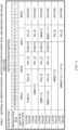
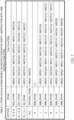
- This function may be performed, for example, by the byte to field parity converter 314 of the ID checker 304 in accordance with the mapping shown by Table 1 in FIG. 4 and logic XOR calculations shown by Table 2 in FIG. 5 for determining the PPAR values for each field value.
- Operation advances to block 706 in which the instruction field values are extracted from the instruction INST based on instruction type.
- the instruction field values may include OPCODE, RS1_ID, RS2_ID, RD_ID, and IMM depending upon the instruction type as shown in FIG. 4 .
- Operation advances to block 708 to calculate parity information for each of the instruction field values, such as performed by the ID parity checker 312 of the ID checker 304 or the EX parity checker 316 of the EX checker 306.
- Each calculated parity value may be considered an actual parity value for the actual bits of the field values received from the ID stage 204.
- any number (including zero) up to all of the parity calculations may be performed within the ID checker 304, such as determining the OPCODE_CPAR, RD_CPAR, and IMM_CPAR values shown in FIG. 6 . Also, any number (including zero) up to all of the parity calculations may be performed within the EX checker 306, which may also perform combined parity verification determinations such as shown and described for the source register identifier values RS1_ID and RS2_ID.
- Operation then advances to block 710 for comparing calculated parity information with predicted parity information for providing parity error information used for fault detection, such as comparing each calculated parity value with a corresponding predicted parity value for each instruction field value for determining a corresponding parity error value.
- parity error information used for fault detection, such as comparing each calculated parity value with a corresponding predicted parity value for each instruction field value for determining a corresponding parity error value.
- any number (including zero) up to all of the parity calculated versus predicted comparisons may be performed by the ID parity checker 312 of the ID checker 304, or any number up to all may be performed by the EX parity checker 316. Operation is then completed for the current instruction, and operation repeats for each instruction fetched from memory.
- the fault detector 318 asserts the FD signal indicating detection of a fault.
- the self-checking processing system 100 may take any suitable remedial or corrective action, not further described herein. Notification of the fault may also be provided.
- the ID checker 304 of the checker pipeline 110 performs validation of the ID stage 204 of the primary processor pipeline 104 without replicating the ID stage 204. Instead, error correction information received during the instruction memory bus transaction to fetch the instructions INST, such as ECC bits or the like, are converted to instruction byte parity information and then to instruction field parity information and used to validate the instruction decoder function by validating each of the values extracted by the instruction decoder of the primary processor pipeline.
- circuitry states such as circuitry low and circuitry high may be reversed depending upon whether the pin or signal is implemented in positive or negative circuitry or the like.
- the circuitry state may be programmable in which the circuitry state may be reversed for a given circuitry function.
Landscapes
- Engineering & Computer Science (AREA)
- Theoretical Computer Science (AREA)
- General Engineering & Computer Science (AREA)
- Physics & Mathematics (AREA)
- General Physics & Mathematics (AREA)
- Software Systems (AREA)
- Quality & Reliability (AREA)
- Computer Security & Cryptography (AREA)
- Detection And Correction Of Errors (AREA)
Abstract
Description
- The present disclosure relates in general to processor data integrity, and more particularly to a system and method of checking the integrity of an instruction decoder of a processing system.
- System reliability and safety are major concerns for many types of electrical and electronics systems, including Systems-on-Chip ("SoCs"). For example, in the automotive industry, the complexity of applications has been ever increasing, resulting in a higher chance of failure of hardware or software. Standards and metrics for functional safety, such as ASIL-D (Automotive Safety Integrity Level D) for vehicle systems, require that the designs of electrical and electronics systems have to be robust enough that failures can be detected so that corrective actions can be taken.
- Lockstep configurations, for example, have been developed to meet functional safety standards while not complicating software development. In a lockstep configuration, a pair of processors perform identical operations at about the same time providing redundancy to improve reliability and integrity and to provide a high level of detection coverage in the event of failure. An obvious drawback of a lockstep configuration is the cost as this approach requires complete duplication of the processor along with a comparison of every output signal, resulting in die size and power consumption penalties resulting in increased cost. Another issue is that random or asynchronous glitches caused by radiation or power or clock abnormalities impacting only one of the processors may be interpreted as a lockstep fault in which operation is halted, triggering complicated and time-consuming test procedures to be performed to identify the faulty device, if any.
- In a processor pipeline implementation, the instruction decoder is typically a combinational logic control function in the execution pipeline. Standard error detecting code approaches like parity codes and/or residue codes cannot be directly used to validate the correct functionality of the instruction decoder. Traditional processor monitoring approaches required duplication of the instruction decoder for purposes of data integrity verification.
- Embodiments of the present disclosure are illustrated by way of example and are not limited by the accompanying figures. Similar references in the figures may indicate similar elements. Elements in the figures are illustrated for simplicity and clarity and have not necessarily been drawn to scale.
-
FIG. 1 is a simplified block diagram of one example of a self-checking processing system implemented according to one embodiment. -
FIG. 2 is a simplified block diagram of the primary processor pipeline ofFIG. 1 implemented according to one embodiment. -
FIG. 3 is a simplified block diagram of a portion of the checker pipeline ofFIG. 1 implemented according to one embodiment. -
FIG. 4 shows a first table TABLE 1 that maps instruction bits, instruction byte parity bits, and instruction fields per instruction type according to one embodiment. -
FIG. 5 shows a second table TABLE 2 that illustrates predicted field parity (PPAR) calculations based on the instruction byte parity (IBP) bits, corresponding instruction bits, and the instruction type (as indicated by an instruction or operation (OPTYPE) value) performed by the byte to field parity converter ofFIG. 3 according to one embodiment. -
FIG. 6 is a simplified block diagram of the instruction decode (ID) parity checker ofFIG. 3 implemented according to one embodiment. -
FIG. 7 is a flowchart diagram illustrating operation of the checker pipeline ofFIG. 1 for verifying operation of the ID stage of the primary processor pipeline according to one embodiment. - Complete replication of the instruction decoder of a primary processor pipeline for purposes of verification and integrity checking is avoided. Instead, error correcting code information received during the instruction memory bus transaction to fetch the instructions is used to check the integrity of the instruction decoder, all part of implementing a fault-tolerant processor core. In a Functional Safety (FuSa) compliant system-on-a-chip (SoC), the memory bus transactions used to fetch the instructions are protected by some additional information such as byte parity bits or error-correcting code bits (ECC, typically a single-error correct/double-error detect (SEC/DED ECC)). This additional information received during the bus transaction to fetch instructions is used to validate the instruction decoder function. The received instruction correction information is converted to instruction byte parity information, which is further converted to predicted field parity information that may be used to check integrity of each of the field values contained within the instruction.
-
FIG. 1 is a simplified block diagram of one example of a self-checking processing system 100 implemented according to one embodiment. The self-checking processing system 100 includes a primary central processing unit (CPU) 102 that performs execution of instructions relating to the primary functionality of theprocessing system 100. Theprimary CPU 102 has aprimary processor pipeline 104 with multiple stages. For example, theprimary processor pipeline 104 may be a four-stage pipelined CPU with four stages. It should be understood that the set of multiple stages repeats in successive cycles during the operation of theprocessing system 100. Theprocessing system 100 also includes abus interface unit 106 and acore monitor 108. Thecore monitor 108 has achecker pipeline 110 that essentially operates in parallel with theprimary processor pipeline 104 and may have the same number of stages as the primary processor pipeline. Thechecker pipeline 110 is not a duplicate of theprimary processor pipeline 104. Instead, thechecker pipeline 110 operates on check function data only, such as byte parity or residue codes or the like, in order to check the integrity of the operations of theprimary processor pipeline 104. - The
core monitor 108 operates during each of the stages of theprimary processor pipeline 104. Aninternal bus 112 enables communication between theprimary CPU 102 and thebus interface unit 106 and between thecore monitor 108 and thebus interface unit 106. A set ofdata registers 113 may be accessed via theinternal bus 112. Internal CPU signals andcontrols 114 may be provided between theprimary CPU 102 and thecore monitor 108. Thebus interface unit 106 enables access to other devices and systems via asystem bus interface 116, such as amemory system 117. Thecore monitor 108 generates and outputs a fault detection (FD)signal 118 when a fault is detected by thecore monitor 108. - The
core monitor 108 is not a complete duplicate of theprimary CPU 102, and thechecker pipeline 110 is not a complete duplicate of theprimary processor pipeline 104, although operation of thecore monitor 108 generally mirrors operation of theprimary processor pipeline 104. Thecore monitor 108 may perform checking functions during each stage of theprimary processor pipeline 104. Thecore monitor 108 implements checking functions that are used to monitor and verify the executions of theprimary CPU 102, and to detect whether there is a fault in the executions performed by theprimary CPU 102. The type of each checking function may be dynamically selected by thecore monitor 108 based on the corresponding type of operation being performed by theprimary CPU 102. One of the checking functions that may be performed by thecore monitor 108 is a residue check for a CPU arithmetic instruction execution. Another checking function that many be performed by thecore monitor 108 is parity checking for data transfers and logical operations. Parity checking may be byte parity checking, such as odd byte parity checking or even byte parity checking. The checking functions may include a hybrid checking approach that includes performing parity checking for data transfers and logical operations, and residue checking for the CPU arithmetic instruction execution logic. It is noted that parity checking generally provides protection against at least one bit error whereas residue checking provides protection of more complex arithmetic operations. - The figures provided herein illustrate functional blocks of CPU systems. It should be understood that a functional block may be implemented using hardware, software, or a combination of hardware and software. Generally, CPU systems of the present technology include at least one processor, and at least one memory device coupled at least indirectly to the at least one processor. CPU systems of the present technology may include multiple processors and multiple memory devices, where each memory device is coupled at least indirectly to at least one of the multiple processors. Each memory device may be any suitable type of memory device, including for example, volatile or non-volatile memory. The memory devices in the CPU system may include at least one memory storage device that stores computer readable instructions that, when implemented by at least one processor, cause the at least one processor to perform functions in accordance with the methods of the present disclosure.
-
FIG. 2 is a simplified block diagram of theprimary processor pipeline 104 implemented according to one embodiment. In one embodiment, theprimary processor pipeline 104 may be implemented as a four stage RISC-V processor pipeline, although alternative processor configurations and architectures are contemplated. Theprimary processor pipeline 104 includes an instruction fetch (IF)stage 202, an instruction decode (ID)stage 204, an execution (EX)stage 206, and a register write-back (WB)stage 208. TheIF stage 202 receives a program counter (PC) address and generally operates to fetch instructions (INST) from memory and to pass fetched instructions to theID stage 204. TheID stage 204 generally operates to extract information and values from the instruction and to pass extracted information to theEX stage 206. For example, theID stage 204 extracts an OPCODE from the instruction along with any other functional information that may be included (e.g., FUNCT3, FUNCT7) to form an instruction or operation type (OPTYPE) value (e.g., including the OPCODE concatenated with functional values), in which OPYTPE includes control signals indicating the operations or functions to be performed or executed. TheID stage 204 also extracts any register identifiers from the instruction that may be included, such as source register identifiers RS1_ID and RS2_ID and a destination register identifier RD_ID. TheID stage 204 may also extract an immediate value IMM, if present. TheEX stage 206 executes the instruction in accordance with OPTYPE which may include using any immediate value, accessing register values from source registers using the RS1_ID and RS2_ID identifiers, writing a register value to a destination register using the RD_ID identifier, transferring information to/from memory, etc. Theregister WB stage 208 performs memory load and register write-back functions that are not further described. -
FIG. 3 is a simplified block diagram of a portion of thechecker pipeline 110 implemented according to one embodiment. Thechecker pipeline 110 includes an IFchecker 302 for checking and verifying operation of theIF stage 202, anID checker 304 for checking and verifying operation of theID stage 204, and anEX checker 306 for checking and verifying operation of theEX stage 206. Although not shown, thechecker pipeline 110 may also include a WB checker for checking and verifying operation of theregister WB stage 208. The instructions INST received by theIF stage 202 are also provided to theIF checker 302, along with error correction information. The error correction information may be in the form of error-correcting code (ECC) bits ECC_I, which may typically be configured as single-error correct/double-error detect (SEC/DED ECC) bits. Alternative error correction information may be used as well. The ECC information is typically used by a memory controller (not shown) of thememory system 117 and by theIF checker 302 to check the integrity of each INST received. TheIF checker 302 may include an ECC to byteparity converter 310 that converts ECC_I into a set of instruction byte parity (IBP) bits, which includes one parity bit for each byte of the instruction INST. The instruction INST and the IBP bits are forwarded to theID checker 304. - The
ID checker 304 extracts one or more of the OPCODE, RS1_ID, RS2_ID, RD_ID, and IMM values from the INST, and provides included values to respective inputs of anID parity checker 312. It is noted that OPCODE may be extracted from the INST and used along with other extracted information to generate the OPTYPE value in a similar manner previously described. Alternatively, OPTYPE value may be retrieved from theID stage 204 of theprimary processor pipeline 104. TheID checker 304 includes a byte to fieldparity converter 314 that converts the INST bits and the IBP bits into predicted field parity (PPAR) bits based on instruction type indicated by the OPTYPE value as further described herein. In one embodiment, the OPTYPE value distinguishes between one of six different instruction types, including a register type (R-type), an immediate type (I-type), a store type (S-type), a branch type (B-type), an unsigned immediate type (U-type), and a jump type (J-type). The PPAR bits are provided to respective inputs of theID parity checker 312, which may validate selected instruction fields up to all of the OPCODE, RS1_ID, RS2_ID, RD_ID, and IMM values as further described herein. It is noted that at least one of the PPAR bits is provided for each provided one of the OPCODE, RS1_ID, RS2_ID, RD_ID, and IMM values. - In one embodiment, the RS1_ID and RS2_ID values, if provided, are not checked by the
ID parity checker 312; instead, theID parity checker 312 appends a PPAR bit RS1_PPAR to the RS1_ID value and appends a PPAR bit RS2_PPAR to the RS2_ID value and forwards the appended values downstream to theEX checker 306. In this embodiment, theID parity checker 312 checks the integrity of any provided PPAR bits of the remaining values OPCODE, RD_ID, and IMM as further described herein. In the event an integrity check fails, theID parity checker 312 asserts one or more first fault detected signals FD1 provided to afault detector 318. - In one alternative embodiment, the
ID parity checker 312 may instead use the PPAR bits to check each of the provided OPCODE, RS1_ID, RS2_ID, RD_ID, and IMM values for determining the FD1 signal. In another alternative embodiment, theID parity checker 312 may instead simply append each PPAR value to a corresponding one of the provided OPCODE, RS1_ID, RS2_ID, RD_ID, and IMM values and forward each of the appended values downstream to theEX checker 306. - In the illustrated embodiment, the
EX checker 306 includes anEX parity checker 316 that checks the validity of values passed from theID checker 304. If the RS1_ID and corresponding parity value RS1_PPAR are received identifying a first source register, then during operation theEX checker 306 may retrieve a corresponding value RS1_VAL from the set of registers along with a corresponding parity value PAR1. If the RS2_ID and corresponding parity value RS2_PPAR are received identifying a second source register, then during operation theEX checker 306 may retrieve a corresponding value RS2_VAL from the set of registers along with a corresponding parity value PAR2. In one embodiment, theEX checker 306 uses the combined information to perform validation of the corresponding values. For example, theEX parity checker 316 may combine the RS1_ID, RS1_PPAR, RS1_VAL, and PAR1 values for checking the validity of the RS1_ID and RS1_VAL values in a single validity check calculation. Similarly, theEX parity checker 316 may combine the RS2_ID, RS2_PPAR, RS2_VAL, and PAR2 values for checking the validity of the RS2_ID and RS2_VAL values in a single validity check calculation. Providing a verification of multiple values in a combined calculation is more efficient and provides better fault coverage, thereby improving overall performance. - Generally, even when the
EX parity checker 316 performs a combined verification calculation, RS1_PPAR is generally used to validate RS1_ID, and RS2_PPAR is generally used to validate RS2_ID. In an alternative embodiment, theEX parity checker 316 may check the validity of each received value independently in a similar manner as theID parity checker 312. In the event an integrity check fails, theEX parity checker 316 asserts one or more second fault detect signals FD2 provided to thefault detector 318. Thefault detector 318 asserts the FD signal upon detection of any fault indicated by assertion of any one of the FD1 and FD2 signals. -
FIG. 4 shows a first table TABLE 1 that maps instruction bits, instruction byte parity bits, and instruction fields per instruction type according to one embodiment. In the illustrated embodiment, each instruction INST includes 32 bits, or INST[31:0]. The instruction byte parity or IBP bits includes a corresponding 4 bits IBP[3:0], including IBP[0] for the least significant 8-bits (INST[7:0]) of the instruction, IBP[1] for the next significant 8-bits (INST[15:8]) of the instruction, IBP[2] for the next significant 8-bits (INST[23: 16]) of the instruction, and IBP[3] for the most significant 8-bits (INST[31:24]) of the instruction. - For each of the instruction types (R, I, S, B, U, J), the OPCODE is contained within the lower 7 bits of the instruction, or INST[6:0]. For the instruction types R, I, U, and J, the RD_ID value is provided in the next 5 bits of the instruction, or INST[11:7]. For the instruction types S and B, the INST[11:7] bits are used to contain various bits of the IMM value, shown as IMM[4:0] for S_type instruction and IMM[4:1,11] for the B_type instruction. For the instruction types R, I, S, and B, a 3-bit functional value FUNCT3 is provided in INST[14:12], and a 5-bit register ID RS1_ID for source register RS1 is provided in INST[19:15]. For the instruction types R, S, and B, a 5-bit register ID RS2_ID for source register RS2 is provided in INST[24:20]. For instruction type R, a 7-bit functional value FUNCT7 is provided in INST[31:25], for instruction type I, a 12-bit immediate value IMM[11:0] is provided in INST[31:20]. For instruction type S, the remaining 7 bits of the immediate value, or IMM[11:5], are provided in INST[31:25]. For instruction type B, the remaining 7 bits of the immediate value, or IMM[12,10:5], are provided in INST[31:25]. For instruction type U, immediate value bits IMM[31:12] are provided in INST[31:12], and for instruction type J, immediate value bits IMM[20,10:1,11,19:12] are provided in INST[31:12]. It is noted that the FUNCT3 value or the FUNCT3 and FUNCT7 values are combined with the corresponding OPCODE of the corresponding instruction to determine the corresponding OPTYPE value.
- The mappings shown in TABLE 1 are applicable to a particular instruction set architecture and corresponding CPU and may vary between different embodiments. Nonetheless, in each case, overlapping IBP and instruction bits may be logically combined to convert the IBP parity bits into corresponding instruction field parity bits for each of the values contained therein as further described herein.
-
FIG. 5 shows a second table TABLE 2 that illustrates the PPAR calculations based on the IBP bits, corresponding instruction bits, and the instruction type (as indicated by OPTYPE) performed by the byte to fieldparity converter 314 according to one embodiment. An OPTYPE value of "ALL" means that the calculation applies to any of the instruction types R, I, S, B, U, and J. A caret symbol "^" between bit values denotes the Boolean logic exclusive-OR (XOR) operation. In general, for each field value, at least one overlapping instruction byte parity bit is selected and combined by XORing with instruction bits exclusive of the selected overlapping instruction byte parity bit(s) while also inclusive of the field bits and also inclusive of the exclusive of the selected overlapping instruction byte parity bit(s) while also exclusive of the bits of the field value. - As shown, for example, the PPAR value RS2_PPAR for the second source register identifier RS2_ID for the instruction types R, S, and B, is determined by the XOR combination of the indicated bits, or IBP[2] ^ INST[24] ^ INST[19] ^ INST[18] ^ INST[17] ^ INST[16]. Similarly, the PPAR value RS1_PPAR for the first source register identifier RS1_ID for the instruction types R, I, S, and B, is determined by the XOR combination of the indicated bits, or IBP[2] ^ INST[23] ^ INST[22] ^ INST[21] ^ INST[20] ^ INST[15]. Likewise, the PPAR value RD_PPAR for the destination register identifier RD_ID for the instruction types R, I, U, and J, is determined by the XOR combination of the indicated bits, or IBP[1] ^ INST[15] ^ INST[14] ^ INST[13] ^ INST[12] ^ INST[7]. The PPAR value OPCODE_PPAR for the OPCODE value is IBP[0] ^ INST[7] for all of the instructions. The PPAR value IMM_PPAR for the immediate value is shown for each of the instruction types I, S, B, U, and J. Since the R-type instruction does not include an immediate value, IMM_PPAR = 0 for the R-type instruction.
- As previously described, the PPAR values are calculated by the byte to field
parity converter 314 using the IBP and INST bits based on the instruction type as indicated by OPTYPE and provided to theID parity checker 312. TheID parity checker 312 determines the validity of a selected number up to all of the field values of theID stage 204 for determining the FD1 signal. -
FIG. 6 is a simplified block diagram of theID parity checker 312 implemented according to one embodiment. As previously shown inFIG. 3 , theID parity checker 312 receives the OPCODE, RS1_ID, RS2_ID, RD_ID, and IMM values extracted from INST. Selected ones of the extracted values (which may include none up to all of the values) may be combined with corresponding PPAR values and passed on downstream to theEX checker 306, which includes theEX parity checker 316 that performs verification. As shown, for example, the RS1_ID value and its corresponding predicted parity value RS1_PPAR may be provided to acombiner 602, which appends these values as RS1_ID / RS1_PPAR forwarded to theEX checker 306, and the RS2_ID value and its corresponding predicted parity value RS2_PPAR may be provided to acombiner 604, which appends these values as RS2_ID / RS2_PPAR forwarded to theEX checker 306. Any additional combiners may be included to combine other extracted values with corresponding predicted parity values in similar manner. Although thecombiners - Selected ones of the extracted values (including all or any remaining ones, if any) may be provided to a
parity calculator 606, which determines calculated (or actual) parity values for the extracted values. As shown, OPCODE, IMM, RS1_ID, RS2_ID, and RD ID are provided to respective inputs of theparity calculator 606, which calculates and outputs corresponding calculated parity values OPCODE_CPAR, IMM CPAR, RS1 CPAR, RS2_CPAR, and RD_CPAR, respectively. Then each calculated parity is compared with the corresponding predicted parity for verification. As shown, OPCODE_CPAR and OPCODE_PPAR are provided to respective inputs of aparity comparator 608 to provide a parity error value OPCODE_PERR. IMM_CPAR and IMM PPAR are provided to respective inputs of aparity comparator 610 to provide a parity error value IMM_PERR. Similarly, RS1_CPAR and RS1_PPAR may be provided to respective inputs of aparity comparator 612 to provide a parity error value RS1_PERR, RS2_CPAR and RS2_PPAR may be provided to respective inputs of aparity comparator 614 to provide a parity error value RS2_PERR, and RD_CPAR and RD_PPAR may be provided to respective inputs of aparity comparator 616 to provide a parity error value RD_PERR. - Although the
parity comparators -
FIG. 7 is a flowchart diagram illustration operation of thechecker pipeline 110 for verifying operation of theID stage 204 of theprimary processor pipeline 104 according to one embodiment. At afirst block 702, instruction correction information received while fetching the instruction, such as ECC bits or the like, is converted into instruction byte parity information (e.g., instruction byte parity bits). This function may be performed, for example, by the ECC to byteparity converter 310 provided within theIF checker 302 for verifying the received instruction INST. Operation advances to block 704 in which the instruction byte parity information and instruction information (e.g., instruction bits) are converted into predicted parity information (e.g., predicted parity value for each instruction field value). This function may be performed, for example, by the byte to fieldparity converter 314 of theID checker 304 in accordance with the mapping shown by Table 1 inFIG. 4 and logic XOR calculations shown by Table 2 inFIG. 5 for determining the PPAR values for each field value. - Operation advances to block 706 in which the instruction field values are extracted from the instruction INST based on instruction type. The instruction field values may include OPCODE, RS1_ID, RS2_ID, RD_ID, and IMM depending upon the instruction type as shown in
FIG. 4 . Operation advances to block 708 to calculate parity information for each of the instruction field values, such as performed by theID parity checker 312 of theID checker 304 or theEX parity checker 316 of theEX checker 306. Each calculated parity value may be considered an actual parity value for the actual bits of the field values received from theID stage 204. As previously described, any number (including zero) up to all of the parity calculations may be performed within theID checker 304, such as determining the OPCODE_CPAR, RD_CPAR, and IMM_CPAR values shown inFIG. 6 . Also, any number (including zero) up to all of the parity calculations may be performed within theEX checker 306, which may also perform combined parity verification determinations such as shown and described for the source register identifier values RS1_ID and RS2_ID. - Operation then advances to block 710 for comparing calculated parity information with predicted parity information for providing parity error information used for fault detection, such as comparing each calculated parity value with a corresponding predicted parity value for each instruction field value for determining a corresponding parity error value. Again, any number (including zero) up to all of the parity calculated versus predicted comparisons may be performed by the
ID parity checker 312 of theID checker 304, or any number up to all may be performed by theEX parity checker 316. Operation is then completed for the current instruction, and operation repeats for each instruction fetched from memory. - In the event that any one of the FD1 or FD2 signals are asserted during operation of the self-checking
processing system 100, thefault detector 318 asserts the FD signal indicating detection of a fault. Upon assertion of the FD signal, the self-checkingprocessing system 100 may take any suitable remedial or corrective action, not further described herein. Notification of the fault may also be provided. - It is appreciated that the
ID checker 304 of thechecker pipeline 110 performs validation of theID stage 204 of theprimary processor pipeline 104 without replicating theID stage 204. Instead, error correction information received during the instruction memory bus transaction to fetch the instructions INST, such as ECC bits or the like, are converted to instruction byte parity information and then to instruction field parity information and used to validate the instruction decoder function by validating each of the values extracted by the instruction decoder of the primary processor pipeline. - One or more embodiments of the present disclosure may include features recited in the following numbered clauses:
- 1. A checker pipeline for checking integrity of an instruction decode stage of a primary processor pipeline of a processing system, the primary processor pipeline including an instruction fetch stage configured to receive an instruction comprising a plurality of fields and the instruction decoder stage configured to decode the instruction into a plurality of instruction field values, the checker pipeline comprising: an instruction fetch checker configured to receive and convert instruction correction information provided with the instruction into instruction byte parity information; and an instruction decoder checker comprising a parity converter configured to convert the instruction byte parity information and instruction field information into predicted field parity information that is used to check integrity of the plurality of instruction field values of the instruction decoder stage.
- 2. The checker pipeline of
claim 1, wherein the instruction correction information comprises error correction code bits, and wherein the instruction fetch checker comprises an error correction code to byte parity converter configured to convert the error correction code bits into a plurality of instruction byte parity bits. - 3. The checker pipeline of
claim 1, wherein the parity converter is configured to parse the instruction into a plurality of fields based on instruction type, and for each of the plurality of fields, to combine at least one of a plurality of instruction byte parity bits with corresponding instruction bits using a Boolean logic exclusive-OR operation. - 4. The checker pipeline of
claim 1, wherein the parity converter is configured to parse the instruction into a plurality of fields based on instruction type, and for at least one of the plurality of fields, to combine at least one of a plurality of instruction byte parity bits with instruction bits that are exclusive of the at least one of the plurality of fields while also inclusive of the instruction bits associated with the at least one of a plurality of instruction byte parity bits and that are inclusive of the at least one of the plurality of fields while also exclusive of the instruction bits associated with the at least one of a plurality of instruction byte parity bits using a Boolean logic exclusive-OR operation. - 5. The checker pipeline of
claim 1, wherein the instruction decoder checker further comprises: a parity calculator configured to determine a calculated parity value for each of selected ones of the plurality of instruction field values; and a parity comparator configured to compare a predicted field parity value with a calculated parity value for each of the selected ones of the plurality of instruction field values for providing corresponding parity error values. - 6. The checker pipeline of
claim 5, wherein: the plurality of instruction field values comprises an opcode and at least one register identifier; wherein the parity calculator is configured to determine a calculated opcode parity value using the opcode and to determine a calculated register identifier parity value for each of the at least one register identifier; and wherein the parity comparator is configured to compare a predicted opcode parity value with the calculated opcode parity value and is configured to compare a predicted register identifier parity value with a calculated register identifier value for each of the at least one register identifier. - 7. The checker pipeline of
claim 5, wherein: the plurality of instruction field values comprises an immediate value; wherein the parity calculator is configured to determine a calculated immediate parity value using the immediate value; and wherein the parity comparator is configured to compare a predicted immediate parity value with the calculated immediate parity value. - 8. The checker pipeline of
claim 1, wherein the checker pipeline further comprises an execution checker, further comprising: the predicted field parity information comprising a corresponding one of a plurality of predicted field parity values for each of the plurality of instruction field values; wherein the instruction decoder checker comprises a combiner configured to combine and forward at least one predicted field parity value with a corresponding one of the plurality of instruction fields to the execution checker; and wherein the execution checker comprises a comparator checker configured to determine a calculated parity value for each received instruction field value and to compare each calculated parity value with a corresponding predicted field parity value for providing a corresponding parity error value. - 9. The checker pipeline of
claim 1, wherein the checker pipeline further comprises an execution checker, further comprising: the predicted parity information comprising a predicted register identifier parity value for a register identifier value that is provided within the plurality of instruction field values; wherein the instruction decoder checker comprises a combiner configured to combine and forward a predicted register identifier parity value with the register identifier value; and wherein the execution checker is configured to retrieve a register value and corresponding register parity value using the register identifier value, and comprises a parity checker configured to collectively verify the register value and the register identifier value using the predicted register identifier parity value and the register parity value. - 10. A method of checking integrity of an instruction decode stage of a primary processor pipeline of a processing system, the primary processor pipeline including an instruction fetch stage configured to receive an instruction comprising a plurality of fields and the instruction decoder stage configured to decode the instruction into a plurality of instruction field values, the method comprising: receiving and converting instruction correction information provided with the instruction into instruction byte parity information; and converting the instruction byte parity information and instruction field information into predicted field parity information that is used to check integrity of a plurality of instruction field values of the instruction decoder stage.
- 11. The method of
claim 10, wherein the converting instruction correction information comprises converting error correction code bits into a plurality of instruction byte parity bits. - 12. The method of
claim 10, wherein the converting the instruction byte parity information and instruction field information comprises parsing the instruction into a plurality of fields based on instruction type, and for each of the plurality of fields, combining at least one of a plurality of instruction byte parity bits with corresponding instruction bits using a Boolean logic exclusive-OR operation. - 13. The method of
claim 10, wherein the converting the instruction byte parity information and instruction field information comprises parsing the instruction into a plurality of fields based on instruction type, and for at least one of the plurality of fields, combining at least one of a plurality of instruction byte parity bits with instruction bits that are exclusive of the at least one of the plurality of fields while also inclusive of the instruction bits associated with the at least one of a plurality of instruction byte parity bits and that are inclusive of the at least one of the plurality of fields while also exclusive of the instruction bits associated with the at least one of a plurality of instruction byte parity bits using a Boolean logic exclusive-OR operation. - 14. The method of
claim 10, further comprising: determining a calculated parity value for each of selected ones of the plurality of instruction field values; and comparing a predicted field parity value with a calculated parity value for each of the selected ones of the plurality of instruction field values for providing corresponding parity error values. - 15. The method of
claim 14, wherein the plurality of instruction field values comprises an opcode and at least one register identifier, the method comprising: determining a calculated opcode parity value using the opcode; determining a calculated register identifier parity value for each of the at least one register identifier; comparing a predicted opcode parity value with the calculated opcode parity value; and comparing a predicted register identifier parity value with a calculated register identifier value for each of the at least one register identifier. - 16. The method of
claim 14, wherein the plurality of instruction field values comprises an immediate value, the method comprising: determining a calculated immediate parity value using the immediate value; and comparing a predicted immediate parity value with the calculated immediate parity value. - 17. The method of
claim 10, wherein the predicted parity information comprises a corresponding one of a plurality of predicted field parity values for each of the plurality of instruction field values, the method further comprising: combining and forwarding at least one predicted field parity value with a corresponding one of the plurality of instruction fields; and determining a calculated parity value for each received instruction field value and comparing each calculated parity value with a corresponding predicted field parity value for providing a corresponding parity error value. - 18. The method of
claim 10, wherein the predicted parity information comprises a predicted register identifier parity value for a register identifier value that is provided within the plurality of instruction field values, the method further comprising: combining and forwarding a predicted register identifier parity value with the register identifier value; and collectively verifying a retrieved register value and the register identifier value using the predicted register identifier parity value and a register parity value retrieved with the register value. - 19. A self-checking processing system, comprising: a primary processor pipeline, comprising: an instruction fetch stage that is configured to receive an instruction comprising a plurality of fields; and an instruction decoder stage that is configured to decode the instruction into a plurality of instruction field values; and a core monitor having a checker pipeline that is configured to operate in parallel with the primary processor pipeline, the checker pipeline comprising: an instruction fetch checker that is configured to receive and convert instruction correction information provided with the instruction into instruction byte parity information; and an instruction decoder checker comprising a parity converter that is configured to convert the instruction byte parity information and instruction field information into predicted field parity information that is used to check integrity of the plurality of instruction field values of the instruction decoder stage.
- 20. The self-checking processing system of
claim 19, wherein the instruction correction information comprises error correction code bits, and wherein the instruction fetch checker comprises an error correction code to byte parity converter configured to convert the error correction code bits into a plurality of instruction byte parity bits; and wherein the parity converter is configured to parse the instruction into a plurality of fields based on instruction type, and for each of the plurality of fields, to combine at least one of a plurality of instruction byte parity bits with corresponding instruction bits using a Boolean logic exclusive-OR operation. - Although the present disclosure has been described in connection with several embodiments, the disclosure is not intended to be limited to the specific forms set forth herein. On the contrary, it is intended to cover such alternatives, modifications, and equivalents as can be reasonably included within the scope of the disclosure as defined by the appended claims. For example, variations of positive circuitry or negative circuitry may be used in various embodiments in which the present disclosure is not limited to specific circuitry polarities, device types or voltage or error levels or the like. For example, circuitry states, such as circuitry low and circuitry high may be reversed depending upon whether the pin or signal is implemented in positive or negative circuitry or the like. In some cases, the circuitry state may be programmable in which the circuitry state may be reversed for a given circuitry function.
- The terms "a" or "an," as used herein, are defined as one or more than one. Also, the use of introductory phrases such as "at least one" and "one or more" in the claims should not be construed to imply that the introduction of another claim element by the indefinite articles "a" or "an" limits any particular claim containing such introduced claim element to disclosures containing only one such element, even when the same claim includes the introductory phrases "one or more" or "at least one" and indefinite articles such as "a" or "an." The same holds true for the use of definite articles. Unless stated otherwise, terms such as "first" and "second" are used to arbitrarily distinguish between the elements such terms describe. Thus, these terms are not necessarily intended to indicate temporal or other prioritization of such elements.
Claims (15)
- A checker pipeline for checking integrity of an instruction decode stage of a primary processor pipeline of a processing system, the primary processor pipeline including an instruction fetch stage configured to receive an instruction comprising a plurality of fields and the instruction decoder stage configured to decode the instruction into a plurality of instruction field values, the checker pipeline comprising:an instruction fetch checker configured to receive and convert instruction correction information provided with the instruction into instruction byte parity information; andan instruction decoder checker comprising a parity converter configured to convert the instruction byte parity information and instruction field information into predicted field parity information that is used to check integrity of the plurality of instruction field values of the instruction decoder stage.
- The checker pipeline of claim 1, wherein the instruction correction information comprises error correction code bits, and wherein the instruction fetch checker comprises an error correction code to byte parity converter configured to convert the error correction code bits into a plurality of instruction byte parity bits.
- The checker pipeline of claim 1 or 2, wherein the parity converter is configured to parse the instruction into a plurality of fields based on instruction type, and for each of the plurality of fields, to combine at least one of a plurality of instruction byte parity bits with corresponding instruction bits using a Boolean logic exclusive-OR operation.
- The checker pipeline of any of claims 1 to 3, wherein the parity converter is configured to parse the instruction into a plurality of fields based on instruction type, and for at least one of the plurality of fields, to combine at least one of a plurality of instruction byte parity bits with instruction bits that are exclusive of the at least one of the plurality of fields while also inclusive of the instruction bits associated with the at least one of a plurality of instruction byte parity bits and that are inclusive of the at least one of the plurality of fields while also exclusive of the instruction bits associated with the at least one of a plurality of instruction byte parity bits using a Boolean logic exclusive-OR operation.
- The checker pipeline of any of claims 1 to 4, wherein the instruction decoder checker further comprises:a parity calculator configured to determine a calculated parity value for each of selected ones of the plurality of instruction field values; anda parity comparator configured to compare a predicted field parity value with a calculated parity value for each of the selected ones of the plurality of instruction field values for providing corresponding parity error values.
- The checker pipeline of claim 5, wherein:the plurality of instruction field values comprises an opcode and at least one register identifier;wherein the parity calculator is configured to determine a calculated opcode parity value using the opcode and to determine a calculated register identifier parity value for each of the at least one register identifier; andwherein the parity comparator is configured to compare a predicted opcode parity value with the calculated opcode parity value and is configured to compare a predicted register identifier parity value with a calculated register identifier value for each of the at least one register identifier.
- The checker pipeline of claim 5, wherein:the plurality of instruction field values comprises an immediate value;wherein the parity calculator is configured to determine a calculated immediate parity value using the immediate value; andwherein the parity comparator is configured to compare a predicted immediate parity value with the calculated immediate parity value.
- The checker pipeline of any of claims 1 to 7, wherein the checker pipeline further comprises an execution checker, further comprising:the predicted field parity information comprising a corresponding one of a plurality of predicted field parity values for each of the plurality of instruction field values;wherein the instruction decoder checker comprises a combiner configured to combine and forward at least one predicted field parity value with a corresponding one of the plurality of instruction fields to the execution checker; andwherein the execution checker comprises a comparator checker configured to determine a calculated parity value for each received instruction field value and to compare each calculated parity value with a corresponding predicted field parity value for providing a corresponding parity error value.
- The checker pipeline of any of claims 1 to 8, wherein the checker pipeline further comprises an execution checker, further comprising:the predicted parity information comprising a predicted register identifier parity value for a register identifier value that is provided within the plurality of instruction field values;wherein the instruction decoder checker comprises a combiner configured to combine and forward a predicted register identifier parity value with the register identifier value; andwherein the execution checker is configured to retrieve a register value and corresponding register parity value using the register identifier value, and comprises a parity checker configured to collectively verify the register value and the register identifier value using the predicted register identifier parity value and the register parity value.
- A method of checking integrity of an instruction decode stage of a primary processor pipeline of a processing system, the primary processor pipeline including an instruction fetch stage configured to receive an instruction comprising a plurality of fields and the instruction decoder stage configured to decode the instruction into a plurality of instruction field values, the method comprising:receiving and converting instruction correction information provided with the instruction into instruction byte parity information; andconverting the instruction byte parity information and instruction field information into predicted field parity information that is used to check integrity of a plurality of instruction field values of the instruction decoder stage.
- The method of claim 10, wherein the converting instruction correction information comprises converting error correction code bits into a plurality of instruction byte parity bits.
- The method of claim 10 or 11, wherein the converting the instruction byte parity information and instruction field information comprises parsing the instruction into a plurality of fields based on instruction type, and for each of the plurality of fields, combining at least one of a plurality of instruction byte parity bits with corresponding instruction bits using a Boolean logic exclusive-OR operation.
- The method of any of claims 10 to 12, wherein the converting the instruction byte parity information and instruction field information comprises parsing the instruction into a plurality of fields based on instruction type, and for at least one of the plurality of fields, combining at least one of a plurality of instruction byte parity bits with instruction bits that are exclusive of the at least one of the plurality of fields while also inclusive of the instruction bits associated with the at least one of a plurality of instruction byte parity bits and that are inclusive of the at least one of the plurality of fields while also exclusive of the instruction bits associated with the at least one of a plurality of instruction byte parity bits using a Boolean logic exclusive-OR operation.
- The method of any of claims 10 to 13, further comprising:determining a calculated parity value for each of selected ones of the plurality of instruction field values; andcomparing a predicted field parity value with a calculated parity value for each of the selected ones of the plurality of instruction field values for providing corresponding parity error values.
- The method of claim 14, wherein the plurality of instruction field values comprises an opcode and at least one register identifier, the method comprising:determining a calculated opcode parity value using the opcode;determining a calculated register identifier parity value for each of the at least one register identifier;comparing a predicted opcode parity value with the calculated opcode parity value; andcomparing a predicted register identifier parity value with a calculated register identifier value for each of the at least one register identifier.
Applications Claiming Priority (1)
| Application Number | Priority Date | Filing Date | Title |
|---|---|---|---|
| RO202300878 | 2023-12-27 |
Publications (1)
| Publication Number | Publication Date |
|---|---|
| EP4582955A1 true EP4582955A1 (en) | 2025-07-09 |
Family
ID=93924396
Family Applications (1)
| Application Number | Title | Priority Date | Filing Date |
|---|---|---|---|
| EP24220304.0A Pending EP4582955A1 (en) | 2023-12-27 | 2024-12-16 | System and method of checking integrity of an instruction decoder of a processing system |
Country Status (2)
| Country | Link |
|---|---|
| US (1) | US12613768B2 (en) |
| EP (1) | EP4582955A1 (en) |
Citations (2)
| Publication number | Priority date | Publication date | Assignee | Title |
|---|---|---|---|---|
| EP3475823B1 (en) * | 2016-06-24 | 2022-04-20 | Qualcomm Incorporated | Parity for instruction packets |
| US20220215089A1 (en) * | 2021-01-05 | 2022-07-07 | Nuvoton Technology Corporation | Processor with In-Band Fault-Injection Detection |
Family Cites Families (13)
| Publication number | Priority date | Publication date | Assignee | Title |
|---|---|---|---|---|
| US4785452A (en) * | 1986-04-25 | 1988-11-15 | International Business Machines Corporation | Error detection using variable field parity checking |
| US5384788A (en) | 1992-10-26 | 1995-01-24 | Dell Usa, L.P. | Apparatus and method for optimal error correcting code to parity conversion |
| US6543028B1 (en) | 2000-03-31 | 2003-04-01 | Intel Corporation | Silent data corruption prevention due to instruction corruption by soft errors |
| US6804799B2 (en) * | 2001-06-26 | 2004-10-12 | Advanced Micro Devices, Inc. | Using type bits to track storage of ECC and predecode bits in a level two cache |
| US7386756B2 (en) | 2004-06-17 | 2008-06-10 | Intel Corporation | Reducing false error detection in a microprocessor by tracking instructions neutral to errors |
| US7673190B1 (en) * | 2005-09-14 | 2010-03-02 | Unisys Corporation | System and method for detecting and recovering from errors in an instruction stream of an electronic data processing system |
| JP5129450B2 (en) | 2006-01-16 | 2013-01-30 | ルネサスエレクトロニクス株式会社 | Information processing device |
| US8201067B2 (en) | 2008-02-25 | 2012-06-12 | International Business Machines Corporation | Processor error checking for instruction data |
| US8464125B2 (en) * | 2009-12-10 | 2013-06-11 | Intel Corporation | Instruction-set architecture for programmable cyclic redundancy check (CRC) computations |
| US8522076B2 (en) * | 2010-06-23 | 2013-08-27 | International Business Machines Corporation | Error detection and recovery in a shared pipeline |
| US11556413B2 (en) * | 2019-12-09 | 2023-01-17 | SiFive, Inc. | Checker cores for fault tolerant processing |
| US11740973B2 (en) * | 2020-11-23 | 2023-08-29 | Cadence Design Systems, Inc. | Instruction error handling |
| US20230401313A1 (en) * | 2021-01-05 | 2023-12-14 | Nuvoton Technology Corporation | Processor with In-Band Fault-Injection Detection in the Presence of Exceptions |
-
2024
- 2024-03-08 US US18/599,289 patent/US12613768B2/en active Active
- 2024-12-16 EP EP24220304.0A patent/EP4582955A1/en active Pending
Patent Citations (2)
| Publication number | Priority date | Publication date | Assignee | Title |
|---|---|---|---|---|
| EP3475823B1 (en) * | 2016-06-24 | 2022-04-20 | Qualcomm Incorporated | Parity for instruction packets |
| US20220215089A1 (en) * | 2021-01-05 | 2022-07-07 | Nuvoton Technology Corporation | Processor with In-Band Fault-Injection Detection |
Also Published As
| Publication number | Publication date |
|---|---|
| US12613768B2 (en) | 2026-04-28 |
| US20250217230A1 (en) | 2025-07-03 |
Similar Documents
| Publication | Publication Date | Title |
|---|---|---|
| JP6050083B2 (en) | Semiconductor device | |
| JP3229070B2 (en) | Majority circuit and control unit and majority integrated semiconductor circuit | |
| US8996953B2 (en) | Self monitoring and self repairing ECC | |
| US6708284B2 (en) | Method and apparatus for improving reliability in microprocessors | |
| US6519717B1 (en) | Mechanism to improve fault isolation and diagnosis in computers | |
| Johnson | An introduction to the design and analysis of fault-tolerant systems | |
| CN113656230B (en) | Fault diagnosis circuit, method, apparatus and computer readable storage medium | |
| US20110173482A1 (en) | Data processing apparatus and method for providing fault tolerance when executing a sequence of data processing operations | |
| US20230153203A1 (en) | Checker Cores for Fault Tolerant Processing | |
| US11069421B1 (en) | Circuitry for checking operation of error correction code (ECC) circuitry | |
| US8255769B2 (en) | Control apparatus and control method | |
| US12613768B2 (en) | System and method of checking integrity of an instruction decoder of a processing system | |
| US9231618B2 (en) | Early data tag to allow data CRC bypass via a speculative memory data return protocol | |
| Lee et al. | Evaluation of error detection coverage and fault-tolerance of digital plant protection system in nuclear power plants | |
| Mach et al. | Interface protection against transient faults | |
| TW202314503A (en) | Electronic circuit and method for self-diagnosis of a data memory | |
| CN120523647B (en) | Data storage and reading method and data storage and reading circuit | |
| Kanbara et al. | Dependable embedded processor core for higher reliability | |
| RHOD et al. | A non-intrusive on-line control flow error detection technique for SoCs | |
| Kakaroudas et al. | Self-checking circuits | |
| Dolev et al. | Towards Hamming Processor | |
| Tarnick | Single-output embedded checkers for systematic unordered codes | |
| JP2010073285A (en) | Information processing apparatus | |
| JPH05127933A (en) | Fault detection circuit | |
| Chen et al. | Hybrid Error-Detection Approach with No Detection Latency for High-Performance Microprocessors. |
Legal Events
| Date | Code | Title | Description |
|---|---|---|---|
| PUAI | Public reference made under article 153(3) epc to a published international application that has entered the european phase |
Free format text: ORIGINAL CODE: 0009012 |
|
| STAA | Information on the status of an ep patent application or granted ep patent |
Free format text: STATUS: THE APPLICATION HAS BEEN PUBLISHED |
|
| AK | Designated contracting states |
Kind code of ref document: A1 Designated state(s): AL AT BE BG CH CY CZ DE DK EE ES FI FR GB GR HR HU IE IS IT LI LT LU LV MC ME MK MT NL NO PL PT RO RS SE SI SK SM TR |
|
| STAA | Information on the status of an ep patent application or granted ep patent |
Free format text: STATUS: REQUEST FOR EXAMINATION WAS MADE |
|
| 17P | Request for examination filed |
Effective date: 20260109 |
|
| GRAP | Despatch of communication of intention to grant a patent |
Free format text: ORIGINAL CODE: EPIDOSNIGR1 |
|
| STAA | Information on the status of an ep patent application or granted ep patent |
Free format text: STATUS: GRANT OF PATENT IS INTENDED |
|
| INTG | Intention to grant announced |
Effective date: 20260226 |
|
| GRAS | Grant fee paid |
Free format text: ORIGINAL CODE: EPIDOSNIGR3 |
|
| GRAA | (expected) grant |
Free format text: ORIGINAL CODE: 0009210 |
|
| STAA | Information on the status of an ep patent application or granted ep patent |
Free format text: STATUS: THE PATENT HAS BEEN GRANTED |