EP4582843A1 - Photodetectors with an integrated waveguide core - Google Patents
Photodetectors with an integrated waveguide core Download PDFInfo
- Publication number
- EP4582843A1 EP4582843A1 EP24187696.0A EP24187696A EP4582843A1 EP 4582843 A1 EP4582843 A1 EP 4582843A1 EP 24187696 A EP24187696 A EP 24187696A EP 4582843 A1 EP4582843 A1 EP 4582843A1
- Authority
- EP
- European Patent Office
- Prior art keywords
- waveguide core
- pad
- semiconductor layer
- trench
- side edge
- Prior art date
- Legal status (The legal status is an assumption and is not a legal conclusion. Google has not performed a legal analysis and makes no representation as to the accuracy of the status listed.)
- Pending
Links
Images








Classifications
-
- G—PHYSICS
- G02—OPTICS
- G02B—OPTICAL ELEMENTS, SYSTEMS OR APPARATUS
- G02B6/00—Light guides; Structural details of arrangements comprising light guides and other optical elements, e.g. couplings
- G02B6/10—Light guides; Structural details of arrangements comprising light guides and other optical elements, e.g. couplings of the optical waveguide type
- G02B6/12—Light guides; Structural details of arrangements comprising light guides and other optical elements, e.g. couplings of the optical waveguide type of the integrated circuit kind
- G02B6/12004—Combinations of two or more optical elements
-
- G—PHYSICS
- G02—OPTICS
- G02B—OPTICAL ELEMENTS, SYSTEMS OR APPARATUS
- G02B6/00—Light guides; Structural details of arrangements comprising light guides and other optical elements, e.g. couplings
- G02B6/24—Coupling light guides
- G02B6/42—Coupling light guides with opto-electronic elements
- G02B6/4295—Coupling light guides with opto-electronic elements coupling with semiconductor devices activated by light through the light guide, e.g. thyristors, phototransistors
-
- G—PHYSICS
- G02—OPTICS
- G02B—OPTICAL ELEMENTS, SYSTEMS OR APPARATUS
- G02B6/00—Light guides; Structural details of arrangements comprising light guides and other optical elements, e.g. couplings
- G02B6/10—Light guides; Structural details of arrangements comprising light guides and other optical elements, e.g. couplings of the optical waveguide type
- G02B6/12—Light guides; Structural details of arrangements comprising light guides and other optical elements, e.g. couplings of the optical waveguide type of the integrated circuit kind
- G02B6/122—Basic optical elements, e.g. light-guiding paths
-
- G—PHYSICS
- G02—OPTICS
- G02B—OPTICAL ELEMENTS, SYSTEMS OR APPARATUS
- G02B6/00—Light guides; Structural details of arrangements comprising light guides and other optical elements, e.g. couplings
- G02B6/10—Light guides; Structural details of arrangements comprising light guides and other optical elements, e.g. couplings of the optical waveguide type
- G02B6/12—Light guides; Structural details of arrangements comprising light guides and other optical elements, e.g. couplings of the optical waveguide type of the integrated circuit kind
- G02B6/13—Integrated optical circuits characterised by the manufacturing method
-
- H—ELECTRICITY
- H10—SEMICONDUCTOR DEVICES; ELECTRIC SOLID-STATE DEVICES NOT OTHERWISE PROVIDED FOR
- H10F—INORGANIC SEMICONDUCTOR DEVICES SENSITIVE TO INFRARED RADIATION, LIGHT, ELECTROMAGNETIC RADIATION OF SHORTER WAVELENGTH OR CORPUSCULAR RADIATION
- H10F30/00—Individual radiation-sensitive semiconductor devices in which radiation controls the flow of current through the devices, e.g. photodetectors
- H10F30/20—Individual radiation-sensitive semiconductor devices in which radiation controls the flow of current through the devices, e.g. photodetectors the devices having potential barriers, e.g. phototransistors
- H10F30/21—Individual radiation-sensitive semiconductor devices in which radiation controls the flow of current through the devices, e.g. photodetectors the devices having potential barriers, e.g. phototransistors the devices being sensitive to infrared, visible or ultraviolet radiation
- H10F30/22—Individual radiation-sensitive semiconductor devices in which radiation controls the flow of current through the devices, e.g. photodetectors the devices having potential barriers, e.g. phototransistors the devices being sensitive to infrared, visible or ultraviolet radiation the devices having only one potential barrier, e.g. photodiodes
- H10F30/223—Individual radiation-sensitive semiconductor devices in which radiation controls the flow of current through the devices, e.g. photodetectors the devices having potential barriers, e.g. phototransistors the devices being sensitive to infrared, visible or ultraviolet radiation the devices having only one potential barrier, e.g. photodiodes the potential barrier being a PIN barrier
-
- H—ELECTRICITY
- H10—SEMICONDUCTOR DEVICES; ELECTRIC SOLID-STATE DEVICES NOT OTHERWISE PROVIDED FOR
- H10F—INORGANIC SEMICONDUCTOR DEVICES SENSITIVE TO INFRARED RADIATION, LIGHT, ELECTROMAGNETIC RADIATION OF SHORTER WAVELENGTH OR CORPUSCULAR RADIATION
- H10F77/00—Constructional details of devices covered by this subclass
- H10F77/10—Semiconductor bodies
- H10F77/14—Shape of semiconductor bodies; Shapes, relative sizes or dispositions of semiconductor regions within semiconductor bodies
- H10F77/147—Shapes of bodies
-
- G—PHYSICS
- G02—OPTICS
- G02B—OPTICAL ELEMENTS, SYSTEMS OR APPARATUS
- G02B6/00—Light guides; Structural details of arrangements comprising light guides and other optical elements, e.g. couplings
- G02B6/10—Light guides; Structural details of arrangements comprising light guides and other optical elements, e.g. couplings of the optical waveguide type
- G02B6/12—Light guides; Structural details of arrangements comprising light guides and other optical elements, e.g. couplings of the optical waveguide type of the integrated circuit kind
- G02B2006/12035—Materials
- G02B2006/12061—Silicon
-
- G—PHYSICS
- G02—OPTICS
- G02B—OPTICAL ELEMENTS, SYSTEMS OR APPARATUS
- G02B6/00—Light guides; Structural details of arrangements comprising light guides and other optical elements, e.g. couplings
- G02B6/10—Light guides; Structural details of arrangements comprising light guides and other optical elements, e.g. couplings of the optical waveguide type
- G02B6/12—Light guides; Structural details of arrangements comprising light guides and other optical elements, e.g. couplings of the optical waveguide type of the integrated circuit kind
- G02B2006/12083—Constructional arrangements
- G02B2006/12085—Integrated
-
- G—PHYSICS
- G02—OPTICS
- G02B—OPTICAL ELEMENTS, SYSTEMS OR APPARATUS
- G02B6/00—Light guides; Structural details of arrangements comprising light guides and other optical elements, e.g. couplings
- G02B6/10—Light guides; Structural details of arrangements comprising light guides and other optical elements, e.g. couplings of the optical waveguide type
- G02B6/12—Light guides; Structural details of arrangements comprising light guides and other optical elements, e.g. couplings of the optical waveguide type of the integrated circuit kind
- G02B2006/12133—Functions
- G02B2006/12138—Sensor
-
- G—PHYSICS
- G02—OPTICS
- G02B—OPTICAL ELEMENTS, SYSTEMS OR APPARATUS
- G02B6/00—Light guides; Structural details of arrangements comprising light guides and other optical elements, e.g. couplings
- G02B6/10—Light guides; Structural details of arrangements comprising light guides and other optical elements, e.g. couplings of the optical waveguide type
- G02B6/12—Light guides; Structural details of arrangements comprising light guides and other optical elements, e.g. couplings of the optical waveguide type of the integrated circuit kind
- G02B2006/12166—Manufacturing methods
- G02B2006/12195—Tapering
Definitions
- the disclosure relates to photonics chips and, more specifically, to structures for a photonics chip that include a photodetector and methods of forming such structures.
- Photonics chips are used in many applications and systems including, but not limited to, data communication systems and data computation systems.
- a photonics chip includes a photonic integrated circuit comprised of photonic components, such as modulators, polarizers, and optical couplers, that are used to manipulate light received from a light source, such as an optical fiber or a laser.
- a photodetector may be employed in the photonic integrated circuit to convert light, which may be modulated as an optical signal, into an electrical signal.
- the responsivity of a photodetector is a measure of the optical-to-electrical conversion efficiency.
- a photodetector may suffer from degraded performance metrics, such as responsivity, at high optical powers. The degraded responsivity may have a negative impact on system level performance.
- a structure for a photonics chip comprises a photodetector including a pad and a semiconductor layer on the pad.
- the pad includes a side edge and a first waveguide core that extends from the side edge adjacent to the semiconductor layer.
- the structure further comprises a second waveguide core including a section adjoined to the side edge of the pad adjacent to the first waveguide core.
- a method of forming a structure for a photonics chip comprises forming a photodetector that includes a pad and a semiconductor layer on the pad.
- the pad includes a side edge and a first waveguide core that extends from the side edge adjacent to the semiconductor layer.
- the method further comprises forming a second waveguide core that includes a section adjoined to the side edge of the pad adjacent to the first waveguide core.
- a structure 10 includes a waveguide core 12 and a photodetector 14 that are positioned on, and above, a dielectric layer 16 and a semiconductor substrate 18.
- the dielectric layer 16 may be comprised of a dielectric material, such as silicon dioxide, and the semiconductor substrate 18 may be comprised of a semiconductor material, such as single-crystal silicon.
- the dielectric layer 16 may be disposed between the waveguide core 12 and the semiconductor substrate 18, and the dielectric layer 16 may be a buried oxide layer of a silicon-on-insulator substrate, and the dielectric layer 16 may provide low-index cladding for the waveguide core 12 and the photodetector 14.
- the waveguide core 12 includes a section 20 that is positioned adjacent to the photodetector 14.
- the waveguide core 12 may include a slab layer 30 that extends outwardly from each of the sidewalls 17, 19.
- the slab layer 30 may be formed when the waveguide core 12 is formed, and the slab layer 30 may have a thickness that is less than the thickness of the section 20 of the waveguide core 12.
- the slab layer 30 is connected at each of the sidewalls 17, 19 to a lower portion of the section 20 of the waveguide core 12.
- the photodetector 14 includes a pad 24 having a side edge 23, a side edge 25 opposite from the side edge 23, a side edge 27, and a side edge 29 opposite from the side edge 27.
- the side edges 23, 25, 27, 29 may surround an outer perimeter of the pad 24, and the side edges 23, 25, 27, 29 may extend to the dielectric layer 16.
- the section 20 and the slab layer 30 of the waveguide core 12 may be adjoined to the side edge 23 of the pad 24.
- the waveguide core 12 and the pad 24 of the photodetector 14 may be comprised of a material having a refractive index that is greater than the refractive index of silicon dioxide.
- the waveguide core 12 and the pad 24 of the photodetector 14 may be comprised of a semiconductor material.
- the waveguide core 12 and the pad 24 of the photodetector 14 may be comprised of single-crystal silicon.
- the waveguide core 12 and the pad 24 of the photodetector 14 may be formed by patterning a layer comprised of their constituent material with lithography and etching processes.
- the waveguide core 12 and the pad 24 of the photodetector 14 may be formed by patterning the semiconductor material (e.g., single-crystal silicon) of a device layer of a silicon-on-insulator substrate.
- the photodetector 14 further includes a semiconductor layer 26 providing a light-absorbing layer that is disposed on the pad 24 with an inward spacing from the outer perimeter of the pad 24.
- the semiconductor layer 26 extends lengthwise on the pad 24 along a longitudinal axis 36.
- the semiconductor layer 26 may have a sidewall 34 that is positioned adjacent to the side edge 23 of the pad 24, a sidewall 35 that is positioned adjacent to the side edge 25 of the pad 24, a sidewall 37 that is positioned adjacent to the side edge 27 of the pad 24, and a sidewall 39 that is positioned adjacent to the side edge 29 of the pad 24.
- the semiconductor layer 26 may be disposed equidistant from the side edge 27 and the side edge 29.
- the section 20 of the waveguide core 12 is laterally offset along the side edge 32 from the longitudinal axis 36 of the semiconductor layer 26.
- the section 20 of the waveguide core 12 may be laterally offset along the side edge 23 of the pad 24 between the sidewall 37 of the semiconductor layer 26 and the side edge 27 of the pad 24.
- the semiconductor layer 26 of the photodetector 14 may be comprised of a light-absorbing material that can generate charge carriers from photons of absorbed light by photoelectric conversion.
- the semiconductor layer 26 may be comprised of an intrinsic semiconductor material.
- the semiconductor layer 26 may be comprised of intrinsic germanium.
- the semiconductor layer 26 may be comprised of intrinsic silicon-germanium.
- the semiconductor layer 26 may be comprised of a different type of semiconductor material, such as a III-V compound semiconductor material or intrinsic silicon.
- the semiconductor layer 26 may be formed by an epitaxial growth process.
- the semiconductor layer 26 may be epitaxially grown inside a trench 22 that is patterned in the pad 24 such that the semiconductor layer 26 includes a lower portion disposed below a top surface 28 of the pad 24 and an upper portion disposed above the top surface 28 of the pad 24.
- a hardmask comprised of a dielectric material may be disposed on the top surface 28 of the pad 24 and surround the trench 22 during the epitaxial growth process and may be removed following the epitaxial growth process.
- the structure 10 may include a doped region 40 formed in a portion of the pad 24 adjacent to the sidewall 37 of the semiconductor layer 26 and a doped region 42 that is formed in a portion of the pad 24 adjacent to the sidewall 39 of the semiconductor layer 26.
- the semiconductor layer 26 is laterally positioned between the doped region 40 and the doped region 42.
- the doped regions 40, 42 which differ in conductivity type, may extend fully through the entire thickness of the pad 24 to the underlying dielectric layer 16.
- the doped region 40 and the doped region 42 may respectively define an anode and a cathode of the photodetector 14.
- the doped region 40 may be formed by, for example, ion implantation with an implantation mask having an opening that determines the implanted area of the pad 24.
- the implantation mask may include a layer of photoresist applied by a spin-coating process, pre-baked, exposed to light projected through a photomask, baked after exposure, and developed with a chemical developer to define the opening over the area of the pad 24 to be implanted.
- the implantation conditions such as ion species, dose, and kinetic energy, may be selected to tune the electrical and physical characteristics of the doped region 40.
- the implantation mask may be stripped after forming the doped region 40.
- the semiconductor material of the doped region 40 may contain a p-type dopant, such as boron, that provides p-type electrical conductivity.
- a portion of the semiconductor layer 26 immediately adjacent to the doped region 40 and an underlying portion of the pad 24 may be implanted with the p-type dopant due to partial overlap of the opening in the implantation mask with the semiconductor layer 26.
- the doped region 42 may be formed by, for example, ion implantation with an implantation mask having an opening that determines an implanted area of the pad 24.
- the implantation mask may include a layer of photoresist applied by a spin-coating process, pre-baked, exposed to light projected through a photomask, baked after exposure, and developed with a chemical developer to define the opening over the area of the pad 24 to be implanted.
- the implantation conditions such as ion species, dose, and kinetic energy, may be selected to tune the electrical and physical characteristics of the doped region 42.
- the implantation mask may be stripped after forming the doped region 42.
- the semiconductor material of the doped region 42 may contain an n-type dopant, such as phosphorus or arsenic, that provides n-type electrical conductivity.
- a portion of the semiconductor layer 26 immediately adjacent to the doped region 42 and an underlying portion of the pad 24 may be implanted with the n-type dopant due to overlap of the opening in the implantation mask.
- a portion of the semiconductor layer 26 immediately adjacent to the doped region 42 and an underlying portion of the pad 24 may be implanted with the n-type dopant due to partial overlap of the opening in the implantation mask with the semiconductor layer 26.
- a portion of the pad 24 beneath the semiconductor layer 26 may be comprised of intrinsic semiconductor material, such as intrinsic silicon, that is not doped by the ion implantations forming the doped regions 40, 42.
- the intrinsic portion of the pad 24 may extend beneath the semiconductor layer 26 from the side edge 23 of the pad 24 to the side edge 25 of the pad 24.
- the doped region 40, the intrinsic semiconductor materials of the semiconductor layer 26 and the portion of the pad 24 beneath the semiconductor layer 26, and the doped region 42 may define a lateral p-i-n diode structure that enables the functionality of the photodetector 14.
- a heavily-doped region 41 may be formed by a masked ion implantation in a portion of the doped region 40 adjacent to the side edge 27.
- a heavily-doped region 43 may be formed by a masked ion implantation in a portion of the doped region 42 adjacent to the side edge 29.
- the heavily-doped region 41 may have the same conductivity type as the doped region 40 but at a higher dopant concentration.
- the heavily-doped region 43 may have the same conductivity type as the doped region 42 but at a higher dopant concentration.
- a trench 44, a trench 46, and a trench 48 are formed that penetrate partially through the pad 24.
- the trenches 44, 46, 48 may be formed by lithography and etching processes that pattern the semiconductor material of the pad 24.
- the lithography mask may include a layer of photoresist applied by a spin-coating process, pre-baked, exposed to light projected through a photomask, baked after exposure, and developed with a chemical developer to define openings over the areas of the pad 24 to be etched.
- the etching process may be an anisotropic etching process.
- the depth of the trenches 44, 46, 48 may differ from the depth of the trench 22 holding the semiconductor layer 26.
- the depth of the trenches 44, 46, 48 may be greater than the depth of the trench 22 holding the semiconductor layer 26.
- the depth of the trenches 44, 46, 48 may be equal to the depth of the trench 22 holding the semiconductor layer 26.
- the trench 44 and the trench 46 may be disposed in a spaced relationship on one side of the semiconductor layer 26 between the side edge 27 of the pad 24 and the sidewall 37 of the semiconductor layer 26.
- the trench 48 may be disposed on an opposite side of the semiconductor layer 26 between the side edge 29 of the pad 24 and the sidewall 39 of the semiconductor layer 26.
- the trenches 44, 46, 48 may intersect the side edge 23 of the pad 24.
- the trenches 44, 46 may intersect the side edge 23 of the pad 24 in alignment with the portions of the slab layer 30 extending outwardly from the opposite sidewalls 17, 19 of the section 20 of the waveguide core 12.
- the trenches 44, 46, 48 may also terminate at an end adjacent to the side edge 25 of the pad 24 and the sidewall 35 of the semiconductor layer 26.
- the spacing between the trench 44 and the trench 46 may decrease with increasing distance from the side edge 23 and decreasing distance from the side edge 25.
- the portion of the semiconductor material of the pad 24 between the trench 44 and the trench 46 defines a waveguide core 50 that is structurally and functionally integrated into the pad 24.
- the waveguide core 50 includes a sidewall 53 and a sidewall 55 opposite from the sidewall 53.
- the sidewall 53 of the waveguide core 50 is disposed adjacent to the side edge 27 of the pad 24 and the sidewall 55 of the waveguide core 50 is disposed adjacent to the sidewall 37 of the semiconductor layer 26.
- the waveguide core 50 has a top surface that is coplanar with the top surface 28 of the pad 24.
- the waveguide core 50 provides an optical coupler configured to laterally transfer light received from the section 20 of the waveguide core 12 to the photodetector 14.
- the waveguide core 50 is tapered with a width dimension W1 that decreases with increasing distance from the side edge 23 of the pad 24.
- the tapering of the waveguide core 50 promotes the coupling of light from the waveguide core 50 to the semiconductor layer 26.
- the sidewall 55 of the waveguide core 50 is separated from the sidewall 37 of the semiconductor layer 26 by a gap across which the light is laterally transferred.
- the gap between the sidewall 55 of the waveguide core 50 and the sidewall 37 of the semiconductor layer 26 may be uniform with position between the side edge 23 of the pad 24 and the side edge 25 of the pad 24.
- the gap between the sidewall 55 of the waveguide core 50 and the sidewall 37 of the semiconductor layer 26 may vary with position between the side edge 23 of the pad 24 and the side edge 25 of the pad 24.
- the waveguide core 50 extends lengthwise along a longitudinal axis 52 that is inclined relative to the longitudinal axis 36 of the semiconductor layer 26.
- the longitudinal axis 52 of the waveguide core 50 is laterally offset from the longitudinal axis 36 of the semiconductor layer 26.
- the waveguide core 50 may be laterally offset along the side edge 23 of the pad 24 between the sidewall 37 of the semiconductor layer 26 and the side edge 27 of the pad 24.
- the lateral offset of the waveguide core 50 compensates for the lateral offset of the section 20 of the waveguide core 12 and enables the lateral offset of the section 20 of the waveguide core 12.
- a dielectric layer 60 is formed over the waveguide core 12 and the photodetector 14.
- the dielectric layer 60 may be comprised of a dielectric material, such as silicon dioxide.
- the dielectric material of the dielectric layer 60 may fill the trenches 44, 46, 48.
- the dielectric material in the trenches 44, 46 provides low-index cladding for the waveguide core 50.
- the index contrast between the dielectric material in the trenches 44, 46 and the waveguide core 50 enables the guided propagation of light in the waveguide core 50 over a coupling region adjacent to the semiconductor layer 26.
- the dielectric material in the trench 48 provides an index contrast with the semiconductor material of the pad 24 that permits the trench 48 to function as a mode confiner that improves light coupling to the semiconductor layer 26.
- the mode confinement provided by the trench 48 and the dielectric material in the trench 48 may push the electromagnetic field associated with the light guided by the waveguide core 50 toward the semiconductor layer 26.
- the trench 48 may be omitted from the structure 10.
- a conformal dielectric layer 62 may be formed that extends across the waveguide core 12 and photodetector 14 and that follows the topography created by the semiconductor layer 26.
- the conformal dielectric layer 62 may be comprised of a dielectric material, such as silicon nitride.
- a dielectric layer 64 may be formed on the conformal dielectric layer 62.
- the dielectric layer 64 may be comprised of a dielectric material, such as silicon dioxide, that has a lower refractive index than the material of the waveguide core 12. The dielectric layer 64 may be deposited and planarized by chemical-mechanical polishing.
- Contacts 66 may be formed that penetrate fully through the dielectric layers 60, 62, 64 to land on the heavily-doped region 41, and contacts 68 may be formed that penetrate fully through the dielectric layers 60, 62, 64 to land on the heavily-doped region 43.
- the heavily-doped region 41 electrically couples the contacts 66 to the doped region 40 with a reduced contact resistance.
- the heavily-doped region 43 electrically couples the contacts 68 to the doped region 42 with a reduced contact resistance.
- the contacts 66, 68 may be comprised of a metal, such as tungsten.
- the doped regions 40, 42 may be biased through the contacts 66, 68, which may be coupled to interconnects (not shown) in dielectric layers formed over the dielectric layer 64.
- light such as laser light
- the waveguide core 12 and waveguide core 50 may support propagation of light with transverse-electric polarization, transverse-magnetic polarization, or a combination of both polarizations.
- Light guided by the waveguide core 50 is then laterally coupled by the waveguide core 50 to the semiconductor layer 26 of the photodetector 14.
- the light received by the photodetector 14 may be modulated as an optical signal.
- the semiconductor layer 26 absorbs photons of the laterally-transferred light and converts the absorbed photons into charge carriers by photoelectric conversion.
- the biasing of the doped regions 40, 42 causes the charge carriers to be collected and output from the photodetector 14 to provide, as a function of time, a measurable photocurrent.
- the waveguide core 50 integrated into the semiconductor layer 26 may function as a mode-evolution-based optical coupler that improves the responsivity of the photodetector 14.
- the improvement in responsivity of the photodetector 14, particularly at high optical powers, may provide a significant improvement in system level performance.
- the structure 10 may be modified such that the photodetector 14 has a vertical arrangement instead of a lateral arrangement.
- the doped region 40 may be extend across the entire pad 24, heavily-doped regions 41 may be disposed in the pad 24 on both sides of the semiconductor layer 26, and the doped region 42 and heavily-doped region 43 may be disposed in an upper portion of the semiconductor layer 26.
- the structure 10 may be configured with a heavily-doped region 41 disposed in the pad 24 adjacent to only one side of the semiconductor layer 26.
- the semiconductor layer 26 may be fully disposed on, and above, the top surface 28 of the pad 24.
- the photodetector 14 may be configured as an avalanche photodetector that includes a region of intrinsic semiconductor material in the pad 24 defining a multiplication region and an additional doped region in the pad 24 defining a charge control region.
- the structure 10 may further include a waveguide core 70 that is disposed in elevation over the waveguide core 50 to define a stacked waveguiding structure.
- the structure 10 may also further include a waveguide core 72 that is disposed in elevation over at least the section 20 of the waveguide core 12 to define a stacked waveguiding structure.
- the waveguide cores 70, 72 may be comprised of a different material than the waveguide core 12 and the waveguide core 50.
- the waveguide cores 70, 72 may be comprised of a dielectric material, such as silicon nitride.
- the waveguide cores 70, 72 may be comprised of a semiconductor material, such as polysilicon.
- the waveguide core 72 may be narrower than the waveguide core 12 and centered above the waveguide core 12 with intervening dielectric material.
- a section of the dielectric layer 62 may be removed from the region between the waveguide core 70 and the waveguide core 12.
- the waveguide core 70 may be narrower than the waveguide core 50 and centered above the waveguide core 50 with intervening dielectric material.
- the width dimension of the waveguide core 70 may taper in coordination with the tapering of the waveguide core 50.
- the waveguide core 70 may taper at the same taper angle or set of taper angles as the waveguide core 50.
- the structure 10 may further include a waveguide core 13 having a section 21 that is positioned adjacent to the photodetector 14.
- the section 21 may have a slab layer 31 that extends outwardly from each of its opposite sidewalls.
- the waveguide core 13, the section 21 of the waveguide core 13, and the slab layer 31 may be respectively similar or identical in construction to the waveguide core 12, the section 20 of the waveguide core 12, and the slab layer 30.
- the section 21 and slab layer 31 of the waveguide core 13 may adjoin the side edge 23 of the pad 24.
- the section 21 of the waveguide core 13 may be disposed along the side edge 23 of the pad 24 on an opposite side of the semiconductor layer 26 from the section 20 of the waveguide core 12.
- the waveguide core 13 may be comprised of the same material as the waveguide core 12 and the pad 24 of the photodetector 14, and the slab layer 31 may be comprised of the same material as the slab layer 30.
- the structure 10 may also include a trench 49 that penetrates partially through the pad 24.
- the trench 49 may be formed by lithography and etching processes when the trenches 44, 46, 48 are formed.
- the trench 49 is disposed on the same side of the semiconductor layer 26 as the trench 48.
- the trench 48 is disposed between the trench 49 and the sidewall 39 of the semiconductor layer 26, and the trench 49 is disposed between the trench 48 and the side edge 29 of the pad 24.
- the trench 49 may intersect the side edge 23 of the pad 24.
- the trenches 48, 49 may intersect the side edge 23 of the pad 24 in alignment with the portions of the slab layer 31 extending outwardly from the opposite sidewalls of the section 21 of the waveguide core 13.
- the trench 49 may also terminate at an end adjacent to the side edge 25 of the pad 24 and the sidewall 35 of the semiconductor layer 26.
- the portion of the pad 24 between the trench 48 and the trench 49 defines a waveguide core 51 that is structurally and functionally integrated into the pad 24.
- the waveguide core 51 includes a sidewall disposed adjacent to the side edge 29 of the pad 24 and a sidewall disposed adjacent to the sidewall 39 of the semiconductor layer 26.
- the thinned material of the doped region 42 at the bottom of the partially-etched trenches 48, 49 preserves a portion of the doped region 42 connecting the portion of the pad 24 beneath the semiconductor layer 26 and the heavily-doped region 43.
- the waveguide core 51 provides an optical coupler configured to laterally transfer light received from the section 21 of the waveguide core 13 to the photodetector 14.
- the waveguide core 51 is tapered with a width dimension W2 that decreases with increasing distance from the side edge 23 of the pad 24.
- the tapering of the waveguide core 51 promotes light transfer from the waveguide core 51 to the semiconductor layer 26 of the photodetector 14.
- a sidewall of the waveguide core 51 is separated from the adjacent sidewall 39 of the semiconductor layer 26 by a gap that may be uniform with position between the side edge 23 of the pad 24 and the side edge 25 of the pad 24 or that may vary with position between the side edge 23 of the pad 24 and the side edge 25 of the pad 24.
- the waveguide core 51 is laterally offset from the longitudinal axis 36 of the semiconductor layer 26.
- the waveguide core 51 may be laterally offset along the side edge 23 of the pad 24 between the sidewall 39 of the semiconductor layer 26 and the side edge 29 of the pad 24.
- the lateral offset of the waveguide core 51 compensates for the lateral offset of the section 21 of the waveguide core 13 and enables the lateral offset of the section 21 of the waveguide core 13.
- the waveguide core 51 Similar to the waveguide core 50, has a longitudinal axis that is inclined relative to the longitudinal axis 36 of the semiconductor layer 26.
- the section 21 of the waveguide core 13 and the waveguide core 51 supply another input to the photodetector 14 in addition to the input provided by the section 20 of the waveguide core 12 and the waveguide core 50.
- the total optical power delivered to the photodetectors 14 may be split between the different inputs, which may further improve the responsivity of the photodetector 14 and system level performance, particularly at high optical powers.
- the section 21 of the waveguide core 13 may adjoin the side edge 25 of the pad 24 instead of the side edge 23, and the trench 49 may be inclined in an opposite direction to form the waveguide core 51 with a taper that is opposite in width dimension change to the tapering of the waveguide core 50.
- the section 21 of the waveguide core 13 and the waveguide core 51 supply another input to the photodetector 14, in addition to the input provided by the section 20 of the waveguide core 12 and the waveguide core 50, with the photodetector 14 disposed between the different inputs.
- the structure 10 may also include trenches 54, 56 that penetrate partially through the pad 24.
- the trenches 54, 56 may be formed by lithography and etching processes when the trenches 44, 46, 48 are formed.
- the trenches 54, 56 are disposed on the same side of the semiconductor layer 26 as the trench 48, and the trenches 54, 56 are filled by the dielectric material of the subsequently-formed dielectric layer 60.
- the trenches 48, 54, 56 may be arranged in the rows of a one-dimension array. In an embodiment, the trenches 48, 54, 56 may extend parallel to each other.
- the dielectric-filled trenches 54, 56 which are additive to the dielectric-filled trench 48, function to further strengthen and reinforce mode confinement and to further improve light coupling to the semiconductor layer 26.
- trenches 58 may be formed that are arranged in the rows and columns of a two-dimensional array.
- the trenches 58 may be formed by lithography and etching processes when the trenches 44, 46 are formed.
- the trenches 58 are disposed on an opposite side of the semiconductor layer 26 from the trenches 44, 46, and are filled by the dielectric material of the subsequently-formed dielectric layer 60.
- the dielectric material in the trenches 58 provides an index contrast with the semiconductor material of the pad 24 and permits the dielectric-filled trenches 58 to provide mode confinement and to improve light coupling to the semiconductor layer 26.
- the methods as described above are used in the fabrication of integrated circuit chips.
- the resulting integrated circuit chips can be distributed by the fabricator in raw wafer form (e.g., as a single wafer that has multiple unpackaged chips), as a bare die, or in a packaged form.
- the chip may be integrated with other chips, discrete circuit elements, and/or other signal processing devices as part of either an intermediate product or an end product.
- the end product can be any product that includes integrated circuit chips, such as computer products having a central processor or smartphones.
- references herein to terms modified by language of approximation, such as “about”, “approximately”, and “substantially”, are not to be limited to the precise value specified.
- the language of approximation may correspond to the precision of an instrument used to measure the value and, unless otherwise dependent on the precision of the instrument, may indicate a range of +/- 10% of the stated value(s).
- references herein to terms such as “vertical”, “horizontal”, etc. are made by way of example, and not by way of limitation, to establish a frame of reference.
- the term “horizontal” as used herein is defined as a plane parallel to a conventional plane of a semiconductor substrate, regardless of its actual three-dimensional spatial orientation.
- the terms “vertical” and “normal” refer to a direction in the frame of reference perpendicular to the horizontal, as just defined.
- the term “lateral” refers to a direction in the frame of reference within the horizontal plane.
- a feature “connected” or “coupled” to or with another feature may be directly connected or coupled to or with the other feature or, instead, one or more intervening features may be present.
- a feature may be “directly connected” or “directly coupled” to or with another feature if intervening features are absent.
- a feature may be “indirectly connected” or “indirectly coupled” to or with another feature if at least one intervening feature is present.
- a feature “on” or “contacting” another feature may be directly on or in direct contact with the other feature or, instead, one or more intervening features may be present.
- a feature may be “directly on” or in “direct contact” with another feature if intervening features are absent.
- a feature may be “indirectly on” or in “indirect contact” with another feature if at least one intervening feature is present.
- Different features “overlap” if a feature extends over, and covers a part of, another feature.
- the structure comprises a photodetector including a pad and a semiconductor layer on the pad.
- the pad includes a side edge and a first waveguide core that extends from the side edge adjacent to the semiconductor layer.
- the structure further comprises a second waveguide core including a section adjoined to the side edge of the pad adjacent to the first waveguide core.
- the semiconductor layer includes a first sidewall adjacent to the first waveguide core and a second sidewall, the first trench and the second trench are disposed adjacent to the first sidewall, and the pad includes a plurality of trenches disposed in a two-dimensional array adjacent to the second sidewall.
Landscapes
- Physics & Mathematics (AREA)
- General Physics & Mathematics (AREA)
- Optics & Photonics (AREA)
- Engineering & Computer Science (AREA)
- Microelectronics & Electronic Packaging (AREA)
- Light Receiving Elements (AREA)
- Optical Integrated Circuits (AREA)
Abstract
Structures for a photonics chip that include a photodetector and methods of forming such structures. The structure comprises a photodetector including a pad and a semiconductor layer on the pad. The pad includes a side edge and a first waveguide core that extends from the side edge adjacent to the semiconductor layer. The structure further comprises a second waveguide core including a section adjoined to the side edge of the pad adjacent to the first waveguide core.
Description
- The disclosure relates to photonics chips and, more specifically, to structures for a photonics chip that include a photodetector and methods of forming such structures.
- Photonics chips are used in many applications and systems including, but not limited to, data communication systems and data computation systems. A photonics chip includes a photonic integrated circuit comprised of photonic components, such as modulators, polarizers, and optical couplers, that are used to manipulate light received from a light source, such as an optical fiber or a laser. A photodetector may be employed in the photonic integrated circuit to convert light, which may be modulated as an optical signal, into an electrical signal. The responsivity of a photodetector is a measure of the optical-to-electrical conversion efficiency. A photodetector may suffer from degraded performance metrics, such as responsivity, at high optical powers. The degraded responsivity may have a negative impact on system level performance.
- Improved structures for a photonics chip that include a photodetector and methods of forming such structures are needed.
- In an embodiment of the invention, a structure for a photonics chip is provided. The structure comprises a photodetector including a pad and a semiconductor layer on the pad. The pad includes a side edge and a first waveguide core that extends from the side edge adjacent to the semiconductor layer. The structure further comprises a second waveguide core including a section adjoined to the side edge of the pad adjacent to the first waveguide core.
- In an embodiment of the invention, a method of forming a structure for a photonics chip is provided. The method comprises forming a photodetector that includes a pad and a semiconductor layer on the pad. The pad includes a side edge and a first waveguide core that extends from the side edge adjacent to the semiconductor layer. The method further comprises forming a second waveguide core that includes a section adjoined to the side edge of the pad adjacent to the first waveguide core.
- The accompanying drawings, which are incorporated in and constitute a part of this specification, illustrate various embodiments of the invention and, together with a general description of the invention given above and the detailed description of the embodiments given below, serve to explain the embodiments of the invention. In the drawings, like reference numerals refer to like features in the various views.
-
FIG. 1 is a top view of a structure at an initial fabrication stage of a processing method in accordance with embodiments of the invention. -
FIG. 2 is a cross-sectional view taken generally along line 2-2 inFIG. 1 . -
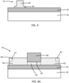
FIG. 2A is a cross-sectional view taken generally alongline 2A-2A inFIG. 1 . -
FIG. 3 is a top view of the structure at a fabrication stage of the processing method subsequent toFIGS. 1 ,2, 2A . -
FIG. 4 is a cross-sectional view taken generally along line 4-4 inFIG. 3 . -
FIG. 4A is a cross-sectional view taken generally alongline 4A-4A inFIG. 3 . -
FIG. 5 is a top view of the structure at a fabrication stage of the processing method subsequent toFIGS. 3 ,4, 4A . -
FIG. 6 is a cross-sectional view taken generally along line 6-6 inFIG. 5 . -
FIG. 6A is a cross-sectional view taken generally alongline 6A-6A inFIG. 5 . -
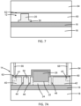
FIGS. 7, 7A are cross-sectional views of the structure at a fabrication stage of the processing method subsequent toFIGS. 5 ,6, 6A . -
FIGS. 8, 8A are cross-sectional views of structures in accordance with alternative embodiments of the invention. -
FIG. 9 is a top view of a structure in accordance with alternative embodiments of the invention. -
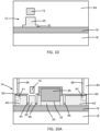
FIG. 10 is a cross-sectional view taken generally along line 10-10 inFIG. 9 . -
FIG. 10A is a cross-sectional view taken generally alongline 10A-10A inFIG. 9 . -
FIG. 11 is a top view of a structure in accordance with alternative embodiments of the invention. -
FIG. 12 is a top view of a structure in accordance with alternative embodiments of the invention. -
FIG. 13 is a top view of a structure in accordance with alternative embodiments of the invention. -
FIG. 14 is a top view of a structure in accordance with alternative embodiments of the invention. - With reference to
FIGS. 1 ,2, 2A and in accordance with embodiments of the invention, astructure 10 includes awaveguide core 12 and aphotodetector 14 that are positioned on, and above, adielectric layer 16 and asemiconductor substrate 18. In an embodiment, thedielectric layer 16 may be comprised of a dielectric material, such as silicon dioxide, and thesemiconductor substrate 18 may be comprised of a semiconductor material, such as single-crystal silicon. In an embodiment, thedielectric layer 16 may be disposed between thewaveguide core 12 and thesemiconductor substrate 18, and thedielectric layer 16 may be a buried oxide layer of a silicon-on-insulator substrate, and thedielectric layer 16 may provide low-index cladding for thewaveguide core 12 and thephotodetector 14. - The
waveguide core 12 includes asection 20 that is positioned adjacent to thephotodetector 14. Thesection 20, which extends lengthwise along alongitudinal axis 15, has asidewall 17 and asidewall 19 opposite from thesidewall 17. Thewaveguide core 12 may include aslab layer 30 that extends outwardly from each of thesidewalls slab layer 30 may be formed when thewaveguide core 12 is formed, and theslab layer 30 may have a thickness that is less than the thickness of thesection 20 of thewaveguide core 12. Theslab layer 30 is connected at each of thesidewalls section 20 of thewaveguide core 12. - The
photodetector 14 includes apad 24 having aside edge 23, aside edge 25 opposite from theside edge 23, aside edge 27, and aside edge 29 opposite from theside edge 27. Theside edges pad 24, and theside edges dielectric layer 16. In an embodiment, thesection 20 and theslab layer 30 of thewaveguide core 12 may be adjoined to theside edge 23 of thepad 24. - In an embodiment, the
waveguide core 12 and thepad 24 of thephotodetector 14 may be comprised of a material having a refractive index that is greater than the refractive index of silicon dioxide. In an embodiment, thewaveguide core 12 and thepad 24 of thephotodetector 14 may be comprised of a semiconductor material. In an embodiment, thewaveguide core 12 and thepad 24 of thephotodetector 14 may be comprised of single-crystal silicon. Thewaveguide core 12 and thepad 24 of thephotodetector 14 may be formed by patterning a layer comprised of their constituent material with lithography and etching processes. In an embodiment, thewaveguide core 12 and thepad 24 of thephotodetector 14 may be formed by patterning the semiconductor material (e.g., single-crystal silicon) of a device layer of a silicon-on-insulator substrate. - The
photodetector 14 further includes asemiconductor layer 26 providing a light-absorbing layer that is disposed on thepad 24 with an inward spacing from the outer perimeter of thepad 24. Thesemiconductor layer 26 extends lengthwise on thepad 24 along alongitudinal axis 36. Thesemiconductor layer 26 may have asidewall 34 that is positioned adjacent to theside edge 23 of thepad 24, asidewall 35 that is positioned adjacent to theside edge 25 of thepad 24, asidewall 37 that is positioned adjacent to theside edge 27 of thepad 24, and asidewall 39 that is positioned adjacent to theside edge 29 of thepad 24. In an embodiment, thesemiconductor layer 26 may be disposed equidistant from theside edge 27 and theside edge 29. Thesection 20 of thewaveguide core 12 is laterally offset along the side edge 32 from thelongitudinal axis 36 of thesemiconductor layer 26. In an embodiment, thesection 20 of thewaveguide core 12 may be laterally offset along theside edge 23 of thepad 24 between thesidewall 37 of thesemiconductor layer 26 and theside edge 27 of thepad 24. - The
semiconductor layer 26 of thephotodetector 14 may be comprised of a light-absorbing material that can generate charge carriers from photons of absorbed light by photoelectric conversion. In an embodiment, thesemiconductor layer 26 may be comprised of an intrinsic semiconductor material. In an embodiment, thesemiconductor layer 26 may be comprised of intrinsic germanium. In an embodiment, thesemiconductor layer 26 may be comprised of intrinsic silicon-germanium. In an alternative embodiment, thesemiconductor layer 26 may be comprised of a different type of semiconductor material, such as a III-V compound semiconductor material or intrinsic silicon. - The
semiconductor layer 26 may be formed by an epitaxial growth process. In an embodiment, thesemiconductor layer 26 may be epitaxially grown inside atrench 22 that is patterned in thepad 24 such that thesemiconductor layer 26 includes a lower portion disposed below atop surface 28 of thepad 24 and an upper portion disposed above thetop surface 28 of thepad 24. A hardmask comprised of a dielectric material may be disposed on thetop surface 28 of thepad 24 and surround thetrench 22 during the epitaxial growth process and may be removed following the epitaxial growth process. - With reference to
FIGS. 3 ,4, 4A in which like reference numerals refer to like features inFIGS. 1 ,2, 2A and at a subsequent fabrication stage, thestructure 10 may include a dopedregion 40 formed in a portion of thepad 24 adjacent to thesidewall 37 of thesemiconductor layer 26 and a dopedregion 42 that is formed in a portion of thepad 24 adjacent to thesidewall 39 of thesemiconductor layer 26. Thesemiconductor layer 26 is laterally positioned between the dopedregion 40 and the dopedregion 42. The dopedregions pad 24 to theunderlying dielectric layer 16. The dopedregion 40 and the dopedregion 42 may respectively define an anode and a cathode of thephotodetector 14. - The doped
region 40 may be formed by, for example, ion implantation with an implantation mask having an opening that determines the implanted area of thepad 24. The implantation mask may include a layer of photoresist applied by a spin-coating process, pre-baked, exposed to light projected through a photomask, baked after exposure, and developed with a chemical developer to define the opening over the area of thepad 24 to be implanted. The implantation conditions, such as ion species, dose, and kinetic energy, may be selected to tune the electrical and physical characteristics of the dopedregion 40. The implantation mask may be stripped after forming the dopedregion 40. In an embodiment, the semiconductor material of the dopedregion 40 may contain a p-type dopant, such as boron, that provides p-type electrical conductivity. In an alternative embodiment, a portion of thesemiconductor layer 26 immediately adjacent to the dopedregion 40 and an underlying portion of thepad 24 may be implanted with the p-type dopant due to partial overlap of the opening in the implantation mask with thesemiconductor layer 26. - The doped
region 42 may be formed by, for example, ion implantation with an implantation mask having an opening that determines an implanted area of thepad 24. The implantation mask may include a layer of photoresist applied by a spin-coating process, pre-baked, exposed to light projected through a photomask, baked after exposure, and developed with a chemical developer to define the opening over the area of thepad 24 to be implanted. The implantation conditions, such as ion species, dose, and kinetic energy, may be selected to tune the electrical and physical characteristics of the dopedregion 42. The implantation mask may be stripped after forming the dopedregion 42. In an embodiment, the semiconductor material of the dopedregion 42 may contain an n-type dopant, such as phosphorus or arsenic, that provides n-type electrical conductivity. In an alternative embodiment, a portion of thesemiconductor layer 26 immediately adjacent to the dopedregion 42 and an underlying portion of thepad 24 may be implanted with the n-type dopant due to overlap of the opening in the implantation mask. In an alternative embodiment, a portion of thesemiconductor layer 26 immediately adjacent to the dopedregion 42 and an underlying portion of thepad 24 may be implanted with the n-type dopant due to partial overlap of the opening in the implantation mask with thesemiconductor layer 26. - A portion of the
pad 24 beneath thesemiconductor layer 26 may be comprised of intrinsic semiconductor material, such as intrinsic silicon, that is not doped by the ion implantations forming thedoped regions pad 24 may extend beneath thesemiconductor layer 26 from theside edge 23 of thepad 24 to theside edge 25 of thepad 24. The dopedregion 40, the intrinsic semiconductor materials of thesemiconductor layer 26 and the portion of thepad 24 beneath thesemiconductor layer 26, and the dopedregion 42 may define a lateral p-i-n diode structure that enables the functionality of thephotodetector 14. - A heavily-doped
region 41 may be formed by a masked ion implantation in a portion of the dopedregion 40 adjacent to theside edge 27. A heavily-dopedregion 43 may be formed by a masked ion implantation in a portion of the dopedregion 42 adjacent to theside edge 29. The heavily-dopedregion 41 may have the same conductivity type as the dopedregion 40 but at a higher dopant concentration. The heavily-dopedregion 43 may have the same conductivity type as the dopedregion 42 but at a higher dopant concentration. - With reference to
FIGS. 5 ,6, 6A in which like reference numerals refer to like features inFIGS. 3 ,4, 4A and at a subsequent fabrication stage, atrench 44, atrench 46, and atrench 48 are formed that penetrate partially through thepad 24. Thetrenches pad 24. The lithography mask may include a layer of photoresist applied by a spin-coating process, pre-baked, exposed to light projected through a photomask, baked after exposure, and developed with a chemical developer to define openings over the areas of thepad 24 to be etched. In an embodiment, the etching process may be an anisotropic etching process. In an embodiment, the depth of thetrenches trench 22 holding thesemiconductor layer 26. For example, the depth of thetrenches trench 22 holding thesemiconductor layer 26. In an alternative embodiment, the depth of thetrenches trench 22 holding thesemiconductor layer 26. The thinned semiconductor material of the dopedregion 40 at the bottoms of the partially-etchedtrenches region 40 that couples the portion of thepad 24 beneath thesemiconductor layer 26 to the heavily-dopedregion 41. - The
trench 44 and thetrench 46 may be disposed in a spaced relationship on one side of thesemiconductor layer 26 between theside edge 27 of thepad 24 and thesidewall 37 of thesemiconductor layer 26. Thetrench 48 may be disposed on an opposite side of thesemiconductor layer 26 between theside edge 29 of thepad 24 and thesidewall 39 of thesemiconductor layer 26. In an embodiment, thetrenches side edge 23 of thepad 24. In an embodiment, thetrenches side edge 23 of thepad 24 in alignment with the portions of theslab layer 30 extending outwardly from theopposite sidewalls section 20 of thewaveguide core 12. In an embodiment, thetrenches side edge 25 of thepad 24 and thesidewall 35 of thesemiconductor layer 26. The spacing between thetrench 44 and thetrench 46 may decrease with increasing distance from theside edge 23 and decreasing distance from theside edge 25. - The portion of the semiconductor material of the
pad 24 between thetrench 44 and thetrench 46 defines awaveguide core 50 that is structurally and functionally integrated into thepad 24. Thewaveguide core 50 includes asidewall 53 and asidewall 55 opposite from thesidewall 53. Thesidewall 53 of thewaveguide core 50 is disposed adjacent to theside edge 27 of thepad 24 and thesidewall 55 of thewaveguide core 50 is disposed adjacent to thesidewall 37 of thesemiconductor layer 26. Thewaveguide core 50 has a top surface that is coplanar with thetop surface 28 of thepad 24. - The
waveguide core 50 provides an optical coupler configured to laterally transfer light received from thesection 20 of thewaveguide core 12 to thephotodetector 14. Thewaveguide core 50 is tapered with a width dimension W1 that decreases with increasing distance from theside edge 23 of thepad 24. The tapering of thewaveguide core 50 promotes the coupling of light from thewaveguide core 50 to thesemiconductor layer 26. Thesidewall 55 of thewaveguide core 50 is separated from thesidewall 37 of thesemiconductor layer 26 by a gap across which the light is laterally transferred. In an embodiment, the gap between thesidewall 55 of thewaveguide core 50 and thesidewall 37 of thesemiconductor layer 26 may be uniform with position between theside edge 23 of thepad 24 and theside edge 25 of thepad 24. In an alternative embodiment, the gap between thesidewall 55 of thewaveguide core 50 and thesidewall 37 of thesemiconductor layer 26 may vary with position between theside edge 23 of thepad 24 and theside edge 25 of thepad 24. - The
waveguide core 50 extends lengthwise along alongitudinal axis 52 that is inclined relative to thelongitudinal axis 36 of thesemiconductor layer 26. Thelongitudinal axis 52 of thewaveguide core 50 is laterally offset from thelongitudinal axis 36 of thesemiconductor layer 26. In an embodiment, thewaveguide core 50 may be laterally offset along theside edge 23 of thepad 24 between thesidewall 37 of thesemiconductor layer 26 and theside edge 27 of thepad 24. The lateral offset of thewaveguide core 50 compensates for the lateral offset of thesection 20 of thewaveguide core 12 and enables the lateral offset of thesection 20 of thewaveguide core 12. - With reference to
FIGS. 7, 7A in which like reference numerals refer to like features inFIGS. 5 ,6, 6A and at a subsequent fabrication stage, adielectric layer 60 is formed over thewaveguide core 12 and thephotodetector 14. In an embodiment, thedielectric layer 60 may be comprised of a dielectric material, such as silicon dioxide. The dielectric material of thedielectric layer 60 may fill thetrenches trenches waveguide core 50. The index contrast between the dielectric material in thetrenches waveguide core 50 enables the guided propagation of light in thewaveguide core 50 over a coupling region adjacent to thesemiconductor layer 26. - The dielectric material in the
trench 48 provides an index contrast with the semiconductor material of thepad 24 that permits thetrench 48 to function as a mode confiner that improves light coupling to thesemiconductor layer 26. In that regard, the mode confinement provided by thetrench 48 and the dielectric material in thetrench 48 may push the electromagnetic field associated with the light guided by thewaveguide core 50 toward thesemiconductor layer 26. In an alternative embodiment, thetrench 48 may be omitted from thestructure 10. - A
conformal dielectric layer 62 may be formed that extends across thewaveguide core 12 andphotodetector 14 and that follows the topography created by thesemiconductor layer 26. In an embodiment, theconformal dielectric layer 62 may be comprised of a dielectric material, such as silicon nitride. Adielectric layer 64 may be formed on theconformal dielectric layer 62. In an embodiment, thedielectric layer 64 may be comprised of a dielectric material, such as silicon dioxide, that has a lower refractive index than the material of thewaveguide core 12. Thedielectric layer 64 may be deposited and planarized by chemical-mechanical polishing. -
Contacts 66 may be formed that penetrate fully through thedielectric layers region 41, andcontacts 68 may be formed that penetrate fully through thedielectric layers region 43. The heavily-dopedregion 41 electrically couples thecontacts 66 to the dopedregion 40 with a reduced contact resistance. The heavily-dopedregion 43 electrically couples thecontacts 68 to the dopedregion 42 with a reduced contact resistance. Thecontacts regions contacts dielectric layer 64. - In use, light, such as laser light, propagates in the
waveguide core 12 toward thephotodetector 14 and is transferred at theside edge 23 of thepad 24 from thesection 20 of thewaveguide core 12 to thewaveguide core 50. Thewaveguide core 12 andwaveguide core 50 may support propagation of light with transverse-electric polarization, transverse-magnetic polarization, or a combination of both polarizations. Light guided by thewaveguide core 50 is then laterally coupled by thewaveguide core 50 to thesemiconductor layer 26 of thephotodetector 14. In an embodiment, the light received by thephotodetector 14 may be modulated as an optical signal. Thesemiconductor layer 26 absorbs photons of the laterally-transferred light and converts the absorbed photons into charge carriers by photoelectric conversion. The biasing of the dopedregions photodetector 14 to provide, as a function of time, a measurable photocurrent. - The
waveguide core 50 integrated into thesemiconductor layer 26 may function as a mode-evolution-based optical coupler that improves the responsivity of thephotodetector 14. The improvement in responsivity of thephotodetector 14, particularly at high optical powers, may provide a significant improvement in system level performance. - With reference to
FIGS. 8, 8A and in accordance with alternative embodiments, thestructure 10 may be modified such that thephotodetector 14 has a vertical arrangement instead of a lateral arrangement. Specifically, as shown inFIG. 8 , the dopedregion 40 may be extend across theentire pad 24, heavily-dopedregions 41 may be disposed in thepad 24 on both sides of thesemiconductor layer 26, and the dopedregion 42 and heavily-dopedregion 43 may be disposed in an upper portion of thesemiconductor layer 26. In an alternative embodiment and as shown inFIG. 8A , thestructure 10 may be configured with a heavily-dopedregion 41 disposed in thepad 24 adjacent to only one side of thesemiconductor layer 26. - In an alternative embodiment, the
semiconductor layer 26 may be fully disposed on, and above, thetop surface 28 of thepad 24. In an alternative embodiment, thephotodetector 14 may be configured as an avalanche photodetector that includes a region of intrinsic semiconductor material in thepad 24 defining a multiplication region and an additional doped region in thepad 24 defining a charge control region. - With reference to
FIGS. 9 ,10, 10A and in accordance with alternative embodiments, thestructure 10 may further include awaveguide core 70 that is disposed in elevation over thewaveguide core 50 to define a stacked waveguiding structure. Thestructure 10 may also further include awaveguide core 72 that is disposed in elevation over at least thesection 20 of thewaveguide core 12 to define a stacked waveguiding structure. In an embodiment, thewaveguide cores waveguide core 12 and thewaveguide core 50. In an embodiment, thewaveguide cores waveguide cores - In an embodiment, the
waveguide core 72 may be narrower than thewaveguide core 12 and centered above thewaveguide core 12 with intervening dielectric material. A section of thedielectric layer 62 may be removed from the region between thewaveguide core 70 and thewaveguide core 12. Thewaveguide core 70 may be narrower than thewaveguide core 50 and centered above thewaveguide core 50 with intervening dielectric material. In an embodiment, the width dimension of thewaveguide core 70 may taper in coordination with the tapering of thewaveguide core 50. For example, thewaveguide core 70 may taper at the same taper angle or set of taper angles as thewaveguide core 50. - With reference to
FIG. 11 and in accordance with alternative embodiments, thestructure 10 may further include awaveguide core 13 having asection 21 that is positioned adjacent to thephotodetector 14. Thesection 21 may have aslab layer 31 that extends outwardly from each of its opposite sidewalls. Thewaveguide core 13, thesection 21 of thewaveguide core 13, and theslab layer 31 may be respectively similar or identical in construction to thewaveguide core 12, thesection 20 of thewaveguide core 12, and theslab layer 30. Thesection 21 andslab layer 31 of thewaveguide core 13 may adjoin theside edge 23 of thepad 24. Thesection 21 of thewaveguide core 13 may be disposed along theside edge 23 of thepad 24 on an opposite side of thesemiconductor layer 26 from thesection 20 of thewaveguide core 12. In an embodiment, thewaveguide core 13 may be comprised of the same material as thewaveguide core 12 and thepad 24 of thephotodetector 14, and theslab layer 31 may be comprised of the same material as theslab layer 30. - The
structure 10 may also include atrench 49 that penetrates partially through thepad 24. Thetrench 49 may be formed by lithography and etching processes when thetrenches trench 49 is disposed on the same side of thesemiconductor layer 26 as thetrench 48. Thetrench 48 is disposed between thetrench 49 and thesidewall 39 of thesemiconductor layer 26, and thetrench 49 is disposed between thetrench 48 and theside edge 29 of thepad 24. In an embodiment, thetrench 49 may intersect theside edge 23 of thepad 24. In an embodiment, thetrenches side edge 23 of thepad 24 in alignment with the portions of theslab layer 31 extending outwardly from the opposite sidewalls of thesection 21 of thewaveguide core 13. In an embodiment, thetrench 49 may also terminate at an end adjacent to theside edge 25 of thepad 24 and thesidewall 35 of thesemiconductor layer 26. - The portion of the
pad 24 between thetrench 48 and thetrench 49 defines awaveguide core 51 that is structurally and functionally integrated into thepad 24. Thewaveguide core 51 includes a sidewall disposed adjacent to theside edge 29 of thepad 24 and a sidewall disposed adjacent to thesidewall 39 of thesemiconductor layer 26. The thinned material of the dopedregion 42 at the bottom of the partially-etchedtrenches region 42 connecting the portion of thepad 24 beneath thesemiconductor layer 26 and the heavily-dopedregion 43. - The
waveguide core 51 provides an optical coupler configured to laterally transfer light received from thesection 21 of thewaveguide core 13 to thephotodetector 14. Thewaveguide core 51 is tapered with a width dimension W2 that decreases with increasing distance from theside edge 23 of thepad 24. The tapering of thewaveguide core 51 promotes light transfer from thewaveguide core 51 to thesemiconductor layer 26 of thephotodetector 14. A sidewall of thewaveguide core 51 is separated from theadjacent sidewall 39 of thesemiconductor layer 26 by a gap that may be uniform with position between theside edge 23 of thepad 24 and theside edge 25 of thepad 24 or that may vary with position between theside edge 23 of thepad 24 and theside edge 25 of thepad 24. - The
waveguide core 51 is laterally offset from thelongitudinal axis 36 of thesemiconductor layer 26. In an embodiment, thewaveguide core 51 may be laterally offset along theside edge 23 of thepad 24 between thesidewall 39 of thesemiconductor layer 26 and theside edge 29 of thepad 24. The lateral offset of thewaveguide core 51 compensates for the lateral offset of thesection 21 of thewaveguide core 13 and enables the lateral offset of thesection 21 of thewaveguide core 13. Similar to thewaveguide core 50, thewaveguide core 51 has a longitudinal axis that is inclined relative to thelongitudinal axis 36 of thesemiconductor layer 26. - The
section 21 of thewaveguide core 13 and thewaveguide core 51 supply another input to thephotodetector 14 in addition to the input provided by thesection 20 of thewaveguide core 12 and thewaveguide core 50. The total optical power delivered to thephotodetectors 14 may be split between the different inputs, which may further improve the responsivity of thephotodetector 14 and system level performance, particularly at high optical powers. - With reference to
FIG. 12 and in accordance with alternative embodiments, thesection 21 of thewaveguide core 13 may adjoin theside edge 25 of thepad 24 instead of theside edge 23, and thetrench 49 may be inclined in an opposite direction to form thewaveguide core 51 with a taper that is opposite in width dimension change to the tapering of thewaveguide core 50. Thesection 21 of thewaveguide core 13 and thewaveguide core 51 supply another input to thephotodetector 14, in addition to the input provided by thesection 20 of thewaveguide core 12 and thewaveguide core 50, with thephotodetector 14 disposed between the different inputs. - With reference to
FIG. 13 and in accordance with alternative embodiments, thestructure 10 may also includetrenches pad 24. Thetrenches trenches trenches semiconductor layer 26 as thetrench 48, and thetrenches dielectric layer 60. Thetrenches trenches trenches trench 48, function to further strengthen and reinforce mode confinement and to further improve light coupling to thesemiconductor layer 26. - With reference to
FIG. 14 and in accordance with alternative embodiments,trenches 58 may be formed that are arranged in the rows and columns of a two-dimensional array. Thetrenches 58 may be formed by lithography and etching processes when thetrenches trenches 58 are disposed on an opposite side of thesemiconductor layer 26 from thetrenches dielectric layer 60. The dielectric material in thetrenches 58 provides an index contrast with the semiconductor material of thepad 24 and permits the dielectric-filledtrenches 58 to provide mode confinement and to improve light coupling to thesemiconductor layer 26. - The methods as described above are used in the fabrication of integrated circuit chips. The resulting integrated circuit chips can be distributed by the fabricator in raw wafer form (e.g., as a single wafer that has multiple unpackaged chips), as a bare die, or in a packaged form. The chip may be integrated with other chips, discrete circuit elements, and/or other signal processing devices as part of either an intermediate product or an end product. The end product can be any product that includes integrated circuit chips, such as computer products having a central processor or smartphones.
- References herein to terms modified by language of approximation, such as "about", "approximately", and "substantially", are not to be limited to the precise value specified. The language of approximation may correspond to the precision of an instrument used to measure the value and, unless otherwise dependent on the precision of the instrument, may indicate a range of +/- 10% of the stated value(s).
- References herein to terms such as "vertical", "horizontal", etc. are made by way of example, and not by way of limitation, to establish a frame of reference. The term "horizontal" as used herein is defined as a plane parallel to a conventional plane of a semiconductor substrate, regardless of its actual three-dimensional spatial orientation. The terms "vertical" and "normal" refer to a direction in the frame of reference perpendicular to the horizontal, as just defined. The term "lateral" refers to a direction in the frame of reference within the horizontal plane.
- A feature "connected" or "coupled" to or with another feature may be directly connected or coupled to or with the other feature or, instead, one or more intervening features may be present. A feature may be "directly connected" or "directly coupled" to or with another feature if intervening features are absent. A feature may be "indirectly connected" or "indirectly coupled" to or with another feature if at least one intervening feature is present. A feature "on" or "contacting" another feature may be directly on or in direct contact with the other feature or, instead, one or more intervening features may be present. A feature may be "directly on" or in "direct contact" with another feature if intervening features are absent. A feature may be "indirectly on" or in "indirect contact" with another feature if at least one intervening feature is present. Different features "overlap" if a feature extends over, and covers a part of, another feature.
- The descriptions of the various embodiments of the present invention have been presented for purposes of illustration but are not intended to be exhaustive or limited to the embodiments disclosed. Many modifications and variations will be apparent to those of ordinary skill in the art without departing from the scope and spirit of the described embodiments. The terminology used herein was chosen to best explain the principles of the embodiments, the practical application or technical improvement over technologies found in the marketplace, or to enable others of ordinary skill in the art to understand the embodiments disclosed herein.
- In summary, structures for a photonics chip that include a photodetector and methods of forming such structures are disclosed. The structure comprises a photodetector including a pad and a semiconductor layer on the pad. The pad includes a side edge and a first waveguide core that extends from the side edge adjacent to the semiconductor layer. The structure further comprises a second waveguide core including a section adjoined to the side edge of the pad adjacent to the first waveguide core.
- The following embodiments are explicitly disclosed.
- A structure for a photonics chip, the structure comprising:
- a photodetector including a pad and a semiconductor layer on the pad, the pad including a first side edge and a first waveguide core that extends from the first side edge adjacent to the semiconductor layer; and
- a second waveguide core including a section adjoined to the first side edge of the pad adjacent to the first waveguide core.
- The structure of embodiment 1, wherein the semiconductor layer has a longitudinal axis, and the first waveguide core is laterally offset along the first side edge relative to the longitudinal axis of the semiconductor layer.
- The structure of
embodiment 1 or 2, wherein the pad includes a first trench and a second trench, and the first waveguide core is disposed between the first trench and the second trench. Embodiment 4:
The structure of embodiment 3, wherein the first trench and the second trench penetrate partially through a thickness of the pad. - The structure of
embodiment 3 or 4, wherein the first waveguide core comprises a semiconductor material having a first refractive index, and the first trench and the second trench are filled by a dielectric material having a second refractive index that is less than the first refractive index. - The structure of embodiment 5, wherein the pad comprises the semiconductor material.
- The structure of one of embodiments 3 to 6, wherein the semiconductor layer includes a first sidewall adjacent to the first waveguide core and a second sidewall, the first trench and the second trench are disposed adjacent to the first sidewall, and the pad includes a third trench disposed adjacent to the second sidewall.
- The structure of
embodiment 7, wherein the first waveguide core comprises a semiconductor material having a first refractive index, and the first trench, the second trench, and the third trench are filled by a dielectric material having a second refractive index that is less than the first refractive index. - The structure of
embodiment 7 or 8, wherein the pad includes a fourth trench disposed between the second sidewall and the third trench. - The structure of one of embodiments 3 to 9, wherein the semiconductor layer includes a first sidewall adjacent to the first waveguide core and a second sidewall, the first trench and the second trench are disposed adjacent to the first sidewall, and the pad includes a plurality of trenches disposed in a two-dimensional array adjacent to the second sidewall.
- The structure of one of embodiments 1 to 10, wherein the second waveguide core is aligned with the first waveguide core at the first side edge of the pad.
- The structure of one of embodiments 1 to 11, wherein the second waveguide core includes a slab layer.
- The structure of one of embodiments 1 to 12, wherein the semiconductor layer has a longitudinal axis, and the first waveguide core includes a longitudinal axis that is inclined relative to the longitudinal axis of the semiconductor layer.
- The structure of one of embodiments 1 to 13, wherein the pad includes a third waveguide core that extends from the first side edge adjacent to the semiconductor layer, and further comprising:
a fourth waveguide core including a section adjoined to the first side edge of the pad adjacent to the third waveguide core. - The structure of
embodiment 14, wherein the semiconductor layer is disposed between the first waveguide core and the third waveguide core, the semiconductor layer has a longitudinal axis, and the third waveguide core includes a longitudinal axis that is inclined relative to the longitudinal axis of the semiconductor layer. - The structure of one of embodiments 1 to 15, wherein the pad includes a second side edge opposite from the first side edge and a third waveguide core that extends from the second side edge adjacent to the semiconductor layer, and further comprising:
a fourth waveguide core including a section adjoined to the second side edge of the pad. - The structure of
embodiment 16, wherein the semiconductor layer is disposed between the first waveguide core and the third waveguide core, the semiconductor layer has a longitudinal axis, and the third waveguide core includes a longitudinal axis that is inclined relative to the longitudinal axis of the semiconductor layer. - The structure of one of embodiments 1 to 17, further comprising:
- a third waveguide core disposed over the first waveguide core,
- wherein the first waveguide core comprises a first material, and the third waveguide core comprises a second material different from the first material.
- The structure of one of embodiments 1 to 18, further comprising:
- a first doped region in the pad, the first doped region having a first conductivity type; and
- a second doped region in the pad, the second doped region having a second conductivity type opposite to the first conductivity type,
- wherein the semiconductor layer is disposed on a portion of the pad between the first doped region and the second doped region, and the portion of the pad comprises intrinsic semiconductor material.
- A method of forming a structure for a photonics chip, the method comprising:
- forming a photodetector that includes a pad and a semiconductor layer on the pad, wherein the pad includes a side edge and a first waveguide core that extends from the side edge adjacent to the semiconductor layer; and
- forming a second waveguide core that includes a section adjoined to the side edge of the pad adjacent to the first waveguide core.
- At least in the embodiments above, the term "include" and its variants may be interpreted as meaning that an embodiment includes stated features, while not necessarily excluding the presence of other features that are not explicitly stated.
- The method of
embodiment 20, wherein the structure of one of embodiments 1 to 19 is formed.
Claims (15)
- A structure for a photonics chip, the structure comprising:a photodetector including a pad and a semiconductor layer on the pad, the pad including a first side edge and a first waveguide core that extends from the first side edge adjacent to the semiconductor layer; anda second waveguide core including a section adjoined to the first side edge of the pad adjacent to the first waveguide core.
- The structure of claim 1, wherein the semiconductor layer has a longitudinal axis, and the first waveguide core is laterally offset along the first side edge relative to the longitudinal axis of the semiconductor layer.
- The structure of claim 1 or 2, wherein the pad includes a first trench and a second trench, and the first waveguide core is disposed between the first trench and the second trench.
- The structure of claim 3, wherein the first trench and the second trench penetrate partially through a thickness of the pad, and/or
wherein the semiconductor layer includes a first sidewall adjacent to the first waveguide core and a second sidewall, the first trench and the second trench being disposed adjacent to the first sidewall and the pad including a plurality of trenches disposed in a two-dimensional array adjacent to the second sidewall. - The structure of claim 3 or 4, wherein the first waveguide core comprises a semiconductor material having a first refractive index, and the first trench and the second trench are filled by a dielectric material having a second refractive index that is less than the first refractive index, the pad preferably comprising the semiconductor material; and
- The structure of one of claims 3 to 5, wherein the semiconductor layer includes a first sidewall adjacent to the first waveguide core and a second sidewall, the first trench and the second trench are disposed adjacent to the first sidewall, and the pad includes a third trench disposed adjacent to the second sidewall.
- The structure of claim 6, wherein the first waveguide core comprises a semiconductor material having a first refractive index, and the first trench, the second trench, and the third trench are filled by a dielectric material having a second refractive index that is less than the first refractive index, and/or
wherein the pad includes a fourth trench disposed between the second sidewall and the third trench. - The structure of one of claims 1 to 7, wherein the second waveguide core is aligned with the first waveguide core at the first side edge of the pad; and/orwherein the second waveguide core includes a slab layer; and/orwherein the semiconductor layer has a longitudinal axis, and the first waveguide core includes a longitudinal axis that is inclined relative to the longitudinal axis of the semiconductor layer.
- The structure of one of claims 1 to 8, wherein the pad includes a third waveguide core that extends from the first side edge adjacent to the semiconductor layer, and further comprising:
a fourth waveguide core including a section adjoined to the first side edge of the pad adjacent to the third waveguide core. - The structure of claim 9, wherein the semiconductor layer is disposed between the first waveguide core and the third waveguide core, the semiconductor layer has a longitudinal axis, and the third waveguide core includes a longitudinal axis that is inclined relative to the longitudinal axis of the semiconductor layer.
- The structure of one of claims 1 to 10, wherein the pad includes a second side edge opposite from the first side edge and a third waveguide core that extends from the second side edge adjacent to the semiconductor layer, and further comprising:
a fourth waveguide core including a section adjoined to the second side edge of the pad. - The structure of claim 11, wherein the semiconductor layer is disposed between the first waveguide core and the third waveguide core, the semiconductor layer has a longitudinal axis, and the third waveguide core includes a longitudinal axis that is inclined relative to the longitudinal axis of the semiconductor layer.
- The structure of one of claims 1 to 12, further comprising at least one of:a third waveguide core disposed over the first waveguide core, wherein the first waveguide core comprises a first material, and the third waveguide core comprises a second material different from the first material; anda first doped region in the pad and a second doped region in the pad, the first doped region having a first conductivity type and the second doped region having a second conductivity type opposite to the first conductivity type, wherein the semiconductor layer is disposed on a portion of the pad between the first doped region and the second doped region, and the portion of the pad comprises intrinsic semiconductor material.
- A method of forming a structure for a photonics chip, the method comprising:forming a photodetector that includes a pad and a semiconductor layer on the pad, wherein the pad includes a side edge and a first waveguide core that extends from the side edge adjacent to the semiconductor layer; andforming a second waveguide core that includes a section adjoined to the side edge of the pad adjacent to the first waveguide core.
- The method of claim 14, wherein the structure of one of claims 1 to 13 is formed.
Applications Claiming Priority (1)
| Application Number | Priority Date | Filing Date | Title |
|---|---|---|---|
| US18/405,727 US20250224578A1 (en) | 2024-01-05 | 2024-01-05 | Photodetectors with an integrated waveguide core |
Publications (1)
| Publication Number | Publication Date |
|---|---|
| EP4582843A1 true EP4582843A1 (en) | 2025-07-09 |
Family
ID=91898742
Family Applications (1)
| Application Number | Title | Priority Date | Filing Date |
|---|---|---|---|
| EP24187696.0A Pending EP4582843A1 (en) | 2024-01-05 | 2024-07-10 | Photodetectors with an integrated waveguide core |
Country Status (3)
| Country | Link |
|---|---|
| US (1) | US20250224578A1 (en) |
| EP (1) | EP4582843A1 (en) |
| CN (1) | CN120282588A (en) |
Cited By (1)
| Publication number | Priority date | Publication date | Assignee | Title |
|---|---|---|---|---|
| EP4660673A1 (en) * | 2024-04-30 | 2025-12-10 | Ranovus Inc. | Photodiodes with carrier screening mitigation |
Citations (4)
| Publication number | Priority date | Publication date | Assignee | Title |
|---|---|---|---|---|
| US20190280144A1 (en) * | 2018-03-07 | 2019-09-12 | Stmicroelectronics (Crolles 2) Sas | Vertical photodiode |
| US20210313306A1 (en) * | 2017-06-08 | 2021-10-07 | Luxtera Llc | Method and system for selectively illluminated integrated photodetectors with configured launching and adaptive junction profile for bandwidth improvement |
| US20220283391A1 (en) * | 2021-03-08 | 2022-09-08 | Alpine Optoelectronics, Inc. | Integrated germanium photodetector with silicon nitride launch waveguide |
| US20230042376A1 (en) * | 2019-12-27 | 2023-02-09 | Wuhan Optical Valley Information Optoelectronics Innovation Center Co., Ltd | Photoelectric detector |
Family Cites Families (1)
| Publication number | Priority date | Publication date | Assignee | Title |
|---|---|---|---|---|
| US11199672B1 (en) * | 2020-06-15 | 2021-12-14 | Globalfoundries U.S. Inc. | Multiple waveguide coupling to one or more photodetectors |
-
2024
- 2024-01-05 US US18/405,727 patent/US20250224578A1/en active Pending
- 2024-07-10 EP EP24187696.0A patent/EP4582843A1/en active Pending
- 2024-12-05 CN CN202411779742.9A patent/CN120282588A/en active Pending
Patent Citations (4)
| Publication number | Priority date | Publication date | Assignee | Title |
|---|---|---|---|---|
| US20210313306A1 (en) * | 2017-06-08 | 2021-10-07 | Luxtera Llc | Method and system for selectively illluminated integrated photodetectors with configured launching and adaptive junction profile for bandwidth improvement |
| US20190280144A1 (en) * | 2018-03-07 | 2019-09-12 | Stmicroelectronics (Crolles 2) Sas | Vertical photodiode |
| US20230042376A1 (en) * | 2019-12-27 | 2023-02-09 | Wuhan Optical Valley Information Optoelectronics Innovation Center Co., Ltd | Photoelectric detector |
| US20220283391A1 (en) * | 2021-03-08 | 2022-09-08 | Alpine Optoelectronics, Inc. | Integrated germanium photodetector with silicon nitride launch waveguide |
Cited By (1)
| Publication number | Priority date | Publication date | Assignee | Title |
|---|---|---|---|---|
| EP4660673A1 (en) * | 2024-04-30 | 2025-12-10 | Ranovus Inc. | Photodiodes with carrier screening mitigation |
Also Published As
| Publication number | Publication date |
|---|---|
| CN120282588A (en) | 2025-07-08 |
| US20250224578A1 (en) | 2025-07-10 |
Similar Documents
| Publication | Publication Date | Title |
|---|---|---|
| KR101721343B1 (en) | Method and apparatus for reducing signal loss in a photo detector | |
| US12272758B2 (en) | Photodetectors and absorbers with slanted light incidence | |
| US11588062B2 (en) | Photodetectors including a coupling region with multiple tapers | |
| US11199672B1 (en) | Multiple waveguide coupling to one or more photodetectors | |
| US20250006856A1 (en) | Diode with light-sensitive intrinsic region | |
| US20260140311A1 (en) | Photonic components with chamfered sidewalls | |
| US11609377B2 (en) | Photodetectors and terminators having a curved shape | |
| CA2771346A1 (en) | Optical device having light sensor employing horizontal electrical field | |
| US11520113B1 (en) | Photodetectors and terminators including a tapered thickness | |
| US20250224578A1 (en) | Photodetectors with an integrated waveguide core | |
| EP4390479A1 (en) | Photodetectors with a tapered interface | |
| EP4550015A1 (en) | Photodetectors with a notched light-absorbing layer | |
| US20110310467A1 (en) | System having light sensor with enhanced sensitivity | |
| CN116263521B (en) | Photodetector integrated with an anti-cone shape including a curved end | |
| US20250189721A1 (en) | Photonics chips including a photonic coupler and a photodetector | |
| EP4585980A1 (en) | Photodetectors with an adjoined slotted waveguiding structure | |
| US12321009B1 (en) | Photodetectors with multiple light-absorbing semiconductor layers | |
| US12557431B2 (en) | Photodetectors with a light-absorbing layer at least partially wrapped about a waveguide core | |
| US20240395965A1 (en) | Photodetectors with one or more confining features | |
| EP4462165A2 (en) | Photodetectors integrated with a segmented coupling-assistance feature | |
| EP4707883A1 (en) | Photodetectors with an integrated grating coupler | |
| US20260090115A1 (en) | Photonic chips including a hybrid plasmonic photodetector | |
| EP4682601A1 (en) | Photonic chips including a photonic component and delay lines |
Legal Events
| Date | Code | Title | Description |
|---|---|---|---|
| PUAI | Public reference made under article 153(3) epc to a published international application that has entered the european phase |
Free format text: ORIGINAL CODE: 0009012 |
|
| STAA | Information on the status of an ep patent application or granted ep patent |
Free format text: STATUS: REQUEST FOR EXAMINATION WAS MADE |
|
| 17P | Request for examination filed |
Effective date: 20240710 |
|
| AK | Designated contracting states |
Kind code of ref document: A1 Designated state(s): AL AT BE BG CH CY CZ DE DK EE ES FI FR GB GR HR HU IE IS IT LI LT LU LV MC ME MK MT NL NO PL PT RO RS SE SI SK SM TR |