EP4582838A1 - Detection apparatus, radiation identification apparatus, and neutron imaging apparatus - Google Patents
Detection apparatus, radiation identification apparatus, and neutron imaging apparatus Download PDFInfo
- Publication number
- EP4582838A1 EP4582838A1 EP23860523.2A EP23860523A EP4582838A1 EP 4582838 A1 EP4582838 A1 EP 4582838A1 EP 23860523 A EP23860523 A EP 23860523A EP 4582838 A1 EP4582838 A1 EP 4582838A1
- Authority
- EP
- European Patent Office
- Prior art keywords
- electron
- detecting apparatus
- anode
- signal
- data
- Prior art date
- Legal status (The legal status is an assumption and is not a legal conclusion. Google has not performed a legal analysis and makes no representation as to the accuracy of the status listed.)
- Pending
Links
Images








Classifications
-
- G—PHYSICS
- G01—MEASURING; TESTING
- G01T—MEASUREMENT OF NUCLEAR OR X-RADIATION
- G01T1/00—Measuring X-radiation, gamma radiation, corpuscular radiation, or cosmic radiation
- G01T1/16—Measuring radiation intensity
- G01T1/17—Circuit arrangements not adapted to a particular type of detector
-
- G—PHYSICS
- G01—MEASURING; TESTING
- G01T—MEASUREMENT OF NUCLEAR OR X-RADIATION
- G01T1/00—Measuring X-radiation, gamma radiation, corpuscular radiation, or cosmic radiation
- G01T1/16—Measuring radiation intensity
- G01T1/185—Measuring radiation intensity with ionisation chamber arrangements
-
- G—PHYSICS
- G01—MEASURING; TESTING
- G01T—MEASUREMENT OF NUCLEAR OR X-RADIATION
- G01T1/00—Measuring X-radiation, gamma radiation, corpuscular radiation, or cosmic radiation
- G01T1/16—Measuring radiation intensity
- G01T1/18—Measuring radiation intensity with counting-tube arrangements, e.g. with Geiger counters
-
- G—PHYSICS
- G01—MEASURING; TESTING
- G01T—MEASUREMENT OF NUCLEAR OR X-RADIATION
- G01T1/00—Measuring X-radiation, gamma radiation, corpuscular radiation, or cosmic radiation
- G01T1/16—Measuring radiation intensity
- G01T1/20—Measuring radiation intensity with scintillation detectors
-
- G—PHYSICS
- G01—MEASURING; TESTING
- G01T—MEASUREMENT OF NUCLEAR OR X-RADIATION
- G01T1/00—Measuring X-radiation, gamma radiation, corpuscular radiation, or cosmic radiation
- G01T1/16—Measuring radiation intensity
- G01T1/24—Measuring radiation intensity with semiconductor detectors
-
- G—PHYSICS
- G01—MEASURING; TESTING
- G01T—MEASUREMENT OF NUCLEAR OR X-RADIATION
- G01T1/00—Measuring X-radiation, gamma radiation, corpuscular radiation, or cosmic radiation
- G01T1/29—Measurement performed on radiation beams, e.g. position or section of the beam; Measurement of spatial distribution of radiation
- G01T1/2914—Measurement of spatial distribution of radiation
- G01T1/2921—Static instruments for imaging the distribution of radioactivity in one or two dimensions; Radio-isotope cameras
- G01T1/2935—Static instruments for imaging the distribution of radioactivity in one or two dimensions; Radio-isotope cameras using ionisation detectors
-
- G—PHYSICS
- G01—MEASURING; TESTING
- G01T—MEASUREMENT OF NUCLEAR OR X-RADIATION
- G01T3/00—Measuring neutron radiation
-
- G—PHYSICS
- G01—MEASURING; TESTING
- G01T—MEASUREMENT OF NUCLEAR OR X-RADIATION
- G01T3/00—Measuring neutron radiation
- G01T3/008—Measuring neutron radiation using an ionisation chamber filled with a gas, liquid or solid, e.g. frozen liquid, dielectric
Definitions
- An embodiment of the present disclosure relates to a detecting apparatus that detects an electron, a radiation identification apparatus, and a neutron imaging apparatus.
- the detecting apparatus includes a container in which gas is contained, an electron detector that detects an electron produced by Compton scattering, and a radiation detector that detects radiation scattered by Compton scattering.
- Data regarding an electron detected by the electron detector is useful for analyzing radiation. For example, as described in PTL 1, information about the scattering direction of radiation is calculated from information about the position of the radiation detected by the radiation detector and information about the point of origin of the electron.
- Data detected by the electron detector is transmitted to the computer.
- the computer is under heavy load.
Landscapes
- Physics & Mathematics (AREA)
- Health & Medical Sciences (AREA)
- Life Sciences & Earth Sciences (AREA)
- General Physics & Mathematics (AREA)
- High Energy & Nuclear Physics (AREA)
- Molecular Biology (AREA)
- Spectroscopy & Molecular Physics (AREA)
- Measurement Of Radiation (AREA)
Abstract
Description
- An embodiment of the present disclosure relates to a detecting apparatus that detects an electron, a radiation identification apparatus, and a neutron imaging apparatus.
- As disclosed in, for example,
PTLs 1 to 3, there is known a detecting apparatus that detects Compton-scattered radiation and an electron produced by Compton scattering. The detecting apparatus includes a container in which gas is contained, an electron detector that detects an electron produced by Compton scattering, and a radiation detector that detects radiation scattered by Compton scattering. - Data regarding an electron detected by the electron detector is useful for analyzing radiation. For example, as described in
PTL 1, information about the scattering direction of radiation is calculated from information about the position of the radiation detected by the radiation detector and information about the point of origin of the electron. -
- PTL 1:
Japanese Unexamined Patent Application Publication No. 2015-148448 - PTL 2:
Japanese Unexamined Patent Application Publication No. 2016-161522 - PTL 3: International Publication No.
2017/209059 - Data detected by the electron detector is transmitted to the computer. When all the data detected by the electron detector is transmitted to the computer, the computer is under heavy load.
- The embodiment of the present disclosure aims to provide a detecting apparatus that can effectively solve such problems.
- The embodiment of the present disclosure relates to the following [1] to [18].
- [1] A detecting apparatus that detects an electron includes:
- a container containing gas;
- an electron detector located inside the container, the electron detector detecting an electron of an electron cloud formed inside the container to generate an analog signal;
- a drift electrode facing the electron detector;
- a second read circuit digitizing the analog signal generated by the electron detector to generate second data; and
- a computer capable of communicating with the second read circuit, wherein
- the second read circuit includes a second buffer in which the second data is stored, and
- the second read circuit transmits second final data including the second data stored in the second buffer to the computer in response to a second trigger signal.
- [2] In the detecting apparatus according to [1], the detecting apparatus may include a logic circuit connected to the second read circuit, the second read circuit may generate a second hit signal when an intensity of the analog signal of the electron detector exceeds a threshold, and the logic circuit may generate the second trigger signal after a second delay time has elapsed since generation of the second hit signal in the electron detector.
- [3] In the detecting apparatus according to [1], the detecting apparatus may include a logic circuit connected to the second read circuit, the electron detector may include a plurality of anode electrodes and a plurality of cathode electrodes, the analog signal of the electron detector may include anode analog signals generated by the plurality of anode electrodes and cathode analog signals generated by the plurality of cathode electrodes, the second read circuit may generate an anode hit signal when an intensity of the anode analog signal exceeds a threshold, and may generate a cathode hit signal when an intensity of the cathode analog signal exceeds a threshold, and the logic circuit may generate the second trigger signal in response to generation of both the anode hit signal and the cathode hit signal.
- [4] In the detecting apparatus according to [3], the detecting apparatus may include a logic circuit connected to the second read circuit, and the logic circuit may generate the second trigger signal after a second delay time has elapsed since generation of both the anode hit signal and the cathode hit signal.
- [5] In the detecting apparatus according to [2] or [4], the second delay time may be shorter than or equal to a maximum travel time, and the maximum travel time may be a time taken for an electron to travel from the drift electrode to the electron detector.
- [6] In the detecting apparatus according to [2], [4], or [5], the second buffer of the second read circuit may store the second data during a second storage period, and the second storage period may be longer than or equal to the second delay time.
- [7] In the detecting apparatus according to any one of [1] to [6], the second final data may include information about an intensity of the analog signal generated by the electron detector.
- [8] In the detecting apparatus according to [7], the second read circuit may acquire information about the intensity of the analog signal generated by the electron detector at a sampling frequency of lower than or equal to 50 MHz.
- [9] In the detecting apparatus according to [7], the second read circuit may acquire information about the intensity of the analog signal generated by the electron detector at a sampling frequency of higher than or equal to 10 MHz and lower than or equal to 20 MHz.
- [10] In the detecting apparatus according to any one of [1] to [9], the second final data may include information about time when the second data is stored in the second buffer.
- [11] In the detecting apparatus according to any one of [1] to [10], the second final data may include information about a position of arrival of an electron on the electron detector.
- [12] In the detecting apparatus according to any one of [1] to [11], the electron cloud may be formed in a track of a recoil electron produced by Compton scattering.
- [13] In the detecting apparatus according to any one of [1] to [11], the electron cloud may be formed in tracks of tritium and a proton produced by a nuclear reaction of a neutron.
- [14] In the detecting apparatus according to [13], the electron detector may include a plurality of anode electrodes and a plurality of cathode electrodes, the analog signal of the electron detector may include a plurality of anode analog signals generated by the plurality of anode electrodes and a plurality of cathode analog signals generated by the plurality of cathode electrodes, the second read circuit may generate an anode hit signal with a differentiation between rise and fall of a signal when an intensity of the anode analog signal exceeds a threshold, and may generate a cathode hit signal with a differentiation between rise and fall of a signal when an intensity of the cathode analog signal exceeds a threshold, and the second final data may include a plurality of the anode hit signals corresponding to the plurality of anode electrodes, and a plurality of the cathode hit signals corresponding to the plurality of cathode electrodes.
- [15] In the detecting apparatus according to [13], the electron detector may include a plurality of anode electrodes and a plurality of cathode electrodes, the analog signal of the electron detector may include a plurality of anode analog signals generated by the plurality of anode electrodes and a plurality of cathode analog signals generated by the plurality of cathode electrodes, the second read circuit may generate an anode hit signal when an intensity of the anode analog signal exceeds a threshold, and may generate a cathode hit signal when an intensity of the cathode analog signal exceeds a threshold, the second final data may include a plurality of pieces of anode TOT information related to the plurality of anode electrodes and a plurality of pieces of cathode TOT information related to the plurality of cathode electrodes, each piece of the anode TOT information may be information about a period in which a corresponding one of the anode hit signals is generated, and each piece of the cathode TOT information may be information about a period in which a corresponding one of the cathode hit signals is generated.
- [16] A radiation identification apparatus includes:
- the detecting apparatus according to any one of [1] to [15]; and
- a computer receiving the first final data and the second final data, transmitted from the detecting apparatus, wherein
- the computer calculates a direction of incidence of radiation to the detecting apparatus based on the first final data and the second final data.
- [17] A radiation identification apparatus includes:
- the detecting apparatus according to any one of [1] to [15]; and
- a computer receiving the first final data and the second final data, transmitted from the detecting apparatus, wherein
- the computer images a position of a radiation source based on the first final data and the second final data, the radiation source radiating radiation.
- [18] A neutron imaging apparatus includes:
- the detecting apparatus according to [14] or [15]; and
- a computer receiving the second final data transmitted from the detecting apparatus, wherein
- the computer images a position of incidence of a neutron to the detecting apparatus based on the second final data.
- According to the embodiment of the present disclosure, it is possible to reduce the amount of data related to electrons, transmitted to the computer.
-
- [
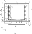
Fig. 1] Fig. 1 is a sectional view that shows an example of a detecting apparatus. - [
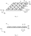
Fig. 2] Fig. 2 is a perspective view that shows an example of an electron detector. - [
Fig. 3] Fig. 3 is a sectional view that shows the example of the electron detector. - [
Fig. 4] Fig. 4 is a perspective view that shows an example of a radiation detector. - [
Fig. 5] Fig. 5 is a diagram that shows an example of Compton scattering that occurs in the detecting apparatus. - [
Fig. 6] Fig. 6 is a diagram that shows a state where an electron reaches the electron detector. - [
Fig. 7] Fig. 7 is a timing chart that shows an example of an analog signal generated by the radiation detector and an analog signal generated by the electron detector. - [
Fig. 8] Fig. 8 is a block diagram that shows an example of a circuit for generating data. - [
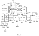
Fig. 9] Fig. 9 is a block diagram that shows an example of a second read circuit and a logic circuit. - [
Fig. 10] Fig. 10 is a block diagram that shows an example of an anode read circuit. - [
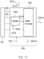
Fig. 11] Fig. 11 is a block diagram that shows an example of a first read circuit. - [
Fig. 12] Fig. 12 is a timing chart that shows an example of signal processing. - [
Fig. 13] Fig. 13 is a timing chart that shows an example of first final data and second final data transmitted to a computer. - [
Fig. 14] Fig. 14 is a timing chart that shows an example of signal processing. - [
Fig. 15] Fig. 15 is a timing chart that shows an example of signal processing in a first modification. - [
Fig. 16] Fig. 16 is a block diagram that shows a second read circuit and a logic circuit in a second modification. - [
Fig. 17] Fig. 17 is a timing chart that shows signal processing in the second modification. - [
Fig. 18] Fig. 18 is a perspective view that shows an electron detector in a third modification. - [
Fig. 19] Fig. 19 is a block diagram that shows an example of a second read circuit and a logic circuit in the third modification. - [
Fig. 20] Fig. 20 is a block diagram that shows a first read circuit, a second read circuit, and a logic circuit in a fourth modification. - [
Fig. 21] Fig. 21 is a timing chart that shows signal processing in the fourth modification. - [
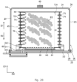
Fig. 22] Fig. 22 is a sectional view that shows an example of a detecting apparatus. - [
Fig. 23] Fig. 23 is a diagram that shows an example of absorption of a neutron that occurs in the detecting apparatus. - [
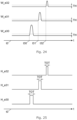
Fig. 24] Fig. 24 is a timing chart that shows an example of analog signals generated by the electron detector. - [
Fig. 25] Fig. 25 is a timing chart that shows an example of hit signals. - [
Fig. 26] Fig. 26 is a block diagram that shows an example of a circuit for generating data. - [
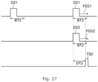
Fig. 27] Fig. 27 is a timing chart that shows an example of signal processing. - [
Fig. 28] Fig. 28 is a diagram that shows the configuration of an apparatus for measuring a maximum travel time. - [
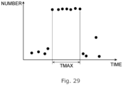
Fig. 29] Fig. 29 is a graph that shows the number of electrons detected by the apparatus ofFig. 28 . - [
Fig. 30] Fig. 30 is a timing chart that shows analog signals in a sixth modification. - [
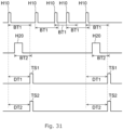
Fig. 31] Fig. 31 is a timing chart that shows signal processing in a seventh modification. - [
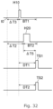
Fig. 32] Fig. 32 is a timing chart that shows signal processing in the seventh modification. - Embodiments described below are examples of the embodiment of the present disclosure, and the present disclosure should not be interpreted limitedly to these embodiments. In the specification, the terms "substrate", "base", "sheet", "film", and the like are not distinguished from each other by the difference in name. For example, "substrate" and "base" are concepts that can include components called sheets or films. Furthermore, terms "parallel", "orthogonal", and the like, values of length and angle, and the like that determine shapes, geometrical conditions and the degrees of them, used in the specification, are not limited to strict meanings and are interpreted so as to include the range of degrees to which similar functions can be expected.
- In the attached drawings to be referenced in the specification, the same or similar reference signs denote the same portions or portions having similar functions, and the repeated description can be omitted. The scale ratio of the drawings can be different from the actual ratio for the sake of convenience of illustration, and a portion of components can be omitted from the drawings.
- In the specification, when a plurality of upper limit candidates and a plurality of lower limit candidates are listed for a parameter, the numeric range of the parameter may be a combination of a selected one upper limit candidate and a selected one lower limit candidate. For example, the sentence "Parameter B, for example, may be larger than or equal to A1, may be larger than or equal to A2, or may be larger than or equal to A3. Parameter B, for example, may be smaller than or equal to A4, may be smaller than or equal to A5, or may be smaller than or equal to A6." will be discussed. In this case, the numeric range of parameter B may be larger than or equal to A1 and smaller than or equal to A4, may be larger than or equal to A1 and smaller than or equal to A5, may be larger than or equal to A1 and smaller than or equal to A6, may be larger than or equal to A2 and smaller than or equal to A4, may be larger than or equal to A2 and smaller than or equal to A5, may be larger than or equal to A2 and smaller than or equal to A6, may be larger than or equal to A3 and smaller than or equal to A4, may be larger than or equal to A3 and smaller than or equal to A5, or may be larger than or equal to A3 and smaller than or equal to A6.
- Hereinafter, the configuration of the detecting
apparatus 10 according to the embodiment of the present disclosure will be described in detail with reference to the attached drawings. First, an overview of the detectingapparatus 10 will be described.Fig. 1 is a sectional view that shows an example of the detectingapparatus 10. - The detecting
apparatus 10 includes acontainer 20, anelectron detector 30 and adrift electrode 40 located inside thecontainer 20, and aradiation detector 50. Thecontainer 20 is, for example, a chamber. At least inert gas, such as argon and xenon, is contained in thecontainer 20. In addition to the inert gas, quenching gas with quenching properties, such as carbon dioxide and methane, may be contained in thecontainer 20. - The
container 20 includes afirst part 21, asecond part 22 facing thefirst part 21 in a first direction D1, and aside part 23 extending from thefirst part 21 to thesecond part 22. The detectingapparatus 10 can be used to detect radiation that enters thecontainer 20 through thefirst part 21. As shown inFig. 1 , thecontainer 20 may have a cylindrical shape. In other words, theside part 23 may have a circular cross-section. Although not shown the drawing, thecontainer 20 may have a shape other than the cylindrical shape, such as a cubic shape or a rectangular parallelepiped shape. Thefirst part 21 may be curved to convex outward from thecontainer 20. Thecontainer 20 may have acorner 24 located between thefirst part 21 and theside part 23. Thefirst part 21 may spread out flat. Thecorner 24 may include a surface spreading out in a direction different from thefirst part 21 or theside part 23. - An object that emits radiation is located outside the
container 20. Thefirst part 21 may include a surface closest to the object of the surfaces of thecontainer 20. - The material of the
container 20 preferably allows radiation to pass easily. This can suppress the absorption or scattering of radiation by thecontainer 20 when the radiation passes through thecontainer 20. Thecontainer 20 may include, for example, plastic or metal. The plastic may be fiber reinforced plastic. When metal is used, thecontainer 20 may be made of a single metal element or may be made of an alloy. Examples of the metal include aluminum and aluminum alloys. To reduce the weight of thecontainer 20, metals with a specific gravity of less than four may be used. - When the
container 20 includes plastic, the thickness of thecontainer 20 is, for example, larger than or equal to 1 mm, may be larger than or equal to 5 mm, or may be larger than or equal to 10 mm. The thickness of thecontainer 20 is, for example, smaller than or equal to 30 mm, may be smaller than or equal to 25 mm, or may be smaller than or equal to 20 mm. - When the
container 20 includes metal, the thickness of thecontainer 20 is, for example, larger than or equal to 2 mm, may be larger than or equal to 3 mm, or may be larger than or equal to 5 mm. The thickness of thecontainer 20 is, for example, smaller than or equal to 20 mm, may be smaller than or equal to 15 mm, or may be smaller than or equal to 10 mm. - The
drift electrode 40, theelectron detector 30, and theradiation detector 50 are arranged in this order from thefirst part 21 toward thesecond part 22. In other words, thedrift electrode 40 is located closer to thefirst part 21 than theelectron detector 30. Theradiation detector 50 is located closer to thesecond part 22 than theelectron detector 30. The phrase "component element A is located closer to thefirst part 21 than component element B" means that component element A is located on the side of component element B, indicated by the arrow S1 inFig. 1 . The arrow S1 indicates a direction from thesecond part 22 toward thefirst part 21. The distance from component element A to thefirst part 21 may be longer or shorter than the distance from component element B to component element A. - The
drift electrode 40 may be more proximate to thefirst part 21 than to thesecond part 22. Theelectron detector 30 and theradiation detector 50 may be more proximate to thesecond part 22 than to thefirst part 21. - The
radiation detector 50 may be located outside thecontainer 20. For example, theradiation detector 50 may be located outside thesecond part 22. Theradiation detector 50 may face thedrift electrode 40 across thesecond part 22. - Although not shown in the drawing, the
radiation detector 50 may be located inside thecontainer 20. For example, theradiation detector 50 may be located between thesecond part 22 and theelectron detector 30. - The
electron detector 30, thedrift electrode 40, and theradiation detector 50 will be described in detail. - When radiation enters the inside of the
container 20 and collides with gas, Compton scattering may occur. When Compton scattering occurs, a recoil electron is produced. In addition, ionized electrons are produced along the track of the recoil electron. Theelectron detector 30 detects the ionized electrons. The track and energy of the recoil electron can be calculated by detecting the ionized electrons. -
Fig. 2 is a perspective view that shows an example of theelectron detector 30. Theelectron detector 30 includes a plurality of electrodes. Electrons produced through Compton scattering reach some electrodes of the plurality of electrodes. Some electrodes generate analog signals as a result of arrival of the electrons. Information about the positions of arrival of the electrons on theelectron detector 30 can be obtained by identifying some electrodes that have generated the analog signals. Information about the energy of the electrons that have reached theelectron detector 30 can be obtained based on the intensities of the analog signals. The intensities of the analog signals are calculated based on the voltages, amplitudes, and the like of the analog signals. For example, the voltages or amplitudes of the analog signals may be used as the intensities of the analog signals. - The plurality of electrodes of the
electron detector 30 may include a plurality ofanode electrodes 31, a plurality ofcathode electrodes 32, and abase 35. Thebase 35 includes afirst face 351 and asecond face 352 that spread out in a direction intersecting the first direction D1. Thefirst face 351 faces thedrift electrode 40. Thesecond face 352 is located on the opposite side from thefirst face 351. - The plurality of
cathode electrodes 32 may be located on thefirst face 351. The plurality ofcathode electrodes 32 may be arranged in a second direction D2 orthogonal to the first direction D1. Eachcathode electrode 32 may extend in a third direction D3 orthogonal to the first direction D1 and the second direction D2. - The plurality of
anode electrodes 31 may be located on thesecond face 352 and may include a plurality ofline parts 311 arranged in the third direction D3. Eachline part 311 may extend in the second direction D2.Fig. 3 is a sectional view that shows an example of theelectron detector 30. A plurality of throughparts 312 arranged in the second direction D2 and extending through the base 35 may be connected to eachline part 311. The surfaces of the throughparts 312 may be located atopenings 33 formed in thecathode electrodes 32. - Electrons produced by Compton scattering reach some of the plurality of
anode electrodes 31 and some of the plurality ofcathode electrodes 32. Some of theanode electrodes 31 generate anode analog signals as a result of arrival of the electrons. Information about the positions, in the third direction D3, of the electrons that have reached theelectron detector 30 can be obtained by identifying some of theanode electrodes 31 that have generated the anode analog signals. Some of thecathode electrodes 32 generate cathode analog signals as a result of arrival of the electrons. Information about the positions, in the second direction D2, of the electrons that have reached theelectron detector 30 can be obtained by identifying some of thecathode electrodes 32 that have generated the cathode analog signals. In this way, theelectron detector 30 shown inFigs. 2 and 3 can efficiently provide information about the positions, in the second direction D2, and the positions, in the third direction D3, of electrons that have reached theelectron detector 30. - The
electron detector 30 may be provided with a second read circuit 130 (described later) for processing analog signals. Thesecond read circuit 130 may be provided on a member different from theelectron detector 30. In this case, theelectron detector 30 may be provided with a cable, a hermetic connector, and a wiring board to carry analog signals to thesecond read circuit 130. - The
drift electrode 40 is disposed so as to face theelectron detector 30. For example, thedrift electrode 40 faces theelectron detector 30 in the first direction D1. In this case, thedrift electrode 40 includes a surface that spreads out in a direction orthogonal to the first direction D1. An electric field heading from theelectron detector 30 toward thedrift electrode 40 is generated between theelectron detector 30 and thedrift electrode 40. Ionized electrons accompanying a recoil electron produced by Compton scattering are attracted toward theelectron detector 30 by the electric field. - The
radiation detector 50 detects scattered radiation. In the present embodiment, the radiation scattered between theelectron detector 30 and thedrift electrode 40 passes through theelectron detector 30 and thesecond part 22 of the container and is then detected by theradiation detector 50. Theradiation detector 50 can detect the position and energy of radiation that have reached theradiation detector 50. -
Fig. 4 is a perspective view that shows an example of theradiation detector 50. Theradiation detector 50 may include a plurality of detectingelements 51 and acircuit board 52 that supports the detectingelements 51. The plurality of detectingelements 51 may be arranged in a direction intersecting the first direction D1. For example, the plurality of detectingelements 51 may be arranged in the second direction D2 and the third direction D3 that are orthogonal to the first direction D1. - Radiation reaches some of the plurality of detecting
elements 51. Some of the detectingelements 51 generate analog signals as a result of the arrival of the radiation. Information about the positions of arrival of the radiation on theradiation detector 50 can be obtained by identifying some of detectingelements 51 that have generated the analog signals. Information about the energy of the radiation that has reached theradiation detector 50 can be obtained based on the intensities of the analog signals. The intensities of the analog signals are calculated based on the voltages, amplitudes, and the like of the analog signals. - The configuration of the detecting
element 51 is optional as long as the detectingelement 51 can detect radiation. - For example, the detecting
element 51 may include a scintillator that is excited by scattered radiation to emit fluorescence, and a photodetector that detects the fluorescence. The photodetector may include, for example, an avalanche photodiode. - The detecting
element 51 may include a semiconductor detecting element that detects the scattered radiation. The semiconductor detecting element may, for example, include a semiconductor containing cadmium zinc telluride. - The
radiation detector 50 may include a first detectingelement 51 capable of detecting radiation with energy within a first range, and a second detectingelement 51 capable of detecting radiation with energy within a second range different from the first range. Thus, the range of energy of radiation that can be detected by theradiation detector 50 can be expanded. - Radiation detected by detecting
element 51 is processed as an electrical signal by thecircuit board 52. Thecircuit board 52 may include circuits, wires, and the like, for processing electrical signals. The electrical signals may be transmitted to the outside of thecontainer 20 through, for example, a cable, a hermetic connector, or a wiring board, connected to thecircuit board 52. - The other component elements of the detecting
apparatus 10 will be described. - As shown in
Fig. 1 , the detectingapparatus 10 may include anauxiliary drift electrode 70 located between theelectron detector 30 and thedrift electrode 40. Theauxiliary drift electrode 70 is provided to increase the uniformity of distribution of the electric field between theelectron detector 30 and thedrift electrode 40. - The
auxiliary drift electrode 70 may include a plurality ofring electrodes 72. The plurality ofring electrodes 72 is arranged in a direction in which theelectron detector 30 and thedrift electrode 40 face each other. Thering electrode 72 includes a ringfirst face 73 facing thedrift electrode 40 and a ringsecond face 74 located on the opposite side from the ringfirst face 73. - The
ring electrode 72 may include anopening 721. Theopening 721 overlaps theelectron detector 30 in the facing direction. Thering electrode 72 does not need to overlap theelectron detector 30 in the facing direction. Thering electrode 72 may overlap thedrift electrode 40 in the facing direction. - The
auxiliary drift electrode 70 may include aspacer 75 disposed between tworing electrodes 72 adjacent in the facing direction. Thespacer 75 determines the distance between tworing electrodes 72 adjacent in the facing direction. The distance is determined according to the number ofring electrodes 72, the voltage between theelectron detector 30 and thedrift electrode 40, and the like. - The
drift electrode 40 may be attached to theauxiliary drift electrode 70. For example, theauxiliary drift electrode 70 may include thespacer 75 located between thedrift electrode 40 and thering electrode 72. A structure including thedrift electrode 40 and the plurality ofring electrodes 72 is also referred to asdrift cage 45. - The
auxiliary drift electrode 70 may include awire 76 that electrically connects tworing electrodes 72 adjacent in the facing direction. Theauxiliary drift electrode 70 may include awire 76 that electrically connects thedrift electrode 40 and thering electrode 72 adjacent in the facing direction. Theauxiliary drift electrode 70 may include aresistor 77 inserted in the path of thewire 76. The voltage between the tworing electrodes 72 can be adjusted by electrically connecting the twoadjacent ring electrodes 72. Thus, the potentials of thering electrodes 72 arranged in the facing direction can be changed in a stepwise manner. For example, it is assumed that the potential of thedrift electrode 40 is - 4000 V, the potential of theelectron detector 30 is 0 V, and the 20ring electrodes 72 are disposed between thedrift electrode 40 and theelectron detector 30. In this case, the potentials of the plurality ofring electrodes 72 arranged from thedrift electrode 40 toward theelectron detector 30 can be changed in a stepwise manner like -3800 V, -3600 V, -3400 V, ... Thus, it is possible to increase the uniformity of electric field formed in the space between thedrift electrode 40 and theelectron detector 30. - As shown in
Fig. 1 , theauxiliary drift electrode 70 may be supported by arelay board 90. Therelay board 90 may support theelectron detector 30. For example, therelay board 90 may include afirst board 91 that supports theelectron detector 30 and asecond board 92 that supports theauxiliary drift electrode 70. Thesecond board 92 may be located between thefirst board 91 and theauxiliary drift electrode 70. - As shown in
Fig. 1 , the detectingapparatus 10 may include anelectronic amplifier 60 located between theelectron detector 30 and thedrift electrode 40. Theelectronic amplifier 60 is, for example, disposed so as to face theelectron detector 30 and thedrift electrode 40 in the first direction D1. - The
electronic amplifier 60 is configured to cause electron avalanche amplification. Theelectronic amplifier 60 includes an electrode having a higher potential than the potential of thedrift electrode 40. Theelectronic amplifier 60 may include a plurality of through-holes 61 that extend through theelectronic amplifier 60. Theelectronic amplifier 60 may be configured to generate electric fields heading toward thedrift electrode 40 in the through-holes 61. - Next, Compton scattering that occurs in the detecting
apparatus 10 will be described.Fig. 5 is a diagram that shows an example of Compton scattering. The reference sign R1 represents radiation that passes through thefirst part 21 of thecontainer 20 and enters thecontainer 20. The radiation R1 is, for example, charged particle radiation (such as alpha radiation and beta radiation), uncharged particle radiation (such as neutrinos and neutron radiation), electromagnetic waves (such as gamma radiation and X-radiation), or non-ionizing radiation (such as ultraviolet light). The radiation R1 passes through thedrift electrode 40 and then reaches the space between theelectron detector 30 and thedrift electrode 40. - When the radiation R1 collides with gas, Compton scattering may occur. The reference sign P represents the position where scattering has occurred. The position P is also referred to as scattering point. The reference sign R2 represents scattered radiation. The radiation R2 passes through the
electron detector 30 and then reaches theradiation detector 50. When theradiation detector 50 is located outside thecontainer 20, the radiation R2 also passes through thesecond part 22 of thecontainer 20. The radiation R2 is detected by some of the detectingelements 51 among the plurality of detectingelements 51. For example, the radiation R2 is detected by one detectingelement 51. Thus, the position of arrival and energy of the radiation R2 can be calculated. - When Compton scattering occurs, a recoil electron is produced. The reference sign R3 indicates an electron cloud formed in the track of the recoil electron. The reference sign e1 represents an electron located at the starting point of the electron cloud R3. The electron e1 may be located at the scattering point P. The reference sign e2 represents an electron located at the end point of the electron cloud R3.
- Each electron of the electron cloud R3 travels toward the
electron detector 30 due to an electric field E1. Such travel is also referred to as drift. Each electron of the electron cloud R3 that has reached theelectron detector 30 is detected by theanode electrode 31 and thecathode electrode 32 of theelectron detector 30. Thus, the position and energy of each electron of the electron cloud R3 can be calculated. In addition, the track and energy of the recoil electron and the scattering point P can be calculated. - The radiation R2 travels from the scattering point P to the
radiation detector 50 substantially at the velocity of light. The recoil electron also travels from the position of the electron e1 to the position of the electron e2 substantially at the velocity of light. On the other hand, the velocity V at which the electron cloud R3 travels toward theelectron detector 30 is slower than the velocity of light. Therefore, each electron of the electron cloud R3 reaches theelectron detector 30 after the radiation R2 reaches theradiation detector 50. The time taken for each electron of the electron cloud R3 to reach theelectron detector 30 varies depending on the distance from the electron to theelectron detector 30. In the example shown inFig. 6 , the distance from the electron e2 to theelectron detector 30 is shorter than the distance from the electron e1 to theelectron detector 30. Therefore, the electron e2 reaches theelectron detector 30 earlier than the electron e1. - In
Fig. 6 , the reference signs t0, t1, and t2 enclosed in rectangular frames respectively represent the time when the electron of the radiation R2 and the electrons of the electron cloud R3 appear at the positions represented by the reference signs or the time when the electrons reach the positions. When a time taken for the radiation R2 and the recoil electron to travel is ignored, the time at which the electron e1 is produced, the time at which the electron e2 is produced, and the time at which the radiation R2 reaches theradiation detector 50 all are t0. The electron e1 reaches theelectron detector 30 at time t1 after time t0. The electron e2 reaches theelectron detector 30 at time t2. Time t2 is later than time t0, and time t1 is later than time t2. - When the
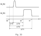
radiation detector 50 detects the radiation R2, theradiation detector 50 generates an analog signal. When theelectron detector 30 detects an electron, theelectron detector 30 generates an analog signal.Fig. 7 is a timing chart that shows an example of an analog signal W_R2 generated by theradiation detector 50 and an analog signal W_R3 generated by the electron detector. The analog signal of theradiation detector 50 is generated at time t0. A time ΔT2 is a difference between time t0 and time t2. The time ΔT2 is equivalent to a time taken for the electron e2 to travel from the end point of the electron cloud R3 to theelectron detector 30. A time ΔT1 is a difference between time t0 and time t1. The time ΔT1 is equivalent to a time taken for the electron e1 to travel from the start point of the electron cloud R3 to theelectron detector 30. - As the distance from the electron cloud R3 to the
electron detector 30 extends, electrons take longer time to travel to theelectron detector 30. A time taken for travel is longest when an electron is generated at thedrift electrode 40. The time taken for the electron to travel from thedrift electrode 40 to theelectron detector 30 is also referred to as maximum travel time TMAX. The maximum travel time TMAX is determined based on the gap (also known as drift length) between thedrift electrode 40 and theelectron detector 30 and the drift velocity V of the electron. The drift velocity V is determined based on the strength of the electric field, the type of gas and the pressure of gas in thecontainer 20, and the like. For example, in thefollowing condition 1 and condition 2, the maximum travel time TMAX is 10.24 µs. -
- Drift length: 40 cm, Electric field strength: 400 V/cm,
- Type of gas: mixed gas including argon and ethane, and Pressure of gas: 1 atm
-
- Drift length: 60 cm, Electric field strength: 600 V/cm,
- Type of gas: carbon tetrafluoride, and Pressure of gas: 3 atm
- The maximum travel time TMAX is, for example, longer than or equal to 3 µs, may be longer than or equal to 5 µs, or may be longer than or equal to 7 µs. The maximum travel time TMAX is, for example, shorter than or equal to 30 µs, may be shorter than or equal to 20 µs, or may be shorter than or equal to 15 µs.
- The maximum travel time TMAX may be measured by using an apparatus including the
electron detector 30 and thedrift electrode 40.Fig. 28 is a diagram that shows the configuration of an apparatus for measuring a maximum travel time TMAX. The apparatus includes acontainer 20, anelectron detector 30 and adrift electrode 40 located inside thecontainer 20, and aradiation source 80 located on the outer surface of thefirst part 21 of thecontainer 20. Theelectron detector 30 and thedrift electrode 40 face each other in the first direction D1 with a gap H. Theradiation source 80 is a radiation generating source. Theradiation source 80 is, for example, a radiation standard gamma-ray source (nuclide: Ba-1133, code number; BA402) of Public interest incorporated association Japan Radioisotope Association. When Compton scattering occurs inside thecontainer 20 due to radiation from theradiation source 80, a recoil electron is produced to form an electron cloud R3. -
Fig. 29 is a graph that shows the number of electrons detected by theelectron detector 30 of the apparatus ofFig. 28 . The abscissa axis of the graph ofFig. 29 represents time. The ordinate axis of the graph ofFig. 29 represents the number of electrons. A plurality of points of the graph ofFig. 29 each indicates the number of electrons detected at a predetermined sampling frequency. The sampling frequency is, for example, lower than or equal to 50 MHz. The sampling frequency may be higher than or equal to 10 MHz and lower than or equal to 20 MHz. - As shown in
Fig. 29 , the graph includes a period during which the number of electrons is large and the number is substantially constant. This period corresponds to the maximum travel time TMAX. The maximum travel time TMAX is calculated by identifying the period during which the number of electrons is large and the number is substantially constant. The drift velocity V of electrons is calculated by H / TMAX. - Next, a circuit for generating data by digitizing an analog signal of the
radiation detector 50 and an analog signal of theelectron detector 30 will be described.Fig. 8 is a block diagram that shows an example of the circuit. - The detecting
apparatus 10 includes at least afirst read circuit 150 and asecond read circuit 130. Thefirst read circuit 150 and thesecond read circuit 130 can communicate with acomputer 110. Thecomputer 110 receives digital data transmitted from thefirst read circuit 150 and thesecond read circuit 130 and processes the digital data. For example, thecomputer 110 calculates the direction of incidence of radiation into thecontainer 20 based on first final data and second final data (described later). When the size of the detectingapparatus 10 can be ignored as compared to the distance from the radiation source that emits radiation to the detectingapparatus 10 as in the case of a celestial body, one direction of incidence is determined for one radiation source. In this case, the positional relationship between the direction of incidence of the radiation and the corresponding radiation source is imaged. On the other hand, when the size of the detectingapparatus 10 cannot be ignored as compared to the distance from the radiation source that emits radiation to the detectingapparatus 10 like SPECT/PET or BNCT, a plurality of scattering points is detected for one radiation source, and the direction of incidence is determined from the scattering points. In this case, the position at which the direction of incidence identified by each scattering point converges is identified as the position of the radiation source and imaged. In this way, the combination of the detectingapparatus 10 with thecomputer 110 can function as a radiation identification apparatus that calculates the direction of incidence of radiation or images the position or the like of a radiation source for radiation. Thecomputer 110 may image an electron cloud or the like that occurs inside thecontainer 20. In this case, the combination of the detectingapparatus 10 with thecomputer 110 can function as an electronic imaging apparatus that images electrons. Thecomputer 110 may be a general-purpose personal computer or may be a calculation processing module suitable for the detectingapparatus 10. - SPECT is a single photon emission computerized tomography (single photon emission CT). BNCT is a Boron neutron capture therapy. PET is a positron emission tomography.
- The
first read circuit 150 digitizes an analog signal generated by theradiation detector 50 to generate first data D10. The first data D10 is stored in a first buffer (described later). Thefirst read circuit 150 transmits first final data FD10 to thecomputer 110 in response to input of a first trigger signal TS1. The first final data FD10 includes the first data D10 stored in the first buffer. - The
second read circuit 130 digitizes an analog signal generated by theelectron detector 30 to generate second data D20. The second data D20 is stored in a second buffer (described later). Thesecond read circuit 130 transmits second final data FD20 to thecomputer 110 in response to input of a second trigger signal TS2. The second final data FD20 includes the second data D20 stored in the second buffer. - As shown in
Fig. 8 , the detectingapparatus 10 may include alogic circuit 120 connected to thesecond read circuit 130. Thelogic circuit 120, for example, generates the first trigger signal TS1 based on the second data D20 generated by thesecond read circuit 130. For example, the first trigger signal TS1 is generated in response to generation of a second hit signal (described later) of the second data D20. Thelogic circuit 120 may generate the second trigger signal TS2 based on the second data D20. For example, the second trigger signal TS2 is generated in response to generation of a second hit signal. Thelogic circuit 120 may be connected to both thefirst read circuit 150 and thesecond read circuit 130. In this case, thelogic circuit 120 may generate trigger signals such as the first trigger signal TS1 and the second trigger signal TS2 based on both the first data D10 and the second data D20. -
Fig. 9 is a block diagram that shows an example of thesecond read circuit 130 and thelogic circuit 120. Thesecond read circuit 130 may include ananode read circuit 131 and a cathode readcircuit 132. - The anode read
circuit 131 digitizes each of anode analog signals generated by the plurality ofanode electrodes 31. Digital data generated by the anode readcircuit 131 is also referred to as twenty-first data D21. The twenty-first data D21 is part of the second data D20. The twenty-first data D21 may include a twenty-first hit signal H21. The "hit signal" is a signal generated by binarizing an analog signal. When the intensity of an analog signal exceeds a threshold, the hit signal indicates a High state. When the intensity of an analog signal is less than or equal to the threshold, the hit signal indicates a Low state. The twenty-first hit signal H21 is a signal generated by binarizing an anode analog signal. The anode readcircuit 131 may transmit the twenty-first hit signal H21 to thelogic circuit 120. - As shown in
Fig. 9 , thesecond read circuit 130 may include a plurality of the anode readcircuits 131. The number of anode readcircuits 131 is determined according to the number ofanode electrodes 31 of theelectron detector 30. When, for example, the number ofanode electrodes 31 is 256 and the number of analog signals that can be processed by the singleanode read circuit 131 is 128, thesecond read circuit 130 includes two anode readcircuits 131. - The anode read
circuit 131 may transmit twenty-first final data FD21 to thecomputer 110 in response to input of the second trigger signal TS2. The twenty-first final data FD21 includes the twenty-first data D21. The twenty-first final data FD21 is part of the second final data FD20. - The cathode read
circuit 132 digitizes each of the cathode analog signals generated by the plurality ofcathode electrodes 32. The digital data generated by the cathode readcircuit 132 is also referred to as twenty-second data D22. The twenty-second data D22 is part of the second data D20. The twenty-second data D22 may include a twenty-second hit signal H22. The twenty-second hit signal H22 is a signal generated by binarizing a cathode analog signal. Thecathode electrode 32 may transmit the twenty-second hit signal H22 to thelogic circuit 120. - As shown in
Fig. 9 , thesecond read circuit 130 may include a plurality of the cathode readcircuits 132. The number of cathode readcircuits 132 is determined according to the number ofcathode electrodes 32 of theelectron detector 30. When, for example, the number ofcathode electrodes 32 is 256 and the number of analog signals that can be processed by the singlecathode read circuit 132 is 128, thesecond read circuit 130 includes two cathode readcircuits 132. - The cathode read
circuit 132 may transmit twenty-second final data FD22 to thecomputer 110 in response to input of the second trigger signal TS2. The twenty-second final data FD22 includes the twenty-second data D22. The twenty-second final data FD22 is part of the second final data FD20. - The anode read
circuit 131 will be described in detail.Fig. 10 is a block diagram that shows an example of the configuration of the anode readcircuit 131. - The anode read
circuit 131 may include a plurality ofamplifiers 1361. Eachamplifier 1361 amplifies a corresponding one anode analog signal AS. The anode readcircuit 131 may include a plurality ofcomparators 1362. Eachcomparator 1362 may binarize the anode analog signal AS amplified by a corresponding one of theamplifiers 1361 to generate a twenty-first hit signal h21. The anode readcircuit 131 may include anamplifier 1363. Theamplifier 1363 adds the plurality of anode analog signals AS amplified by the plurality ofamplifiers 1361. The intensity of analog signal output from theamplifier 1363 indicates the intensity of electrons detected by theanode electrodes 31. For example, the waveform of the analog signal output from theamplifier 1363 shows the waveform of electrons detected by theanode electrodes 31. The plurality ofamplifiers 1361, the plurality ofcomparators 1362, and theamplifier 1363 may be made up of a firstintegrated circuit 136. The firstintegrated circuit 136 is, for example, an ASIC. - The anode read
circuit 131 may include anAD converter 137. TheAD converter 137 digitizes the analog signal output from theamplifier 1363. The data digitized by theAD converter 137 is also referred to as twenty-first intensity data W21. The twenty-first intensity data W21 is part of the twenty-first data D21. TheAD converter 137 may be a flash AD converter. In this case, an analog signal is digitized at high speed. The sampling rate of theAD converter 137 is, for example, higher than or equal to 1 MHz, may be higher than or equal to 5 MHz, or may be higher than or equal to 10 MHz. The sampling rate of theAD converter 137 is, for example, lower than or equal to 50 MHz, may be lower than or equal to 30 MHz, or may be lower than or equal to 20 MHz. The amount of data generated by theAD converter 137 can be reduced by setting a low sampling rate. Thus, the load on thecomputer 110 can be reduced. - The anode read
circuit 131 may include a twenty-first buffer 1381 and a twenty-second buffer 1382. Buffers included in thesecond read circuit 130, such as the twenty-first buffer 1381 and the twenty-second buffer 1382, are also referred to as second buffers. - The twenty-
first buffer 1381 and the twenty-second buffer 1382 are, for example, ring buffers. The twenty-first buffer 1381 and the twenty-second buffer 1382 each store the twenty-first data D21 in itself during a second storage period. The twenty-first buffer 1381 may temporarily hold the twenty-first hit signals h21. The twenty-first buffer 1381 may temporarily hold a twenty-first hit signal H21 obtained by processing the plurality of twenty-first hit signals h21 by using an OR circuit. The twenty-first hit signal H21 indicates a High state when at least one of the plurality of anode analog signals input to the anode readcircuit 131 is in a High state. The twenty-second buffer 1382 may temporarily hold the twenty-first intensity data W21. The second storage period may be shorter than or equal to the maximum travel time TMAX. - The anode read
circuit 131 may output the twenty-first hit signal H21 to thelogic circuit 120. The anode readcircuit 131 may output, to thelogic circuit 120, the twenty-first hit signal H21 before being stored in the twenty-first buffer 1381. - When the second trigger signal TS2 is input to the anode read
circuit 131, the twenty-first data D21 stored in the twenty-first buffer 1381 and the twenty-second buffer 1382 at that time is output from the twenty-first buffer 1381 and the twenty-second buffer 1382. The anode readcircuit 131 may include a seconddata processing unit 1383 that processes the output twenty-first data D21. The seconddata processing unit 1383 generates twenty-first final data FD21 to be transmitted to thecomputer 110. - The twenty-first final data at least partially includes information of the twenty-first data D21. For example, the twenty-first final data FD21 may include information of the twenty-first hit signal H21. For example, the twenty-first final data FD21 may include the twenty-first intensity data W21. The format of the information of the twenty-first data D21 included in the twenty-first final data FD21 may be the same as or different from the format of the twenty-first data D21.
- The twenty-first final data FD21 may include information about the time at which the twenty-first data D21 is stored in the twenty-
first buffer 1381 and the twenty-second buffer 1382. The twenty-first final data FD21 may include information about the positions of theanode electrodes 31 that have detected electrons. In other words, the twenty-first final data FD21 may include information about the positions of arrival of electrons on theelectron detector 30. - The twenty-
first buffer 1381, the twenty-second buffer 1382, and the seconddata processing unit 1383 may be made up of a secondintegrated circuit 138. The secondintegrated circuit 138 is, for example, an FPGA. - The anode read
circuit 131 may output a data acquisition signal DA21 to thelogic circuit 120. The data acquisition signal DA21 is a signal that enters a High state when writing of the twenty-first buffer 1381 and the twenty-second buffer 1382 is being performed. - The configuration of the cathode read
circuit 132 may be the same as the configuration of the anode readcircuit 131. - Next, the
logic circuit 120 will be described by referring back toFig. 9 . - When the
second read circuit 130 includes a plurality of the anode readcircuits 131, thelogic circuit 120 may include an ORcircuit 121 as shown inFig. 9 . The twenty-first hit signal H21 from each of the anode readcircuits 131 is input to theOR circuit 121. The ORcircuit 121 processes the plurality of twenty-first hit signals H21 to output a twenty-third hit signal H23. The twenty-third hit signal H23 indicates a High state when at least one of the plurality of twenty-first hit signals H21 is in a High state. In other word, the twenty-third hit signal H23 indicates a High state when at least one of the plurality of anode analog signals generated by the plurality ofanode electrodes 31 exceeds a threshold. The twenty-third hit signal H23 indicates a Low state when all the plurality of twenty-first hit signals H21 are in a Low state. In other words, the twenty-third hit signal H23 indicates a Low state when all the plurality of anode analog signals generated by the plurality ofanode electrodes 31 are less than or equal to the threshold. Such the twenty-third hit signal H23 is also referred to as anode hit signal. - When the
second read circuit 130 includes a plurality of the cathode readcircuits 132, thelogic circuit 120 may include an ORcircuit 122 as shown inFig. 9 . The twenty-second hit signal H22 from each of the cathode readcircuits 132 is input to theOR circuit 121. The twenty-second hit signal H22, as in the case of the twenty-first hit signal H21, indicates a High state when at least one of the plurality of cathode analog signals input to the cathode readcircuit 132 is in a High state. The ORcircuit 122 processes the plurality of twenty-second hit signals H22 to output a twenty-fourth hit signal H24. The twenty-fourth hit signal H24 indicates a High state when at least one of the plurality of twenty-second hit signal H22 is in a High state. In other word, the twenty-fourth hit signal H24 indicates a High state when at least one of the plurality of cathode analog signals generated by the plurality ofcathode electrodes 32 exceeds a threshold. The twenty-fourth hit signal H24 indicates a Low state when all the plurality of twenty-second hit signals H22 are in a Low state. In other words, the twenty-fourth hit signal H24 indicates a Low state when all the plurality of cathode analog signals generated by the plurality ofcathode electrodes 32 are less than or equal to the threshold. Such the twenty-fourth hit signal H24 is also referred to as cathode hit signal. - When the
second read circuit 130 includes the anode readcircuit 131 and the cathode readcircuit 132, thelogic circuit 120 may include an ANDcircuit 123 as shown inFig. 9 . The twenty-third hit signal H23 and the twenty-fourth hit signal H24 are input to the ANDcircuit 123. The ANDcircuit 123 processes the twenty-third hit signal H23 and the twenty-fourth hit signal H24 to generate a second hit signal H20. The second hit signal H20 indicates a High state when at least one of the plurality of anode analog signals from theelectron detector 30 exceeds a threshold and at least one of the plurality of cathode analog signals from theelectron detector 30 exceeds a threshold. The second hit signal H20 indicates a Low state when all the plurality of anode analog signals are less than or equal to the threshold or all the plurality of cathode analog signals are less than or equal to the threshold. - As shown in
Fig. 9 , thelogic circuit 120 may include aprocessing circuit 124 to which the second hit signal H20 is input. When the second hit signal H20 is input to theprocessing circuit 124, theprocessing circuit 124 generates the first trigger signal TS1. When the second hit signal H20 is input to theprocessing circuit 124, theprocessing circuit 124 may immediately generate the first trigger signal TS1. Alternatively, after a first delay time DT1 has elapsed from when the second hit signal H20 is input to theprocessing circuit 124, theprocessing circuit 124 may generate the first trigger signal TS1. The first delay time DT1 may be shorter than or equal to the maximum travel time TMAX. - After a second delay time DT2 has elapsed from when the second hit signal H20 is input to the
processing circuit 124, theprocessing circuit 124 may generate the second trigger signal TS2. The second delay time DT2 may be shorter than or equal to the maximum travel time TMAX. This can suppress generation of the second trigger signal TS2 before an electron produced at a position far from theelectron detector 30 reaches theelectron detector 30. - Next, the
first read circuit 150 will be described in detail.Fig. 11 is a block diagram that shows an example of the configuration of thefirst read circuit 150. A plurality of analog signals ES generated by the plurality of detectingelements 51 of theradiation detector 50 are input to thefirst read circuit 150. Thefirst read circuit 150 digitizes the plurality of analog signals ES to generate first data D10. - The
first read circuit 150, as in the case of the anode readcircuit 131, may include a plurality of amplifiers that amplify the plurality of analog signals ES. Thefirst read circuit 150, as in the case of the anode readcircuit 131, may include a plurality of comparators that binarize the plurality of analog signals ES to generate a plurality of hit signals. Thefirst read circuit 150 may process the plurality of hit signals by using an OR circuit to generate a first hit signal H10. Thefirst read circuit 150 may output the first hit signal H10 to thelogic circuit 120. The first hit signal H10 is part of the first data D10. The first hit signal H10 indicates a High state when at least one of the plurality of analog signals generated by the plurality of detectingelements 51 exceeds a threshold. The first hit signal H10 indicates a Low state when all the plurality of analog signals generated by the plurality of detectingelements 51 are less than or equal to the threshold. - The
first read circuit 150, as in the case of the anode readcircuit 131, may include an AD converter. The AD converter may digitize an analog signal obtained by adding the plurality of analog signals ES. The data digitized by the AD converter may also be referred to as first intensity data. - The
first read circuit 150 may include afirst buffer 1561. Thefirst buffer 1561 is, for example, a ring buffer. Thefirst buffer 1561 stores the first data D10 in itself during a first storage period. The first storage period may be shorter than or equal to the maximum travel time TMAX. When the first trigger signal TS1 is generated after the first delay time DT1 has elapsed since the second hit signal H20 is input, the first storage period may be longer than the maximum travel time TMAX. The first storage period may be shorter than the sum of the first delay time DT1 and the maximum travel time TMAX. - When the first trigger signal TS1 is input to the
first read circuit 150, the first data D10 stored in thefirst buffer 1561 at that time is output from thefirst buffer 1561. Thefirst read circuit 150 may include a firstdata processing unit 1562 that processes the output first data D10. The firstdata processing unit 1562 generates first final data FD1 to be transmitted to thecomputer 110. - The first final data FD1 at least partially includes information of the first data D10. For example, the first final data FD10 may include information of the first hit signal H10. For example, the first final data FD10 may include the first intensity data. The format of the information of the first data D10 included in the first final data FD10 may be the same as or different from the format of the first data D10.
- The first final data FD10 may include information about the time at which the first data D10 is stored in the
first buffer 1561. The first final data FD10 may include information about the position of the detectingelement 51 that has detected radiation. In other words, the first final data FD10 may include information about the position of arrival of radiation on theradiation detector 50. - The
first buffer 1561, the firstdata processing unit 1562, and the like may be made up of anintegrated circuit 156. Theintegrated circuit 156 is, for example, an FPGA. - The
first read circuit 150 may output a data acquisition signal DA10 to thelogic circuit 120. The data acquisition signal DA10 is a signal that enters a High state when writing of thefirst buffer 1561 is being performed. - Next, the
logic circuit 120 will be described by referring back toFig. 9 . As shown inFig. 9 , a VETO signal VS may be input to theprocessing circuit 124. The VETO signal VS is a signal that enters a High state when writing of the buffer is being performed in the anode readcircuit 131, the cathode readcircuit 132, or thefirst read circuit 150. When the VETO signal VS is input to theprocessing circuit 124, theprocessing circuit 124 may stop outputting the trigger signals TS1, TS2. In other words, when the VETO signal VS enters a High state, theprocessing circuit 124 may set the trigger signals TS1, TS2 to a Low state. This can suppress input of a trigger signal to the anode readcircuit 131, the cathode readcircuit 132, and thefirst read circuit 150 while writing of the buffer is being performed. - Next, an example of the operation of the detecting
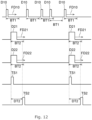
apparatus 10 will be described.Fig. 12 is a timing chart that shows an example of signal processing in the detectingapparatus 10. - When Compton scattering of radiation occurs inside the
container 20, a recoil electron and an electron cloud R3 are produced. When scattered radiation R2 is detected by theradiation detector 50, thefirst read circuit 150 generates first data D10.Fig. 12 shows the first hit signal H10 of the first data D10. The first data D10 is stored in the first buffer during the first storage period BT1. - After the radiation R2 is detected by the
radiation detector 50, electrons of the electron cloud R3 reach theelectron detector 30. When the electrons are detected by theanode electrodes 31 and thecathode electrodes 32, twenty-first data D21 and twenty-second data D22 are generated.Fig. 12 shows the anode hit signal of the twenty-first data D21 and the cathode hit signal of the twenty-second data D22. The twenty-first data D21 and the twenty-second data D22 are stored in the second buffer during the second storage period BT2. - When both the anode hit signal and the cathode hit signal enter a High state, a second hit signal is generated. When the second hit signal is generated, a first trigger signal TS1 is generated. When the first trigger signal TS1 is input to the
first read circuit 150, thefirst read circuit 150 transmits first final data FD10 including the first data D10 to thecomputer 110. - As shown in
Fig. 12 , after the second delay time DT2 has elapsed since generation of the second hit signal, a second trigger signal TS2 is generated. When the second trigger signal TS2 is input to thesecond read circuit 130, thesecond read circuit 130 transmits second final data FD20 including the second data D20 to thecomputer 110. The second final data FD20 includes twenty-first final data FD21 including the twenty-first data D21 and twenty-second final data FD22 including the twenty-second data D22. - As for the first data D10 in the first position and the first data D10 in the fifth position from the left in
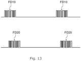
Fig. 12 , the first trigger signal TS1 is generated while the first data D10 is stored in the first buffer. Therefore, the first data D10 in the first position from the left and the first data D10 in the fifth position from the left are transmitted to thecomputer 110.Fig. 13 is a timing chart that shows an example of the first final data FD10 and the second final data FD20 to be transmitted to thecomputer 110. - On the other hand, as for the first data D10 in the second position to the first data D10 in the fourth position from the left in
Fig. 12 , the first trigger signal TS1 is not generated while the first data D10 is stored in the first buffer. This situation can occur when radiation not scattered inside thecontainer 20 reaches theradiation detector 50. This situation can also occur when radiation that has not passed through thecontainer 20 reaches theradiation detector 50. The first data D10 in the second position from the left to the first data D10 in the fourth position from the left are not transmitted to thecomputer 110 and are erased. -
Fig. 14 is a timing chart that shows another example of signal processing. In the example shown inFig. 14 , the first data D10 in the first position from the left is accompanied by generation of the twenty-first data D21 and not accompanied by generation of the twenty-second data D22. Therefore, the first trigger signal TS1 is not generated while the first data D10 is stored in the first buffer. This situation can occur when the energy of electrons of the electron cloud R3 is low. When the energy of electrons is low, it is difficult to accurately calculate the track and the like of the recoil electron. Therefore, the usefulness of the first data D10 and the second data D20 in the case where the energy of electrons is low is low. The first data D10 in the first position from the left is not transmitted to thecomputer 110 and is erased. - The
computer 110 calculates information about radiation and electrons based on the first final data FD10 and the second final data FD20. For example, thecomputer 110 may calculate the position of arrival of radiation R2, the energy of the radiation R2, the track of a recoil electron, the energy of the recoil electron, the position of the scattering point P, and the like. Thecomputer 110 may calculate the direction of incidence of radiation that has entered thecontainer 20 based on these pieces of information. Thecomputer 110 may image the position of the radiation source of the radiation that has entered thecontainer 20. - According to the present embodiment, the first data D10 regarding radiation that does not involve proper production of electrons inside the
container 20 is not transmitted to thecomputer 110 and is erased. Therefore, the amount of first data D10 transmitted to thecomputer 110 can be reduced. Thus, the load on thecomputer 110 can be reduced. For example, the load used for calculation processing, image processing, and the like of first data D10 is reduced. For example, the load used for communication of first data D10 is reduced. Thus, thecomputer 110 can preferentially process useful data. Therefore, it is possible to calculate faster the direction of incidence of radiation that has entered thecontainer 20 as compared to the existingcomputer 110. Therefore, when, for example, the detectingapparatus 10 detects radiation radiated from radioactive drugs inside a patient's body, the degree of patient exposure can be reduced. - Various changes may be applied to the above-described embodiment. Hereinafter, modifications will be described with reference to the attached drawings as needed. In the following description and the drawings used in the following description, like reference signs to the reference signs used for corresponding portions in the above-described embodiment are used for portions that can be similarly configured to those of the first embodiment, and the description thereof will not be repeated. Furthermore, if the operational effects obtained in the above-described embodiment are also apparent in the modifications, the description thereof may be omitted.
-
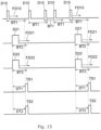
Fig. 15 is a timing chart that shows an example of signal processing in the first modification. As shown inFig. 15 , the first trigger signal TS1 and the second trigger signal TS2 may be generated simultaneously in response to the second hit signal. For example, the first delay time DT1 may be the same as the second delay time DT2. - In the example shown in
Fig. 15 as well, when the first trigger signal TS1 is generated while the first data D10 is stored in the first buffer, the first final data FD10 is transmitted to thecomputer 110. -
Fig. 16 is a block diagram that shows asecond read circuit 130 and alogic circuit 120 in the second modification. As shown inFig. 16 , the anode hit signal H23 and the cathode hit signal H24 may be input to an OR circuit 125. The OR circuit 125 processes the twenty-third hit signal H23 and the twenty-fourth hit signal H24 to generate a second hit signal H20. The second hit signal H20 indicates a High state when at least one of the plurality of anode analog signals from theelectron detector 30 exceeds a threshold or at least one of the plurality of cathode analog signals from theelectron detector 30 exceeds a threshold. The second hit signal H20 indicates a Low state when all the plurality of anode analog signals are less than or equal to the threshold and all the plurality of cathode analog signals are less than or equal to the threshold. When the second hit signal H20 is input to theprocessing circuit 124, theprocessing circuit 124 generates the first trigger signal TS1. -
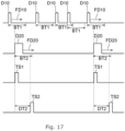
Fig. 17 is a timing chart that shows an example of signal processing in the second modification. When electrons are detected by theanode electrodes 31 or thecathode electrodes 32, second data D20 is generated.Fig. 17 shows a second hit signal of the second data D20. - When the second hit signal is generated, a first trigger signal TS1 is generated. When the first trigger signal TS1 is input to the
first read circuit 150, thefirst read circuit 150 transmits first final data FD10 including the first data D10 to thecomputer 110. - After the second delay time DT2 has elapsed since generation of the second hit signal, a second trigger signal TS2 is generated. When the second trigger signal TS2 is input to the
second read circuit 130, thesecond read circuit 130 transmits second final data FD20 including the second data D20 to thecomputer 110. - In this modification as well, the first data D10 regarding radiation that does not involve generation of electrons inside the
container 20 is not transmitted to thecomputer 110 and is erased. Therefore, the amount of first data D10 transmitted to thecomputer 110 can be reduced. Thus, the load on thecomputer 110 can be reduced. For example, the load used for calculation processing, image processing, and the like of first data D10 is reduced. -
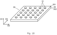
Fig. 18 is a perspective view that shows theelectron detector 30 in the third modification. As shown inFig. 18 , theelectron detector 30 includes a plurality ofanode electrodes 31 arranged in the second direction D2 and the third direction D3. Theelectron detector 30 may include a single cathode electrode facing the plurality ofanode electrodes 31. -
Fig. 19 is a block diagram that shows an example of thesecond read circuit 130 and thelogic circuit 120 in the third modification. Thesecond read circuit 130 includes anode readcircuits 131 but does not include a cathode read circuit. In this case, theOR circuit 121 may generate a second hit signal H20. The second hit signal H20 indicates a High state when at least one of the plurality of anode analog signals from theelectron detector 30 exceeds a threshold. The second hit signal H20 indicates a Low state when all the plurality of anode analog signals are less than or equal to the threshold. - An example of signal processing in the third modification is the same as an example of signal processing in the second modification shown in
Fig. 17 . In this modification as well, the first data D10 regarding radiation that does not involve generation of electrons inside thecontainer 20 is not transmitted to thecomputer 110 and is erased. Therefore, the amount of first data D10 transmitted to thecomputer 110 can be reduced. Thus, the load on thecomputer 110 can be reduced. For example, the load used for calculation processing, image processing, and the like of first data D10 is reduced. - In this modification, both the first trigger signal TS1 and the second trigger signal TS2 are generated based on both the first hit signal and the second hit signal.
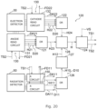
Fig. 20 is a block diagram that shows afirst read circuit 150, asecond read circuit 130, and alogic circuit 120 in the fourth modification. - As shown in
Fig. 20 , the detectingapparatus 10 may include a plurality of thefirst read circuits 150. The number offirst read circuits 150 is determined according to the number of detectingelements 51 of theradiation detector 50. For example, when the number of detectingelements 51 is 64 and the number of analog signals that can be processed by onefirst read circuit 150 is 32, the detectingapparatus 10 includes twofirst read circuits 150. - The
first read circuit 150 may transmit eleventh final data FD11 to thecomputer 110 in response to input of the first trigger signal TS1. The eleventh final data FD11 is part of the first final data FD10. The eleventh final data FD11 may include an eleventh hit signal H11. The eleventh hit signal H11 indicates a High state when at least one of the plurality of analog signals input to thefirst read circuit 150 is in a High state. - As shown in
Fig. 20 , a plurality of the eleventh hit signals H11 may be input to theOR circuit 126. The ORcircuit 126 outputs a first hit signal H10. - The
logic circuit 120 may include aprocessing circuit 127 to which the first hit signal H10 is input. Theprocessing circuit 127 outputs a retention signal H12. The retention signal H12 indicates a High state during a first retention period from when the first hit signal H10 is generated. The first retention period is a period for waiting for an electron produced at a position far from theelectron detector 30 reaches theelectron detector 30. The first retention period may be shorter than or equal to the maximum travel time TMAX. - The
logic circuit 120 may include aprocessing circuit 128 to which the twenty-third hit signal H23, the twenty-fourth hit signal H24, and the retention signal H12 are input. Theprocessing circuit 128 generates a second hit signal based on the twenty-third hit signal H23 and the twenty-fourth hit signal H24. For example, theprocessing circuit 128, as in the case of the ANDcircuit 123, may generate a second hit signal when both the anode hit signal H23 and the cathode hit signal H24 are in a High state. Alternatively, theprocessing circuit 128, as in the case of the OR circuit 125 according to the second modification, may generate a second hit signal when any one of the anode hit signal H23 and the cathode hit signal H24 is in a high state. Theprocessing circuit 128 generates a hit signal H when the retention signal H12 is in a High state at the time when the second hit signal is generated. - With the combination of the
processing circuit 127 with theprocessing circuit 128, when a second hit signal is generated within the first retention period since generation of the first hit signal H10, a hit signal H can be generated. The hit signal H is input to theprocessing circuit 124. - When the hit signal H is input to the
processing circuit 124, theprocessing circuit 124 generates a first trigger signal TS1. When the hit signal H is input to theprocessing circuit 124, theprocessing circuit 124 may immediately generate the first trigger signal TS1. Alternatively, after a first delay time DT1 has elapsed from when the hit signal H is input to theprocessing circuit 124, theprocessing circuit 124 may generate the first trigger signal TS1. After a second delay time DT2 has elapsed since the hit signal H is input to theprocessing circuit 124, theprocessing circuit 124 may generate a second trigger signal TS2. -
Fig. 21 is a timing chart that shows an example of signal processing in the fourth modification. When scattered radiation R2 is detected by theradiation detector 50, thefirst read circuit 150 generates first data D10.Fig. 21 shows the first hit signal H10 of the first data D10. The retention signal H12 indicates a High state during a first retention period KT1 since generation of the first hit signal H10. - When a second hit signal is generated during the first retention period KT1, a first trigger signal TS1 and a second trigger signal TS2 are generated. In the example shown in
Fig. 21 , as for the first data D10 in the fourth position from the left, twenty-first data D21 and twenty-second data D22 are generated to generate a second hit signal during the first retention period KT1. Therefore, the first data D10 in the fourth position from the left is transmitted to thecomputer 110. In addition, the twenty-first data D21 in the second position from the left and the twenty-second data D22 in the second position from the left, which are produced together with the first data D10 in the fourth position from the left, are also transmitted to thecomputer 110. - On the other hand, as for the twenty-first data D21 in the first position from the left and the twenty-second data D22 in the first position from the left, the corresponding first data D10 is not generated. Therefore, a second trigger signal TS2 is not generated. This situation can occur when electrons not caused by Compton scattering are detected by the
electron detector 30. The twenty-first data D21 in the first position from the left and the twenty-second data D22 in the first position from the left are not transmitted to thecomputer 110 and are erased. - According to this modification, the second data D20, such as the twenty-first data D21 and the twenty-second data D22, related to electrons not caused by Compton scattering, are not transmitted to the
computer 110 and are erased. Therefore, the amount of second data D20 transmitted to thecomputer 110 can be reduced. Thus, the load on thecomputer 110 can be reduced. For example, the load used for calculation processing, image processing, and the like of second data D20 is reduced. For example, the load used for communication of second data D20 is reduced. Thus, thecomputer 110 can preferentially process useful data. Therefore, it is possible to calculate faster the direction of incidence of radiation that has entered thecontainer 20 as compared to the existingcomputer 110. Therefore, when, for example, the detectingapparatus 10 detects radiation radiated from radioactive drugs inside a patient's body, the degree of patient exposure can be reduced. -
Fig. 22 is a sectional view that shows a detectingapparatus 10 in the fifth modification. The detectingapparatus 10 includes acontainer 20, and anelectron detector 30 and adrift electrode 40 located inside thecontainer 20. The detectingapparatus 10 does not need to include a radiation detector. At least helium-3 (3He) is contained in thecontainer 20. Helium-3 is a stable isotope of a normal helium atom (4He). An atomic nucleus of helium-3 includes two protons and one neutron. In addition to helium-3, mixed gas of argon and ethane may be contained in thecontainer 20. - The detecting
apparatus 10 is expected to detect a neutron that enters the inside of thecontainer 20 through thefirst part 21. When a neutron that have entered the side of thecontainer 20 is absorbed by helium-3, a proton and tritium (3H) are produced.Fig. 23 is a diagram that shows a state where a neutron enters the inside of thecontainer 20. The reference sign R4 represents, for example, a neutron generated by an accelerator and incoming from a point at infinity. The detectingapparatus 10 is disposed such that the face of thefirst part 21 of thecontainer 20 is orthogonal to the direction of incidence of the neutron R4. The reference sign P represents a position where the neutron is absorbed by helium-3. The position P is also referred to as absorption point. - The proton and tritium produced at the absorption point P fly in opposite directions from each other. Electron clouds made up of electrons that occur as a result of ionization of argon are formed in the tracks of a proton and tritium. The reference sign R31 represents an electron cloud formed in the track of a proton, and the reference sign R32 represents an electron cloud formed in the track of tritium. The reference sign e30 represents an electron located at the end point of the electron cloud R31, and the reference sign e40 represents an electron located at the end point of the electron cloud R32. The reference sign e31 and the reference sign e32 represent electrons in the electron cloud R31 located between the absorption point P and e30.
- In
Fig. 23 , the reference sign TL represents the sum of the length of the electron cloud R31 and the length of the electron cloud R32 in the surface direction of theelectron detector 30. The mass of a proton is 1/3 of the mass of tritium. Therefore, the length of the electron cloud R31 is three times the length of the electron cloud R32. The position of the absorption point P projected on the surface of theelectron detector 30 is calculated as a position displaced by 1/TL in the length direction from the position of the electron e40 projected on the surface of theelectron detector 30. The length direction is a direction from the position of the electron e40 projected on the surface of theelectron detector 30 toward the position of the electron e30 projected on the surface of theelectron detector 30. - Each of the plurality of electrodes of the
electron detector 30 generates an analog signal when detecting an electron.Fig. 24 is a timing chart that shows an example of analog signals W_e30, W_e31, and W_e32. The analog signal W_e30 is generated by an electrode that has detected the electron e30 in the electron cloud R31. The analog signal W_e31 is generated by an electrode that has detected the electron e31 in the electron cloud R31. The analog signal W_e32 is generated by an electrode that has detected the electron e32 in the electron cloud R31. - The distance from the electron e30 to the
electron detector 30 is shorter than the distance from the electron e31 to theelectron detector 30. The distance from the electron e31 to theelectron detector 30 is shorter than the distance from the electron e32 to theelectron detector 30. Therefore, as shown inFig. 24 , the peak of an analog signal generated by detecting an electron appears in order of the analog signal W_e30, the analog signal W_e31, and the analog signal W_e32. - In the electron cloud R31 of the proton, the peak of the analog signal increases as the position approaches the end point. Therefore, the peak of the analog signal W_e30 due to the electron e30 is larger than the peak of the analog signal W_e31 due to the electron e31. Furthermore, the peak of the analog signal W_e31 due to the electron e31 is larger than the peak of the analog signal W_e32 due to the electron e32.
- As described above, the
second read circuit 130 digitizes each of analog signals generated by the electrodes of theelectron detector 30. Thesecond read circuit 130 generates a hit signal that indicates a High state when the intensity of an analog signal exceeds a threshold. InFig. 24 , the reference sign TH represents a threshold. - As the peak of an analog signal increases, a period during which the intensity of the analog signal exceeds a threshold extends. Therefore, as the peak of the analog signal increases, a period during which a hit signal is being generated, that is, a period of a High state extends. The period of a High state in a hit signal is also referred to as TOT (time over threshold).
Fig. 25 is a timing chart that shows hit signals H_e30, H_e31, and H_e32 generated from the analog signals W_e30, W_e31, and W_e32. - In the electron cloud R31 of the proton, the peak of the analog signal increases as the position moves away from the absorption point P, with the result that the TOT extends. Therefore, based on the difference in position on the
electron detector 30 of the TOT of a hit signal, as shown inFig. 25 , it is possible to identify the electron e30 located at the end point of the electron cloud R31. - In the electron cloud R32 of the tritium, the peak of the analog signal reduces as the position moves away from the absorption point P, in contrast to the case of the electron cloud R31 of the proton. Therefore, regarding the electron cloud R32 of tritium as well, it is possible to identify the electron e40 located at the end point of the electron cloud R32 based on the difference in position on the
electron detector 30 of the TOT of the hit signal, as shown inFig. 25 . -
Fig. 26 is a block diagram that shows an example of a circuit for digitizing an analog signal of theelectron detector 30 to generate data. The detectingapparatus 10 includes at least thesecond read circuit 130. Thesecond read circuit 130 can communicate with acomputer 110. The detectingapparatus 10 may include alogic circuit 120 connected to thesecond read circuit 130. - As shown in
Fig. 5 , when theelectron detector 30 includes a plurality ofanode electrodes 31 and a plurality ofcathode electrodes 32, thesecond read circuit 130 generates a plurality of twenty-first hit signals H21 and a plurality of twenty-second hit signals H22. - The second final data FD20 transmitted from the
second read circuit 130 to thecomputer 110 may include a plurality of twenty-first hit signals H21 and a plurality of twenty-second hit signals H22. In this case, thecomputer 110 may calculate a plurality of pieces of anode TOT information and a plurality of pieces of cathode TOT information based on the plurality of twenty-first hit signals H21 and the plurality of twenty-second hit signals H22. The plurality of anode TOTs is information about TOTs of the plurality of twenty-first hit signals H21. The plurality of cathode TOTs is information about TOTs of the plurality of twenty-second hit signals H22. Thecomputer 110 may identify the electron e30 located at the end point of the electron cloud R31 and the electron e40 located at the end point of the electron cloud R32 based on the plurality of pieces of anode TOT information and the plurality of pieces of cathode TOT information. Thecomputer 110 may image the position of incidence of the neutron R4 into the detectingapparatus 10 based on the position of the electron e30 and the position of the electron e40. In this way, the combination of the detectingapparatus 10 with thecomputer 110 can function as a neutron imaging apparatus that images a neutron. - The twenty-first hit signal H21 may include information about the rise and fall of the anode analog signal. In other words, in the twenty-first hit signal H21, the rise and fall of the anode analog signal may be differentiated. Rise means the timing when the anode analog signal exceeds a threshold, and fall means the timing when the anode analog signal falls below the threshold. Similarly, the twenty-second hit signal H22 may include information about the rise and fall of the cathode analog signal. In other words, in the twenty-second hit signal H22, the rise and fall of the cathode analog signal may be differentiated. By using information on the rise and fall, the
computer 110 can further accurately calculate a plurality of pieces of anode TOT information and a plurality of pieces of cathode TOT information. - The plurality of pieces of anode TOT information and the plurality of pieces of cathode TOT information may be calculated not in the
computer 110 but in thesecond read circuit 130. In other words, thesecond read circuit 130 may calculate a plurality of pieces of anode TOT information and a plurality of pieces of cathode TOT information based on a plurality of the twenty-first hit signals H21 and a plurality of the twenty-second hit signals H22. In this case, the second final data FD20 may include a plurality of pieces of anode TOT information and a plurality of pieces of cathode TOT information. Thecomputer 110 may image the position of incidence of the neutron R4 to the detectingapparatus 10 based on the plurality of pieces of anode TOT information and the plurality of pieces of cathode TOT information. -
Fig. 27 is a timing chart that shows an example of signal processing in the detectingapparatus 10. - When the neutron R4 is absorbed by helium-3, the electron cloud R31 of the proton and the electron cloud R32 of the tritium are formed. When the electrons in the electron clouds R31, R32 are detected by the
anode electrodes 31 and thecathode electrodes 32 of theelectron detector 30, twenty-first data D21 and twenty-second data D22 are generated.Fig. 27 shows the anode hit signal of the twenty-first data D21 and the cathode hit signal of the twenty-second data D22. The twenty-first data D21 and the twenty-second data D22 are stored in the second buffer during the second storage period BT2. - When both the anode hit signal and the cathode hit signal enter a High state, a second hit signal is generated. After the second delay time DT2 has elapsed since generation of the second hit signal, a second trigger signal TS2 is generated. When the second trigger signal TS2 is input to the
second read circuit 130, thesecond read circuit 130 transmits second final data FD20 including the second data D20 to thecomputer 110. The second final data FD20 includes twenty-first final data FD21 including the twenty-first data D21 and twenty-second final data FD22 including the twenty-second data D22. - In
Fig. 27 , the twenty-first data D21 in the first position from the left is not accompanied by generation of the twenty-second data D22. Therefore, the second trigger signal TS2 is not generated while the twenty-first data D21 is stored in the second buffer. The twenty-first data D21 in the first position from the left is not transmitted to thecomputer 110 and is erased. This situation can occur when the energy of electrons of the electron clouds R31, R32 is low. - In this modification as well, the second data regarding a neutron that does not involve proper production of electrons inside the
container 20 is not transmitted to thecomputer 110 and is erased. Therefore, the amount of second data transmitted tocomputer 110 can be reduced. Thus, the load on thecomputer 110 can be reduced. For example, the load used for calculation processing, image processing, and the like of second data is reduced. For example, the load used for communication of second data is reduced. Thus, thecomputer 110 can preferentially process useful data. Therefore, for example, it is possible to calculate faster the position of incidence of a neutron that has entered thecontainer 20 as compared to the existingcomputer 110. - In the above embodiment, as shown in
Fig. 7 , a calculation method on the assumption that the analog signal of theradiation detector 50 is generated at time t0 has been described. In this modification, an example in which an analog signal of theradiation detector 50 is generated after a lapse of a time ΔT3 from time t0, as shown inFig. 30 , will be described. The time ΔT3 may be a difference between the time at which the first hit signal H10 rises and time t0. The first hit signal H10 is obtained by digitizing the analog signal of theradiation detector 50. The time ΔT3 is also referred to as a detection delay time. - ΔT4 in
Fig. 30 represents a time from when radiation is detected by theradiation detector 50 to when electrons are detected by theelectron detector 30. The time ΔT4 may be a difference between the time at which the first hit signal H10 rises and the time at which the second hit signal H20 rises. - The time ΔT2 is calculated by adding the time ΔT3 to the time ΔT4. The time ΔT2 is equivalent to a time taken for the electron e2 to travel from the end point of the electron cloud R3 to the
electron detector 30. The time ΔT1 is also calculated in consideration of the time ΔT3. The time ΔT1 is equivalent to a time taken for the electron e1 to travel from the start point of the electron cloud R3 to theelectron detector 30. Thecomputer 110 may identify the position of the electron cloud in consideration of the time ΔT2 and the time ΔT1. For example, thecomputer 110 may identify the coordinates of electrons e1 and e2 in the first direction D1 in consideration of the time ΔT2 and the time ΔT1. For example, thecomputer 110 may image the electron cloud in consideration of the time ΔT2 and the time ΔT1. - The time ΔT3 occurs depending on the
radiation detector 50. For example, the time ΔT3 in theradiation detector 50 including a semiconductor detecting element can be longer than the time ΔT3 in theradiation detector 50 including a scintillator. - The
computer 110 may acquire information about the time ΔT3 from theradiation detector 50. For example, theradiation detector 50 may transmit, to thecomputer 110, a signal digitized from information including the time ΔT3. Thecomputer 110 may calculate information about the time ΔT3 based on an analog signal of theradiation detector 50. - When the
radiation detector 50 includes a semiconductor detecting element, there can be some relationship between the time ΔT3 and the intensity of the analog signal. A semiconductor detecting element includes a cathode electrode and an anode electrode. After the radiation R2 passes through the cathode electrode, an electron is produced at a position between the cathode electrode and the anode electrode. When the energy of the radiation R2 is small, an electron is produced at a position far from the anode electrode. In this case, the travel distance of the electron to reach the anode electrode is long, so the time ΔT3 is long. In addition, since the energy of the radiation R2 is small, the intensity of the analog signal is also low. On the other hand, when the energy of the radiation R2 is large, an electron is produced at a position close to the anode electrode. In this case, the travel distance of the electron to reach the anode electrode is short, so the time ΔT3 is short. In addition, since the energy of the radiation R2 is large, the intensity of the analog signal is also high. The time ΔT3 can be calculated based on the intensity of the analog signal. - In the above embodiment, an example in which a first trigger signal TS1 is generated originally from a signal from the
electron detector 30 has been described. For example, inFigs. 12 ,14 ,17 , and21 , an example in which a first trigger signal TS1 is generated when a second hit signal is generated has been described. For example, inFig. 15 , an example in which a first trigger signal TS1 is generated after a first delay time DT1 has elapsed since generation of a second hit signal has been described. In this modification, an example in which a first trigger signal TS1 is generated originally from a signal from theradiation detector 50 will be described. -
Fig. 31 is a timing chart that shows signal processing in the seventh modification. A first trigger signal TS1 may be generated after a first delay time DT1 has elapsed since generation of a first hit signal H10 of first data. - The first delay time DT1 may be the same as the maximum travel time TMAX. The first delay time DT1 may be substantially the same as the maximum travel time TMAX. The phrase "substantially the same" means that the first delay time DT1 is 0.90 times or longer and 1.00 time or shorter of the maximum travel time TMAX. The first delay time DT1 may be 0.45 times or longer and 1.00 time or shorter of the maximum travel time TMAX.
- A first trigger signal TS1 may be generated only after a first delay time DT1 has elapsed since generation of a first hit signal H10 and when it is determined that a second hit signal H20 has been generated during the first delay time DT1. In other words, when a second hit signal H20 is not generated during the first delay time DT1, a first trigger signal TS1 does not need to be generated after the first delay time DT1 has elapsed since generation of a first hit signal H10.
- As shown in
Fig. 31 , a second trigger signal TS2 may also be generated after a first delay time DT1 has elapsed since generation of a first hit signal H10. A second trigger signal TS2 may be generated only after a first delay time DT1 has elapsed since generation of a first hit signal H10 and when it is determined that a second hit signal H20 has been generated during the first delay time DT1. In other words, when a second hit signal H20 is not generated during the first delay time DT1, a second trigger signal TS2 does not need to be generated after the first delay time DT1 has elapsed since generation of a first hit signal H10. -
Fig. 32 is a timing chart that shows an example of a calculation method for the time ΔT2. After a first trigger signal TS1 is generated, a time ΔT5 is calculated. The time ΔT5 is a difference between the time at which a second hit signal H20 rises and the time at which the first trigger signal TS1 rises. A time ΔT2 is calculated by subtracting the time ΔT5 from the sum of a time ΔT3 and the first delay time DT1. - As described in the embodiments and various modifications, the phrase "generating a hit signal" may mean "setting a hit signal to a High state". Similarly, the phrase "generating a trigger signal" may mean "setting a trigger signal to a High state". When the circuit of the detecting
apparatus 10 performs some operation upon reception of a signal in a Low state, the phrase "generating a signal for generating a hit signal" may mean "setting a hit signal to a Low state". Similarly, the phase "generating a signal for generating a trigger signal" may mean "setting a trigger signal to a Low state". - Some modifications to the above-described embodiments have been described; of course, it is also possible to apply a plurality of modifications in combination as needed to the above-described embodiments.
-
- 5 object
- 10 detecting apparatus
- 20 container
- 30 electron detector
- 31 anode electrode
- 32 cathode electrode
- 35 base
- 351 first face
- 352 second face
- 40 drift electrode
- 45 drift cage
- 50 radiation detector
- 51 detecting element
- 52 circuit board
- 60 electronic amplifier
- 70 auxiliary drift electrode
- 110 computer
- 120 logic circuit
- 130 second read circuit
- 131 anode read circuit
- 132 cathode read circuit
- 136 first integrated circuit
- 137 AD converter
- 138 second integrated circuit
- 1381 twenty-first buffer
- 1382 twenty-second buffer
- 1383 second data processing unit
- 150 first read circuit
- 156 integrated circuit
- 1561 first buffer
- 1562 first data processing unit
Claims (19)
- A detecting apparatus that detects an electron, the detecting apparatus comprising:a container containing gas;an electron detector located inside the container, the electron detector detecting an electron of an electron cloud formed inside the container to generate an analog signal;a drift electrode facing the electron detector; anda second read circuit digitizing the analog signal generated by the electron detector to generate second data, whereinthe second read circuit includes a second buffer in which the second data is stored, andthe second read circuit transmits second final data including the second data stored in the second buffer to an external computer in response to a second trigger signal.
- The detecting apparatus according to claim 1, whereinthe detecting apparatus comprises a logic circuit connected to the second read circuit,the second read circuit generates a second hit signal when an intensity of the analog signal of the electron detector exceeds a threshold, andthe logic circuit generates the second trigger signal after a second delay time has elapsed since generation of the second hit signal in the electron detector.
- The detecting apparatus according to claim 1, whereinthe detecting apparatus comprises a logic circuit connected to the second read circuit,the electron detector includes a plurality of anode electrodes and a plurality of cathode electrodes,the analog signal of the electron detector includes anode analog signals generated by the plurality of anode electrodes and cathode analog signals generated by the plurality of cathode electrodes,the second read circuit generates an anode hit signal when an intensity of the anode analog signal exceeds a threshold and generates a cathode hit signal when an intensity of the cathode analog signal exceeds a threshold, andthe logic circuit generates the second trigger signal in response to generation of both the anode hit signal and the cathode hit signal.
- The detecting apparatus according to claim 3, whereinthe detecting apparatus comprises a logic circuit connected to the second read circuit, andthe logic circuit generates the second trigger signal after a second delay time has elapsed since generation of both the anode hit signal and the cathode hit signal.
- The detecting apparatus according to claim 2 or 4, whereinthe second delay time is shorter than or equal to a maximum travel time, andthe maximum travel time is a time taken for an electron to travel from the drift electrode to the electron detector.
- The detecting apparatus according to claim 2 or 4, whereinthe second buffer of the second read circuit stores the second data during a second storage period,the second storage period is longer than or equal to the second delay time.
- The detecting apparatus according to any one of claims 1 to 4, wherein the second final data includes information about an intensity of the analog signal generated by the electron detector.
- The detecting apparatus according to claim 7, wherein the second read circuit acquires information about the intensity of the analog signal generated by the electron detector at a sampling frequency of lower than or equal to 50 MHz.
- The detecting apparatus according to claim 7, wherein the second read circuit acquires information about the intensity of the analog signal generated by the electron detector at a sampling frequency of higher than or equal to 10 MHz and lower than or equal to 20 MHz.
- The detecting apparatus according to any one of claims 1 to 4, wherein the second final data includes information about time when the second data is stored in the second buffer.
- The detecting apparatus according to any one of claims 1 to 4, wherein the second final data includes information about a position of arrival of an electron on the electron detector.
- The detecting apparatus according to any one of claims 1 to 4, whereinthe electron cloud is formed in a track of a recoil electron produced by Compton scattering, andthe detecting apparatus comprises a radiation detector detecting radiation scattered by the Compton scattering to generate an analog signal, and a first read circuit digitizing the analog signal generated by the radiation detector to generate first data and transmitting first final data including the first data to an external computer.
- The detecting apparatus according to any one of claims 1 to 4, wherein the electron cloud is formed in tracks of tritium and a proton produced by a nuclear reaction of a neutron.
- The detecting apparatus according to claim 13, whereinthe electron detector includes a plurality of anode electrodes and a plurality of cathode electrodes,the analog signal of the electron detector includes a plurality of anode analog signals generated by the plurality of anode electrodes and a plurality of cathode analog signals generated by the plurality of cathode electrodes,the second read circuit generates an anode hit signal with a differentiation between rise and fall of a signal when an intensity of the anode analog signal exceeds a threshold, and generates a cathode hit signal with a differentiation between rise and fall of a signal when an intensity of the cathode analog signal exceeds a threshold, andthe second final data includes a plurality of the anode hit signals corresponding to the plurality of anode electrodes, and a plurality of the cathode hit signals corresponding to the plurality of cathode electrodes.
- The detecting apparatus according to claim 13, whereinthe electron detector includes a plurality of anode electrodes and a plurality of cathode electrodes,the analog signal of the electron detector includes a plurality of anode analog signals generated by the plurality of anode electrodes and a plurality of cathode analog signals generated by the plurality of cathode electrodes,the second read circuit generates an anode hit signal when an intensity of the anode analog signal exceeds a threshold, and generates a cathode hit signal when an intensity of the cathode analog signal exceeds a threshold,the second final data includes a plurality of pieces of anode TOT information related to the plurality of anode electrodes and a plurality of pieces of cathode TOT information related to the plurality of cathode electrodes,each piece of the anode TOT information is information about a period in which a corresponding one of the anode hit signals is generated, andeach piece of the cathode TOT information is information about a period in which a corresponding one of the cathode hit signals is generated.
- A radiation identification apparatus comprising:the detecting apparatus according to claim 12; anda computer receiving the first final data and the second final data, transmitted from the detecting apparatus, whereinthe computer calculates a direction of incidence of radiation to the detecting apparatus based on the first final data and the second final data.
- A radiation identification apparatus comprising:the detecting apparatus according to claim 12; anda computer receiving the first final data and the second final data, transmitted from the detecting apparatus, whereinthe computer images a position of a radiation source based on the first final data and the second final data, the radiation source radiating radiation.
- A neutron imaging apparatus comprising:the detecting apparatus according to claim 14; anda computer receiving the second final data transmitted from the detecting apparatus, whereinthe computer images a position of incidence of a neutron to the detecting apparatus based on the second final data.
- A neutron imaging apparatus comprising:the detecting apparatus according to claim 15; anda computer receiving the second final data transmitted from the detecting apparatus, whereinthe computer images a position of incidence of a neutron to the detecting apparatus based on the second final data.
Applications Claiming Priority (2)
| Application Number | Priority Date | Filing Date | Title |
|---|---|---|---|
| JP2022138726 | 2022-08-31 | ||
| PCT/JP2023/032011 WO2024048761A1 (en) | 2022-08-31 | 2023-08-31 | Detection apparatus, radiation identification apparatus, and neutron imaging apparatus |
Publications (2)
| Publication Number | Publication Date |
|---|---|
| EP4582838A1 true EP4582838A1 (en) | 2025-07-09 |
| EP4582838A4 EP4582838A4 (en) | 2026-08-12 |
Family
ID=90097981
Family Applications (1)
| Application Number | Title | Priority Date | Filing Date |
|---|---|---|---|
| EP23860523.2A Pending EP4582838A4 (en) | 2022-08-31 | 2023-08-31 | DETECTION DEVICE, RADIATION IDENTIFICATION DEVICE AND NEUTRON IMPLEMENTATION DEVICE |
Country Status (5)
| Country | Link |
|---|---|
| EP (1) | EP4582838A4 (en) |
| JP (1) | JPWO2024048761A1 (en) |
| CN (1) | CN119698565A (en) |
| IL (1) | IL319299A (en) |
| WO (1) | WO2024048761A1 (en) |
Family Cites Families (9)
| Publication number | Priority date | Publication date | Assignee | Title |
|---|---|---|---|---|
| JP2005055306A (en) * | 2003-08-05 | 2005-03-03 | Japan Atom Energy Res Inst | Through-hole type microstrip gas counter element |
| JP6206948B2 (en) * | 2012-06-26 | 2017-10-04 | 大学共同利用機関法人 高エネルギー加速器研究機構 | Two-dimensional TOF pulse neutron detector |
| JP2015148448A (en) | 2014-02-04 | 2015-08-20 | キヤノン株式会社 | Charged particle detection device, and gamma camera |
| JP2016161522A (en) | 2015-03-05 | 2016-09-05 | キヤノン株式会社 | Radiation detection method and Compton camera |
| EP3358374B1 (en) * | 2015-09-30 | 2022-03-30 | Dai Nippon Printing Co., Ltd. | Radiation image forming apparatus |
| JP6187570B2 (en) * | 2015-11-05 | 2017-08-30 | 大日本印刷株式会社 | Detection element |
| JP6990412B2 (en) | 2016-05-30 | 2022-01-12 | 国立大学法人京都大学 | Gamma ray image acquisition device and gamma ray image acquisition method |
| JP2019184259A (en) * | 2018-04-02 | 2019-10-24 | 福島SiC応用技研株式会社 | Microstrip gas detector, scintillation camera device, and tomographic apparatus |
| JP6747487B2 (en) * | 2018-10-26 | 2020-08-26 | 大日本印刷株式会社 | Radiation detector |
-
2023
- 2023-08-31 IL IL319299A patent/IL319299A/en unknown
- 2023-08-31 JP JP2024544589A patent/JPWO2024048761A1/ja active Pending
- 2023-08-31 WO PCT/JP2023/032011 patent/WO2024048761A1/en not_active Ceased
- 2023-08-31 EP EP23860523.2A patent/EP4582838A4/en active Pending
- 2023-08-31 CN CN202380061751.1A patent/CN119698565A/en active Pending
Also Published As
| Publication number | Publication date |
|---|---|
| WO2024048761A1 (en) | 2024-03-07 |
| JPWO2024048761A1 (en) | 2024-03-07 |
| EP4582838A4 (en) | 2026-08-12 |
| CN119698565A (en) | 2025-03-25 |
| IL319299A (en) | 2025-04-01 |
Similar Documents
| Publication | Publication Date | Title |
|---|---|---|
| EP1640712B1 (en) | Time-resolved measurement device and position-sensitive electron multiplier tube | |
| CN108983281B (en) | Detection system and method for measuring electronic relative light yield of scintillator to be detected | |
| US20140158895A1 (en) | Pulse-shape discrimination of neutrons using drift tubes | |
| Feldman et al. | A novel fast-neutron detector for space applications | |
| CN114740521A (en) | Detection system and method based on beta-gamma coincidence | |
| US7595494B2 (en) | Direction-sensitive radiation detector and radiation detection method | |
| Moreno et al. | System for measurement of low yield neutron pulses from D–D fusion reactions based upon a 3He proportional counter | |
| CN108267775B (en) | A kind of pulse gamma-rays spectral measurement system and method based on nuclear fluore scence | |
| CN106199679B (en) | A neutron detector based on the principle of fission-electron collection | |
| Preston et al. | Neutron generator burst timing measured using a pulse shape discrimination plastic scintillator with silicon photomultiplier readout | |
| EP4582837A1 (en) | Detection device and radiation identification device | |
| Barbarino et al. | The PAMELA time-of-flight system: status report | |
| CN205941926U (en) | Neutron detector based on fission collecting of electro principle | |
| Kii et al. | A time projection chamber for the study of nuclear photodisintegration | |
| Unzueta et al. | An associated particle imaging system for soil-carbon measurements | |
| WO2022228699A1 (en) | System and method to count neutrons | |
| Bailey et al. | A silicon strip detector telescope for the measurement of production and decay of charmed particles | |
| WO2024048761A1 (en) | Detection apparatus, radiation identification apparatus, and neutron imaging apparatus | |
| Shcherbakov et al. | A BGO detector system for studies of neutron capture by radioactive nuclides | |
| Jednoróg et al. | Preliminary determination of angular distribution of neutrons emitted from PF-1000 facility by indium activation | |
| US7599463B2 (en) | Remote sensing device to detect materials of varying atomic numbers | |
| Sahara et al. | Development of a fast response neutron detector for the supersonic FRC collision process | |
| US3344273A (en) | Apparatus fos analyzing a gaseous me- dium by subjecting the gas to electron bombardment and measuring the chak- acteristic x-ray emission | |
| JP2017096724A (en) | Radiation detector | |
| Tobin | Resonant Scattering of X Rays from Magnesium and Silicon |
Legal Events
| Date | Code | Title | Description |
|---|---|---|---|
| STAA | Information on the status of an ep patent application or granted ep patent |
Free format text: STATUS: THE INTERNATIONAL PUBLICATION HAS BEEN MADE |
|
| PUAI | Public reference made under article 153(3) epc to a published international application that has entered the european phase |
Free format text: ORIGINAL CODE: 0009012 |
|
| STAA | Information on the status of an ep patent application or granted ep patent |
Free format text: STATUS: REQUEST FOR EXAMINATION WAS MADE |
|
| 17P | Request for examination filed |
Effective date: 20250313 |
|
| AK | Designated contracting states |
Kind code of ref document: A1 Designated state(s): AL AT BE BG CH CY CZ DE DK EE ES FI FR GB GR HR HU IE IS IT LI LT LU LV MC ME MK MT NL NO PL PT RO RS SE SI SK SM TR |
|
| DAV | Request for validation of the european patent (deleted) | ||
| DAX | Request for extension of the european patent (deleted) | ||
| A4 | Supplementary search report drawn up and despatched |
Effective date: 20260708 |
|
| RIC1 | Information provided on ipc code assigned before grant |
Ipc: G01T 1/17 20060101AFI20260707BHEP Ipc: G01T 1/18 20060101ALI20260707BHEP Ipc: G01T 1/20 20060101ALI20260707BHEP Ipc: G01T 1/24 20060101ALI20260707BHEP Ipc: G01T 3/00 20060101ALI20260707BHEP Ipc: G01T 1/29 20060101ALI20260707BHEP |