EP4582819A1 - Power module health monitoring through periodic gate current injection with variable duration - Google Patents

Power module health monitoring through periodic gate current injection with variable duration Download PDF

Info

Publication number
EP4582819A1
EP4582819A1 EP24305034.1A EP24305034A EP4582819A1 EP 4582819 A1 EP4582819 A1 EP 4582819A1 EP 24305034 A EP24305034 A EP 24305034A EP 4582819 A1 EP4582819 A1 EP 4582819A1
Authority
EP
European Patent Office
Prior art keywords
inj
phase shift
current
power module
mod
Prior art date
Legal status (The legal status is an assumption and is not a legal conclusion. Google has not performed a legal analysis and makes no representation as to the accuracy of the status listed.)
Pending
Application number
EP24305034.1A
Other languages
German (de)
French (fr)
Inventor
Nicolas Degrenne
Vincent QUEMENER
Current Assignee (The listed assignees may be inaccurate. Google has not performed a legal analysis and makes no representation or warranty as to the accuracy of the list.)
Mitsubishi Electric Corp
Mitsubishi Electric R&d Centre Europe BV
Mitsubishi Electric R&D Centre Europe BV Netherlands
Original Assignee
Mitsubishi Electric Corp
Mitsubishi Electric R&d Centre Europe BV
Mitsubishi Electric R&D Centre Europe BV Netherlands
Priority date (The priority date is an assumption and is not a legal conclusion. Google has not performed a legal analysis and makes no representation as to the accuracy of the date listed.)
Filing date
Publication date
Application filed by Mitsubishi Electric Corp, Mitsubishi Electric R&d Centre Europe BV, Mitsubishi Electric R&D Centre Europe BV Netherlands filed Critical Mitsubishi Electric Corp
Priority to EP24305034.1A priority Critical patent/EP4582819A1/en
Priority to PCT/JP2024/080104 priority patent/WO2025150459A1/en
Publication of EP4582819A1 publication Critical patent/EP4582819A1/en
Pending legal-status Critical Current

Links

Images

Classifications

    • GPHYSICS
    • G01MEASURING; TESTING
    • G01RMEASURING ELECTRIC VARIABLES; MEASURING MAGNETIC VARIABLES
    • G01R31/00Arrangements for testing electric properties; Arrangements for locating electric faults; Arrangements for electrical testing characterised by what is being tested not provided for elsewhere
    • G01R31/26Testing of individual semiconductor devices
    • G01R31/2642Testing semiconductor operation lifetime or reliability, e.g. by accelerated life tests
    • GPHYSICS
    • G01MEASURING; TESTING
    • G01KMEASURING TEMPERATURE; MEASURING QUANTITY OF HEAT; THERMALLY-SENSITIVE ELEMENTS NOT OTHERWISE PROVIDED FOR
    • G01K7/00Measuring temperature based on the use of electric or magnetic elements directly sensitive to heat ; Power supply therefor, e.g. using thermoelectric elements
    • G01K7/01Measuring temperature based on the use of electric or magnetic elements directly sensitive to heat ; Power supply therefor, e.g. using thermoelectric elements using semiconducting elements having PN junctions
    • G01K7/015Measuring temperature based on the use of electric or magnetic elements directly sensitive to heat ; Power supply therefor, e.g. using thermoelectric elements using semiconducting elements having PN junctions using microstructures, e.g. made of silicon
    • GPHYSICS
    • G01MEASURING; TESTING
    • G01RMEASURING ELECTRIC VARIABLES; MEASURING MAGNETIC VARIABLES
    • G01R31/00Arrangements for testing electric properties; Arrangements for locating electric faults; Arrangements for electrical testing characterised by what is being tested not provided for elsewhere
    • G01R31/26Testing of individual semiconductor devices
    • G01R31/2607Circuits therefor
    • G01R31/2608Circuits therefor for testing bipolar transistors
    • G01R31/2619Circuits therefor for testing bipolar transistors for measuring thermal properties thereof
    • GPHYSICS
    • G01MEASURING; TESTING
    • G01RMEASURING ELECTRIC VARIABLES; MEASURING MAGNETIC VARIABLES
    • G01R31/00Arrangements for testing electric properties; Arrangements for locating electric faults; Arrangements for electrical testing characterised by what is being tested not provided for elsewhere
    • G01R31/26Testing of individual semiconductor devices
    • G01R31/2607Circuits therefor
    • G01R31/2621Circuits therefor for testing field effect transistors, i.e. FET's
    • G01R31/2628Circuits therefor for testing field effect transistors, i.e. FET's for measuring thermal properties thereof
    • GPHYSICS
    • G01MEASURING; TESTING
    • G01RMEASURING ELECTRIC VARIABLES; MEASURING MAGNETIC VARIABLES
    • G01R31/00Arrangements for testing electric properties; Arrangements for locating electric faults; Arrangements for electrical testing characterised by what is being tested not provided for elsewhere
    • G01R31/28Testing of electronic circuits, e.g. by signal tracer
    • G01R31/2801Testing of printed circuits, backplanes, motherboards, hybrid circuits or carriers for multichip packages [MCP]
    • G01R31/281Specific types of tests or tests for a specific type of fault, e.g. thermal mapping, shorts testing
    • G01R31/2817Environmental-, stress-, or burn-in tests

Definitions

  • This disclosure pertains to the field of monitoring of the health of electronic power modules such as solid-state switching modules and concerns a power module health monitoring method through a periodic current injection gate, such current injection having a variable duration.
  • This disclosure improves the situation in proposing a method to generate losses in a power module and monitor the temperature in order to monitor degradation of the electro-thermal characteristics of the power module which is simpler and more accurate than the prior art methods.
  • the present disclosure proposes a method and circuit that combines periodic losses injection and die temperature measurement Tj in a power device such that an IGBT or a MOSFET to monitor at least one of its thermal interfaces.
  • the present disclosure concerns a method for measuring a degradation of thermal characteristics of a power module comprising sequences of:
  • junction temperature is dependent on the losses which are modulated by the frequency modulating the current pulses duration and will then be consequently modulated by such frequency with a phase shift due to the dissipation of heat through the heatsink of the power semiconductor die and intermediate layers between such semiconductor die and such heatsink.
  • the junction temperature may be estimated by measuring the voltage response which reflects a temperature-sensitive element, i.e., an internal element such as a built-in gate resistor and provides the parameter.
  • the synergy between measurements of the junction temperature and the periodic injection of current modulation allows for using the measurements whatever the mission profile. That is for any load current or switching PWM, providing an independent, easy-to-implement and accurate health monitoring of a selected thermal interface such as die solder.
  • a lock-in method may be used to determine said phase-shift.
  • said method may comprise determining a peak injection time issued from said modulation frequency, and measuring said phase shift as being a phase shift between a peak of said modulation frequency and a subsequent occurrence of said peak junction temperature.
  • said method comprises determining a peak injection time from said modulation frequency, and measuring said phase shift as being a phase shift between a start or an end of said peak injection time and a subsequent occurrence of said peak junction temperature.
  • the method may comprise providing an initial sequence of injections of said constant current and measuring an initial phase shift in an initial operation stage of said power module, storing said initial phase shift duration as a reference for further sequences.
  • the method may comprise providing further sequences of injections of said constant current from time to time during the operational life of the power module and wherein a current phase shift at said further sequences is compared to said initial phase shift to provide a warning signal when said current phase shift is reduced to a preestablished percentage of said initial phase shift.
  • Said sequences may be repeated using different modulation frequencies to address different thermal interfaces within said power module.
  • Said modulation frequency may be sinusoidal.
  • Said sequences may be repeated during several modulation periods being the inverse of the modulation frequency and may comprise averaging the measurements at identical injection phases to reduce noise and allow for a sensitive health indication of said power module.

Landscapes

  • Physics & Mathematics (AREA)
  • General Physics & Mathematics (AREA)
  • Engineering & Computer Science (AREA)
  • Microelectronics & Electronic Packaging (AREA)
  • Chemical & Material Sciences (AREA)
  • Crystallography & Structural Chemistry (AREA)
  • Computer Hardware Design (AREA)
  • General Engineering & Computer Science (AREA)
  • Testing Of Individual Semiconductor Devices (AREA)

Abstract

The present disclosure concerns a method for measuring a degradation of thermal characteristics of a power module comprising sequences of:- injecting current pulses (P<sub>inj</sub>), having a voltage-clamped constant amplitude (I<sub>inj</sub>), between an emitter and a gate of a power semiconductor of such power module, a duration of said voltage-clamped constant amplitude (I<sub>inj</sub>) current pulses (P<sub>inj</sub>) being modulated periodically with a modulation frequency (F<sub>mod</sub>), said current pulses causing losses modulated with said modulation frequency (F<sub>mod</sub>),- measuring a parameter (k Tj) dependent of a junction temperature (Tj) of such power semiconductor at the beginning of said current pulses,- measuring a phase shift (Δφ) between said modulation frequency (F<sub>mod</sub>) and said parameter (k·Tj),said phase shift (Δφ) providing a health indicator for the power module.

Description

    Technical Field
  • This disclosure pertains to the field of monitoring of the health of electronic power modules such as solid-state switching modules and concerns a power module health monitoring method through a periodic current injection gate, such current injection having a variable duration.
  • Background Art
  • Power modules are subject to the wear-out degradation of their thermal interfaces between the power dies and the heat-sink. Example of interfaces are die solder, baseplate, solder or thermal grease. Monitoring the health of the thermal interfaces is required in qualification tests such as power cycling and in on-line applications, for protection of the electronic circuits, condition-based maintenance or predictive maintenance.
  • Most prior-art methods perform the estimation of the thermal resistance under constant loss and/or known loss amplitude conditions. Knowing the loss amplitude is especially difficult in on-line applications when the losses depend on device characteristics, environment (e.g., gate resistance, parasitic components) and operating conditions (e.g., current, voltage, temperature) which vary over time.
  • Other prior-art methods depending on loss profile or loss frequency were thus researched. Such methods rely on periodic losses, temperature response, and correlating both signals to estimate a phase shift of a relevant parameter at an excitation frequency. These methods are thus insensitive to measurement errors in loss amplitude and/or temperatures amplitude but the periodic losses need to be synchronized with the measured temperature. If the periodic losses are generated by the normal operation in the application, an image of the losses (e.g., current) should be measured and synchronized with the temperature measures. Alternatively, the periodic losses may be injected on purpose during a diagnostic sequence.
  • In the prior art, health monitoring of thermal interfaces usually requires an estimation of the amplitude of the losses using complex sensors and/or electro-thermal models. Moreover, the monitoring technics may be intrusive and may impact the operation of the power modules and are not applicable to any mission profile (e.g. generated losses profiles). Finally, theses technics remain complex to implement, may use distinct hardware for excitation and measure and may be inaccurate, e.g. the synchronization is not precise. As a result, these methods are typically not implemented in commercial products.
  • Summary
  • This disclosure improves the situation in proposing a method to generate losses in a power module and monitor the temperature in order to monitor degradation of the electro-thermal characteristics of the power module which is simpler and more accurate than the prior art methods.
  • The present disclosure then proposes a method and circuit that combines periodic losses injection and die temperature measurement Tj in a power device such that an IGBT or a MOSFET to monitor at least one of its thermal interfaces.
  • More precisely, the present disclosure concerns a method for measuring a degradation of thermal characteristics of a power module comprising sequences of:
    • injecting current pulses, having a voltage-clamped constant amplitude, between an emitter and a gate of a power semiconductor of such power module, a duration of said voltage-clamped constant amplitude current pulses being modulated periodically with a modulation frequency, said current pulses causing losses modulated with said modulation frequency,
    • measuring a parameter dependent of a junction temperature of such power semiconductor at the beginning of said current pulses,
    • measuring a phase shift between said modulation frequency and said parameter,
    said phase shift Δφ providing a health indicator for the power module.
  • This is based on the fact that the junction temperature is dependent on the losses which are modulated by the frequency modulating the current pulses duration and will then be consequently modulated by such frequency with a phase shift due to the dissipation of heat through the heatsink of the power semiconductor die and intermediate layers between such semiconductor die and such heatsink.
  • In the present case, the junction temperature may be estimated by measuring the voltage response which reflects a temperature-sensitive element, i.e., an internal element such as a built-in gate resistor and provides the parameter.
  • The synergy between measurements of the junction temperature and the periodic injection of current modulation allows for using the measurements whatever the mission profile. That is for any load current or switching PWM, providing an independent, easy-to-implement and accurate health monitoring of a selected thermal interface such as die solder.
  • The following features, can be optionally implemented, separately or in combination one with the others:
  • A lock-in method may be used to determine said phase-shift.
  • Such a method provides a precise result.
  • Said temperature-dependent response of said power semiconductor being a junction temperature of said power semiconductor, said method may comprise determining a peak injection time issued from said modulation frequency, and measuring said phase shift as being a phase shift between a peak of said modulation frequency and a subsequent occurrence of said peak junction temperature.
  • This uses the shape of the modulation curve as a starting point for the measurement.
  • Said temperature-dependent response of said power semiconductor being a junction temperature of said power semiconductor, said method comprises determining a peak injection time from said modulation frequency, and measuring said phase shift as being a phase shift between a start or an end of said peak injection time and a subsequent occurrence of said peak junction temperature.
  • This uses the current injection pulses as a starting point for the measurement.
  • The method may comprise providing an initial sequence of injections of said constant current and measuring an initial phase shift in an initial operation stage of said power module, storing said initial phase shift duration as a reference for further sequences.
  • The method may comprise providing further sequences of injections of said constant current from time to time during the operational life of the power module and wherein a current phase shift at said further sequences is compared to said initial phase shift to provide a warning signal when said current phase shift is reduced to a preestablished percentage of said initial phase shift.
  • Said sequences may be repeated using different modulation frequencies to address different thermal interfaces within said power module.
  • Said modulation frequency may be sinusoidal.
  • Said voltage-clamped constant amplitude current may be a current of an amplitude within the range of 20mA to 200mA.
  • Said injecting a constant current may have a duration of at least 0,01 µs.
  • Said constant current may be set to increase the conduction loss in the power semiconductor up to 40%.
  • Injecting voltage-clamped constant amplitude current pulses may be done during at least parts of successive ON states of alternances of a switching frequency of said power semiconductor during a period of the modulation frequency.
  • Said modulation frequency may be at least one order of magnitude lower than said switching frequency of said power semiconductor.
  • Injecting voltage-clamped constant amplitude current pulses may be done during non-switching OFF state periods of said power semiconductor.
  • Injecting voltage-clamped constant amplitude current pulses may have a limited duration to limit the voltage-clamp duration and an injection frequency equal or higher than 100 kHz.
  • Said modulation frequency may be at least one order of magnitude lower than said injection frequency.
  • Said sequences may be repeated on several power semiconductors of said power module from time to time during the operational life of the power module.
  • Said sequences may be repeated during several modulation periods being the inverse of the modulation frequency and may comprise averaging the measurements at identical injection phases to reduce noise and allow for a sensitive health indication of said power module.
  • Brief Description of Drawings
  • Other features, details and advantages will be shown in the following detailed description and on the figures, on which:
    • Figure 1 shows a simplified schematic of a circuit providing periodic current pulses injection;
    • Figure 2 shows curves of a first embodiment of the method;
    • Figure 3 shows curves of a second embodiment of the method;
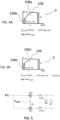
    • Figures 4A and 4B show details of pulses at two different positions on a modulating frequency curve;
    • Figure 5 is an example of simplified lock-in schematics.
    Description of Embodiments
  • It is now referred to figure 1 which shows an example of possible implementation of a driver circuit for a semiconductor switch 102 in a lower arm 100 of a half bridge having an upper arm 100' where only the semiconductor switch is represented.
  • The driver circuit comprises gate switches 121, 122 switching power supplies 123, 124 under control of a controller 101 to provide switching of the power semiconductor switch 102. In the example shown the positive power supply 123 is a 20V power supply but may be different depending of the semiconductor switch type and the negative power supply 124 is a 5V power supply that allows to block the semiconductor switch, here also such voltage may be different depending of the semiconductor switch type.
  • In the present disclosure is provided a current generator 105 providing a current Iinj such current generator being switched ON and OFF by a switch 106a driven through a modulator 106 modulating switch pulse durations.
  • The current pulses are clamped by a clamp diode 105a to provide sequences of injecting current pulses Pinj having a voltage-clamped constant amplitude Iinj, between an emitter and a gate of the power semiconductor 102.
  • The duration of the current pulses Pinj with voltage-clamped constant amplitude Iinj is modulated periodically with a frequency Fmod providing a periodic modulation of a duration of said current pulses, said current pulses causing losses modulated with said frequency Fmod.
  • An example of sequences of injecting the current pulses during operation of the semiconductor switch are shown in figure 2 while a sequence of injecting the current pulses during OFF state of the semiconductor switch are shown in figure 3.
  • Measurement of the emitter voltage Ve versus the reference voltage of the semiconductor switch is done through an analog to digital converter ADC 107 and this voltage during the current pulse is shown in figure 4A for a first pulse 3 where said voltage has a vertical part 108b caused by the internal gate resistance which is temperature-sensitive, a positive slope 108a caused by the charging of the parasitic capacitor 110 and a straight part 108 for the rest of the duration of the pulse corresponding to the Zener diode clamping voltage Vz.
  • The parameter k Tj dependent of a junction temperature Tj of the power semiconductor can be measured by acquiring the voltage response at the very early stage of the positive slope 108a in figure 4A, or 108a' in figure 4B, or by measuring two points on the positive slope 108a, 108a' and extrapolating the starting point of such slope at the starting point of the injection. Alternatively, it may be advantageous to measure the parameter k Tj as the peak value of a short pulse, typically in the range 0.01µs to 0.2µs. In this case, the pulse for measuring the parameter k Tj may be distinct from the periodically modulated pulse. In figure 4A, the constant providing the temperature dependent part of RG-int is a·Iinj=k.
  • As shown on the figure, the gate to emitter voltage VGE is equal to 20-Ve-REF during positive switching periods where the positive voltage 123 is switched by the driver switch 121.
  • This can be seen on figure 2 where are represented:
    1. a. - the semiconductor switching pulses 1, having injected current pulses 3 and the larger current pulse 4,
    2. b. - the modulating frequency F mod 2 which modulates the width of the constant current pulses;
    3. c. The VGE curve 1 of the power semiconductor showing gate voltage reductions during the on-state of the power semi-conductor, with increased reduction time when the injection duration is increased. In addition, not visible in Fig. 2, the VGE waveform during the injection reflects the temperature response. This can be seen in Figures 4A and 4B showing the voltage Ve-REF inverted with reference to VGE and where the height of the initial voltages 108b and 108b' increases between a first current injection in figure 4A and a further current injection in figure 4B. This is an important feature of the invention since the injection is both used to modulate the losses through modulating the injection duration and monitoring the temperature response reflected by the height of the initial voltage increase upon switching ON the current Iinj;
    4. d. - the VCE curve 12 of the power semiconductor showing that the on-state voltage of the semiconductor switch is increased 31, 41 during occurrences of the current pulses 3,4 causing losses in the power semiconductor. Curve 13 shows the mean losses on a switching period, such losses increasing until a peak 14 due to the peak injection duration and decreasing after such peak injection duration;
    5. e. - a first junction temperature curve 5 for a power semiconductor switch without degraded die to heatsink connection;
    6. f. - a second junction temperature curve 7 for a power semiconductor switch with a degraded die to heatsink connection.
  • As can be seen on the drawing the first junction temperature has a lower temperature peak 6 than the second junction temperature which has a higher temperature peak 8. However, the amplitude of the peak temperature may not be accurate since working conditions may affect these peak values.
  • The junction temperature Tj will evolve from the first shorter pulse 3 to the larger pulse 4 due to the modulating frequency Fmod. Such evolution is exemplified in figures 4A and 4B corresponding to the evolution of Ve-REF which is inverted with respect to VGE during the current injection pulses. In figure 4A, the smallest value of Vinj , the height of the vertical segment 108b corresponds to (Rg+Rg int)·Iinj where Rg is the external gate resistance in figure 1 and Rg int is the internal gate resistance which is variable with temperature such as Rg int= a·Tj+b where aTj·Iinj=kTj.
  • Figure 4B shows the pulse shape for the larger injection pulse 4. In such case the vertical segment 108b' is higher due to the successive increase of losses and R'g-int= a·T'j+b where aT'j·Iinj=kT'j, T'>T.
    In figures 4A and 4B the voltage Ve-REF starts at the value (Rg+ Rg int)·Iinj and increases with slopes 108a, 108a' due to the charging of the gate/emitter capacitor 110.
    When the capacitor 110 is charged, the voltage 108, 108' is constant at the Zener voltage value.
    The height of the vertical segments 108b and 108b' allow to calculate the kTj, kT'j component of Rg int which permits to determine Tj, T'j at the start of the current injection pulses 3 and 4.
  • Knowing the kTj values of the injection pulses permits to construct junction temperature curves 5 and 7 on the basis of an interpolation of the kTj values calculated for each of the injection pulses 3.
  • In one implementation of the present disclosure, the phase is extracted with a lock-in method (known by the person skilled in the art) as shown in figure 5. The temperature estimation signal kT j 5, 7 is multiplied by the modulation frequency Fmod signal 2 and a 90°C phase-shifted version of the modulation frequency Fmod signal 2 of figure 2. The results of these two multiplications are filtered with lowpass filters to reject the noise and the 4π·Fmod component and finally converted to polar coordinates R amplitude which is not used in the present disclosure and φ the phase which corresponds to the Δφ between Fmod and the kTj signal.
  • In another implementation of the present disclosure, further to the current injection an idea is to use the delay between the occurrence of a peak duration of the current pulses and the occurrence of the peak temperature, such delay being an accurate image of the degradation of the semiconductor to heatsink stack. In the exemplified situation, a good stack quality result in a lower peak temperature 6 and a higher delay 10 between occurrence of the peak duration 4 of the current injection and the peak junction temperature in the semiconductor die, while a degraded stack will provide a shorter delay between occurrence of the peak duration 4 of the current injection and the peak junction temperature 8.
  • Triggering of the measurement of the delay may be done with the peak of the Tj reconstructed curve, the starting point of the larger current injection pulse 4 or the end of such current injection pulse.
  • The measurement of the delay is done with a processor such as a microcontroller or a FPGA having analog to digital input means. Such processor may be the processor implementing the program controlling the semiconductor switch to which will be added instructions to implement the modulated current injection 106 and control of the injection switch 106a.
  • In the realization mode discussed hereabove, the current injection is done during switching of the semiconductor switch.
  • Another possible implementation is in accordance with the curves of figure 3 which correspond to a situation where the current injection pulses are applied during OFF state of the semiconductor switch. In this implementation, the losses are directly created by the gate current injected in the internal gate resistance, by Joule effect. The semiconductor switch is not necessarily switching, i.e. it can be in stand-by mode, at zero load current.
  • In such case, the modulation curve 2' provides injection pulses 3', 4' also having a modulated duration. Such pulses also provide vertical voltage segments having a height dependent on the junction temperature which increase in correspondence with the pulses duration modulated by the modulation frequency curve 2.
  • The voltage clamped constant amplitude Iinj current pulses Pinj have a limited duration to limit the voltage-clamp duration and an injection frequency Finj equal or higher than 100 kHz to be higher than a switching frequency of the power module.
  • Here, the modulation frequency Fmod is also at least one order of magnitude lower than said injection frequency Finj to provide a sufficient number.
  • If the power module comprises several power switches, the sequences are repeated on said several power semiconductors of said power module from time to time during the operational life of the power module.
  • In order to reduce noise effects, the sequences are repeated during several periods Tmod=1/Fmod and the measurements at identical injections phases are averaged, that is the first injections of different periods are averaged together, the second injections of different periods are averaged together and the p injections of different periods are averaged together. This allows for a sensitive health indication of said power module.
  • The sequences may be repeated using different injection frequencies to address different thermal interfaces within said power module. For example, depending on the power module, frequencies between 10Hz and 100Hz may be used with respect to die-attach and wire degradation, frequencies between 1 Hz and 10Hz may be used with respect to the delamination between the isolated direct bond copper (DBC) and the baseplate, and frequencies below 1 Hz may be used with respect to the degradation of the thermal interface material such as thermal grease pump-out.
  • This disclosure is not limited to the description above which are only examples. The invention encompasses every alternative that a person skilled in the art would envisage when reading this text.

Claims (15)

  1. - Method for measuring a degradation of thermal characteristics of a power module comprising sequences of:
    - injecting current pulses (Pinj), having a voltage-clamped constant amplitude (Iinj), between an emitter and a gate of a power semiconductor of such power module, a duration of said voltage-clamped constant amplitude (Iinj) current pulses (Pinj) being modulated periodically with a modulation frequency (Fmod), said current pulses causing losses modulated with said modulation frequency (Fmod),
    - measuring a parameter (k.Tj) dependent of a junction temperature (Tj) of such power semiconductor at the beginning of said current pulses,
    - measuring a phase shift (Δφ) between said modulation frequency (Fmod) and said parameter (k Tj),
    said phase shift (Δφ) providing a health indicator for the power module.
  2. - Method according to claim 1 wherein a lock-in method is used to determine said phase-shift (Δφ).
  3. - Method according to claim 1 or 2 wherein said temperature-dependent response of said power semiconductor being a junction temperature of said power semiconductor, said method comprises determining a peak injection time (tipeak) issued from said modulation frequency, and measuring said phase shift (Δφ) as being a phase shift between a peak of said modulation frequency (Fmod) and a subsequent occurrence of said peak junction temperature (Tjmax).
  4. - Method according to claim 1 wherein said temperature-dependent response of said power semiconductor being a junction temperature of said power semiconductor, said method comprises determining a peak injection time (tipeak) from said modulation frequency, and measuring said phase shift (Δφ) as being a phase shift between a start or an end of said peak injection time (tipeak) and a subsequent occurrence of said peak junction temperature (Tjmax).
  5. - Method according to any one of the preceding claims comprising providing an initial sequence of injections of said constant current (Iinj) and measuring an initial phase shift (Δφ0) in an initial operation stage of said power module, storing said initial phase shift duration as a reference for further sequences and providing further sequences of injections of said constant current (Iinj) from time to time during the operational life of the power module and wherein a current phase shift (Δφ) at said further sequences is compared to said initial phase shift (Δφ0) to provide a warning signal when said current phase shift (Δφ) is reduced to a preestablished percentage of said initial phase shift (Δφ0).
  6. - Method according to claim 5 wherein said sequences are repeated using different modulation frequencies to address different thermal interfaces within said power module.
  7. - Method according to any one of the preceding claims wherein said modulation frequency (Fmod) is sinusoidal.
  8. - Method according to any one of the preceding claims wherein injecting a constant current may have at least one of:
    - said voltage-clamped constant amplitude current (Iinj) is a current of an amplitude within the range of 20mA to 200mA.
    - said injecting a constant current has a duration of at least 0,01 µs.
    - said constant current is set to increase the conduction loss in the power semiconductor up to 40%.
  9. - Method according to any one of the preceding claims wherein injecting voltage-clamped constant amplitude (Iinj) current pulses (Pinj) is done during at least parts of successive ON states of alternances of a switching frequency (Fs) of said power semiconductor during a period of the modulation frequency.
  10. - Method according to claim 9 wherein said modulation frequency (Fmod) is at least one order of magnitude lower than said switching frequency of said power semiconductor.
  11. - Method according to any one of claims 1 to 10 wherein injecting voltage-clamped constant amplitude (Iinj) current pulses (Pinj) is done during non-switching OFF state periods of said power semiconductor.
  12. - Method according to claim 11 wherein injecting voltage-clamped constant amplitude (Iinj) current pulses (Pinj) has a limited duration to limit the voltage-clamp duration and an injection frequency (Finj) equal or higher than 100 kHz.
  13. - Method according to claim 11 or 12 wherein said modulation frequency (Fmod) is at least one order of magnitude lower than said injection frequency (Finj).
  14. - Method according to any one of the preceding claims wherein said sequences are repeated during several modulation periods being the inverse of the modulation frequency (Tmod=1/Fmod) and comprise averaging the measurements at identical injection phases to reduce noise and allow for a sensitive health indication of said power module.
  15. - Method according to any one of the preceding claims wherein said sequences are repeated on several power semiconductors of said power module from time to time during the operational life of the power module.
EP24305034.1A 2024-01-08 2024-01-08 Power module health monitoring through periodic gate current injection with variable duration Pending EP4582819A1 (en)

Priority Applications (2)

Application Number Priority Date Filing Date Title
EP24305034.1A EP4582819A1 (en) 2024-01-08 2024-01-08 Power module health monitoring through periodic gate current injection with variable duration
PCT/JP2024/080104 WO2025150459A1 (en) 2024-01-08 2024-07-02 Power module health monitoring through periodic gate current injection with variable duration

Applications Claiming Priority (1)

Application Number Priority Date Filing Date Title
EP24305034.1A EP4582819A1 (en) 2024-01-08 2024-01-08 Power module health monitoring through periodic gate current injection with variable duration

Publications (1)

Publication Number Publication Date
EP4582819A1 true EP4582819A1 (en) 2025-07-09

Family

ID=89661447

Family Applications (1)

Application Number Title Priority Date Filing Date
EP24305034.1A Pending EP4582819A1 (en) 2024-01-08 2024-01-08 Power module health monitoring through periodic gate current injection with variable duration

Country Status (2)

Country Link
EP (1) EP4582819A1 (en)
WO (1) WO2025150459A1 (en)

Cited By (1)

* Cited by examiner, † Cited by third party
Publication number Priority date Publication date Assignee Title
CN120870802A (en) * 2025-09-22 2025-10-31 浙江广芯微电子有限公司 COOLMOS aging test scheme generation method and platform

Citations (1)

* Cited by examiner, † Cited by third party
Publication number Priority date Publication date Assignee Title
WO2013187207A1 (en) * 2012-06-14 2013-12-19 三菱電機株式会社 Apparatus for detecting deterioration of power module

Patent Citations (1)

* Cited by examiner, † Cited by third party
Publication number Priority date Publication date Assignee Title
WO2013187207A1 (en) * 2012-06-14 2013-12-19 三菱電機株式会社 Apparatus for detecting deterioration of power module

Non-Patent Citations (1)

* Cited by examiner, † Cited by third party
Title
KALKER SVEN ET AL: "Degradation Diagnosis During Active Power Cycling via Frequency-Domain Thermal Impedance Spectroscopy", 2023 11TH INTERNATIONAL CONFERENCE ON POWER ELECTRONICS AND ECCE ASIA (ICPE 2023 - ECCE ASIA), THE KOREAN INSTITUTE OF POWER ELECTRONICS, 22 May 2023 (2023-05-22), pages 1342 - 1348, XP034403915, DOI: 10.23919/ICPE2023-ECCEASIA54778.2023.10213859 *

Cited By (1)

* Cited by examiner, † Cited by third party
Publication number Priority date Publication date Assignee Title
CN120870802A (en) * 2025-09-22 2025-10-31 浙江广芯微电子有限公司 COOLMOS aging test scheme generation method and platform

Also Published As

Publication number Publication date
WO2025150459A1 (en) 2025-07-17

Similar Documents

Publication Publication Date Title
US9039279B2 (en) System and method for monitoring in real time the operating state of an IGBT device
US11397209B2 (en) Methods of monitoring conditions associated with aging of silicon carbide power MOSFET devices in-situ, related circuits and computer program products
US9935577B2 (en) Semiconductor device and fault detecting method
EP2882103B1 (en) Method and apparatus for short circuit protection of power semiconductor switch
WO2019107075A1 (en) Diagnostic device and method to establish degradation state of electrical connection in power semiconductor device
US9285400B2 (en) Method for determining current in a polyphase machine
Li et al. Accurate measurement of dynamic on-state resistances of GaN devices under reverse and forward conduction in high frequency power converter
WO2025150459A1 (en) Power module health monitoring through periodic gate current injection with variable duration
Anurag et al. An accurate calorimetric method for measurement of switching losses in silicon carbide (SiC) MOSFETs
CN119199443B (en) Method for setting relation between conduction voltage drop and junction temperature of power device in high-current switch state
JP7858781B2 (en) Semiconductor devices and power converters
Du et al. A measurement method to extract the transient junction temperature profile of power semiconductors at surge conditions
WO2019198775A1 (en) Diagnostic device and diagnostic system
JP6754438B2 (en) Electrical equipment and diagnostic equipment for electrical equipment
WO2018168116A1 (en) Power conversion device diagnosis circuit and power conversion device diagnosis system
Krone et al. Advanced condition monitoring system based on on-line semiconductor loss measurements
Barón et al. Characterization of electrical parameters for health monitoring in sic mosfets during ac power cycling
JP2019060792A (en) Power converter diagnostic circuit and diagnostic system
US11736000B2 (en) Power converter with thermal resistance monitoring
US12607585B2 (en) Method for measuring degradation of thermal resistance between power semiconductor and heat sink, and control device for power semiconductor
Yu et al. Review on condition monitoring methods of IGBT power device
Felgemacher et al. IGBT online-temperature monitoring using turn-off delay as a temperature sensitive electrical parameter
Leung et al. Accelerated power cycling of gan hemts using switching loss and fast temperature measurement
Vogt et al. Condition monitoring of a GaN full-bridge by means of forward voltage measurements in continuous operation
Khadka et al. Body-Diode Reliability Characterization of Silicon Carbide MOSFETs Toward a Degradation-Insensitive Online Junction Temperature Monitoring

Legal Events

Date Code Title Description
PUAI Public reference made under article 153(3) epc to a published international application that has entered the european phase

Free format text: ORIGINAL CODE: 0009012

STAA Information on the status of an ep patent application or granted ep patent

Free format text: STATUS: THE APPLICATION HAS BEEN PUBLISHED

AK Designated contracting states

Kind code of ref document: A1

Designated state(s): AL AT BE BG CH CY CZ DE DK EE ES FI FR GB GR HR HU IE IS IT LI LT LU LV MC ME MK MT NL NO PL PT RO RS SE SI SK SM TR

STAA Information on the status of an ep patent application or granted ep patent

Free format text: STATUS: REQUEST FOR EXAMINATION WAS MADE

17P Request for examination filed

Effective date: 20251009