EP4580341A2 - Directed self assembly-enabled back-side contact arrays aligned to gate electrodes - Google Patents
Directed self assembly-enabled back-side contact arrays aligned to gate electrodes Download PDFInfo
- Publication number
- EP4580341A2 EP4580341A2 EP24210829.8A EP24210829A EP4580341A2 EP 4580341 A2 EP4580341 A2 EP 4580341A2 EP 24210829 A EP24210829 A EP 24210829A EP 4580341 A2 EP4580341 A2 EP 4580341A2
- Authority
- EP
- European Patent Office
- Prior art keywords
- gate
- dielectric
- sidewall
- nanoribbons
- metallization
- Prior art date
- Legal status (The legal status is an assumption and is not a legal conclusion. Google has not performed a legal analysis and makes no representation as to the accuracy of the status listed.)
- Pending
Links
Images





Classifications
-
- H—ELECTRICITY
- H10—SEMICONDUCTOR DEVICES; ELECTRIC SOLID-STATE DEVICES NOT OTHERWISE PROVIDED FOR
- H10D—INORGANIC ELECTRIC SEMICONDUCTOR DEVICES
- H10D84/00—Integrated devices formed in or on semiconductor substrates that comprise only semiconducting layers, e.g. on Si wafers or on GaAs-on-Si wafers
- H10D84/01—Manufacture or treatment
- H10D84/0123—Integrating together multiple components covered by H10D12/00 or H10D30/00, e.g. integrating multiple IGBTs
- H10D84/0126—Integrating together multiple components covered by H10D12/00 or H10D30/00, e.g. integrating multiple IGBTs the components including insulated gates, e.g. IGFETs
- H10D84/0149—Manufacturing their interconnections or electrodes, e.g. source or drain electrodes
-
- H—ELECTRICITY
- H10—SEMICONDUCTOR DEVICES; ELECTRIC SOLID-STATE DEVICES NOT OTHERWISE PROVIDED FOR
- H10D—INORGANIC ELECTRIC SEMICONDUCTOR DEVICES
- H10D30/00—Field-effect transistors [FET]
- H10D30/01—Manufacture or treatment
- H10D30/014—Manufacture or treatment of FETs having zero-dimensional [0D] or one-dimensional [1D] channels, e.g. quantum wire FETs, single-electron transistors [SET] or Coulomb blockade transistors
-
- H—ELECTRICITY
- H10—SEMICONDUCTOR DEVICES; ELECTRIC SOLID-STATE DEVICES NOT OTHERWISE PROVIDED FOR
- H10D—INORGANIC ELECTRIC SEMICONDUCTOR DEVICES
- H10D30/00—Field-effect transistors [FET]
- H10D30/01—Manufacture or treatment
- H10D30/019—Manufacture or treatment of FETs having stacked nanowire, nanosheet or nanoribbon channels
- H10D30/0198—Manufacture or treatment of FETs having stacked nanowire, nanosheet or nanoribbon channels forming source or drain electrodes wherein semiconductor bodies are replaced by dielectric layers and the source or drain electrodes extend through the dielectric layers
-
- H—ELECTRICITY
- H10—SEMICONDUCTOR DEVICES; ELECTRIC SOLID-STATE DEVICES NOT OTHERWISE PROVIDED FOR
- H10D—INORGANIC ELECTRIC SEMICONDUCTOR DEVICES
- H10D30/00—Field-effect transistors [FET]
- H10D30/40—FETs having zero-dimensional [0D], one-dimensional [1D] or two-dimensional [2D] charge carrier gas channels
- H10D30/43—FETs having zero-dimensional [0D], one-dimensional [1D] or two-dimensional [2D] charge carrier gas channels having one-dimensional [1D] charge carrier gas channels, e.g. quantum wire FETs or transistors having 1D quantum-confined channels
-
- H—ELECTRICITY
- H10—SEMICONDUCTOR DEVICES; ELECTRIC SOLID-STATE DEVICES NOT OTHERWISE PROVIDED FOR
- H10D—INORGANIC ELECTRIC SEMICONDUCTOR DEVICES
- H10D30/00—Field-effect transistors [FET]
- H10D30/501—FETs having stacked nanowire, nanosheet or nanoribbon channels
-
- H—ELECTRICITY
- H10—SEMICONDUCTOR DEVICES; ELECTRIC SOLID-STATE DEVICES NOT OTHERWISE PROVIDED FOR
- H10D—INORGANIC ELECTRIC SEMICONDUCTOR DEVICES
- H10D30/00—Field-effect transistors [FET]
- H10D30/60—Insulated-gate field-effect transistors [IGFET]
- H10D30/67—Thin-film transistors [TFT]
- H10D30/6729—Thin-film transistors [TFT] characterised by the electrodes
- H10D30/673—Thin-film transistors [TFT] characterised by the electrodes characterised by the shapes, relative sizes or dispositions of the gate electrodes
- H10D30/6735—Thin-film transistors [TFT] characterised by the electrodes characterised by the shapes, relative sizes or dispositions of the gate electrodes having gates fully surrounding the channels, e.g. gate-all-around
-
- H—ELECTRICITY
- H10—SEMICONDUCTOR DEVICES; ELECTRIC SOLID-STATE DEVICES NOT OTHERWISE PROVIDED FOR
- H10D—INORGANIC ELECTRIC SEMICONDUCTOR DEVICES
- H10D30/00—Field-effect transistors [FET]
- H10D30/60—Insulated-gate field-effect transistors [IGFET]
- H10D30/67—Thin-film transistors [TFT]
- H10D30/6757—Thin-film transistors [TFT] characterised by the structure of the channel, e.g. transverse or longitudinal shape or doping profile
-
- H—ELECTRICITY
- H10—SEMICONDUCTOR DEVICES; ELECTRIC SOLID-STATE DEVICES NOT OTHERWISE PROVIDED FOR
- H10D—INORGANIC ELECTRIC SEMICONDUCTOR DEVICES
- H10D62/00—Semiconductor bodies, or regions thereof, of devices having potential barriers
- H10D62/10—Shapes, relative sizes or dispositions of the regions of the semiconductor bodies; Shapes of the semiconductor bodies
- H10D62/117—Shapes of semiconductor bodies
- H10D62/118—Nanostructure semiconductor bodies
- H10D62/119—Nanowire, nanosheet or nanotube semiconductor bodies
- H10D62/121—Nanowire, nanosheet or nanotube semiconductor bodies oriented parallel to substrates
-
- H—ELECTRICITY
- H10—SEMICONDUCTOR DEVICES; ELECTRIC SOLID-STATE DEVICES NOT OTHERWISE PROVIDED FOR
- H10D—INORGANIC ELECTRIC SEMICONDUCTOR DEVICES
- H10D64/00—Electrodes of devices having potential barriers
- H10D64/01—Manufacture or treatment
-
- H—ELECTRICITY
- H10—SEMICONDUCTOR DEVICES; ELECTRIC SOLID-STATE DEVICES NOT OTHERWISE PROVIDED FOR
- H10D—INORGANIC ELECTRIC SEMICONDUCTOR DEVICES
- H10D64/00—Electrodes of devices having potential barriers
- H10D64/20—Electrodes characterised by their shapes, relative sizes or dispositions
- H10D64/23—Electrodes carrying the current to be rectified, amplified, oscillated or switched, e.g. sources, drains, anodes or cathodes
- H10D64/251—Source or drain electrodes for field-effect devices
-
- H—ELECTRICITY
- H10—SEMICONDUCTOR DEVICES; ELECTRIC SOLID-STATE DEVICES NOT OTHERWISE PROVIDED FOR
- H10D—INORGANIC ELECTRIC SEMICONDUCTOR DEVICES
- H10D64/00—Electrodes of devices having potential barriers
- H10D64/20—Electrodes characterised by their shapes, relative sizes or dispositions
- H10D64/23—Electrodes carrying the current to be rectified, amplified, oscillated or switched, e.g. sources, drains, anodes or cathodes
- H10D64/251—Source or drain electrodes for field-effect devices
- H10D64/258—Source or drain electrodes for field-effect devices characterised by the relative positions of the source or drain electrodes with respect to the gate electrode
-
- H—ELECTRICITY
- H10—SEMICONDUCTOR DEVICES; ELECTRIC SOLID-STATE DEVICES NOT OTHERWISE PROVIDED FOR
- H10D—INORGANIC ELECTRIC SEMICONDUCTOR DEVICES
- H10D64/00—Electrodes of devices having potential barriers
- H10D64/20—Electrodes characterised by their shapes, relative sizes or dispositions
- H10D64/27—Electrodes not carrying the current to be rectified, amplified, oscillated or switched, e.g. gates
- H10D64/311—Gate electrodes for field-effect devices
- H10D64/411—Gate electrodes for field-effect devices for FETs
- H10D64/511—Gate electrodes for field-effect devices for FETs for IGFETs
- H10D64/517—Gate electrodes for field-effect devices for FETs for IGFETs characterised by the conducting layers
- H10D64/518—Gate electrodes for field-effect devices for FETs for IGFETs characterised by the conducting layers characterised by their lengths or sectional shapes
-
- H—ELECTRICITY
- H10—SEMICONDUCTOR DEVICES; ELECTRIC SOLID-STATE DEVICES NOT OTHERWISE PROVIDED FOR
- H10D—INORGANIC ELECTRIC SEMICONDUCTOR DEVICES
- H10D84/00—Integrated devices formed in or on semiconductor substrates that comprise only semiconducting layers, e.g. on Si wafers or on GaAs-on-Si wafers
- H10D84/80—Integrated devices formed in or on semiconductor substrates that comprise only semiconducting layers, e.g. on Si wafers or on GaAs-on-Si wafers characterised by the integration of at least one component covered by groups H10D12/00 or H10D30/00, e.g. integration of IGFETs
- H10D84/82—Integrated devices formed in or on semiconductor substrates that comprise only semiconducting layers, e.g. on Si wafers or on GaAs-on-Si wafers characterised by the integration of at least one component covered by groups H10D12/00 or H10D30/00, e.g. integration of IGFETs of only field-effect components
- H10D84/83—Integrated devices formed in or on semiconductor substrates that comprise only semiconducting layers, e.g. on Si wafers or on GaAs-on-Si wafers characterised by the integration of at least one component covered by groups H10D12/00 or H10D30/00, e.g. integration of IGFETs of only field-effect components of only insulated-gate FETs [IGFET]
-
- H—ELECTRICITY
- H10—SEMICONDUCTOR DEVICES; ELECTRIC SOLID-STATE DEVICES NOT OTHERWISE PROVIDED FOR
- H10D—INORGANIC ELECTRIC SEMICONDUCTOR DEVICES
- H10D84/00—Integrated devices formed in or on semiconductor substrates that comprise only semiconducting layers, e.g. on Si wafers or on GaAs-on-Si wafers
- H10D84/80—Integrated devices formed in or on semiconductor substrates that comprise only semiconducting layers, e.g. on Si wafers or on GaAs-on-Si wafers characterised by the integration of at least one component covered by groups H10D12/00 or H10D30/00, e.g. integration of IGFETs
- H10D84/82—Integrated devices formed in or on semiconductor substrates that comprise only semiconducting layers, e.g. on Si wafers or on GaAs-on-Si wafers characterised by the integration of at least one component covered by groups H10D12/00 or H10D30/00, e.g. integration of IGFETs of only field-effect components
- H10D84/83—Integrated devices formed in or on semiconductor substrates that comprise only semiconducting layers, e.g. on Si wafers or on GaAs-on-Si wafers characterised by the integration of at least one component covered by groups H10D12/00 or H10D30/00, e.g. integration of IGFETs of only field-effect components of only insulated-gate FETs [IGFET]
- H10D84/832—Integrated devices formed in or on semiconductor substrates that comprise only semiconducting layers, e.g. on Si wafers or on GaAs-on-Si wafers characterised by the integration of at least one component covered by groups H10D12/00 or H10D30/00, e.g. integration of IGFETs of only field-effect components of only insulated-gate FETs [IGFET] comprising IGFETs having stacked nanowire, nanosheet or nanoribbon channels
-
- H—ELECTRICITY
- H10—SEMICONDUCTOR DEVICES; ELECTRIC SOLID-STATE DEVICES NOT OTHERWISE PROVIDED FOR
- H10W—GENERIC PACKAGES, INTERCONNECTIONS, CONNECTORS OR OTHER CONSTRUCTIONAL DETAILS OF DEVICES COVERED BY CLASS H10
- H10W20/00—Interconnections in chips, wafers or substrates
- H10W20/01—Manufacture or treatment
- H10W20/031—Manufacture or treatment of conductive parts of the interconnections
- H10W20/069—Manufacture or treatment of conductive parts of the interconnections by forming self-aligned vias or self-aligned contact plugs
-
- H—ELECTRICITY
- H10—SEMICONDUCTOR DEVICES; ELECTRIC SOLID-STATE DEVICES NOT OTHERWISE PROVIDED FOR
- H10W—GENERIC PACKAGES, INTERCONNECTIONS, CONNECTORS OR OTHER CONSTRUCTIONAL DETAILS OF DEVICES COVERED BY CLASS H10
- H10W20/00—Interconnections in chips, wafers or substrates
- H10W20/40—Interconnections external to wafers or substrates, e.g. back-end-of-line [BEOL] metallisations or vias connecting to gate electrodes
- H10W20/41—Interconnections external to wafers or substrates, e.g. back-end-of-line [BEOL] metallisations or vias connecting to gate electrodes characterised by their conductive parts
- H10W20/427—Power or ground buses
-
- H—ELECTRICITY
- H10—SEMICONDUCTOR DEVICES; ELECTRIC SOLID-STATE DEVICES NOT OTHERWISE PROVIDED FOR
- H10W—GENERIC PACKAGES, INTERCONNECTIONS, CONNECTORS OR OTHER CONSTRUCTIONAL DETAILS OF DEVICES COVERED BY CLASS H10
- H10W20/00—Interconnections in chips, wafers or substrates
- H10W20/40—Interconnections external to wafers or substrates, e.g. back-end-of-line [BEOL] metallisations or vias connecting to gate electrodes
- H10W20/41—Interconnections external to wafers or substrates, e.g. back-end-of-line [BEOL] metallisations or vias connecting to gate electrodes characterised by their conductive parts
- H10W20/43—Layouts of interconnections
-
- B—PERFORMING OPERATIONS; TRANSPORTING
- B82—NANOTECHNOLOGY
- B82Y—SPECIFIC USES OR APPLICATIONS OF NANOSTRUCTURES; MEASUREMENT OR ANALYSIS OF NANOSTRUCTURES; MANUFACTURE OR TREATMENT OF NANOSTRUCTURES
- B82Y10/00—Nanotechnology for information processing, storage or transmission, e.g. quantum computing or single electron logic
-
- H—ELECTRICITY
- H10—SEMICONDUCTOR DEVICES; ELECTRIC SOLID-STATE DEVICES NOT OTHERWISE PROVIDED FOR
- H10D—INORGANIC ELECTRIC SEMICONDUCTOR DEVICES
- H10D64/00—Electrodes of devices having potential barriers
- H10D64/20—Electrodes characterised by their shapes, relative sizes or dispositions
- H10D64/27—Electrodes not carrying the current to be rectified, amplified, oscillated or switched, e.g. gates
- H10D64/311—Gate electrodes for field-effect devices
- H10D64/411—Gate electrodes for field-effect devices for FETs
- H10D64/511—Gate electrodes for field-effect devices for FETs for IGFETs
- H10D64/517—Gate electrodes for field-effect devices for FETs for IGFETs characterised by the conducting layers
-
- H—ELECTRICITY
- H10—SEMICONDUCTOR DEVICES; ELECTRIC SOLID-STATE DEVICES NOT OTHERWISE PROVIDED FOR
- H10D—INORGANIC ELECTRIC SEMICONDUCTOR DEVICES
- H10D84/00—Integrated devices formed in or on semiconductor substrates that comprise only semiconducting layers, e.g. on Si wafers or on GaAs-on-Si wafers
- H10D84/01—Manufacture or treatment
- H10D84/02—Manufacture or treatment characterised by using material-based technologies
- H10D84/03—Manufacture or treatment characterised by using material-based technologies using Group IV technology, e.g. silicon technology or silicon-carbide [SiC] technology
- H10D84/038—Manufacture or treatment characterised by using material-based technologies using Group IV technology, e.g. silicon technology or silicon-carbide [SiC] technology using silicon technology, e.g. SiGe
Definitions
- back-side contacts and/or gate vias are limited, sometimes severely, by edge placement errors between back-side patterns and front-side features.
- Typical patterning misalignments may be dwarfed by wafer distortions at least along certain orientations. Such misalignments may significantly degrade integrated circuit (IC) device performance or prevent further down-scaling of transistor arrays.
- IC integrated circuit
- references within this specification to "one embodiment” or “an embodiment” mean that a particular feature, structure, or characteristic described in connection with the embodiment is included in at least one implementation encompassed within the present description. Therefore, the use of the phrase “one embodiment” or “in an embodiment” does not necessarily refer to the same embodiment.
- the location or arrangement of individual elements within each disclosed embodiment may be modified without departing from the spirit and scope of the claimed subject matter. The following detailed description is, therefore, not to be taken in a limiting sense, and the scope of the subject matter is defined only by the appended claims, appropriately interpreted, along with the full range of equivalents to which the appended claims are entitled.
- over may refer to a relative position of one layer with respect to other layers.
- One layer “over” or “on” another layer or bonded “to” another layer may be directly in contact with the other layer or may have one or more intervening layers.
- One layer “between” layers may be directly in contact with the layers or may have one or more intervening layers.
- Coupled may be used to indicate that two or more elements are in direct physical or electrical contact with each other.
- Connected may be used to indicate that two or more elements are in direct physical or electrical contact with each other.
- Connected may be used to indicate that two or more elements are in either direct or indirect (with other intervening elements between them) physical or electrical contact with each other, and/or that the two or more elements co-operate or interact with each other (e.g., as in a cause-and-effect relationship, an electrical relationship, a functional relationship, etc.).
- circuit or “module” may refer to one or more passive and/or active components that are arranged to cooperate with one another to provide a desired function.
- signal may refer to at least one current signal, voltage signal, magnetic signal, or data/clock signal.
- the terms “substantially,” “close,” “approximately,” “near,” and “about,” generally refer to being within +/- 10% of a target value (unless specifically specified).
- the term “predominantly” means more than 50%, or more than half.
- a composition that is predominantly a first constituent means more than half of the composition is the first constituent.
- the term “primarily” means the most, or greatest, part.
- a composition that is primarily a first constituent means the composition has more of the first constituent than any other constituent.
- a composition that is primarily first and second constituents means the composition has more of the first and second constituents than any other constituent.
- phrases “A and/or B” and “A or B” mean (A), (B), or (A and B).
- phrase “A, B, and/or C” means (A), (B), (C), (A and B), (A and C), (B and C), or (A, B and C).
- cross-sectional Views labeled "cross-sectional,” “profile,” and “plan” correspond to orthogonal planes within a cartesian coordinate system. Thus, cross-sectional and profile views are taken in the x-z and y-z planes, and plan views are taken in the x-y plane. Typically, profile views in the x-z plane are cross-sectional views. Where appropriate, drawings are labeled with axes to indicate the orientation of the figure.
- Materials, structures, and techniques are disclosed to improve the alignment and scaling of integrated circuit (IC) devices having transistors between and coupled to front- and back-side interconnect networks.
- IC integrated circuit
- Typical patterning methods may be insufficiently precise to properly align front- and back-side features in IC devices, particularly given the nonstop scaling down of devices.
- a method is described to form back-side arrays of sacrificial materials precisely aligned to transistor structures formed on a front side.
- Directed self-assembly may be used to form an array or grating of contacts and dielectric structures on a back side to precisely match a similar array on a front side.
- the DSA grating may be aligned with transistor gate electrodes revealed on the back side and allow for further self-aligned back-side contacts and vias.
- Self-alignment may be limited to a single, key dimension (e.g., parallel to a longitudinal direction of a channel region).
- described structures may include gate electrodes with thick bottoms to facilitate back-side reveal and subsequent alignment.
- FIG. 1 is a flow chart of methods 100 for forming an array of back-side contacts and dielectric structures aligned with transistor gate electrodes, in accordance with some embodiments.
- Methods 100 include operations 101-110. Some operations shown in FIG. 1 are optional. Additional operations may be included. FIG. 1 shows an example sequence, but the operations can be done in other orders as well, and some operations may be omitted. Some operations can also be performed multiple times before other operations are performed. Some operations may be included within other operations so that the number of operations illustrated FIG. 1 is not a limitation of the methods 100.
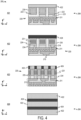
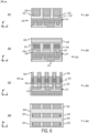
- FIGS. 2 , 3 , 4 , 5 , 6 , 7 , 8 , and 9 illustrate cross-sectional profile views of transistor structures between and coupled to front- and back-side interconnect layers, at various stages of manufacture, in accordance with some embodiments.
- FIGS. 2-9 show possible examples of intermediate structures during an embodiment of a practice of methods 100 of FIG. 1 .
- the substrate has multiple transistor structures (e.g., in extensive arrays), and the multiple transistor structures are coupled to an interconnect network (e.g., on a front side) over the transistor structures.
- the transistor structures each include channel regions between source and drain regions and gate electrodes over the channel regions and between the source and drain regions.
- the channels regions may be in any suitable structures, such as nanoribbons, fins, etc.
- Nanoribbons may be in a stack of mechanically and electrically parallel nanoribbons between the source and drain regions. Nanoribbons may be of any suitable width or length. Some nanoribbons may have dimensions fitting nanowires or nanosheets.
- the substrate may include any suitable material or materials. Any suitable semiconductor or other material can be used.
- the substrate may be any suitable substrate, such as a wafer, die, etc.
- the substrate may include a semiconductor material that transistors can be formed out of and on, including a crystalline material, such as monocrystalline or polycrystalline silicon (Si), germanium (Ge), silicon germanium (SiGe), a III-V alloy material (e.g., gallium arsenide (GaAs)), a silicon carbide (SiC), a sapphire (Al 2 O 3 ), or any combination thereof.
- the substrate includes crystalline silicon and subsequent components are also silicon.
- the substrate may be a silicon-on-insulator (SOI) substrate.
- Communication chip 1307 may operate in accordance with Code Division Multiple Access (CDMA), Time Division Multiple Access (TDMA), Digital Enhanced Cordless Telecommunications (DECT), Evolution-Data Optimized (EV-DO), and derivatives thereof, as well as any other wireless protocols that are designated as 3G, 4G, 5G, and beyond.
- Communication chip 1307 may operate in accordance with other wireless protocols in other embodiments.
- Computing device 1300 may include an antenna 1313 to facilitate wireless communications and/or to receive other wireless communications (such as AM or FM radio transmissions).
- communication chip 1307 may manage wired communications, such as electrical, optical, or any other suitable communication protocols (e.g., the Ethernet). As noted above, communication chip 1307 may include multiple communication chips. For instance, a first communication chip 1307 may be dedicated to shorter-range wireless communications such as Wi-Fi or Bluetooth, and a second communication chip 1307 may be dedicated to longer-range wireless communications such as GPS, EDGE, GPRS, CDMA, WiMAX, LTE, EV-DO, or others. In some embodiments, a first communication chip 1307 may be dedicated to wireless communications, and a second communication chip 1307 may be dedicated to wired communications.
- wired communications such as electrical, optical, or any other suitable communication protocols (e.g., the Ethernet).
- communication chip 1307 may include multiple communication chips. For instance, a first communication chip 1307 may be dedicated to shorter-range wireless communications such as Wi-Fi or Bluetooth, and a second communication chip 1307 may be dedicated to longer-range wireless communications such as GPS, EDGE, GPRS, CDMA, WiMAX
- Computing device 1300 may include battery/power circuitry 1308.
- Battery/power circuitry 1308 may include one or more energy storage devices (e.g., batteries or capacitors) and/or circuitry for coupling components of computing device 1300 to an energy source separate from computing device 1300 (e.g., AC line power).
- Computing device 1300 may include an audio output device 1304 (or corresponding interface circuitry, as discussed above). Audio output device 1304 may include any device that generates an audible indicator, such as speakers, headsets, or earbuds, for example.
- Computing device 1300 may include an audio input device 1310 (or corresponding interface circuitry, as discussed above). Audio input device 1310 may include any device that generates a signal representative of a sound, such as microphones, microphone arrays, or digital instruments (e.g., instruments having a musical instrument digital interface (MIDI) output).
- Audio input device 1310 may include any device that generates a signal representative of a sound, such as microphones, microphone arrays, or digital instruments (e.g., instruments having a musical instrument digital interface (MIDI) output).
- MIDI musical instrument digital interface
- Computing device 1300 may include a GPS device 1309 (or corresponding interface circuitry, as discussed above). GPS device 1309 may be in communication with a satellite-based system and may receive a location of computing device 1300, as known in the art.
- Computing device 1300 may include other output device 1305 (or corresponding interface circuitry, as discussed above).
- Examples of the other output device 1305 may include an audio codec, a video codec, a printer, a wired or wireless transmitter for providing information to other devices, or an additional storage device.
- Computing device 1300 may include other input device 1311 (or corresponding interface circuitry, as discussed above).
- Examples of the other input device 1311 may include an accelerometer, a gyroscope, a compass, an image capture device, a keyboard, a cursor control device such as a mouse, a stylus, a touchpad, a bar code reader, a Quick Response (QR) code reader, any sensor, or a radio frequency identification (RFID) reader.
- RFID radio frequency identification
- Computing device 1300 may include a security interface device 1312.
- Security interface device 1312 may include any device that provides security measures for computing device 1300 such as intrusion detection, biometric validation, security encode or decode, access list management, malware detection, or spyware detection.
- an apparatus in one or more first embodiments, includes first and second metallization layers, and a transistor structure including a stack of nanoribbons between and coupling first and second impurity doped regions, and a gate electrode adjacent the nanoribbons, wherein the first metallization layer is over and coupled to the first impurity doped region, the second impurity doped region is over and coupled to the second metallization layer, and a first vertical pitch between a lowest of the nanoribbons and a lowest surface of the gate electrode is greater than one-and-a-half times a second vertical pitch between the lowest of the nanoribbons and a next lowest of the nanoribbons.
- the first vertical pitch is greater than twice the second vertical pitch.
- the first vertical pitch is greater than 20 nm.
- the apparatus also includes a first dielectric structure on the gate electrode and between the first metallization layer and the gate electrode, and a second dielectric structure on the gate electrode and between the gate electrode and the second metallization layer, wherein a first sidewall of the first dielectric structure is substantially vertically aligned over a second sidewall of the second dielectric structure, and a third sidewall of the first dielectric structure is substantially vertically aligned over a fourth sidewall of the second dielectric structure.
- the first sidewall is precisely vertically aligned over the second sidewall
- the third sidewall is precisely vertically aligned over the fourth sidewall
Landscapes
- Electrodes Of Semiconductors (AREA)
- Physics & Mathematics (AREA)
- Geometry (AREA)
- Metal-Oxide And Bipolar Metal-Oxide Semiconductor Integrated Circuits (AREA)
- Thin Film Transistor (AREA)
Abstract
Description
- Formation of back-side contacts and/or gate vias is limited, sometimes severely, by edge placement errors between back-side patterns and front-side features. Typical patterning misalignments may be dwarfed by wafer distortions at least along certain orientations. Such misalignments may significantly degrade integrated circuit (IC) device performance or prevent further down-scaling of transistor arrays.
- New techniques, structures, and materials are needed to improve front- and back-side feature alignments.
- The material described herein is illustrated by way of example and not by way of limitation in the accompanying figures. For simplicity and clarity of illustration, elements illustrated in the figures are not necessarily drawn to scale. For example, the dimensions of some elements may be exaggerated relative to other elements for clarity. Further, where considered appropriate, reference labels have been repeated among the figures to indicate corresponding or analogous elements, e.g., with the same or similar functionality. The disclosure will be described with additional specificity and detail through use of the accompanying drawings:
-
FIG. 1 is a flow chart of methods for forming an array of back-side contacts and dielectric structures aligned with transistor gate electrodes, in accordance with some embodiments; -
FIGS. 2 ,3 ,4 ,5 ,6 ,7 ,8 , and9 illustrate cross-sectional profile views of transistor structures between and coupled to front- and back-side interconnect layers, at various stages of manufacture, in accordance with some embodiments; -
FIGS. 10A and10B illustrate cross-sectional profile views of an integrated circuit (IC) device having transistor structures between and coupled to front- and back-side layers in frontand back-side interconnect networks, in accordance with some embodiments; -
FIG. 11 illustrates a cross-sectional profile view of an IC system having transistor structures with front- and back-side contacts and vias to front- and back-side interconnect layers, in accordance with some embodiments; -
FIG. 12 illustrates a diagram of an example data server machine employing an IC device having back-side contacts through self-aligned dielectric layers, in accordance with some embodiments; and -
FIG. 13 is a block diagram of an example computing device, in accordance with some embodiments. - In the following detailed description, reference is made to the accompanying drawings that show, by way of illustration, specific embodiments in which the claimed subject matter may be practiced. These embodiments are described in sufficient detail to enable those skilled in the art to practice the subject matter. The various embodiments, although different, are not necessarily mutually exclusive. For example, a particular feature, structure, or characteristic described herein, in connection with one embodiment, may be implemented within other embodiments without departing from the spirit and scope of the claimed subject matter.
- References within this specification to "one embodiment" or "an embodiment" mean that a particular feature, structure, or characteristic described in connection with the embodiment is included in at least one implementation encompassed within the present description. Therefore, the use of the phrase "one embodiment" or "in an embodiment" does not necessarily refer to the same embodiment. In addition, the location or arrangement of individual elements within each disclosed embodiment may be modified without departing from the spirit and scope of the claimed subject matter. The following detailed description is, therefore, not to be taken in a limiting sense, and the scope of the subject matter is defined only by the appended claims, appropriately interpreted, along with the full range of equivalents to which the appended claims are entitled.
- The terms "over," "to," "between," and "on" as used herein may refer to a relative position of one layer with respect to other layers. One layer "over" or "on" another layer or bonded "to" another layer may be directly in contact with the other layer or may have one or more intervening layers. One layer "between" layers may be directly in contact with the layers or may have one or more intervening layers.
- The terms "coupled" and "connected," along with their derivatives, may be used herein to describe structural relationships between components. These terms are not intended as synonyms for each other. Rather, in particular embodiments, "connected" may be used to indicate that two or more elements are in direct physical or electrical contact with each other. "Coupled" may be used to indicate that two or more elements are in either direct or indirect (with other intervening elements between them) physical or electrical contact with each other, and/or that the two or more elements co-operate or interact with each other (e.g., as in a cause-and-effect relationship, an electrical relationship, a functional relationship, etc.).
- The term "circuit" or "module" may refer to one or more passive and/or active components that are arranged to cooperate with one another to provide a desired function. The term "signal" may refer to at least one current signal, voltage signal, magnetic signal, or data/clock signal. The meaning of "a," "an," and "the" include plural references. The meaning of "in" includes "in" and "on."
- The vertical orientation is in the z-direction and recitations of "top," "bottom," "above," and "below" refer to relative positions in the z-dimension with the usual meaning. However, embodiments are not necessarily limited to the orientations or configurations illustrated in the figure.
- The terms "substantially," "close," "approximately," "near," and "about," generally refer to being within +/- 10% of a target value (unless specifically specified). Unless otherwise specified in the specific context of use, the term "predominantly" means more than 50%, or more than half. For example, a composition that is predominantly a first constituent means more than half of the composition is the first constituent. The term "primarily" means the most, or greatest, part. For example, a composition that is primarily a first constituent means the composition has more of the first constituent than any other constituent. A composition that is primarily first and second constituents means the composition has more of the first and second constituents than any other constituent.
- Unless otherwise specified the use of the ordinal adjectives "first," "second," and "third," etc., to describe a common object, merely indicate that different instances of like objects to which are being referred and are not intended to imply that the objects so described must be in a given sequence, either temporally, spatially, in ranking or in any other manner.
- For the purposes of the present disclosure, phrases "A and/or B" and "A or B" mean (A), (B), or (A and B). For the purposes of the present disclosure, the phrase "A, B, and/or C" means (A), (B), (C), (A and B), (A and C), (B and C), or (A, B and C).
- Views labeled "cross-sectional," "profile," and "plan" correspond to orthogonal planes within a cartesian coordinate system. Thus, cross-sectional and profile views are taken in the x-z and y-z planes, and plan views are taken in the x-y plane. Typically, profile views in the x-z plane are cross-sectional views. Where appropriate, drawings are labeled with axes to indicate the orientation of the figure.
- Materials, structures, and techniques are disclosed to improve the alignment and scaling of integrated circuit (IC) devices having transistors between and coupled to front- and back-side interconnect networks.
- Typical patterning methods may be insufficiently precise to properly align front- and back-side features in IC devices, particularly given the nonstop scaling down of devices. A method is described to form back-side arrays of sacrificial materials precisely aligned to transistor structures formed on a front side. Directed self-assembly (DSA) may be used to form an array or grating of contacts and dielectric structures on a back side to precisely match a similar array on a front side. The DSA grating may be aligned with transistor gate electrodes revealed on the back side and allow for further self-aligned back-side contacts and vias. Self-alignment may be limited to a single, key dimension (e.g., parallel to a longitudinal direction of a channel region).
- Such self-aligned features enable back-side interconnects with continued device scaling. In addition to near-perfect alignment between front- and back-side features (e.g., front- and backside spacer layers), described structures may include gate electrodes with thick bottoms to facilitate back-side reveal and subsequent alignment.
-
FIG. 1 is a flow chart of methods 100 for forming an array of back-side contacts and dielectric structures aligned with transistor gate electrodes, in accordance with some embodiments. Methods 100 include operations 101-110. Some operations shown inFIG. 1 are optional. Additional operations may be included.FIG. 1 shows an example sequence, but the operations can be done in other orders as well, and some operations may be omitted. Some operations can also be performed multiple times before other operations are performed. Some operations may be included within other operations so that the number of operations illustratedFIG. 1 is not a limitation of the methods 100. -
FIGS. 2 ,3 ,4 ,5 ,6 ,7 ,8 , and9 illustrate cross-sectional profile views of transistor structures between and coupled to front- and back-side interconnect layers, at various stages of manufacture, in accordance with some embodiments.FIGS. 2-9 show possible examples of intermediate structures during an embodiment of a practice of methods 100 ofFIG. 1 . - Returning to
FIG. 1 , methods 100 begin atoperation 101 with receiving a substrate. In some embodiments, the substrate has multiple transistor structures (e.g., in extensive arrays), and the multiple transistor structures are coupled to an interconnect network (e.g., on a front side) over the transistor structures. The transistor structures each include channel regions between source and drain regions and gate electrodes over the channel regions and between the source and drain regions. The channels regions may be in any suitable structures, such as nanoribbons, fins, etc. Nanoribbons may be in a stack of mechanically and electrically parallel nanoribbons between the source and drain regions. Nanoribbons may be of any suitable width or length. Some nanoribbons may have dimensions fitting nanowires or nanosheets. - Notably, the gate electrode may be received (or formed) with an unconventional thickness of metal under a channel region. For example, in embodiments having channel regions in stacks of nanoribbons and extending through the gate electrodes, a lowest nanoribbon in a stack (e.g., opposite or away from an interconnect network over the transistor structures) may have a same thickness, or less, of metal opposite or away from an interconnect network as between adjacent nanoribbons. That is, a vertical pitch or distance between adjacent nanoribbons may determine a consistent thickness of metal between adjacent nanoribbons, and the lowest nanoribbon in a stack may have approximately the same thickness of metal under the lowest nanoribbon (e.g., away from the interconnect network and the other nanoribbons). In some embodiments described herein, a gate electrode has gate metal under the nanoribbon stack with a thickness of two or three times the thickness of gate metal between adjacent nanoribbons. Such a thickness may facilitate further processing operations, such as back-side processing operations, as described elsewhere herein. In some embodiments, a gate electrode has gate metal under the nanoribbon stack with a thickness of one-and-a-half times the thickness of gate metal between adjacent nanoribbons. Such a thickness may be sufficient to facilitate further processing operations, e.g., more tightly controlled operations (such as polishing or other planarizing or recessing processes) than those requiring larger thicknesses.
- In some embodiments, the transistor structures are formed after receiving the substrate. In some such embodiments, the gate electrodes are formed over and around stacks of nanoribbons such that the nanoribbons extend through the gate electrodes. In some such embodiments, the forming the gate electrodes includes depositing a gate metal (e.g., on a substrate surface) to a first thickness between a surface of the gate electrodes and the lowest of the nanoribbons, nearest to the surface, and to a second thickness between the lowest of the nanoribbons and a next-lowest of the nanoribbons (e.g., next-nearest to the surface), and the first thickness is greater than one-and-a-half times the second thickness. In some embodiments, the first thickness is greater than two or three times the second thickness. The gate electrode surface under the nanoribbon stack may be at (e.g., interface with) the substrate surface that the gate metal is deposited on. The thickness of the gate metal between the surface and the nanoribbon may be set by any suitable means. In some embodiments, the dimension is set by a sacrificial material under the nanoribbon stack whose thickness (before removal of the sacrificial material) is the eventual thickness (once the sacrificial material is removed) of the gate metal under the stack. In some such embodiments, this same sacrificial material is utilized to set the pitch between adjacent nanoribbons and so the thickness of gate metal between adjacent nanoribbons.
- The interconnect network may be or include one or more metallization layers. As used herein, the term "metallization layer" describes layers with interconnections or wires that provide electrical routing, generally formed of metal or other electrically conductive material. Adjacent metallization layers may be formed of different materials and by different methods. Adjacent metallization layers are interconnected by vias that may be characterized as part of the metallization layers or between the metallization layers. In some embodiments, front-side metallization layers are formed over and immediately adjacent transistor structures. Front-side metallization layers may include M0 (metal 0), V0 (via 0), M1, M2/V1, M3/V2, M4/V3, and M4-M12, or any number of metallization layers such as eight or more metallization layers. Metallization layers are embedded within dielectric materials, for example, with interconnected metal lines and vias extending through dielectric material.
- Metallization layers may be formed by any suitable means and may include any suitable materials. In many embodiments, metallization layers are in interconnect structures having one or more of copper (Cu), tungsten (W), ruthenium (Ru), molybdenum (Mo), gold (Au), tantalum (Ta), cobalt (Co), aluminum (Al), and nickel (Ni), including in alloys. Metallization layers may include any of these or other metals. In some embodiments, metallization layers include nitrides of metals, e.g., tantalum and titanium (Ti). Metallization layers may include other electrically conductive materials, including non-metals. Metallization layers may be built up in a back-end-of-line (BEOL) process. Although metallization layers may be built up in a BEOL process in some exemplary embodiments, other means of forming metallization layers may be utilized.
- The substrate may include any suitable material or materials. Any suitable semiconductor or other material can be used. The substrate may be any suitable substrate, such as a wafer, die, etc. The substrate may include a semiconductor material that transistors can be formed out of and on, including a crystalline material, such as monocrystalline or polycrystalline silicon (Si), germanium (Ge), silicon germanium (SiGe), a III-V alloy material (e.g., gallium arsenide (GaAs)), a silicon carbide (SiC), a sapphire (Al2O3), or any combination thereof. In some embodiments, the substrate includes crystalline silicon and subsequent components are also silicon. The substrate may be a silicon-on-insulator (SOI) substrate. One or more fins, nanoribbons, etc., of semiconductor material may be included in or on the substrate. The fin or fins may be of the same material as the substrate or formed, e.g., deposited, on the substrate. The substrate may also include semiconductor materials, metals, dielectrics, dopants, and other materials commonly found in IC substrates. In many embodiments, the received substrate includes metallization layers in an interconnect structure on one side (e.g., a front side), coupled to transistor structures, and a thickness of crystalline material (such as a semiconductor material) under the transistor structures (e.g., on a back side).
-
FIG. 2 illustratestransistor structures 220 coupled to afirst metallization layer 211 in a workpiece orIC device 200, in accordance with some embodiments, for example, following a performance of receivingoperation 101.Device 200 includestransistor structures 220 havingchannel regions 226 in stacks ofnanoribbons 221.Channel regions 226 are between and coupling drain andsource regions gate electrode 224 isadjacent nanoribbons 221. Some features of this and other figures are simplified. Some materials and structures (such as various liner layers, gate dielectric layers, contact metals, etc.) are not shown. Any illustrated layouts or routing are for example only and do not necessarily correspond to actual circuit layouts. -
FIG. 2 shows cross-sectional profile views 201, 202, 203 ofIC device 200.Views view 201 through source or drainregions 222, 223 (between gate electrodes 224) andview 202 through gate electrodes 224 (between drain andsource regions 222, 223). View 202 shows a transverse profile cut ofchannel regions 226 withnanoribbons 221 extending throughgate electrode 224 in they direction. The viewing plane ofview 201 is between ends ofcollinear nanoribbons 221, but the outlines of nanoribbons 221 (e.g., just behind the viewing plane) are shown with dashed lines (e.g., for illustrative purposes). View 203 shows a longitudinal profile cut ofchannel regions 226 withnanoribbons 221 extending in the y-directions between drain andsource regions -
Metallization layer 211 is over and coupled totransistor structures 220. For example,metallization layer 211 is over and coupled to some of drain andsource regions source regions layer 211, e.g., a back-side interconnect layer and network.Metallization layer 211 is part of an interconnect ormetallization network 213 overtransistor structures 220, e.g., a front-side interconnect network 213. Metallization layers 211 andnetwork 213 may be substantially as described atoperation 101 ofFIG. 1 , e.g., including lines and vias of copper, tungsten, ruthenium, molybdenum, or other metals, and extending throughdielectric materials 215.Material 215 may be any suitable (e.g., electrically insulating) material(s). In many embodiments,dielectric materials 215 includes silicon and oxygen (e.g., in an oxide of silicon, such as silicon dioxide, SiO2). In some such embodiments,dielectric materials 215 also include nitrogen and/or carbon.Materials 215 may include distinct portions with differing compositions. In some embodiments, abulk dielectric material 215 provides isolation between conductors ininterconnect layers 211, and one or more linerdielectric materials 215 provide interfaces (e.g., between bulk material(s) 215 and conductors, between layers of bulk material(s) 215, such as etch stops, etc.). -
Transistor structures 220 may be field-effect transistors (FETs) havingchannel regions 226 of any suitable structure coupling drain andsource regions view 203. In some embodiments, as shown inFIG. 2 ,channel regions 226 include stacks ofnanoribbons 221. In other embodiments,channel regions 226 includesingle nanoribbons 221 or stacks ofnanoribbons 221 having more or fewer nanoribbons 221 (i.e., an arbitrary number of nanoribbons 221) than in the exemplary embodiment ofFIG. 2 . Althoughtransistor structures 220 inFIG. 2 each have a stack of vertically alignednanoribbons 221 with a same conductivity type (e.g., either n- or p-type conductivity), other embodiments deploy stackedtransistor structures 220 withnanoribbons 221 of both conductivity types (e.g., in complementary FETs (CFETs) or forksheet FETs). In other embodiments,channel regions 226 may be in fins (e.g., in FinFETs) or any other suitable channel structure. -
Channel regions 226 may be of any suitable material and composition for a channel of a transistor. In some examples,channel regions 226 are substantially silicon. In other embodiments,channel regions 226 include germanium (e.g., Si1-XGeX, Ge1-XSnX, or substantially pure Ge). In some embodiments,channel regions 226 include a transition metal and a chalcogen. The transition metal may be any transition metal such as any element ofgroups 4 through 11, thegroup 3 elements scandium and yttrium, and the inner transition metals (e.g., f-block lanthanide and actinide series). Notable transition metals are molybdenum and tungsten. The chalcogen may be sulfur, selenium, or tellurium. In still other embodiments,channel region 226 includes one or more metals and oxygen (i.e., metal oxide semiconductor), such as, but not limited to, indium, gallium zinc oxide (IGZO). -
Channel regions 226 are advantageously crystalline. Although the crystalline semiconductor includes polycrystalline thin film material,channel regions 226 may be substantially monocrystalline. In some embodiments wherechannel region 226 is substantially pure silicon, the crystallinity ofchannel region 226 is cubic with a top surface having crystallographic orientation of (100), (111), or (110), for example. Other crystallographic orientations are also possible.Channel regions 226 may also be polycrystalline or amorphous, for example in certain metal chalcogen and/or metal oxide embodiments. - As illustrated in
views transistor structure 220 includesgate electrode 224adjacent channel region 226 and between drain andsource regions least gate electrode 224 and a gate dielectric (not shown) overchannel region 226.Gate electrode 224 may include one or more gate metals, such as a liner metal and a bulk metal enclose by the liner metal. A gate metal liner may include multiple layers of liner metal, and a bulk metal may also include multiple metals. Gate metal(s) may be chosen due to a metal workfunction, which may have an effect on a transistor voltage threshold VTH. Gate electrode 224 may include any of the metals previously described, e.g., for metallization layers 211 (such as tantalum, titanium, tungsten, etc.), and/or other metals (e.g., for workfunction considerations). - A gate contact or via 214 may connect and
couple gate electrode 224 tolayer 211. Contacts or vias (not shown) may couple a givengate electrode 224 toupper layer 211 but just in front of or behind the viewing plane of, e.g.,view 203.Other gate electrodes 224 may be coupled to a metallization layer oppositemetallization layer 211. Gate contact or via 214 may include any of the metals previously described, e.g., formetallization layers 211, such as tungsten, titanium, molybdenum, etc. - A gate structure includes a gate dielectric (not shown) between
channel region 226 and a gate metal ofgate electrode 224, e.g., to provide electrical insulation betweenchannel region 226 andgate electrode 224 and to electrostatically control oftransistor structure 220. For example, a gate dielectric betweenchannel region 226 andgate electrode 224 might be shown as around nanoribbons 221 inview 202 and above and belownanoribbons 221 inview 203. A gate dielectric may have more than one layer and may be of any suitable material(s). The one or more layers of gate dielectric may include a silicon oxide (such as SiO2), a silicon oxynitride, etc. Advantageously, the gate dielectric includes a high-permittivity ("high-K") dielectric, which may improve transconductance. For example, a high-K dielectric may result in increased conductance of transistor structure 220 (through channel region 226) for a given gate bias. - An
upper gate layer 234 is on (e.g., in contact with)gate electrode 224, as shown inviews Gate layer 234 is an insulator structure overgate electrode 224, betweengate electrode 224 andupper metallization layer 211.Gate layer 234 is advantageously a low-K dielectric structure or layer, e.g., to minimize capacitances betweenelectrode 224 and adjacent conductors, such as metallization layers 211.Gate layer 234 may include silicon (for example, in an oxide, nitride, carbide, etc., of silicon).Gate layer 234 advantageously has an etch selectivity with adjacent dielectric structures, such asdielectric structure 235 adjacent and between transistor structures 220 (as shown inviews 201, 202). In many embodiments,gate layer 234 includes silicon and nitrogen. - Drain and
source regions channel regions 226. Drain andsource regions source regions region 226. Drain andsource regions Regions Regions source regions channel regions 226 and merging or joining into a unitary body with few grain boundaries. - In many embodiments,
transistor structures 220 are physically symmetrical aboutchannel regions 226 andgate electrode 224, and identifiers drain andsource regions source regions transistor structure 220 andregions structure 220 andregions 222, 223). In some embodiments, at least somedrain regions 222 are coupled to anupper metallization layer 211, and at least somesource regions 223 are coupled to a lower metallization layer, opposite anupper metallization layer 211. - Drain and
source regions gate electrodes 224 by gate spacer layers 225 betweengate electrode 224 andregions gate electrode 224 andregions gate electrode 224 and are in contact with upper gate layers 234, as shown inview 203. Gate spacer layers 225 are layers of insulator material, advantageously of low-K dielectric material, e.g., to minimize capacitances betweenelectrode 224 and adjacent conductors, such asregion Gate spacer layer 225 may include silicon (for example, in an oxide, nitride, carbide, etc., of silicon).Gate spacer layer 225 advantageously has an etch selectivity with adjacent dielectric structures, such aslayer 234,dielectric structure 235, etc. In many embodiments,gate spacer layer 225 includes silicon, oxygen, carbon, and nitrogen. - Gate spacer layers 225 are also between upper gate layers 234 and
dielectric structures 232, which are over drain andsource regions Dielectric structures 232 may be similar to gate layers 234, but asinsulator structures 232 overregions gate electrode 224.Insulator structures 232 are between drain andsource regions upper metallization layer 211.Structure 232 is advantageously a low-K dielectric structure or layer, e.g., to minimize capacitances betweenregions Dielectric structure 232 may include silicon (for example, in an oxide, nitride, carbide, etc., of silicon).Dielectric structure 232 advantageously has an etch selectivity with adjacent dielectric structures, such aslayers insulator structures 232 have a same composition, and are continuous with,dielectric structure 235 adjacent and betweentransistor structures 220, as shown inview 201. -
Dielectric structures 235 are betweentransistor structures 220, for example, betweengate electrodes 224 and between drain andsource regions Dielectric structures 235 isolateadjacent transistor structures 220 and advantageously include a low-K dielectric material.Dielectric structures 235 may include silicon (for example, in an oxide, nitride, carbide, etc., of silicon). In many embodiments,dielectric structures 235 include silicon and oxygen. - Some drain and
source regions metallization layer 211 by vias orcontacts 231 on and overregions source regions contacts 231 may be coupled to a metallization layer oppositemetallization layer 211.Contacts 231 are throughdielectric structures 232 or in place ofdielectric structures 232 overregions Contacts 231 are metal structures thatcouple transistor structure 220 to interconnect layers 211. In some embodiments, additional metallization structures (not shown)couple contacts 231 tolayer 211. For example, drain and source contact vias may couple withcontacts 231 andlayer 211 in a plane behind or in front of the plane ofview 203. In some embodiments,contacts 231 directly contactlayer 211, e.g., much like via 214couples gate electrode 224 tointerconnect layer 211. In some embodiments, one or more additional metallization structures (not shown) are betweencontact 231 andlayer 211, and the structure(s)couple contact 231 tolayer 211. Drain andsource contacts 231 may include any of the metals previously described, e.g., formetallization layers 211, such as tungsten, titanium, molybdenum, etc. -
Substrate 299 may be much as described of the substrate atoperation 101 ofFIG. 1 , for example, including a crystalline material, as well as metals, dielectrics, dopants, and other materials commonly found in IC substrates. In the exemplary embodiment ofFIG. 2 ,substrate 299 includes a substantially monocrystalline silicon base undertransistor structures 220 andmetallization layer 211, etc.Substrate 299 may be built up from a crystalline base to include any subsequently added materials and structures, such astransistor structures 220, dielectrics and metals inlayer 211, etc. The thickness of the crystalline base, e.g., on a backside oftransistor structures 220 may be much thicker (e.g., tens of microns) than the height or thickness oftransistor structures 220 between the crystalline base andmetallization layer 211. -
Dielectric structures 285 are underregions Dielectric structures 285 are isolation structures onregions separate channel regions 226.Dielectric structures 285 may be of any suitable material. In some embodiments,structures 285 include silicon (for example, in an oxide, nitride, carbide, etc., of silicon). In some embodiments,dielectric structures 285 have a same or similar composition asgate spacer layer 225. In some embodiments,structures 285 include silicon, oxygen, carbon, and nitrogen. -
Isolation structures 295 are between adjacentdielectric structures 285 and between adjacent subfins (under gate electrodes 224).Isolation structures 295 may be shallow-trench isolation (STI)structures 295 and may have a composition similar todielectric materials 215 orstructures 235.Isolation structures 295 may include silicon (for example, in an oxide, nitride, carbide, etc., of silicon). In many embodiments,isolation structures 295 include silicon and oxygen. -
Expanded view 205 shares the viewing plane ofview 203 and provides more detail about the pitches ofnanoribbons 221 and related metal thicknesses ofgate electrode 224. Alowest surface 228 ofgate electrode 224 is undernanoribbons 221. Thelowest surface 228 ofgate electrode 224 is furthest from front-side layers 211 and nearest a back-side ofsubstrate 299. In the exemplary embodiment ofFIG. 2 , a first vertical pitch P1 betweenlowest surface 228 undernanoribbons 221 and a lowest of thenanoribbons 221A is greater than twice a second vertical pitch P2 between the lowest of thenanoribbons 221A and a next lowest of thenanoribbons 221B. Such a relatively large metal thickness underlowest nanoribbon 221A may be greater than in typical gate electrodes. The increased thickness provides more margin for back-side reveal processes. In some embodiments, the second vertical pitch P2 between the lowest and nextlowest nanoribbons lowest surface 228 and the lowest of thenanoribbons 221A is 20 nm or more. In some embodiments, the first vertical pitch P1 betweenlowest surface 228 and the lowest of thenanoribbons 221A is 30 nm. In some embodiments, the first vertical pitch P1 betweenlowest surface 228 and the lowest of thenanoribbons 221A is approximately 15 nm, greater than one-and-a-half times the second vertical pitch P2 between the lowest and nextlowest nanoribbons lowest surface 228 andlowest nanoribbon 221A may be sufficient to facilitate back-side processing, e.g., employing more tightly controlled polishing or other reveal operations than those requiring larger thicknesses. - Similar relationships may be defined more directly by the metal thicknesses T1, T2 of
gate electrode 224. In some embodiments, metal thickness T1 betweenlowest surface 228 and the lowest of thenanoribbons 221A is greater than 1.5 times thickness T2 between nanoribbons 221A, 221B. In some embodiments, metal thickness T1 betweenlowest surface 228 and the lowest of thenanoribbons 221A is greater than two times thickness T2 between nanoribbons 221A, 221B. For example, thickness T2 between nanoribbons 221A, 221B may be about 8 nm, and thickness T1 betweenlowest surface 228 and the lowest of thenanoribbons 221A may be about 17 nm. - Returning to
FIG. 1 , methods 100 continue with revealing multiple gate electrodes on a side of the substrate opposite the metallization network atoperation 102. The revealing may be by any suitable means. An interconnect network may be on the top or front side of the substrate, and transistor structures coupled to the interconnect network may be covered by a significant thickness of crystalline (e.g., semiconductor) material on the back side of the substrate. In many embodiments, the substrate is coupled (e.g., bonded) to a carrier substrate and inverted (e.g., flipped over), and the substrate is recessed down to a back side of the gate electrodes. In some such embodiments, the substrate is a wafer, and the carrier substrate is a carrier wafer. In some embodiments, at least some of the recessing is by grinding. In some such embodiments, after grinding, the revealing of the transistor structures and gate electrodes is by polishing (or planarizing, e.g., chemical-mechanical polishing (CMP)). Such a polishing operation may be through crystalline and dielectric materials and endpoint on the metal of the gate electrodes once revealed. - In some embodiments, the gate electrode is received or formed with an unconventionally thick bottom metal under the channel region, for example, to facilitate the back-side recessing to the gate electrode bottom. Revealing a back side of the gate electrodes on a back side of the substrate exposes the bottom surface of the gate electrode (under the channel region, but now facing up from the inverted substrate). The recessing of the substrate and revealing of the gate electrodes may remove some thickness of the gate meal, but the revealing retains a thickness of the gate electrode between the exposed surface and the channel region (e.g., a nearest of the nanoribbons). The retained thickness is less than or equal to the initial (received or formed) thickness. A well-controlled revealing operation (such as a CMP) may not require so thick a bottom gate metal and may remove a smaller thickness of gate metal from the gate electrode bottom.
-
FIG. 3 showstransistor structures 220 having revealedgate electrodes 224 on a back side ofsubstrate 299, in accordance with some embodiments, for example, following a performance of revealingoperation 102. Cross-sectional profile views 301, 302, 303 show similar perspectives asviews FIG. 2 . Notably,device 200 andsubstrate 299 are inverted relative to the orientations ofFIG. 2 .FIG. 3 additionally includesview 304, a plan view of the back side of substrate 299 (now facing up, the positive z-direction). - Besides the inverted orientation, views 301, 302, 303 show similar views of
device 200. Notably, the crystalline base material andstructures substrate 299.Plan view 304 illustrates the back side ofsubstrate 299 and shows the array ofgate electrodes 224 between drain andsource regions gate electrodes 224 andregions Dielectric structure 235 extends in the y-direction between coupledelectrodes 224 andregions - Returning to
FIG. 1 , methods 100 continue atoperation 103 by forming alternating first and second rows of first and second sacrificial materials on the substrate. In at least some embodiments, the first rows are formed in contact with the gate electrodes. In many embodiments, forming the alternating first and second rows includes directed self-assembly. In some embodiments, the first rows of the first sacrificial material are formed on the gate electrodes by self-assembled monolayers of a first organic molecule, and the second rows of the second sacrificial material are formed by self-assembled monolayers of a second organic molecule. The second rows are formed between the first rows. For example, two groups of self-assembled monolayers may be deployed, the first with head groups having a strong affinity for gate metal of the gate electrodes and the second with head groups having a strong affinity for the semiconductor material of the drain and source regions. - First and second block co-polymer sacrificial materials may be deployed as tail or functional groups connected to the first and second groups, respectively, of self-assembled monolayers. Example block co-polymers are polystyrene and polymethylmethacrylate, but any suitable sacrificial materials may be utilized. The directed self-assembly may form long-range ordered structures precisely aligned with either the gate electrodes (e.g., the first rows of first sacrificial materials) or the drain and source regions (e.g., the second rows of second sacrificial materials). The ordered structures of sacrificial material bridge the dielectric material(s) separating like structures to form alternating rows of sacrificial material. The self-alignment enabled by the organic monolayers obviates any need for patterning the sacrificial materials and is advantageously much more precise than lithographic patterning. Misalignment of around 5 nm between structures over and under gate electrodes or drain and source regions can be expected just due to typical lithographic patterning. In many embodiments, the sacrificial materials (and subsequent replacement structures) self-assembled on a back side are substantially vertically aligned with front-side structures. Used herein, the term "substantially vertically aligned" denotes an alignment (e.g., of sidewalls) within 5 nm, i.e., having a misalignment of less than 5 nm. More precise alignments can be expected with directed self-assembly of monolayers on the gate electrode array. In some embodiments, the sacrificial materials (and subsequent replacement structures) self-assembled on a back side are precisely vertically aligned with front-side structures. Used herein, the term "precisely vertically aligned" denotes an alignment (e.g., of sidewalls) within 2 nm, i.e., having a misalignment of less than 2 nm. Otherwise, with patterning a back side, misalignments of around 15 or 20 nm can be expected in some dimensions due to wafer distortion (e.g., along certain axes relative to a crystallographic orientation).
- The self-alignment enabled by the organic monolayers precisely aligns (e.g., nearly perfectly aligns) the sacrificial materials (and so subsequent replacement structures) with the respective gate electrodes or drain and source regions.
-
FIG. 4 illustratestransistor structures 220 having alternating first and second rows of first and second sacrificial materials on the back side ofsubstrate 299, in accordance with some embodiments, for example, following a performance of formingoperation 103. Parallel and alternating first and second rows of first and secondsacrificial materials sacrificial material 424 extends in the x-direction in rows ongate electrodes 224 inviews sacrificial material 422 extends in the x-direction in rows on drain andsource regions views view 403, secondsacrificial material 422 is also on gate spacer layers 225 betweengate electrodes 224 andregions - Returning to
FIG. 1 , methods 100 continue by opening gaps between the second rows of second sacrificial material by removing the first rows of first sacrificial material atoperation 104. Opening the gaps and removing the first rows may be part of forming gate insulators over the gate electrodes. The gaps are opened over the gate electrodes by removing the first sacrificial material on the gate electrodes. The first sacrificial material may be removed from the gate electrodes, e.g., by selectively stripping off the first block co-polymer from between the second rows of the second sacrificial material. - Methods 100 continue at
operation 105 with forming gate insulators by replacing the first sacrificial material with a first dielectric material. The first dielectric material may be any suitable dielectric material and may be deposited by any suitable means. The first dielectric material may include silicon (for example, in an oxide, nitride, carbide, etc., of silicon). The first dielectric material (and so back-side gate insulators) will advantageously have an etch selectivity with subsequent dielectric structures, which may include oxygen. In many embodiments, the first dielectric material of the back-side gate insulators includes silicon and nitrogen. In some embodiments, the first dielectric material is deposited conformally over the gate electrodes and the second sacrificial material. In some such embodiments, the first dielectric material is deposited by an atomic layer deposition (ALD). In some embodiments, the first dielectric material is deposited above a top surface of the second sacrificial material and is subsequently recessed back down. In some such embodiments, a polish (e.g., CMP) or etch is used to recess back the first dielectric material down to the level of, and to expose, the second sacrificial material. -
FIG. 5 showstransistor structures 220 having alternating first rows of back-side gate insulators 524 and second rows of secondsacrificial material 422 on the back side ofsubstrate 299, in accordance with some embodiments, for example, following performances of openingoperation 104 and formingoperation 105. Parallel and alternating first rows of back-side gate insulators 524 and second rows of secondsacrificial material 422 extend in the x-direction. Back-side gate insulators 524 extend in the x-direction in rows ongate electrodes 224 inviews sacrificial material 422 extends in the x-direction in rows on drain andsource regions views view 503, secondsacrificial material 422 is also on gate spacer layers 225 betweengate electrodes 224 andregions insulators 524 andmaterials 422 has been planarized, as shown inview 503. - Back-
side gate insulators 524 are on (e.g., in contact with)gate electrodes 224, as shown inviews Insulator 524 is an insulator structure over gate electrode 224 (whilesubstrate 299 is inverted), betweengate electrode 224 and the back side ofsubstrate 299.Backside gate insulator 524 is advantageously a low-K dielectric structure or layer, e.g., to minimize capacitances betweenelectrode 224 and adjacent conductors, such as subsequently formed metallization layers.Insulator 524 may include silicon (for example, in an oxide, nitride, carbide, etc., of silicon). Back-side gate insulator 524 advantageously has an etch selectivity with adjacent dielectric structures, such asdielectric structure 235 adjacent and between transistor structures 220 (as shown inviews 201, 202). In many embodiments,insulator 524 includes silicon and nitrogen. - Returning to
FIG. 1 , methods 100 continue with exposing sidewalls of the gate insulators by removing the second rows of second sacrificial materials over the drain and source regions atoperation 106. Exposing the sidewalls and removing the second rows of second sacrificial materials may be part of depositing second dielectric layers over the sidewalls of the gate insulators. Gaps are opened between the gate insulators, and sidewalls of the gate insulators are exposed, by removing the second sacrificial material over the drain and source regions. The second sacrificial material may be removed from the drain and source regions, e.g., by stripping off or plasma ashing of the second block co-polymer from between the rows of gate insulators. - Returning to
FIG. 1 , methods 100 continue atoperation 107 by depositing second dielectric layers on and between the gate insulators. The second dielectric layers may be spacer layers and may be substantially conformally deposited, e.g., on sidewalls of (and over) the gate insulators. The second dielectric layers may be formed by physical vapor deposition (PVD), which enables a larger thickness of dielectric to be deposited on upper, horizontal surfaces of the gate insulators, which may in turn allow a subsequent anisotropic etch to expose upper surfaces of drain and source regions. In some embodiments, e.g., because of the perfect alignment of the gate insulators and electrodes, the depositing the second dielectric layers contacts the second dielectric layers to gate spacer layers between the gate electrodes and the drain and source regions. -
FIG. 6 illustratestransistor structures 220 havingspacer layer 624 overgate insulators 524 on the back side ofsubstrate 299, in accordance with some embodiments, for example, following performances of exposingoperation 106 and depositingoperation 107. Note thatview 604 is not strictly of a single x-y viewing plane, e.g., level with a top surface ofviews spacer layers 624 on an upper x-y plane, drain andsource regions 222, 223 (anddielectric structure 235 therebetween) on a lower x-y plane are shown through openings or gaps betweenspacer layers 624 over back-side gate insulators 524. -
Spacer layer 624 may include silicon (for example, in an oxide, nitride, carbide, etc., of silicon).Spacer layer 624 advantageously has an etch selectivity with adjacent dielectric structures, such aslayer 234,dielectric structure 235, etc. In many embodiments,spacer layer 624 includes silicon, oxygen, carbon, and nitrogen. - Returning to
FIG. 1 , methods 100 continue by forming multiple drain and source insulators by depositing a third dielectric material over the drain and source regions and between the second dielectric layers atoperation 108. The third dielectric material may be any suitable (e.g., electrically insulating) material and may be grown or filled between the second dielectric (e.g., spacer) layers by any suitable means. In some embodiments, the third dielectric material is filled or grown onto and over the drain and source regions by the same or similar means as dielectric structure(s) over drain and source regions on the front-side (e.g., between the drain and source regions and the first metallization or interconnect layer(s)). In many embodiments, the third dielectric material include silicon and oxygen and may be grown using any of the conventional means. In some embodiments, the third dielectric material is grown or otherwise deposited to a level over the gate insulators and second dielectric layers. In some such embodiments, the third dielectric material is recessed (e.g., planarized) down at least to a top surface of the second dielectric layers. In some such embodiments, the third dielectric material is recessed (e.g., polished) down at least to a top surface of the gate insulators. -
FIG. 7 showstransistor structures 220 havingdielectric structures 722 over drain andsource regions substrate 299, in accordance with some embodiments, for example, following performances of formingoperation 108. Spacer layers 624 are overgate insulators 524 ongate electrodes 224, as shown inviews Dielectric structures 722 are planarized down to a level withspacer layers 624 overgate insulators 524, as shown inview 703.Dielectric structures 722 andspacer layers 624 form the back-side surface ofsubstrate 299, as shown inviews - Back-side drain and source
dielectric structures 722 may be similar to front-sidedielectric structures 232. As shown inviews insulator structures 722 are on drain andsource regions Structure 722 is advantageously a low-K dielectric structure or layer, e.g., to minimize capacitances betweenregions Dielectric structure 722 may include silicon (for example, in an oxide, nitride, carbide, etc., of silicon).Dielectric structure 722 advantageously has an etch selectivity with adjacent dielectric structures, such aslayers insulators 524. In some embodiments,insulator structures 722 have a same composition asdielectric structure 232. - Returning to
FIG. 1 , methods 100 continue atoperation 109 with forming contacts (e.g., on the back side, opposite the interconnect or metallization layer) to at least some of the gate electrodes and the drain and source regions. The contacts may be formed through the back-side gate or drain and source insulators. Some of the gate electrodes and the drain and source regions may be contacted on the front side, and so may not be contacted on the back side. Forming the contacts may use lithographic patterning, but the contacts may be effectively self-aligned with the respective electrodes or regions to be coupled by using etch selectivities between the gate insulators and the drain and source insulators. In at least embodiments utilizing directed self-assembly of monolayers atoperation 103, the gate insulators and the drain and source insulators were precisely (e.g., nearly perfectly) aligned (by the corresponding sacrificial materials) to respective gate electrodes or drain and source regions. The contacts may then be formed through the respective gate or drain and source insulators using an etch selective to the desired back-side insulator. Any patterning and etching would have advantageously large margins for placement errors (etc.) either due to relatively large structural dimensions in the x-directions (for example, inFIG. 8 , e.g., of gate electrodes or drain and source regions) or, moving in the y-directions, due to the etch selectivities between rows of materials. - The back-side contacts to at least some of the gate electrodes and the drain and source regions may be formed by any suitable means, for example, by anisotropic dry etching and subsequent deposition of a conductive material, such as a metal. The dry etch may be by, e.g., a reactive ion etch (RIE), such as a deep RIE (DRIE). The deposition may be by, e.g., a PVD or chemical vapor deposition (CVD). In at least some embodiments, a second interconnect or metallization network is formed on the back side, and the back-side interconnect or metallization network is coupled to the back-side contacts and to the first metallization network on the front side. Back-side interconnect or metallization layers may be formed by patterning, etching, and metallizing similar to that used for forming back-side contacts or front-side interconnect or metallization layers. Subsequent layers of dielectric materials may be built up iteratively, one over another, after a previous, lower interconnect layer is patterned and metallized. Back-side contacts and interconnect or metallization layers may include the same or other materials (e.g., metals and dielectrics) described for front-side interconnect or metallization layers, for example, at
FIGS. 1 (e.g., at operation 101) and 2 (e.g., aboutdielectric materials 215 and other dielectric materials). -
FIG. 8 illustratestransistor structures 220 havingmetal contacts 822 over drain andsource regions substrate 299, in accordance with some embodiments, for example, following a performance of formingoperation 109. Back-side drain andsource contacts 822 connect to drain andsource regions dielectric structures 722. View 801 shows back-side contact 822 contactingsource region 223 throughdielectric structure 722. View 802 showsgate electrodes 224 uncontacted on the back side ofsubstrate 299. View 803 shows back-side contacts 822 contacting drain andsource regions side contacts 822 between spacer layers 624. -
FIG. 8 (e.g., views 801, 804) illustrates how back-side contacts 822 are effectively self-aligned. Using a contact etch selective to the material ofdielectric structures 722 provides significant margin for placement error in the y-dimension. The long dimension of drain andsource regions 222, 223 (as well as the wide gap ofdielectric structure 235 between adjacent drain andsource regions 222, 223) provides significant margin for placement error in the x-dimension. -
FIG. 9 showstransistor structures 220 having metal vias orcontacts 924 overgate electrodes 224 on the back side ofsubstrate 299, in accordance with some embodiments, for example, following a performance of formingoperation 109. Back-side gate contacts 924 connect togate electrodes 224 through back-side gate insulators 524 and adielectric layer 915. Back-side gate contacts 924 connecting togate electrodes 224 through back-side gate insulators 524 may or may not be shown inview 903, e.g., depending on the position ofcontacts 924 in the x-dimension relative the plane ofview 903. Rather than the back-side surface of substrate 299 (which would be a nearly blank field oflayer 915 with limited interruptions of contacts 924),view 904 shows an x-y plane at a top ofcontacts 822, e.g., for illustrative purposes. - In some embodiments, additional
dielectric layer 915 is deployed overinsulators 524,dielectric structures 722,contacts 822, etc., as shown inviews layer 915 is an inter-layer dielectric (ILD)layer 915 deployed to provide, for example, additional electrical isolation, improved reliability, etch selectivity, etc.ILD layer 915 may have the same or different composition as other dielectric structures indevice 200, such asmaterial 215,structure 235,insulators 524,structures 722, etc.Layer 915 may include silicon (for example, in an oxide, nitride, carbide, etc., of silicon). In many embodiments,ILD layer 915 includes silicon and oxygen. -
FIG. 9 (e.g., views 902, 904) illustrates how back-side contacts 924 are effectively self-aligned. Using a contact etch selective to the material ofgate insulators 524 provides significant margin for placement error in the y-dimension. The long dimension of gate electrodes 224 (as well as the wide gap ofdielectric structure 235 between adjacent gate electrodes 224) provides significant margin for placement error in the x-dimension. - Returning to
FIG. 1 , methods 100 continue atoperation 110 by outputtingIC device 200.Outputting device 200 may include sendingdevice 200 on to subsequent operations on substrate 299 (such as dicing, bonding, packaging, etc.). Other operations may be employed. -
FIGS. 10A and10B illustrate cross-sectional profile views ofIC device 200 havingtransistor structures 220 between and coupled to front- and back-side layers side interconnect networks operations substrate 299 is still inverted, and the back-side of substrate 299 (including back-side layers 1012 in back-side interconnect network 1014) is still up, as shown inviews FIG. 10A shows some of drain andsource regions side layers 211 and network 213 (e.g., through contacts 231), and some of drain andsource regions side layers 1012 and network 1014 (e.g., through contacts 822). Some ofgate electrodes 224 are coupled to front-side layers 211 and network 213 (e.g., through contacts or vias 214), and some ofgate electrodes 224 are coupled to back-side layers 1012 and network 1014 (e.g., through contacts 924). In expandedview 1005 ofFIG. 10B ,substrate 299 is inverted from the perspective shown by a dashed circle inFIG. 10A to show front-side up and back-side down. -
Device 200 includes front- and back-side metallization layers 211, 1012 andtransistor structure 220.Transistor structure 220 includes a stack ofnanoribbons 221 between and coupling drain andsource regions gate electrode 224adjacent nanoribbons 221. Front-side metallization layer 211 is over and coupled to drainregion 222.Source region 223 is over and coupled to back-side metallization layer 1012. Note that, although not separately labeled, the ILD ofFIG. 9 may be present and included within, e.g., back-side interconnect layer 1012 andnetwork 1014. - In some embodiments, gate electrodes have a first vertical pitch P1 greater a second vertical pitch P2, and a first metal thickness T1 greater than thickness T2, much as described at
FIGS. 1 and2 . -
FIG. 10B illustrates precisely aligned sidewalls of various layers and structures in expandedview 1005 ofdevice 200.Substrate 299 is inverted inview 1005 from the perspective ofview 1003 atFIG. 10A . Front-side interconnect network 213 is overtransistor structure 220, andtransistor structure 220 is over back-side interconnect network 1014. -
Device 200 includes front-side gate layer 234 ongate electrode 224 and between front-side metallization layer 211 (and network 213) andgate electrode 224.Device 200 includes back-side gate insulators 524 ongate electrode 224 and betweengate electrode 224 and the backside metallization layer (andnetwork 1014, over and coupled to back-side contact 822 on source region 223). In some embodiments, a first sidewall SW1 of front-side gate layer 234 is substantially vertically aligned over a second sidewall SW2 of back-side gate insulators 524, and a third sidewall SW3 of thegate layer 234 is substantially vertically aligned over a fourth sidewall SW4 of back-side gate insulators 524. In some such embodiments, first sidewall SW1 is precisely vertically aligned over second sidewall SW2, and third sidewall SW3 is precisely vertically aligned over fourth sidewall SW4. - Back-side drain
dielectric structure 722 is ondrain region 222 and between the backside metallization layer 1012 (and network 1014) and drainregion 222.Gate spacer layer 225 is betweengate electrode 224 and drainregion 222 and in contact withgate electrode 224,gate layer 234, and drainregion 222. Back-side spacer layer 624 is in contact with back-side gate insulator 524, back-side draindielectric structure 722, and front-sidegate spacer layer 225. In some embodiments, front- and back-side spacer layers 225, 624 have a same composition as formed. However, due to exposure to extra processing received by the first-formedlayers 225, a chemical or physical interface may be observed wherelayers - In some embodiments, a fifth sidewall SW5 of back-side drain
dielectric structure 722 is substantially vertically aligned with a sixth sidewall SW6 of front-sidegate spacer layer 225 betweendrain region 222 and front-side metallization layer 211, and a seventh sidewall SW7 of back-side draindielectric structure 722 is substantially vertically aligned over an eighth sidewall SW8 of a second front-sidegate spacer layer 225 wheredrain region 222 is on and between the first and second front-sidegate spacer layer 225. In some such embodiments, fifth sidewall SW5 is precisely vertically aligned over sixth sidewall SW6, and seventh sidewall SW7 is precisely vertically aligned over eighth sidewall SW8. -
FIG. 11 illustrates a cross-sectional profile view ofIC system 1100 havingtransistor structures 220 with front- and back-side contacts IC system 1100, IC die orother substrate 299 includestransistor structures 220 having interconnections between front-side layers 211 in front-side interconnect network 213 andbackside layers 1012 in back-side interconnect network 1014.IC system 1100 includes a lateral surface along the x-y plane that may be defined or taken at any vertical position ofIC system 1100. The lateral surface of the x-y plane is orthogonal to a vertical or build-up dimension as defined by the z-axis. In some embodiments,IC system 1100 may be formed from any substrate material suitable for the fabrication of transistor circuitry. In some embodiments, a semiconductor substrate is used to manufacturetransistor structures 220 and other transistors and components ofIC system 1100. Thesemiconductor substrate 299 may include a wafer or other piece of silicon or another semiconductor material. Suitable semiconductor substrates include, but are not limited to, single crystal silicon, polycrystalline silicon and silicon on insulator (SOI), as well as similar substrates formed of other semiconductor materials, such as gallium arsenide. The substrate may also include semiconductor materials, metals, dielectrics, dopants, and other materials commonly found in semiconductor substrates. - In
FIG. 11 ,IC system 1100 includes an IC die orsubstrate 299, which is a monolithic IC as described above, includingtransistor structures 220 and various contacts and vias through insulating layers and other structures, front-side metallization layers 211 (or front-side interconnect layers), and back-side metallization layers 1012 (or back-side interconnect layers). As shown,transistor structures 220 are embedded within adielectric layer 1110. As shown, eachtransistor structure 220 includes channel regions 226 (e.g., within fins, nanoribbons, etc.) andgate electrodes 224. Each oftransistor structures 220 also include source and drain regions and source and drain contacts. In some embodiments, front-side metallization layers 211 provide signal routing totransistor structures 220 and back-side metallization layers 1012 provide power delivery, as enabled by back-side contacts 822, etc., totransistor structures 220. - Interconnectivity of transistor structures 220 (and other transistors, etc.), signal routing to and from memory arrays, etc., power delivery, etc., and routing to an outside device (not shown), is provided by front-side metallization layers 211 and
network 213, back-side metallization layers 1012 andnetwork 1014, and package-level interconnects 1106. In the example ofFIG. 11 , package-level interconnects 1106 are provided on or over a back-side of IC die orsubstrate 299 as bumps over apassivation layer 1155, andIC system 1100 is attached to a substrate 1199 (such as a package substrate 1199) and coupled to signal routing, power delivery, etc., by package-level interconnects 1106. Front- and back-side interconnect networks 213, 1014 (including metallization layers 211, 1012) are coupled tosubstrate 1199. In some embodiments,interconnect networks 213, 1014 (including metallization layers 211, 1012) are coupled to a power supply throughsubstrate 1199. However, package-level interconnects 1106 may be provided using any suitable interconnect structures such as bond pads, solder bumps, etc. Furthermore, in some embodiments, package-level interconnects 1106 are provided on or over a front-side of IC die or substrate 299 (i.e., over front-side metallization layers 211). - In the illustrated example, front-side metallization layers 211 include M0, V0, M1, M2/V1, M3/V2, M4/V3, and M4-M12. However, front-side metallization layers 211 may include any number of metallization layers such as eight or more metallization layers. Similarly, back-
side metallization layers 1012 include BM0, BM1, BM2, and BM3. However, back-side metallization layers 1012 may include any number of metallization layers such as two to five metallization layers. Front-side metallization layers 211 and back-side metallization layers 1012 are embedded withindielectric materials -
FIG. 12 illustrates a diagram of an exampledata server machine 1206 employing an IC device having back-side contacts through self-aligned dielectric layers, in accordance with some embodiments, e.g., formed by replacing self-assembled monolayer sacrificial materials.Server machine 1206 may be any commercial server, for example, including any number of highperformance computing platforms disposed within a rack and networked together for electronic data processing, which in the exemplary embodiment includes one ormore devices 1250 having back-side contacts through self-aligned dielectric layers. - Also as shown,
server machine 1206 includes a battery and/orpower supply 1215 to provide power todevices 1250, and to provide, in some embodiments, power delivery functions such as power regulation.Devices 1250 may be deployed as part of a package-levelintegrated system 1210.Integrated system 1210 is further illustrated in the expandedview 1220. In the exemplary embodiment, devices 1250 (labeled "Memory/Processor") includes at least one memory chip (e.g., random-access memory (RAM)), and/or at least one processor chip (e.g., a microprocessor, a multi-core microprocessor, or graphics processor, or the like) having the characteristics discussed herein. In an embodiment,device 1250 is a microprocessor including a static RAM (SRAM) cache memory. As shown,device 1250 may be an IC device having backside contacts through self-aligned dielectric layers, as discussed herein.Device 1250 may be further coupled to (e.g., communicatively coupled to) a board, an interposer, or asubstrate 1199 along with, one or more of a power management IC (PMIC) 1230, RF (wireless) IC (RFIC) 1225 including a wideband RF (wireless) transmitter and/or receiver (TX/RX) (e.g., including a digital baseband and an analog front end module further includes a power amplifier on a transmit path and a low noise amplifier on a receive path), and acontroller 1235 thereof. In some embodiments,RFIC 1225,PMIC 1230,controller 1235, anddevice 1250 include having backside contacts through self-aligned dielectric layers. -
FIG. 13 is a block diagram of anexample computing device 1300, in accordance with some embodiments. For example, one or more components ofcomputing device 1300 may include any of the devices or structures discussed herein. A number of components are illustrated inFIG. 13 as being included incomputing device 1300, but any one or more of these components may be omitted or duplicated, as suitable for the application. In some embodiments, some or all of the components included incomputing device 1300 may be attached to one or more printed circuit boards (e.g., a motherboard). In some embodiments, various ones of these components may be fabricated onto a single system-on-a-chip (SoC) die. Additionally, in various embodiments,computing device 1300 may not include one or more of the components illustrated inFIG. 13 , butcomputing device 1300 may include interface circuitry for coupling to the one or more components. For example,computing device 1300 may not include adisplay device 1303, but may include display device interface circuitry (e.g., a connector and driver circuitry) to whichdisplay device 1303 may be coupled. In another set of examples,computing device 1300 may not include anaudio output device 1304,other output device 1305, global positioning system (GPS)device 1309,audio input device 1310, orother input device 1311, but may include audio output device interface circuitry, other output device interface circuitry, GPS device interface circuitry, audio input device interface circuitry, audio input device interface circuitry, to whichaudio output device 1304,other output device 1305,GPS device 1309,audio input device 1310, orother input device 1311 may be coupled. -
Computing device 1300 may include a processing device 1301 (e.g., one or more processing devices). As used herein, the term "processing device" or "processor" indicates a device that processes electronic data from registers and/or memory to transform that electronic data into other electronic data that may be stored in registers and/or memory.Processing device 1301 may include amemory 1321, acommunication device 1322, arefrigeration device 1323, a battery/power regulation device 1324,logic 1325, interconnects 1326 (i.e., optionally including redistribution layers (RDL) or metal-insulator-metal (MIM) devices), aheat regulation device 1327, and ahardware security device 1328. -
Processing device 1301 may include one or more digital signal processors (DSPs), application-specific ICs (ASICs), central processing units (CPUs), graphics processing units (GPUs), cryptoprocessors (specialized processors that execute cryptographic algorithms within hardware), server processors, or any other suitable processing devices. -
Computing device 1300 may include amemory 1302, which may itself include one or more memory devices such as volatile memory (e.g., dynamic random-access memory (DRAM)), nonvolatile memory (e.g., read-only memory (ROM)), flash memory, solid state memory, and/or a hard drive. In some embodiments,memory 1302 includes memory that shares a die withprocessing device 1301. This memory may be used as cache memory and may include embedded dynamic random-access memory (eDRAM) or spin transfer torque magnetic random-access memory (STT-MRAM). -
Computing device 1300 may include a heat regulation/refrigeration device 1306. Heat regulation/refrigeration device 1306 may maintain processing device 1301 (and/or other components of computing device 1300) at a predetermined low temperature during operation. - In some embodiments,
computing device 1300 may include a communication chip 1307 (e.g., one or more communication chips). For example, thecommunication chip 1307 may be configured for managing wireless communications for the transfer of data to and fromcomputing device 1300. The term "wireless" and its derivatives may be used to describe circuits, devices, systems, methods, techniques, communications channels, etc., that may communicate data through the use of modulated electromagnetic radiation through a nonsolid medium. The term does not imply that the associated devices do not contain any wires, although in some embodiments they might not. -
Communication chip 1307 may implement any of a number of wireless standards or protocols, including but not limited to Institute for Electrical and Electronic Engineers (IEEE) standards including Wi-Fi (IEEE 802.11 family), IEEE 802.16 standards (e.g., IEEE 802.16-2005 Amendment), Long-Term Evolution (LTE) project along with any amendments, updates, and/or revisions (e.g., advanced LTE project, ultramobile broadband (UMB) project (also referred to as "3GPP2"), etc.). IEEE 802.16 compatible Broadband Wireless Access (BWA) networks are generally referred to as WiMAX networks, an acronym that stands for Worldwide Interoperability for Microwave Access, which is a certification mark for products that pass conformity and interoperability tests for the IEEE 802.16 standards.Communication chip 1307 may operate in accordance with a Global System for Mobile Communication (GSM), General Packet Radio Service (GPRS), Universal Mobile Telecommunications System (UMTS), High Speed Packet Access (HSPA), Evolved HSPA (E-HSPA), or LTE network.Communication chip 1307 may operate in accordance with Enhanced Data for GSM Evolution (EDGE), GSM EDGE Radio Access Network (GERAN), Universal Terrestrial Radio Access Network (UTRAN), or Evolved UTRAN (E-UTRAN).Communication chip 1307 may operate in accordance with Code Division Multiple Access (CDMA), Time Division Multiple Access (TDMA), Digital Enhanced Cordless Telecommunications (DECT), Evolution-Data Optimized (EV-DO), and derivatives thereof, as well as any other wireless protocols that are designated as 3G, 4G, 5G, and beyond.Communication chip 1307 may operate in accordance with other wireless protocols in other embodiments.Computing device 1300 may include anantenna 1313 to facilitate wireless communications and/or to receive other wireless communications (such as AM or FM radio transmissions). - In some embodiments,
communication chip 1307 may manage wired communications, such as electrical, optical, or any other suitable communication protocols (e.g., the Ethernet). As noted above,communication chip 1307 may include multiple communication chips. For instance, afirst communication chip 1307 may be dedicated to shorter-range wireless communications such as Wi-Fi or Bluetooth, and asecond communication chip 1307 may be dedicated to longer-range wireless communications such as GPS, EDGE, GPRS, CDMA, WiMAX, LTE, EV-DO, or others. In some embodiments, afirst communication chip 1307 may be dedicated to wireless communications, and asecond communication chip 1307 may be dedicated to wired communications. -
Computing device 1300 may include battery/power circuitry 1308. Battery/power circuitry 1308 may include one or more energy storage devices (e.g., batteries or capacitors) and/or circuitry for coupling components ofcomputing device 1300 to an energy source separate from computing device 1300 (e.g., AC line power). -
Computing device 1300 may include a display device 1303 (or corresponding interface circuitry, as discussed above).Display device 1303 may include any visual indicators, such as a heads-up display, a computer monitor, a projector, a touchscreen display, a liquid crystal display (LCD), a light-emitting diode display, or a flat panel display, for example. -
Computing device 1300 may include an audio output device 1304 (or corresponding interface circuitry, as discussed above).Audio output device 1304 may include any device that generates an audible indicator, such as speakers, headsets, or earbuds, for example. -
Computing device 1300 may include an audio input device 1310 (or corresponding interface circuitry, as discussed above).Audio input device 1310 may include any device that generates a signal representative of a sound, such as microphones, microphone arrays, or digital instruments (e.g., instruments having a musical instrument digital interface (MIDI) output). -
Computing device 1300 may include a GPS device 1309 (or corresponding interface circuitry, as discussed above).GPS device 1309 may be in communication with a satellite-based system and may receive a location ofcomputing device 1300, as known in the art. -
Computing device 1300 may include other output device 1305 (or corresponding interface circuitry, as discussed above). Examples of theother output device 1305 may include an audio codec, a video codec, a printer, a wired or wireless transmitter for providing information to other devices, or an additional storage device. -
Computing device 1300 may include other input device 1311 (or corresponding interface circuitry, as discussed above). Examples of theother input device 1311 may include an accelerometer, a gyroscope, a compass, an image capture device, a keyboard, a cursor control device such as a mouse, a stylus, a touchpad, a bar code reader, a Quick Response (QR) code reader, any sensor, or a radio frequency identification (RFID) reader. -
Computing device 1300 may include asecurity interface device 1312.Security interface device 1312 may include any device that provides security measures forcomputing device 1300 such as intrusion detection, biometric validation, security encode or decode, access list management, malware detection, or spyware detection. -
Computing device 1300, or a subset of its components, may have any appropriate form factor, such as a hand-held or mobile computing device (e.g., a cell phone, a smart phone, a mobile internet device, a music player, a tablet computer, a laptop computer, a netbook computer, a personal digital assistant (PDA), an ultramobile personal computer, etc.), a desktop computing device, a server or other networked computing component, a printer, a scanner, a monitor, a set-top box, an entertainment control unit, a vehicle control unit, a digital camera, a digital video recorder, or a wearable computing device. - The subject matter of the present description is not necessarily limited to specific applications illustrated in
FIGS. 1-13 . The subject matter may be applied to other deposition applications, as well as any appropriate manufacturing application, as will be understood to those skilled in the art. - The following examples pertain to further embodiments, and specifics in the examples may be used anywhere in one or more embodiments.
- In one or more first embodiments, an apparatus includes first and second metallization layers, and a transistor structure including a stack of nanoribbons between and coupling first and second impurity doped regions, and a gate electrode adjacent the nanoribbons, wherein the first metallization layer is over and coupled to the first impurity doped region, the second impurity doped region is over and coupled to the second metallization layer, and a first vertical pitch between a lowest of the nanoribbons and a lowest surface of the gate electrode is greater than one-and-a-half times a second vertical pitch between the lowest of the nanoribbons and a next lowest of the nanoribbons.
- In one or more second embodiments, further to the first embodiments, the first vertical pitch is greater than twice the second vertical pitch.
- In one or more third embodiments, further to the first or second embodiments, the first vertical pitch is greater than 20 nm.
- In one or more fourth embodiments, further to the first through third embodiments, the apparatus also includes a first dielectric structure on the gate electrode and between the first metallization layer and the gate electrode, and a second dielectric structure on the gate electrode and between the gate electrode and the second metallization layer, wherein a first sidewall of the first dielectric structure is substantially vertically aligned over a second sidewall of the second dielectric structure, and a third sidewall of the first dielectric structure is substantially vertically aligned over a fourth sidewall of the second dielectric structure.
- In one or more fifth embodiments, further to the first through fourth embodiments, the first sidewall is precisely vertically aligned over the second sidewall, and the third sidewall is precisely vertically aligned over the fourth sidewall.
- In one or more sixth embodiments, further to the first through fifth embodiments, the apparatus also includes a third dielectric structure on the first impurity doped region and between the second metallization layer and the first impurity doped region, a first insulator layer between the gate electrode and the first impurity doped region and in contact with the gate electrode, the first dielectric structure, and the first impurity doped region, and a second insulator layer in contact with the second and third dielectric structures and the first insulator layer.
- In one or more seventh embodiments, further to the first through sixth embodiments, a fifth sidewall of the third dielectric structure is substantially vertically aligned with a sixth sidewall of the first insulator layer between the first impurity doped region and the first metallization layer, and a seventh sidewall of the third dielectric structure is substantially vertically aligned over an eighth sidewall of a third insulator layer, the first impurity doped region on and between the first and third insulator layers.
- In one or more eighth embodiments, further to the first through seventh embodiments, the fifth sidewall is precisely vertically aligned over the sixth sidewall, and the seventh sidewall is precisely vertically aligned over the eighth sidewall.
- In one or more ninth embodiments, further to the first through eighth embodiments, the second metallization layer is coupled to a substrate and a power supply through the substrate.
- In one or more tenth embodiments, an apparatus includes first and second metallization layers, and a transistor structure including a gate electrode between source and drain regions and between and in contact with first and second dielectric structures, the transistor structure between and coupled to the first and second metallization layers, wherein the first and second dielectric structures are between the first and second metallization layers, a third dielectric structure is between the second metallization layer and a first of the source and drain regions, a first insulator layer is between the gate electrode and the first of the source and drain regions and in contact with the gate electrode, the first dielectric structure, and the first of the source and drain regions, and a second insulator layer is in contact with the second and third dielectric structures and the first insulator layer.
- In one or more eleventh embodiments, further to the tenth embodiments, the transistor structure includes a stack of nanoribbons between and coupling the source and drain regions, and a first vertical pitch between a lowest of the nanoribbons and a lowest surface of the gate electrode is greater than one-and-a-half times a second vertical pitch between the lowest of the nanoribbons and a next lowest of the nanoribbons.
- In one or more twelfth embodiments, further to the tenth or eleventh embodiments, the first vertical pitch is greater than 20 nm.
- In one or more thirteenth embodiments, further to the tenth through twelfth embodiments, a first sidewall of the first dielectric structure is substantially vertically aligned over a second sidewall of the second dielectric structure, and a third sidewall of the first dielectric structure is substantially vertically aligned over a fourth sidewall of the second dielectric structure.
- In one or more fourteenth embodiments, further to the tenth through thirteenth embodiments, the first sidewall is precisely vertically aligned over the second sidewall, and the third sidewall is precisely vertically aligned over the fourth sidewall.
- In one or more fifteenth embodiments, a method includes forming alternating first and second rows of first and second sacrificial materials on a first side of a substrate, wherein the substrate includes a plurality of transistor structures coupled to a metallization network on a second side opposite the first side, the plurality of transistor structures includes a plurality of gate electrodes between a plurality of source and drain regions, and the first rows are in contact with the plurality of gate electrodes, forming a plurality of gate insulators by replacing the first sacrificial material with a first dielectric material, depositing second dielectric layers on and between the gate insulators, forming a plurality of source and drain insulators by depositing a third dielectric material over the source and drain regions and between the second dielectric layers, and forming a plurality of contacts on the first side to at least some of the gate electrodes and the source and drain regions and through the gate insulators and the source and drain insulators.
- In one or more sixteenth embodiments, further to the fifteenth embodiments, the method also includes forming the gate electrodes, wherein a first of the transistor structures includes a stack of nanoribbons extending through a first of the gate electrodes, and the forming the gate electrodes includes depositing a metal to a first thickness between a surface of the first of the gate electrodes and a nearest of the nanoribbons to the surface and to a second thickness between the nearest of the nanoribbons and a next nearest of the nanoribbons to the surface, the surface of the first of the gate electrodes is opposite the metallization network and the second side, and the first thickness is greater than one-and-a-half times the second thickness.
- In one or more seventeenth embodiments, further to the fifteenth or sixteenth embodiments, the method also includes revealing the gate electrodes on the first side of the substrate, wherein the revealing the gate electrodes exposes the surface and retains a third thickness of the gate electrode between the surface and the nearest of the nanoribbons, and the third thickness is less than or equal to the first thickness.
- In one or more eighteenth embodiments, further to the fifteenth through seventeenth embodiments, the first sacrificial material of the first rows and the second sacrificial material of the second rows include self-assembled monolayers of organic molecules, and the forming the alternating first and second rows includes directed self-assembly.
- In one or more nineteenth embodiments, further to the fifteenth through eighteenth embodiments, the depositing the second dielectric layers contacts the second dielectric layers to fourth dielectric layers between the gate electrodes and the source and drain regions.
- In one or more twentieth embodiments, further to the fifteenth through nineteenth embodiments, the metallization network on the second side of the substrate is a first metallization network, also including forming a second metallization network on the first side, the second metallization network coupled to the plurality of contacts on the first side and to the first metallization network on the second side.
- The disclosure can be practiced with modification and alteration, and the scope of the appended claims is not limited to the embodiments so described. For example, the above embodiments may include specific combinations of features. However, the above embodiments are not limiting in this regard and, in various implementations, the above embodiments may include the undertaking only a subset of such features, undertaking a different order of such features, undertaking a different combination of such features, and/or undertaking additional features than those features explicitly listed. The scope of the patent rights should, therefore, be determined with reference to the appended claims, along with the full scope of equivalents to which such claims are entitled.
Claims (15)
- An apparatus, comprising:first and second metallization layers; anda transistor structure comprising a stack of nanoribbons between first and second impurity doped regions, and a gate electrode adjacent the nanoribbons, wherein:the first metallization layer is over the first impurity doped region;the second impurity doped region is over the second metallization layer; anda first vertical pitch between a lowest of the nanoribbons and a lowest surface of the gate electrode is greater than one-and-a-half times a second vertical pitch between the lowest of the nanoribbons and a next lowest of the nanoribbons.
- The apparatus of claim 1, wherein the first vertical pitch is greater than twice the second vertical pitch.
- The apparatus of either claim 1 or 2, wherein the first vertical pitch is greater than 20 nm.
- The apparatus of any one of claims 1-3, further comprising a first dielectric structure on the gate electrode and between the first metallization layer and the gate electrode, and a second dielectric structure on the gate electrode and between the gate electrode and the second metallization layer, wherein a first sidewall of the first dielectric structure is substantially vertically aligned over a second sidewall of the second dielectric structure, and a third sidewall of the first dielectric structure is substantially vertically aligned over a fourth sidewall of the second dielectric structure.
- The apparatus of claim 4, wherein the first sidewall is precisely vertically aligned over the second sidewall, and the third sidewall is precisely vertically aligned over the fourth sidewall.
- The apparatus of either claim 4 or 5, further comprising:a third dielectric structure on the first impurity doped region and between the second metallization layer and the first impurity doped region;a first insulator layer between the gate electrode and the first impurity doped region and in contact with the gate electrode, the first dielectric structure, and the first impurity doped region; anda second insulator layer in contact with the second and third dielectric structures and the first insulator layer.
- The apparatus of claim 6, wherein a fifth sidewall of the third dielectric structure is substantially vertically aligned with a sixth sidewall of the first insulator layer between the first impurity doped region and the first metallization layer, and a seventh sidewall of the third dielectric structure is substantially vertically aligned over an eighth sidewall of a third insulator layer, the first impurity doped region on and between the first and third insulator layers.
- The apparatus of claim 7, wherein the fifth sidewall is precisely vertically aligned over the sixth sidewall, and the seventh sidewall is precisely vertically aligned over the eighth sidewall.
- The apparatus of any one of claims 1-8, wherein the second metallization layer is coupled to a substrate and a power supply through the substrate.
- A method, comprising:forming alternating first and second rows of first and second sacrificial materials on a first side of a substrate, wherein the substrate comprises a plurality of transistor structures coupled to a metallization network on a second side opposite the first side, the plurality of transistor structures comprises a plurality of gate electrodes between a plurality of source and drain regions, and the first rows are in contact with the plurality of gate electrodes;forming a plurality of gate insulators by replacing the first sacrificial material with a first dielectric material;depositing second dielectric layers on and between the gate insulators;forming a plurality of source and drain insulators by depositing a third dielectric material over the source and drain regions and between the second dielectric layers; andforming a plurality of contacts on the first side to at least some of the gate electrodes and the source and drain regions and through the gate insulators and the source and drain insulators.
- The method of claim 10, further comprising forming the gate electrodes, wherein a first of the transistor structures comprises a stack of nanoribbons extending through a first of the gate electrodes, and the forming the gate electrodes comprises depositing a metal to a first thickness between a surface of the first of the gate electrodes and a nearest of the nanoribbons to the surface and to a second thickness between the nearest of the nanoribbons and a next nearest of the nanoribbons to the surface, the surface of the first of the gate electrodes is opposite the metallization network and the second side, and the first thickness is greater than one-and-a-half times the second thickness.
- The method of claim 11, further comprising revealing the gate electrodes on the first side of the substrate, wherein the revealing the gate electrodes exposes the surface and retains a third thickness of the gate electrode between the surface and the nearest of the nanoribbons, and the third thickness is less than or equal to the first thickness.
- The method of any one of claims 10-12, wherein the first sacrificial material of the first rows and the second sacrificial material of the second rows comprise self-assembled monolayers of organic molecules, and the forming the alternating first and second rows comprises directed self-assembly.
- The method of any one of claims 10-13, wherein the depositing the second dielectric layers contacts the second dielectric layers to fourth dielectric layers between the gate electrodes and the source and drain regions.
- The method of any one of claims 10-14, wherein the metallization network on the second side of the substrate is a first metallization network, further comprising forming a second metallization network on the first side, the second metallization network coupled to the plurality of contacts on the first side and to the first metallization network on the second side.
Applications Claiming Priority (1)
| Application Number | Priority Date | Filing Date | Title |
|---|---|---|---|
| US18/400,794 US20250218937A1 (en) | 2023-12-29 | 2023-12-29 | Directed self assembly-enabled back-side contact arrays aligned to gate electrodes |
Publications (2)
| Publication Number | Publication Date |
|---|---|
| EP4580341A2 true EP4580341A2 (en) | 2025-07-02 |
| EP4580341A3 EP4580341A3 (en) | 2025-08-06 |
Family
ID=93430769
Family Applications (1)
| Application Number | Title | Priority Date | Filing Date |
|---|---|---|---|
| EP24210829.8A Pending EP4580341A3 (en) | 2023-12-29 | 2024-11-05 | Directed self assembly-enabled back-side contact arrays aligned to gate electrodes |
Country Status (2)
| Country | Link |
|---|---|
| US (1) | US20250218937A1 (en) |
| EP (1) | EP4580341A3 (en) |
Family Cites Families (2)
| Publication number | Priority date | Publication date | Assignee | Title |
|---|---|---|---|---|
| US20230197777A1 (en) * | 2021-12-20 | 2023-06-22 | Intel Corporation | Source or drain metallization prior to contact formation in stacked transistors |
| US12581717B2 (en) * | 2021-12-20 | 2026-03-17 | Intel Corporation | Frontside and backside epi contact |
-
2023
- 2023-12-29 US US18/400,794 patent/US20250218937A1/en active Pending
-
2024
- 2024-11-05 EP EP24210829.8A patent/EP4580341A3/en active Pending
Also Published As
| Publication number | Publication date |
|---|---|
| US20250218937A1 (en) | 2025-07-03 |
| EP4580341A3 (en) | 2025-08-06 |
Similar Documents
| Publication | Publication Date | Title |
|---|---|---|
| TW202213830A (en) | Decoupling capacitors based on dummy through-silicon-vias | |
| US20230197777A1 (en) | Source or drain metallization prior to contact formation in stacked transistors | |
| US11749715B2 (en) | Isolation regions in integrated circuit structures | |
| TW201810673A (en) | Integrating single crystal transistors in the back end process (BEOL) | |
| TWI833887B (en) | Self-aligned gate endcap (sage) architecture having gate contacts | |
| US20220415904A1 (en) | Back-side reveal for power delivery to backend memory | |
| EP4626177A1 (en) | Zero diffusion break for improving transistor density | |
| EP4672917A2 (en) | BACK-SIDE Etching Process for Ultra Uniformity of Front-End Structures | |
| US20240222461A1 (en) | Beol contact metals for 2d transistors | |
| US20250218937A1 (en) | Directed self assembly-enabled back-side contact arrays aligned to gate electrodes | |
| US20240222485A1 (en) | Transfer-free 2d fet and fefet device fabrication by 2d material growth in superlattice with nitrides | |
| US20240006413A1 (en) | Independent gate stack for single nanowire standard cell transistors | |
| EP4579725A2 (en) | Self-aligned back-side gate vias | |
| US20240006415A1 (en) | Device, method and system to provide an interconnect between channel structures | |
| US20240008251A1 (en) | Single patterning cylindrical transistor and capacitor dynamic random access memory | |
| US20260096141A1 (en) | Gate to source/drain contact links implemented in metallization layer contacting device layer | |
| US20250220944A1 (en) | Method of controlling metal gate height and selective spacer formation | |
| EP4716405A1 (en) | Improved removal of sacrificial material for minimized channel extensions | |
| US20260006846A1 (en) | Sacrificial ribbon for uniform workfunction and capacitance benefits | |
| US20250218901A1 (en) | Backside contact placeholder formation with improved process control | |
| US20260090092A1 (en) | Hybrid (100)-surface and (110)-surface ribbon fets in integrated flow | |
| US20240332379A1 (en) | Backside contact etch before cavity spacer formation for backside contact of transistor source/drain | |
| US20260006906A1 (en) | Silicon source and drain trench fill for wider contacts | |
| US20240404917A1 (en) | Self-aligned via patterning for backside interconnects | |
| US20250308982A1 (en) | Self-aligned patterned trench isolations for yield and performance improvements |
Legal Events
| Date | Code | Title | Description |
|---|---|---|---|
| PUAI | Public reference made under article 153(3) epc to a published international application that has entered the european phase |
Free format text: ORIGINAL CODE: 0009012 |
|
| STAA | Information on the status of an ep patent application or granted ep patent |
Free format text: STATUS: THE APPLICATION HAS BEEN PUBLISHED |
|
| AK | Designated contracting states |
Kind code of ref document: A2 Designated state(s): AL AT BE BG CH CY CZ DE DK EE ES FI FR GB GR HR HU IE IS IT LI LT LU LV MC ME MK MT NL NO PL PT RO RS SE SI SK SM TR |
|
| PUAL | Search report despatched |
Free format text: ORIGINAL CODE: 0009013 |
|
| AK | Designated contracting states |
Kind code of ref document: A3 Designated state(s): AL AT BE BG CH CY CZ DE DK EE ES FI FR GB GR HR HU IE IS IT LI LT LU LV MC ME MK MT NL NO PL PT RO RS SE SI SK SM TR |
|
| RIC1 | Information provided on ipc code assigned before grant |
Ipc: H10D 84/01 20250101AFI20250702BHEP Ipc: H10D 30/01 20250101ALI20250702BHEP Ipc: H10D 30/00 20250101ALI20250702BHEP Ipc: H10D 84/83 20250101ALI20250702BHEP Ipc: H10D 64/27 20250101ALI20250702BHEP |
|
| STAA | Information on the status of an ep patent application or granted ep patent |
Free format text: STATUS: REQUEST FOR EXAMINATION WAS MADE |
|
| 17P | Request for examination filed |
Effective date: 20260206 |