EP4579759A1 - Field effect transistor - Google Patents
Field effect transistor Download PDFInfo
- Publication number
- EP4579759A1 EP4579759A1 EP23856932.1A EP23856932A EP4579759A1 EP 4579759 A1 EP4579759 A1 EP 4579759A1 EP 23856932 A EP23856932 A EP 23856932A EP 4579759 A1 EP4579759 A1 EP 4579759A1
- Authority
- EP
- European Patent Office
- Prior art keywords
- layer
- insulating film
- gate insulating
- current spreading
- contact
- Prior art date
- Legal status (The legal status is an assumption and is not a legal conclusion. Google has not performed a legal analysis and makes no representation as to the accuracy of the status listed.)
- Pending
Links
Images

Classifications
-
- H—ELECTRICITY
- H10—SEMICONDUCTOR DEVICES; ELECTRIC SOLID-STATE DEVICES NOT OTHERWISE PROVIDED FOR
- H10D—INORGANIC ELECTRIC SEMICONDUCTOR DEVICES
- H10D62/00—Semiconductor bodies, or regions thereof, of devices having potential barriers
- H10D62/10—Shapes, relative sizes or dispositions of the regions of the semiconductor bodies; Shapes of the semiconductor bodies
- H10D62/17—Semiconductor regions connected to electrodes not carrying current to be rectified, amplified or switched, e.g. channel regions
- H10D62/393—Body regions of DMOS transistors or IGBTs
-
- H—ELECTRICITY
- H10—SEMICONDUCTOR DEVICES; ELECTRIC SOLID-STATE DEVICES NOT OTHERWISE PROVIDED FOR
- H10D—INORGANIC ELECTRIC SEMICONDUCTOR DEVICES
- H10D30/00—Field-effect transistors [FET]
- H10D30/60—Insulated-gate field-effect transistors [IGFET]
-
- H—ELECTRICITY
- H10—SEMICONDUCTOR DEVICES; ELECTRIC SOLID-STATE DEVICES NOT OTHERWISE PROVIDED FOR
- H10D—INORGANIC ELECTRIC SEMICONDUCTOR DEVICES
- H10D30/00—Field-effect transistors [FET]
- H10D30/60—Insulated-gate field-effect transistors [IGFET]
- H10D30/64—Double-diffused metal-oxide semiconductor [DMOS] FETs
- H10D30/66—Vertical DMOS [VDMOS] FETs
- H10D30/668—Vertical DMOS [VDMOS] FETs having trench gate electrodes, e.g. UMOS transistors
-
- H—ELECTRICITY
- H10—SEMICONDUCTOR DEVICES; ELECTRIC SOLID-STATE DEVICES NOT OTHERWISE PROVIDED FOR
- H10D—INORGANIC ELECTRIC SEMICONDUCTOR DEVICES
- H10D62/00—Semiconductor bodies, or regions thereof, of devices having potential barriers
- H10D62/10—Shapes, relative sizes or dispositions of the regions of the semiconductor bodies; Shapes of the semiconductor bodies
- H10D62/102—Constructional design considerations for preventing surface leakage or controlling electric field concentration
- H10D62/103—Constructional design considerations for preventing surface leakage or controlling electric field concentration for increasing or controlling the breakdown voltage of reverse-biased devices
- H10D62/105—Constructional design considerations for preventing surface leakage or controlling electric field concentration for increasing or controlling the breakdown voltage of reverse-biased devices by having particular doping profiles, shapes or arrangements of PN junctions; by having supplementary regions, e.g. junction termination extension [JTE]
- H10D62/106—Constructional design considerations for preventing surface leakage or controlling electric field concentration for increasing or controlling the breakdown voltage of reverse-biased devices by having particular doping profiles, shapes or arrangements of PN junctions; by having supplementary regions, e.g. junction termination extension [JTE] having supplementary regions doped oppositely to or in rectifying contact with regions of the semiconductor bodies, e.g. guard rings with PN or Schottky junctions
- H10D62/107—Buried supplementary regions, e.g. buried guard rings
-
- H—ELECTRICITY
- H10—SEMICONDUCTOR DEVICES; ELECTRIC SOLID-STATE DEVICES NOT OTHERWISE PROVIDED FOR
- H10D—INORGANIC ELECTRIC SEMICONDUCTOR DEVICES
- H10D62/00—Semiconductor bodies, or regions thereof, of devices having potential barriers
- H10D62/10—Shapes, relative sizes or dispositions of the regions of the semiconductor bodies; Shapes of the semiconductor bodies
- H10D62/13—Semiconductor regions connected to electrodes carrying current to be rectified, amplified or switched, e.g. source or drain regions
- H10D62/149—Source or drain regions of field-effect devices
- H10D62/151—Source or drain regions of field-effect devices of IGFETs
- H10D62/156—Drain regions of DMOS transistors
- H10D62/157—Impurity concentrations or distributions
-
- H—ELECTRICITY
- H10—SEMICONDUCTOR DEVICES; ELECTRIC SOLID-STATE DEVICES NOT OTHERWISE PROVIDED FOR
- H10D—INORGANIC ELECTRIC SEMICONDUCTOR DEVICES
- H10D62/00—Semiconductor bodies, or regions thereof, of devices having potential barriers
- H10D62/80—Semiconductor bodies, or regions thereof, of devices having potential barriers characterised by the materials
- H10D62/83—Semiconductor bodies, or regions thereof, of devices having potential barriers characterised by the materials being Group IV materials, e.g. B-doped Si or undoped Ge
- H10D62/832—Semiconductor bodies, or regions thereof, of devices having potential barriers characterised by the materials being Group IV materials, e.g. B-doped Si or undoped Ge being Group IV materials comprising two or more elements, e.g. SiGe
- H10D62/8325—Silicon carbide
-
- H—ELECTRICITY
- H10—SEMICONDUCTOR DEVICES; ELECTRIC SOLID-STATE DEVICES NOT OTHERWISE PROVIDED FOR
- H10D—INORGANIC ELECTRIC SEMICONDUCTOR DEVICES
- H10D64/00—Electrodes of devices having potential barriers
- H10D64/20—Electrodes characterised by their shapes, relative sizes or dispositions
- H10D64/27—Electrodes not carrying the current to be rectified, amplified, oscillated or switched, e.g. gates
- H10D64/311—Gate electrodes for field-effect devices
- H10D64/411—Gate electrodes for field-effect devices for FETs
- H10D64/511—Gate electrodes for field-effect devices for FETs for IGFETs
- H10D64/512—Disposition of the gate electrodes, e.g. buried gates
- H10D64/513—Disposition of the gate electrodes, e.g. buried gates within recesses in the substrate, e.g. trench gates, groove gates or buried gates
Definitions
- the present disclosure relates to a field effect transistor.
- a current spreading n-layer having a high concentration of n-type impurities may be provided in the lower n-layer at an area adjacent to the body layer.
- electrons that have flowed from the channel into the lower n-layer diffuse laterally within the current spreading n-layer. Therefore, current is more likely to diffuse and flow in the region of the lower n-layer below the current spreading n-layer (so-called drift layer), and the on-resistance of the field effect transistor is reduced.
- drift layer the region of the lower n-layer below the current spreading n-layer
- This specification proposes a technique for suppressing dielectric breakdown of a gate insulating film when a current spreading n-layer is provided.
- Afield effect transistor disclosed in this specification includes: a semiconductor substrate having a trench on its upper surface; a gate insulating film covering an inner surface of the trench; and a gate electrode disposed within the trench and insulated from the semiconductor substrate by the gate insulating film.
- the semiconductor substrate has: an n-type source layer in contact with the gate insulating film; a p-type body layer in contact with the gate insulating film below the source layer; and a lower n-layer disposed below the body layer.
- the lower n-layer has: a current spreading n-layer in contact with the body layer from a lower side; and a low-concentration n-layer in contact with the current spreading n-layer from a lower side and having a lower n-type impurity concentration than the current spreading n-layer.
- the n-type impurity concentration is distributed so as to have a peak value in the current spreading n-layer in the depth direction of the semiconductor substrate.
- the inner surface of the trench has a side surface having a radius of curvature of 0.7 ⁇ m or more, and a bottom connection surface connecting the side surface to a lower end of the trench and formed by a concave curved surface having a radius of curvature of less than 0.7 ⁇ m.
- a portion of the current spreading n-layer having the peak value is in contact with the gate insulating film on the side surface.
- a high electric field is likely to be applied to the gate insulating film in the area covering the bottom connection surface. Therefore, if a high concentration n-layer is in contact with the gate insulating film in the area covering the bottom connection surface, an excessively high electric field is likely to be applied to the gate insulating film in that area, making the gate insulating film prone to dielectric breakdown.
- the portion of the current spreading n-layer having the peak value is in contact with the gate insulating film on the side surface of the trench.
- the side surface of the trench is formed by a relatively flat surface having a radius of curvature of 0.7 ⁇ m or more.
- the gate insulating film is less susceptible to dielectric breakdown.
- the current spreading n-layer may not be in contact with the gate insulating film at the bottom connection surface.
- the dielectric breakdown of the gate insulating film can be more effectively suppressed.
- the above-described field effect transistor may further include a bottom p-layer in contact with the gate insulating film at the lower end of the trench.
- the electric field applied to the gate insulating film around the lower end of the trench can be suppressed.
- the bottom p-layer may be in contact with the current spreading n-layer in a range in contact with the gate insulating film.
- the current spreading n-layer between the body layer and the bottom p-layer may have a thickness of 0.1 ⁇ m or greater.
- the body layer and the bottom p-layer can be reliably separated by the current spreading n-layer.
- a metal-oxide-semiconductor field effect transistor (MOSFET) 10 shown in FIGS. 1 and 2 has a semiconductor substrate 12, in which an x direction is parallel to the upper surface 12a of the semiconductor substrate 12, and a y direction is parallel to the upper surface 12a and perpendicular to the x direction.
- the semiconductor substrate 12 is made of SiC.
- the semiconductor substrate 12 may be made of another semiconductor such as Si and GaN.
- Trenches 14 are provided in the upper surface 12a of the semiconductor substrate 12. Each of the trenches 14 extends in the y direction on the upper surface 12a. The trenches 14 are spaced apart from each other in the x-direction. An inner surface of each of the trenches 14 is covered with a gate insulating film 16.
- a gate electrode 18 is disposed in each of the trenches 14.
- the gate electrode 18 is insulated from the semiconductor substrate 12 by the gate insulating film 16.
- An upper surface of the gate electrode 18 is covered with an interlayer insulating film 20.
- a source electrode 22 is disposed on the upper portion of the semiconductor substrate 12.
- the source electrode 22 covers the upper surface 12a of the semiconductor substrate 12 and the interlayer insulating film 20.
- the source electrode 22 is insulated from the gate electrodes 18 by the interlayer insulating film 20.
- the lower surface 12b of the semiconductor substrate 12 is covered with a drain electrode 24.
Landscapes
- Electrodes Of Semiconductors (AREA)
- Insulated Gate Type Field-Effect Transistor (AREA)
Abstract
Description
- This application relates to
Japanese Patent Application No. 2022-135237 filed on August 26, 2022 - The present disclosure relates to a field effect transistor.
- A field effect transistor disclosed in
JP 2008-235546 A - A current spreading n-layer having a high concentration of n-type impurities may be provided in the lower n-layer at an area adjacent to the body layer. With this configuration, electrons that have flowed from the channel into the lower n-layer diffuse laterally within the current spreading n-layer. Therefore, current is more likely to diffuse and flow in the region of the lower n-layer below the current spreading n-layer (so-called drift layer), and the on-resistance of the field effect transistor is reduced. However, when a current spreading n-layer is provided, a high electric field is likely to be generated in the gate insulating film in an area adjacent to the current spreading n-layer. This specification proposes a technique for suppressing dielectric breakdown of a gate insulating film when a current spreading n-layer is provided.
- Afield effect transistor disclosed in this specification includes: a semiconductor substrate having a trench on its upper surface; a gate insulating film covering an inner surface of the trench; and a gate electrode disposed within the trench and insulated from the semiconductor substrate by the gate insulating film. The semiconductor substrate has: an n-type source layer in contact with the gate insulating film; a p-type body layer in contact with the gate insulating film below the source layer; and a lower n-layer disposed below the body layer. The lower n-layer has: a current spreading n-layer in contact with the body layer from a lower side; and a low-concentration n-layer in contact with the current spreading n-layer from a lower side and having a lower n-type impurity concentration than the current spreading n-layer. The n-type impurity concentration is distributed so as to have a peak value in the current spreading n-layer in the depth direction of the semiconductor substrate. The inner surface of the trench has a side surface having a radius of curvature of 0.7 µm or more, and a bottom connection surface connecting the side surface to a lower end of the trench and formed by a concave curved surface having a radius of curvature of less than 0.7 µm. A portion of the current spreading n-layer having the peak value is in contact with the gate insulating film on the side surface.
- A high electric field is likely to be applied to the gate insulating film in the area covering the bottom connection surface. Therefore, if a high concentration n-layer is in contact with the gate insulating film in the area covering the bottom connection surface, an excessively high electric field is likely to be applied to the gate insulating film in that area, making the gate insulating film prone to dielectric breakdown. In contrast, in the field effect transistor disclosed in this specification, the portion of the current spreading n-layer having the peak value is in contact with the gate insulating film on the side surface of the trench. The side surface of the trench is formed by a relatively flat surface having a radius of curvature of 0.7 µm or more. Therefore, even if the portion of the current spreading n-layer having the peak value on the side surface of the trench contacts the gate insulating film, it is possible to restrict the electric field applied to the gate insulating film from becoming excessively high. Therefore, in this field effect transistor, the gate insulating film is less susceptible to dielectric breakdown.
-
-
FIG. 1 is a perspective and cross-sectional view of a MOSFET according to a first embodiment. -
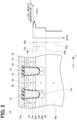
FIG. 2 is an enlarged cross-sectional view of an upper portion of the MOSFET according to the first embodiment. -
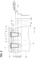
FIG. 3 is an enlarged cross-sectional view of an upper portion of a MOSFET according to a second embodiment. -
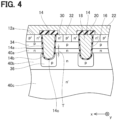
FIG. 4 is an enlarged cross-sectional view of an upper portion of a MOSFET according to a third embodiment. -
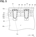
FIG. 5 is an enlarged cross-sectional view of an upper portion of a MOSFET according to a fourth embodiment. -
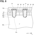
FIG. 6 is an enlarged cross-sectional view of an upper portion of a MOSFET according to a fifth embodiment. - In the above-described field effect transistor, the current spreading n-layer may not be in contact with the gate insulating film at the bottom connection surface.
- According to this configuration, the dielectric breakdown of the gate insulating film can be more effectively suppressed.
- The above-described field effect transistor may further include a bottom p-layer in contact with the gate insulating film at the lower end of the trench.
- According to this configuration, the electric field applied to the gate insulating film around the lower end of the trench can be suppressed.
- In the above-described field effect transistor, the bottom p-layer may be in contact with the current spreading n-layer in a range in contact with the gate insulating film. The current spreading n-layer between the body layer and the bottom p-layer may have a thickness of 0.1 µm or greater.
- According to this configuration, the body layer and the bottom p-layer can be reliably separated by the current spreading n-layer.
- A metal-oxide-semiconductor field effect transistor (MOSFET) 10 shown in
FIGS. 1 and2 has asemiconductor substrate 12, in which an x direction is parallel to theupper surface 12a of thesemiconductor substrate 12, and a y direction is parallel to theupper surface 12a and perpendicular to the x direction. Thesemiconductor substrate 12 is made of SiC. Alternatively, thesemiconductor substrate 12 may be made of another semiconductor such as Si and GaN.Trenches 14 are provided in theupper surface 12a of thesemiconductor substrate 12. Each of thetrenches 14 extends in the y direction on theupper surface 12a. Thetrenches 14 are spaced apart from each other in the x-direction. An inner surface of each of thetrenches 14 is covered with agate insulating film 16. Agate electrode 18 is disposed in each of thetrenches 14. Thegate electrode 18 is insulated from thesemiconductor substrate 12 by thegate insulating film 16. An upper surface of thegate electrode 18 is covered with aninterlayer insulating film 20. Asource electrode 22 is disposed on the upper portion of thesemiconductor substrate 12. Thesource electrode 22 covers theupper surface 12a of thesemiconductor substrate 12 and theinterlayer insulating film 20. Thesource electrode 22 is insulated from thegate electrodes 18 by theinterlayer insulating film 20. Thelower surface 12b of thesemiconductor substrate 12 is covered with adrain electrode 24. - As shown in
FIG. 2 , thetrench 14 has aside surface 14a, abottom connection surface 14b, and abottom surface 14c. Theside surface 14a is a flat surface (more specifically, a surface having a radius of curvature of 0.7 µm or more in the cross-section) that extends in the depth direction (i.e., thickness direction) of thesemiconductor substrate 12. Thebottom surface 14c extends approximately parallel to theupper surface 12a of thesemiconductor substrate 12 and constitutes the lower end of thetrench 14. Thebottom connection surface 14b is a concave curved surface that connects the lower end of theside surface 14a and thebottom surface 14c. In the cross section, the radius of curvature of thebottom connection surface 14b is less than 0.7 µm. - The
semiconductor substrate 12 includes asource layer 30, abody contact layer 32, abody layer 34, a bottom p-layer 36, a connection p-layer 38, and a lower n-layer 40. - The
source layer 30 is an n-type layer, and is in contact with thegate insulating film 16 at the upper end of theside surface 14a of thetrench 14. Thesource layers 30 is in ohmic contact with thesource electrode 22. - The
body contact layer 32 is a p-type layer, and is in ohmic contact with thesource electrode 22 at a position adjacent to thesource layer 30. - The
body layer 34 is a p-type layer having a lower p-type impurity concentration than thebody contact layer 32. Thebody layer 34 contacts thesource layer 30 and thebody contact layer 32 from the lower side. Thebody layer 34 is in contact with thegate insulating films 16 at position below the source layers 30. Thebody layer 34 is in contact with thegate insulating film 16 at theside surface 14a of thetrench 14. - The bottom p-
layer 36 is a p-type layer, and is in contact with thegate insulating film 16 at thebottom surface 14c of thetrench 14. The bottom p-layer 36 extends in the y direction along thebottom surface 14c of thetrench 14. - The connection p-
layer 38 is a p-type layer, and protrudes downward from thebody layer 34. The connection p-layer 38 extends linearly along the x direction when thesemiconductor substrate 12 is viewed from the upper side. The connection p-layer 38 extends in the depth direction to the depth of the bottom p-layer 36. The connection p-layer 38 connects thebody layer 34 and the bottom p-layer 36. - The lower n-
layer 40 is disposed below thebody layer 34. The lower n-layer 40 is separated from thesource layer 30 by thebody layer 34. The lower n-layer 40 is distributed from the position of the lower end of thebody layer 34 to thelower surface 12b of thesemiconductor substrate 12. The lower n-layer 40 includes a current spreading n-layer 40a, an electric field relaxation n-layer 40b, adrift layer 40c, abuffer layer 40d, and adrain layer 40e. - The current spreading n-
layer 40a is an n-type layer having a relatively high concentration of n-type impurities. The current spreading n-layer 40a contacts thebody layer 34 from the lower side. The current spreading n-layer 40a is in contact with thegate insulating film 16 below thebody layer 34. - The electric field relaxation n-
layer 40b is an n-type layer having a lower n-type impurity concentration than the current spreading n-layer 40a. The electric field relaxation n-layer 40b contacts the current spreading n-layer 40a from the lower side. The electric field relaxation n-layer 40b is distributed from the lower end of the current spreading n-layer 40a to a position below the bottom p-layer 36. The electric field relaxation n-layer 40b contacts thegate insulating film 16 below the current spreading n-layer 40a. The electric field relaxation n-layer 40b is in contact with the side surface and the bottom surface of the bottom p-layer 36. - The
drift layer 40c is an n-type layer having a lower n-type impurity concentration than the electric field relaxation n-layer 40b. Thedrift layer 40c is in contact with the electric field relaxation n-layer 40b from the lower side. - The
buffer layer 40d is an n-type layer having a higher n-type impurity concentration than thedrift layer 40c. Thebuffer layer 40d contacts thedrift layer 40c from the lower side. - The
drain layer 40e is an n-type layer having a higher n-type impurity concentration than thebuffer layer 40d. Thedrain layer 40e is in contact with thebuffer layer 40d from the lower side. Thedrain layer 40e is in ohmic contact with thedrain electrode 24. - As shown in
FIG. 2 , in the current spreading n-layer 40a, the n-type impurity concentration is distributed in the depth direction of thesemiconductor substrate 12 in a normal distribution pattern. In the current spreading n-layer 40a, the n-type impurity concentration is distributed in the depth direction of thesemiconductor substrate 12 so as to have a peak value nmax. In other words, the region in which the n-type impurity concentration is normally distributed so as to have the peak value nmax is the current spreading n-layer 40a. In the electric field relaxation n-layer 40b, the n-type impurity concentration is distributed at a substantially constant value that is lower than that in the current spreading n-layer 40a. In thedrift layer 40c, the n-type impurity concentration is distributed at a substantially constant value that is lower than that in the electric field relaxation n-layer 40b. - A portion of the current spreading n-
layer 40a having the peak value nmax is in contact with thegate insulating film 16 on theside surface 14a of the trench 14 (that is, the surface having a radius of curvature of 0.7 µm or more). In the first embodiment, the entire current spreading n-layer 40a is in contact with thegate insulating film 16 on theside surface 14a of thetrench 14. That is, the current spreading n-layer 40a is not in contact with thegate insulating film 16 at thebottom connection surface 14b of thetrench 14. The electric field relaxation n-layer 40b is in contact with thegate insulating film 16 within the range between the current spreading n-layer 40a and the bottom p-layer 36. The electric field relaxation n-layer 40b contacts thegate insulating film 16 at thebottom connection surface 14b. - When the
MOSFET 10 is used, a higher potential is applied to thedrain electrode 24 as compared to thesource electrode 22. The potential of thegate electrode 18 is controlled independently of the potentials of thedrain electrode 24 and thesource electrode 22. When a potential higher than the gate threshold is applied to thegate electrode 18, a channel is formed in thebody layer 34 in a region adjacent to thegate insulating film 16, and the channel connects thesource layer 30 and the current spreading n-layer 40a. As a result, electrons flow from thesource layer 30 through the channel, the current spreading n-layer 40a, the electric field relaxation n-layer 40b, thedrift layer 40c, and thebuffer layer 40d to thedrain layer 40e. This turns on theMOSFET 10. The current spreading n-layer 40a has a relatively high n-type impurity concentration and therefore has a low resistance. Therefore, electrons that have flowed from the channel into the current spreading n-layer 40a tend to flow in the current spreading n-layer 40a along the x-direction. Therefore, in thedrift layer 40c located below the current spreading n-layer 40a, electrons flow toward thedrain layer 40e while being dispersed in the x-direction. In this way, electrons flow in a dispersed manner within thedrift layer 40c, so that theMOSFET 10 has a low on-resistance. - When the potential of the
gate electrode 18 is reduced to a potential below the gate threshold, the channel disappears and the flow of electrons stops. In other words, theMOSFET 10 is turned off. As a result, a depletion layer extends from thebody layer 34 into the current spreading n-layer 40a, the electric field relaxation n-layer 40b, and thedrift layer 40c. The voltage between thedrain electrode 24 and thesource electrode 22 is maintained by the depletion layer that spreads in the current spreading n-layer 40a, the electric field relaxation n-layer 40b, and thedrift layer 40c. Furthermore, when theMOSFET 10 is turned off, a depletion layer extends from the bottom p-layer 36 into the surrounding electric field relaxation n-layer 40b. The depletion layer extending from the bottom p-layer 36 suppresses electric field concentration near the bottom end of thetrench 14. - When the current spreading n-
layer 40a and the electric field relaxation n-layer 40b are depleted, an electric field is applied to thegate insulating film 16. The electric field tends to concentrate in the curved portion of thegate insulating film 16. That is, the electric field is more likely to concentrate on thegate insulating film 16 covering thebottom connection surface 14b than on thegate insulating film 16 covering theside surface 14a. On the other hand, if the density of fixed charges present in the depletion layer in contact with thegate insulating film 16 is high, the electric field applied to thegate insulating film 16 becomes strong. That is, the higher the n-type impurity concentration in the n-type layer in contact with thegate insulating film 16, the stronger the electric field applied to thegate insulating film 16. In this embodiment, the electric field relaxation n-layer 40b with a low n-type impurity concentration is in contact with thegate insulating film 16 at thebottom connection surface 14b where electric field concentration is likely to occur. This restricts an excessively high electric field from being applied to thegate insulating film 16 covering thebottom connection surface 14b, and suppresses dielectric breakdown of thegate insulating film 16 in this portion. Further, the current spreading n-layer 40a having a high n-type impurity concentration is connected to thegate insulating film 16 at theside surface 14a where electric field concentration is unlikely to occur. This restricts an excessively high electric field from being applied to thegate insulating film 16 in the area in contact with the current spreading n-layer 40a, and suppresses dielectric breakdown of thegate insulating film 16 in this area. - As described above, according to the
MOSFET 10 of this embodiment, the on-resistance of theMOSFET 10 can be reduced by the current spreading n-layer 40a while restricting dielectric breakdown of thegate insulating film 16. - In the MOSFET of the second embodiment shown in
FIG. 3 , the thickness of the current spreading n-layer 40a is thicker than that of theMOSFET 10 of the first embodiment. Other configurations of the MOSFET of the second embodiment are the same as those of theMOSFET 10 of the first embodiment. - In the second embodiment, the lower end of the current spreading n-
layer 40a contacts thegate insulating film 16 at thebottom connection surface 14b. However, a portion of the current spreading n-layer 40a having the peak value nmax is in contact with thegate insulating film 16 at theside surface 14a. That is, the portion having the peak value nmax does not contact thegate insulating film 16 at thebottom connection surface 14b, and a portion of the current spreading n-layer 40a with a low n-type impurity concentration contacts thegate insulating film 16 at thebottom connection surface 14b. Therefore, even in this configuration, the electric field applied to the portion of thegate insulating film 16 covering thebottom connection surface 14b can be suppressed. - The bottom p-
layer 36 may be formed by ion implantation of p-type impurities into the bottom of thetrench 14 prior to the formation of thegate electrode 18. In this case, as shown inFIG. 4 , the bottom p-layer 36 may be formed so that the bottom p-layer 36 contacts the current spreading n-layer 40a from the lower side in the area in contact with thegate insulating film 16. In this configuration, the bottom p-layer 36 is in contact with thegate insulating film 16 over the entirebottom connection surface 14b. This configuration also makes it possible to reduce the electric field applied to thegate insulating film 16 covering thebottom connection surface 14b. - In
FIG. 4 , if the thickness T of the current spreading n-layer 40a is too thin, the separation between thebody layer 34 and the bottom p-layer 36 becomes insufficient, and the characteristics of the MOSFET deteriorate. In order to reliably separate thebody layer 34 and the bottom p-layer 36, the thickness T of the current spreading n-layer 40a between thebody layer 34 and the bottom p-layer 36 can be made thicker than the width W of the depletion layer that occurs in the current spreading n-layer 40a when no voltage is applied to the MOSFET. The width W of the depletion layer can be calculated by the following formula.
- In the above formula, ε is a dielectric constant of the
semiconductor substrate 12, Vbi is a built-in potential, q is an elementary charge, and Nd is an n-type impurity concentration of the current spreading n-layer 40a. The built-in potential Vbi can be calculated by the following formula.
- In the above formula, k is the Boltzmann constant, T is the temperature, Na is the p-type impurity concentration of the
body layer 34, and ni is the intrinsic carrier density. - More specifically, when Na=4 x 1017cm-3, Nd=3 x 1017 cm-3 , and ni=1 x 10⁻⁸ cm-3, the thickness T can be set to 0.1 µm or more.
- In the MOSFET of the fourth embodiment shown in
FIG. 5 , the electric field relaxation n-layer 40b does not exist, and thedrift layer 40c contacts the current spreading n-layer 40a from the lower side. Other configurations of the MOSFET of the fourth embodiment are the same as those of theMOSFET 10 of the first embodiment. In the fourth embodiment, thedrift layer 40c having an even lower n-type impurity concentration than the electric field relaxation n-layer 40b contacts thegate insulating film 16 at thebottom connection surface 14b. Therefore, the electric field applied to thegate insulating film 16 covering thebottom connection surface 14b can be more effectively suppressed. - In the MOSFET of the fifth embodiment shown in
FIG. 6 , the bottom p-layer 36 does not exist. In this case, the connection p-layer 38 does not need to be provided. Other configurations of the MOSFET of the fifth embodiment are the same as those of the MOSFET of the fourth embodiment. This configuration also makes it possible to suppress the electric field applied to thegate insulating film 16 covering thebottom connection surface 14b. In the first and second embodiments, the bottom p-layer 36 may not be provided. - The electric field relaxation n-
layer 40b in the first to third embodiments and thedrift layer 40c in the fourth and fifth embodiments are examples of a low-concentration n-layer. - Although the embodiments have been described in detail above, these are merely examples and do not limit the scope of claims. The techniques described in claims include various modifications of the specific examples illustrated above. The technical elements described in the present specification or the drawings exhibit technical usefulness alone or in various combinations, and are not limited to the combinations described in the claims at the time of filing. In addition, the techniques illustrated in the present specification or drawings achieve a plurality of objectives at the same time, and achieving one of the objectives itself has technical usefulness.
Claims (4)
- A field effect transistor comprising:a semiconductor substrate having a trench on an upper surface;a gate insulating film that covers an inner surface of the trench; anda gate electrode disposed inside the trench and insulated from the semiconductor substrate by the gate insulating film, whereinthe semiconductor substrate includes:an n-type source layer in contact with the gate insulating film;a p-type body layer in contact with the gate insulating film below the source layer; anda lower n-layer disposed below the body layer,the lower n-layer includes:a current spreading n-layer in contact with the body layer from a lower side; anda low-concentration n-layer in contact with the current spreading n-layer from a lower side, the low-concentration n-layer having a lower n-type impurity concentration than the current spreading n-layer,an n-type impurity concentration distributed in the current spreading n-layer has a peak value in a depth direction of the semiconductor substrate,the inner surface of the trench has:a side surface having a curvature radius of 0.7 µm or more; anda bottom connection surface to connect the side surface and a lower end of the trench, the bottom connection surface being a concave curved surface having a curvature radius less than 0.7 µm, anda portion of the current spreading n-layer having the peak value is in contact with the gate insulating film at the side surface.
- The field effect transistor according to claim 1, wherein the current spreading n-layer is not in contact with the gate insulating film at the bottom connection surface.
- The field effect transistor according to claim 1 or 2, further comprising a bottom p-layer in contact with the gate insulating film at the lower end of the trench.
- The field effect transistor according to claim 3, whereinthe bottom p-layer is in contact with the current spreading n-layer within a region in contact with the gate insulating film, andthe current spreading n-layer between the body layer and the bottom p-layer has a thickness of 0.1 µm or more.
Applications Claiming Priority (2)
| Application Number | Priority Date | Filing Date | Title |
|---|---|---|---|
| JP2022135237 | 2022-08-26 | ||
| PCT/JP2023/021200 WO2024042814A1 (en) | 2022-08-26 | 2023-06-07 | Field effect transistor |
Publications (2)
| Publication Number | Publication Date |
|---|---|
| EP4579759A1 true EP4579759A1 (en) | 2025-07-02 |
| EP4579759A4 EP4579759A4 (en) | 2025-12-03 |
Family
ID=90012970
Family Applications (1)
| Application Number | Title | Priority Date | Filing Date |
|---|---|---|---|
| EP23856932.1A Pending EP4579759A4 (en) | 2022-08-26 | 2023-06-07 | FIELD EFFECTIVE RANSIST |
Country Status (5)
| Country | Link |
|---|---|
| US (1) | US20250089293A1 (en) |
| EP (1) | EP4579759A4 (en) |
| JP (2) | JP7772236B2 (en) |
| CN (1) | CN119234316A (en) |
| WO (1) | WO2024042814A1 (en) |
Families Citing this family (1)
| Publication number | Priority date | Publication date | Assignee | Title |
|---|---|---|---|---|
| WO2025183962A1 (en) * | 2024-03-01 | 2025-09-04 | Semiconductor Components Industries, Llc | Electronic device including a buried shield and a gap region |
Family Cites Families (11)
| Publication number | Priority date | Publication date | Assignee | Title |
|---|---|---|---|---|
| JP2008016747A (en) * | 2006-07-10 | 2008-01-24 | Fuji Electric Holdings Co Ltd | Trench MOS type silicon carbide semiconductor device and manufacturing method thereof |
| JP4450241B2 (en) | 2007-03-20 | 2010-04-14 | 株式会社デンソー | Method for manufacturing silicon carbide semiconductor device |
| JP5531787B2 (en) * | 2010-05-31 | 2014-06-25 | 株式会社デンソー | Silicon carbide semiconductor device and manufacturing method thereof |
| JP6952826B2 (en) | 2016-10-31 | 2021-10-27 | 株式会社東芝 | Semiconductor devices and their manufacturing methods |
| JP6991476B2 (en) | 2017-05-31 | 2022-01-12 | 国立研究開発法人産業技術総合研究所 | Semiconductor device |
| CN110709997B (en) * | 2017-06-06 | 2023-02-28 | 三菱电机株式会社 | Semiconductor device and power conversion device |
| JP7059556B2 (en) | 2017-10-05 | 2022-04-26 | 富士電機株式会社 | Semiconductor device |
| JP7196463B2 (en) | 2018-08-23 | 2022-12-27 | 富士電機株式会社 | Silicon carbide semiconductor device manufacturing method and silicon carbide semiconductor device |
| US11942538B2 (en) * | 2019-02-04 | 2024-03-26 | Sumitomo Electric Industries, Ltd. | Silicon carbide semiconductor device |
| JP2021034526A (en) | 2019-08-22 | 2021-03-01 | 株式会社デンソー | Manufacturing method of switching element |
| EP4145533A4 (en) | 2020-12-24 | 2024-05-01 | Fuji Electric Co., Ltd. | Insulated gate-type semiconductor device |
-
2023
- 2023-06-07 JP JP2024542598A patent/JP7772236B2/en active Active
- 2023-06-07 EP EP23856932.1A patent/EP4579759A4/en active Pending
- 2023-06-07 WO PCT/JP2023/021200 patent/WO2024042814A1/en not_active Ceased
- 2023-06-07 CN CN202380041413.1A patent/CN119234316A/en active Pending
-
2024
- 2024-11-21 US US18/955,087 patent/US20250089293A1/en active Pending
-
2025
- 2025-09-18 JP JP2025155188A patent/JP2025176181A/en active Pending
Also Published As
| Publication number | Publication date |
|---|---|
| JP2025176181A (en) | 2025-12-03 |
| JP7772236B2 (en) | 2025-11-18 |
| JPWO2024042814A1 (en) | 2024-02-29 |
| US20250089293A1 (en) | 2025-03-13 |
| WO2024042814A1 (en) | 2024-02-29 |
| CN119234316A (en) | 2024-12-31 |
| EP4579759A4 (en) | 2025-12-03 |
Similar Documents
| Publication | Publication Date | Title |
|---|---|---|
| JP7658394B2 (en) | Semiconductor Device | |
| US20230387194A1 (en) | Field effect transistor and method of manufacturing the same | |
| US9214526B2 (en) | Semiconductor device | |
| EP2219224A1 (en) | Semiconductor device | |
| US10468520B2 (en) | Switching element and method of manufacturing the same | |
| US20230037606A1 (en) | Field effect transistor and method of manufacturing the same | |
| WO2016157606A1 (en) | Silicon carbide semiconductor device and method for manufacturing same | |
| US20230395710A1 (en) | Semiconductor device and manufacturing method of semiconductor device | |
| US12369349B2 (en) | Trenched gate double diffused semiconductor device with channel impurity concentration adjustment region | |
| EP4510194A1 (en) | Semiconductor device and method for producing same | |
| US20230369484A1 (en) | Field effect transistor | |
| US20240258425A1 (en) | Semiconductor device and method for manufacturing the same | |
| US20250089293A1 (en) | Field effect transistor | |
| JP7314827B2 (en) | semiconductor equipment | |
| CN117276312A (en) | Silicon carbide power semiconductor device with double shielding structure and manufacturing method thereof | |
| US20200127086A1 (en) | Semiconductor device and method for manufacturing the same | |
| US20240321951A1 (en) | Field effect transistor | |
| US20230361171A1 (en) | Field effect transistor | |
| JP2021129025A (en) | Switching element | |
| CN109119465B (en) | Laterally diffused MOSFET for embedded memory applications | |
| JP7354868B2 (en) | switching element | |
| US20250248065A1 (en) | Semiconductor device and method for manufacturing the same | |
| US20260052741A1 (en) | Mos transistor and method of manufacturing the same | |
| US20250254935A1 (en) | Semiconductor device | |
| US20260090035A1 (en) | Switching element |
Legal Events
| Date | Code | Title | Description |
|---|---|---|---|
| STAA | Information on the status of an ep patent application or granted ep patent |
Free format text: STATUS: THE INTERNATIONAL PUBLICATION HAS BEEN MADE |
|
| PUAI | Public reference made under article 153(3) epc to a published international application that has entered the european phase |
Free format text: ORIGINAL CODE: 0009012 |
|
| STAA | Information on the status of an ep patent application or granted ep patent |
Free format text: STATUS: REQUEST FOR EXAMINATION WAS MADE |
|
| 17P | Request for examination filed |
Effective date: 20241002 |
|
| AK | Designated contracting states |
Kind code of ref document: A1 Designated state(s): AL AT BE BG CH CY CZ DE DK EE ES FI FR GB GR HR HU IE IS IT LI LT LU LV MC ME MK MT NL NO PL PT RO RS SE SI SK SM TR |
|
| REG | Reference to a national code |
Ref country code: DE Ref legal event code: R079 Free format text: PREVIOUS MAIN CLASS: H01L0029780000 Ipc: H10D0030660000 |
|
| STAA | Information on the status of an ep patent application or granted ep patent |
Free format text: STATUS: EXAMINATION IS IN PROGRESS |
|
| A4 | Supplementary search report drawn up and despatched |
Effective date: 20251104 |
|
| DAV | Request for validation of the european patent (deleted) | ||
| DAX | Request for extension of the european patent (deleted) | ||
| RIC1 | Information provided on ipc code assigned before grant |
Ipc: H10D 30/66 20250101AFI20251029BHEP Ipc: H10D 30/60 20250101ALI20251029BHEP Ipc: H10D 62/10 20250101ALI20251029BHEP Ipc: H10D 62/13 20250101ALI20251029BHEP Ipc: H10D 62/17 20250101ALI20251029BHEP Ipc: H10D 62/832 20250101ALI20251029BHEP Ipc: H10D 12/00 20250101ALI20251029BHEP |
|
| 17Q | First examination report despatched |
Effective date: 20251114 |