EP4579753A1 - Quantum device and method for manufacturing quantum device - Google Patents
Quantum device and method for manufacturing quantum device Download PDFInfo
- Publication number
- EP4579753A1 EP4579753A1 EP22956430.7A EP22956430A EP4579753A1 EP 4579753 A1 EP4579753 A1 EP 4579753A1 EP 22956430 A EP22956430 A EP 22956430A EP 4579753 A1 EP4579753 A1 EP 4579753A1
- Authority
- EP
- European Patent Office
- Prior art keywords
- nanopillars
- quantum device
- quantum
- color centers
- electrode pairs
- Prior art date
- Legal status (The legal status is an assumption and is not a legal conclusion. Google has not performed a legal analysis and makes no representation as to the accuracy of the status listed.)
- Pending
Links
Images







Classifications
-
- B—PERFORMING OPERATIONS; TRANSPORTING
- B82—NANOTECHNOLOGY
- B82Y—SPECIFIC USES OR APPLICATIONS OF NANOSTRUCTURES; MEASUREMENT OR ANALYSIS OF NANOSTRUCTURES; MANUFACTURE OR TREATMENT OF NANOSTRUCTURES
- B82Y20/00—Nanooptics, e.g. quantum optics or photonic crystals
-
- H—ELECTRICITY
- H05—ELECTRIC TECHNIQUES NOT OTHERWISE PROVIDED FOR
- H05B—ELECTRIC HEATING; ELECTRIC LIGHT SOURCES NOT OTHERWISE PROVIDED FOR; CIRCUIT ARRANGEMENTS FOR ELECTRIC LIGHT SOURCES, IN GENERAL
- H05B33/00—Electroluminescent light sources
- H05B33/02—Details
- H05B33/06—Electrode terminals
-
- H—ELECTRICITY
- H05—ELECTRIC TECHNIQUES NOT OTHERWISE PROVIDED FOR
- H05B—ELECTRIC HEATING; ELECTRIC LIGHT SOURCES NOT OTHERWISE PROVIDED FOR; CIRCUIT ARRANGEMENTS FOR ELECTRIC LIGHT SOURCES, IN GENERAL
- H05B33/00—Electroluminescent light sources
- H05B33/10—Apparatus or processes specially adapted to the manufacture of electroluminescent light sources
-
- H—ELECTRICITY
- H05—ELECTRIC TECHNIQUES NOT OTHERWISE PROVIDED FOR
- H05B—ELECTRIC HEATING; ELECTRIC LIGHT SOURCES NOT OTHERWISE PROVIDED FOR; CIRCUIT ARRANGEMENTS FOR ELECTRIC LIGHT SOURCES, IN GENERAL
- H05B33/00—Electroluminescent light sources
- H05B33/12—Light sources with substantially two-dimensional [2D] radiating surfaces
- H05B33/14—Light sources with substantially two-dimensional [2D] radiating surfaces characterised by the chemical or physical composition or the arrangement of the electroluminescent material, or by the simultaneous addition of the electroluminescent material in or onto the light source
- H05B33/145—Arrangements of the electroluminescent material
-
- H—ELECTRICITY
- H05—ELECTRIC TECHNIQUES NOT OTHERWISE PROVIDED FOR
- H05B—ELECTRIC HEATING; ELECTRIC LIGHT SOURCES NOT OTHERWISE PROVIDED FOR; CIRCUIT ARRANGEMENTS FOR ELECTRIC LIGHT SOURCES, IN GENERAL
- H05B33/00—Electroluminescent light sources
- H05B33/12—Light sources with substantially two-dimensional [2D] radiating surfaces
- H05B33/18—Light sources with substantially two-dimensional [2D] radiating surfaces characterised by the nature or concentration of the activator
-
- H—ELECTRICITY
- H05—ELECTRIC TECHNIQUES NOT OTHERWISE PROVIDED FOR
- H05B—ELECTRIC HEATING; ELECTRIC LIGHT SOURCES NOT OTHERWISE PROVIDED FOR; CIRCUIT ARRANGEMENTS FOR ELECTRIC LIGHT SOURCES, IN GENERAL
- H05B33/00—Electroluminescent light sources
- H05B33/12—Light sources with substantially two-dimensional [2D] radiating surfaces
- H05B33/20—Light sources with substantially two-dimensional [2D] radiating surfaces characterised by the chemical or physical composition or the arrangement of the material in which the electroluminescent material is embedded
-
- H—ELECTRICITY
- H05—ELECTRIC TECHNIQUES NOT OTHERWISE PROVIDED FOR
- H05B—ELECTRIC HEATING; ELECTRIC LIGHT SOURCES NOT OTHERWISE PROVIDED FOR; CIRCUIT ARRANGEMENTS FOR ELECTRIC LIGHT SOURCES, IN GENERAL
- H05B33/00—Electroluminescent light sources
- H05B33/12—Light sources with substantially two-dimensional [2D] radiating surfaces
- H05B33/26—Light sources with substantially two-dimensional [2D] radiating surfaces characterised by the composition or arrangement of the conductive material used as an electrode
-
- H—ELECTRICITY
- H10—SEMICONDUCTOR DEVICES; ELECTRIC SOLID-STATE DEVICES NOT OTHERWISE PROVIDED FOR
- H10H—INORGANIC LIGHT-EMITTING SEMICONDUCTOR DEVICES HAVING POTENTIAL BARRIERS
- H10H20/00—Individual inorganic light-emitting semiconductor devices having potential barriers, e.g. light-emitting diodes [LED]
- H10H20/80—Constructional details
- H10H20/81—Bodies
- H10H20/811—Bodies having quantum effect structures or superlattices, e.g. tunnel junctions
-
- G—PHYSICS
- G02—OPTICS
- G02F—OPTICAL DEVICES OR ARRANGEMENTS FOR THE CONTROL OF LIGHT BY MODIFICATION OF THE OPTICAL PROPERTIES OF THE MEDIA OF THE ELEMENTS INVOLVED THEREIN; NON-LINEAR OPTICS; FREQUENCY-CHANGING OF LIGHT; OPTICAL LOGIC ELEMENTS; OPTICAL ANALOGUE/DIGITAL CONVERTERS
- G02F1/00—Devices or arrangements for the control of the intensity, colour, phase, polarisation or direction of light arriving from an independent light source, e.g. switching, gating or modulating; Non-linear optics
- G02F1/01—Devices or arrangements for the control of the intensity, colour, phase, polarisation or direction of light arriving from an independent light source, e.g. switching, gating or modulating; Non-linear optics for the control of the intensity, phase, polarisation or colour
-
- G—PHYSICS
- G06—COMPUTING OR CALCULATING; COUNTING
- G06N—COMPUTING ARRANGEMENTS BASED ON SPECIFIC COMPUTATIONAL MODELS
- G06N10/00—Quantum computing, i.e. information processing based on quantum-mechanical phenomena
- G06N10/40—Physical realisations or architectures of quantum processors or components for manipulating qubits, e.g. qubit coupling or qubit control
Definitions
- the present disclosure relates to a quantum device and a method for manufacturing the quantum device.
- quantum computers In recent years, research and development of quantum computers have been energetically advanced. For example, a quantum computer using a level of an electron spin in a color center of diamond as a qubit is known. In such a quantum computer, electron spin information is converted into photon information, and optical reading is performed.
- the quantum computer includes a plurality of qubits.
- emission wavelengths of color centers coincide with each other.
- the emission wavelengths of color centers are different in GHz order in terms of frequency due to a defect, distortion, or the like around the color centers.
- a technique for adjusting the emission wavelength of the color center has been proposed, but it is difficult to place a plurality of qubits with high degree of integration.
- An object of the present disclosure is to provide a quantum device capable of improving the degree of integration of qubits and a method for manufacturing the quantum device.
- a quantum device including: a waveguide that has a first surface, and extends in a first direction parallel to the first surface; a plurality of nanopillars coupled to the first surface and arranged in the first direction; color centers formed in each of the plurality of nanopillars; and electrode pairs provided for each of the color centers, in which each of the plurality of nanopillars is inclined from the first direction, and extends in a second direction inclined from a normal direction of the first surface, and electric fields are applied to the color centers from the electrode pairs.
- the degree of integration of qubits may be improved.
- a plane including the X1-X2 direction and the Y1-Y2 direction is described as an XY plane
- a plane including the Y1-Y2 direction and the Z1-Z2 direction is described as a YZ plane
- a plane including the Z1-Z2 direction and the X1-X2 direction is described as a ZX plane.
- the Z1-Z2 direction is defined as a vertical direction, where a Z1 side is defined as an upper side, and a Z2 side is defined as a lower side.
- a planar view refers to viewing an object from the Z1 side
- a planar shape refers to a shape of an object viewed from the Z1 side.
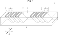
- FIG. 1 is a perspective view illustrating a quantum device according to the first embodiment.
- FIG. 2 is a plan view illustrating the quantum device according to the first embodiment.
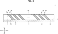
- FIG. 3 is a cross-sectional view illustrating the quantum device according to the first embodiment.
- FIG. 3 corresponds to a cross-sectional view taken along line III-III in FIG. 2 .
- the quantum device 1 mainly includes a slab waveguide 10, a plurality of nanopillars 20, a plurality of electrode pairs 30, and an embedded member 40.
- the slab waveguide 10 extends in the X1-X2 direction.
- the slab waveguide 10 has an upper surface 11 perpendicular to the Z1-Z2 direction.
- the shape of a cross section of the slab waveguide 10 perpendicular to the X1-X2 direction is a rectangular shape.
- the dimension (height) of this cross section in the Z1-Z2 direction is, for example, about 100 nm.
- the refractive index of the slab waveguide 10 is lower than the refractive index of diamond.
- the slab waveguide 10 is made of sapphire, and the upper surface 11 is a c-plane of sapphire.
- the slab waveguide 10 is an example of a waveguide.
- the X1-X2 direction is an example of a first direction.
- the upper surface 11 is an example of a first surface.
- the nanopillar 20 is made of diamond.
- the nanopillar 20 is provided over the upper surface 11 and coupled to the upper surface 11.
- the plurality of nanopillars 20 is arranged in the X1-X2 direction.
- the nanopillar 20 extends in a second direction inclined from the X1-X2 direction.
- the second direction is a direction between the X1-X2 direction and the Z1-Z2 direction, and the nanopillar 20 is inclined toward the X2 side as it goes upward (Z1 side).
- the second direction is parallel to the [111] direction of diamond. When viewed from a direction perpendicular to the upper surface 11, the second direction overlaps the X1-X2 direction.
- An angle ⁇ 1 formed by the upper surface 11 of the slab waveguide 10 and the second direction is 28.5°.
- the nanopillar 20 has an upper surface 22 parallel to the upper surface 11 of the slab waveguide 10.
- the dimension of the upper surface 22 in the X1-X2 direction is about 100 nm
- the dimension of the upper surface 22 in the Y1-Y2 direction is about 200 nm.
- the distance between the upper surface 11 and the upper surface 22 is, for example, about 250 nm to 1000 nm.
- the upper surface 22 is the (110) plane of diamond.
- the shape of a cross section of the nanopillar 20 perpendicular to the second direction is a rectangular shape. This cross section has long sides parallel to the Y1-Y2 direction.
- Each of the plurality of nanopillars 20 includes a color center 21.
- the color center 21 is located in the vicinity of the upper surface 22. For example, the distance from the upper surface 22 to the color center 21 is 100 nm or less.
- the color center 21 is, for example, a nitrogen-vacancy center (NV center) including a nitrogen atom and a vacancy. That is, the color center 21 is a complex defect of nitrogen atoms and vacancies.
- the direction in which nitrogen atoms and vacancies are arranged (hereinafter, will be sometimes referred to as a "defect axis direction") is parallel to the [111] direction of diamond.
- the nanopillars 20 including the color centers 21 can function as qubits.
- the embedded member 40 is provided over the upper surface 11 of the slab waveguide 10 and fills a gap between the plurality of nanopillars 20.
- an upper surface of the embedded member 40 is flush with the upper surfaces 22 of the nanopillars 20.
- the refractive index of the embedded member 40 is lower than the refractive index of diamond.
- the embedded member 40 is made of silicon oxide (SiO 2 ). Side surfaces of the nanopillars 20 are in direct contact with the embedded member 40.
- the nanopillars 20 are surrounded by the embedded member 40.
- the electrode pairs 30 are provided for each of the nanopillars 20.
- the electrode pair 30 includes electrodes 31 and 32.
- the electrodes 31 and 32 are provided over the embedded member 40.
- the color center 21 is located between the electrodes 31 and 32.
- the electrode 31 is located on the X1 side, and the electrode 32 is located on the X2 side.
- the material of the electrodes 31 and 32 is not particularly limited, but is preferably a material having less light absorption in a visible light region that is relevant to a signal wavelength.
- a material of the electrodes 31 and 32 is, for example, gold (Au), silver (Ag), or copper (Cu).
- FIGs. 4 to 11 are cross-sectional views illustrating the method for manufacturing the quantum device 1 according to the first embodiment.
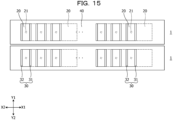
- FIGs. 12 to 15 are plan views illustrating the method for manufacturing the quantum device 1 according to the first embodiment.
- a sapphire substrate 15 and a diamond substrate 25 are prepared, and an upper surface of the sapphire substrate 15 and a lower surface of the diamond substrate 25 are bonded.
- the sizes of the sapphire substrate 15 and the diamond substrate 25 are assumed, for example, to be sizes that allow a plurality of quantum devices 1 to be formed in the Y1-Y2 direction.
- the upper surface of the sapphire substrate 15 is made to have the c-plane
- the upper surface of the diamond substrate 25 is made to have the (110) plane.
- the diamond substrate 25 for example, a high-quality synthetic diamond substrate is used.
- the bonding room-temperature bonding without using a sizing agent, such as surface-activated room-temperature bonding, is desirable.
- the surface-activated room-temperature bonding the upper surface of the sapphire substrate 15 and the lower surface of the diamond substrate 25 are brought into an active state, that is, a state in which dangling bonds are exposed, using argon ions or the like in vacuum, and the upper surface of the sapphire substrate 15 and the lower surface of the diamond substrate 25 are affixed to each other. Bonding using a sizing agent having no absorption band in the visible light region may be performed.
- the sapphire substrate 15 is an example of a first substrate
- the diamond substrate 25 is an example of a second substrate.
- a mask 60 is formed over portions of the upper surface of the diamond substrate 25 intended to constitute the upper surfaces 22 of the nanopillars 20.
- the mask 60 is, for example, a silicon nitride (SiN) film.
- the mask 60 can be formed by, for example, photolithography.
- FIG. 6 corresponds to a cross-sectional view taken along line VI-VI in FIG. 12 .
- the mask 60 is then removed, and the embedded member 40 is formed.
- the embedded member 40 can be formed by, for example, a chemical vapor deposition (CVD) method.
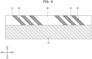
- the color centers 21 are formed in each nanopillar 20.
- ion implantation with nitrogen ions is performed.
- an acceleration voltage is adjusted such that the color center 21 can be formed in the vicinity of the upper surface 22 of the nanopillar 20.
- the dose amount is defined as 10 10 /cm 2 or less.
- several levels of color centers 21 are formed for each of the nanopillars 20.
- an annealing treatment at 1000°C or higher is performed in vacuum or in an inert gas atmosphere.
- the treatment time is desirably set such that the luminescence characteristics of the color centers 21 (luminescence intensity per color center 21) are optimized.
- the sapphire substrate 15 is thinned, and the slab waveguide 10 is formed from the sapphire substrate 15.
- the thickness of the slab waveguide 10 is defined as, for example, about 100 nm.
- FIG. 11 corresponds to a cross-sectional view taken along line XI-XI in FIG. 14 .
- the quantum device 1 according to the first embodiment can be manufactured in this manner.
- the color center 21 may be a silicon-vacancy center (SiV center) including silicon and a vacancy, a germanium-vacancy center (GeV center) including germanium and a vacancy, a tin-vacancy center (SnV center) including tin and a vacancy, a lead-vacancy center (PbV center) including lead and a vacancy, or a boron-vacancy center (BV center) including boron and a vacancy.
- SiV center silicon-vacancy center
- GaV center germanium-vacancy center
- SnV center tin-vacancy center
- PbV center lead-vacancy center
- BV center boron-vacancy center
- direct current (DC) power supplies 35 are individually coupled to each electrode pair 30.
- a negative electrode of the DC power supply 35 is coupled to the electrode 31, and a positive electrode of the DC power supply 35 is coupled to the electrode 32. Therefore, an electric field is applied to the color center 21 from the electrode pair 30.
- This electric field includes a component perpendicular to a defect axis of the color center 21 (hereinafter, will be sometimes referred to as a "perpendicular component").
- the color center 21 is irradiated with a laser beam 26 in the visible light region.
- the wavelength of the laser beam 26 is, for example, 520 nm to 720 nm.
- the color center 21 emits light when irradiated with the laser beam 26. Since the nanopillar 20 is surrounded by the embedded member 40 having a refractive index lower than that of diamond, light generated at the color center 21 is confined in the nanopillar 20. Then, this light propagates through the nanopillar 20 as signal light 27 along the second direction (a direction parallel to the [111] direction of diamond) in which the nanopillar 20 extends. At this time, the signal light 27 propagates through the nanopillar 20 in a single mode only with the transverse electric (TE) mode having an electric field amplitude component only in the direction (Y1-Y2 direction) parallel to the long sides of the cross section of the nanopillar 20 perpendicular to the second direction. That is, the signal light 27 undergoes single-mode propagation through the nanopillar 20 in the second direction.
- TE transverse electric
- the total reflection angle at an interface 50 between the diamond nanopillar 20 and the slab waveguide 10 made of sapphire is 46.8°
- the angle ⁇ 1 formed by the traveling direction of the signal light 27 in the nanopillar 20 and the interface 50 is 28.5°. That is, the angle ⁇ 1 is less than the total reflection angle. Therefore, the signal light 27 propagated to the interface 50 is guided to the slab waveguide 10 from the nanopillar 20 with high efficiency. Furthermore, the signal light 27 guided into the slab waveguide 10 propagates through the slab waveguide 10 while maintaining the single mode of the TE mode.
- the electrode pairs 30 and the wiring are formed over the embedded member 40. Accordingly, compared with a case where the electrode pair 30 or the wiring made of metal is formed over the nanopillar 20, the signal light 27 is easily confined in the nanopillar 20, and the optical loss caused by metal may be reduced.
- FIG. 20 is a diagram illustrating a relationship between a wavelength and transmittance in various metals.
- FIG. 20 illustrates the transmittance of Au, Ag, Cu, and aluminum (Al) films having a thickness of 5 nm calculated using the Drude model. As illustrated in FIG. 20 , a higher transmittance than that of Al can be obtained with Au, Ag, or Cu.
Landscapes
- Engineering & Computer Science (AREA)
- Chemical & Material Sciences (AREA)
- Nanotechnology (AREA)
- Manufacturing & Machinery (AREA)
- Physics & Mathematics (AREA)
- Life Sciences & Earth Sciences (AREA)
- Biophysics (AREA)
- Optics & Photonics (AREA)
- Crystallography & Structural Chemistry (AREA)
- Optical Modulation, Optical Deflection, Nonlinear Optics, Optical Demodulation, Optical Logic Elements (AREA)
Abstract
Description
- The present disclosure relates to a quantum device and a method for manufacturing the quantum device.
- In recent years, research and development of quantum computers have been energetically advanced. For example, a quantum computer using a level of an electron spin in a color center of diamond as a qubit is known. In such a quantum computer, electron spin information is converted into photon information, and optical reading is performed.
-
- Patent Document 1:
U.S. Patent Application Publication No. 2011/0309265 - Patent Document 2:
U.S. Patent Application Publication No. 2012/0161663 - Patent Document 3:
Japanese National Publication of International Patent Application No. 2015-529328 - Patent Document 4:
Japanese National Publication of International Patent Application No. 2007-526639 -
- Non-Patent Document 1: C. T. Nguyen et al., Phys. Rev. Lett. 123, 183602 (2019)
- Non-Patent Document 2: A. Sipahigil et al., Science 354, 847 (2016)
- Non-Patent Document 3: Ph. Tamarat et al., PHYSICAL REVIEW LETTERS 97, 083002 (2006)
- Non-Patent Document 4: L. D. Santis et al., PHYSICAL REVIEW LETTERS 127, 147402 (2021)
- Non-Patent Document 5: J. Lisenfeld, npj Quantum Information (2019), 5: 105
- The quantum computer includes a plurality of qubits. At the time of operation, in order to ensure indistinguishability of photons involved in forming entanglement between the plurality of qubits, it is desirable that emission wavelengths of color centers coincide with each other. However, the emission wavelengths of color centers are different in GHz order in terms of frequency due to a defect, distortion, or the like around the color centers. Conventionally, a technique for adjusting the emission wavelength of the color center has been proposed, but it is difficult to place a plurality of qubits with high degree of integration.
- An object of the present disclosure is to provide a quantum device capable of improving the degree of integration of qubits and a method for manufacturing the quantum device.
- According to an aspect of the present disclosure, there is provided a quantum device including: a waveguide that has a first surface, and extends in a first direction parallel to the first surface; a plurality of nanopillars coupled to the first surface and arranged in the first direction; color centers formed in each of the plurality of nanopillars; and electrode pairs provided for each of the color centers, in which each of the plurality of nanopillars is inclined from the first direction, and extends in a second direction inclined from a normal direction of the first surface, and electric fields are applied to the color centers from the electrode pairs.
- According to the present disclosure, the degree of integration of qubits may be improved.
-
-
FIG. 1 is a perspective view illustrating a quantum device according to a first embodiment. -
FIG. 2 is a plan view illustrating the quantum device according to the first embodiment. -
FIG. 3 is a cross-sectional view illustrating the quantum device according to the first embodiment. -
FIG. 4 is a cross-sectional view (part 1) illustrating a method for manufacturing the quantum device according to the first embodiment. -
FIG. 5 is a cross-sectional view (part 2) illustrating the method for manufacturing the quantum device according to the first embodiment. -
FIG. 6 is a cross-sectional view (part 3) illustrating the method for manufacturing the quantum device according to the first embodiment. -
FIG. 7 is a cross-sectional view (part 4) illustrating the method for manufacturing the quantum device according to the first embodiment. -
FIG. 8 is a cross-sectional view (part 5) illustrating the method for manufacturing the quantum device according to the first embodiment. -
FIG. 9 is a cross-sectional view (part 6) illustrating the method for manufacturing the quantum device according to the first embodiment. -
FIG. 10 is a cross-sectional view (part 7) illustrating the method for manufacturing the quantum device according to the first embodiment. -
FIG. 11 is a cross-sectional view (part 8) illustrating the method for manufacturing the quantum device according to the first embodiment. -
FIG. 12 is a plan view (part 1) illustrating the method for manufacturing the quantum device according to the first embodiment. -
FIG. 13 is a plan view (part 2) illustrating the method for manufacturing the quantum device according to the first embodiment. -
FIG. 14 is a plan view (part 3) illustrating the method for manufacturing the quantum device according to the first embodiment. -
FIG. 15 is a plan view (part 4) illustrating the method for manufacturing the quantum device according to the first embodiment. -
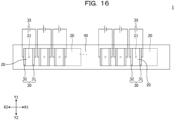
FIG. 16 is a top view illustrating an example of a method for using the quantum device according to the first embodiment. -
FIG. 17 is a cross-sectional view illustrating an example of the method for using the quantum device according to the first embodiment. -
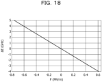
FIG. 18 is a diagram (part 1) illustrating a relationship between an intensity F of an electric field and a change amount ΔE of an optical transition frequency. -
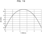
FIG. 19 is a diagram (part 2) illustrating a relationship between the intensity F of the electric field and the change amount ΔE of the optical transition frequency. -
FIG. 20 is a diagram illustrating a relationship between a wavelength and transmittance in various metals. -
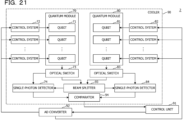
FIG. 21 is a diagram illustrating a quantum operation device according to a second embodiment. - Hereinafter, embodiments of the present disclosure will be specifically described with reference to the accompanying drawings. Note that, in the present description and the drawings, constituent elements having substantially the same functional configuration will be given the same reference sign, and redundant explanation will sometimes not be made. In the present disclosure, it is assumed that an X1-X2 direction, a Y1-Y2 direction, and a Z1-Z2 direction are directions orthogonal to each other. A plane including the X1-X2 direction and the Y1-Y2 direction is described as an XY plane, a plane including the Y1-Y2 direction and the Z1-Z2 direction is described as a YZ plane, and a plane including the Z1-Z2 direction and the X1-X2 direction is described as a ZX plane. Note that, for convenience, the Z1-Z2 direction is defined as a vertical direction, where a Z1 side is defined as an upper side, and a Z2 side is defined as a lower side. In addition, a planar view refers to viewing an object from the Z1 side, and a planar shape refers to a shape of an object viewed from the Z1 side.
- A first embodiment will be described.
FIG. 1 is a perspective view illustrating a quantum device according to the first embodiment.FIG. 2 is a plan view illustrating the quantum device according to the first embodiment.FIG. 3 is a cross-sectional view illustrating the quantum device according to the first embodiment.FIG. 3 corresponds to a cross-sectional view taken along line III-III inFIG. 2 . - The
quantum device 1 according to the first embodiment mainly includes aslab waveguide 10, a plurality ofnanopillars 20, a plurality of electrode pairs 30, and an embeddedmember 40. - The
slab waveguide 10 extends in the X1-X2 direction. Theslab waveguide 10 has anupper surface 11 perpendicular to the Z1-Z2 direction. The shape of a cross section of theslab waveguide 10 perpendicular to the X1-X2 direction is a rectangular shape. The dimension (height) of this cross section in the Z1-Z2 direction is, for example, about 100 nm. The refractive index of theslab waveguide 10 is lower than the refractive index of diamond. For example, theslab waveguide 10 is made of sapphire, and theupper surface 11 is a c-plane of sapphire. Theslab waveguide 10 is an example of a waveguide. The X1-X2 direction is an example of a first direction. Theupper surface 11 is an example of a first surface. - The
nanopillar 20 is made of diamond. Thenanopillar 20 is provided over theupper surface 11 and coupled to theupper surface 11. The plurality ofnanopillars 20 is arranged in the X1-X2 direction. Thenanopillar 20 extends in a second direction inclined from the X1-X2 direction. For example, the second direction is a direction between the X1-X2 direction and the Z1-Z2 direction, and thenanopillar 20 is inclined toward the X2 side as it goes upward (Z1 side). The second direction is parallel to the [111] direction of diamond. When viewed from a direction perpendicular to theupper surface 11, the second direction overlaps the X1-X2 direction. An angle θ1 formed by theupper surface 11 of theslab waveguide 10 and the second direction is 28.5°. Thenanopillar 20 has anupper surface 22 parallel to theupper surface 11 of theslab waveguide 10. For example, the dimension of theupper surface 22 in the X1-X2 direction is about 100 nm, and the dimension of theupper surface 22 in the Y1-Y2 direction is about 200 nm. The distance between theupper surface 11 and theupper surface 22 is, for example, about 250 nm to 1000 nm. Theupper surface 22 is the (110) plane of diamond. The shape of a cross section of thenanopillar 20 perpendicular to the second direction is a rectangular shape. This cross section has long sides parallel to the Y1-Y2 direction. - Each of the plurality of
nanopillars 20 includes acolor center 21. Thecolor center 21 is located in the vicinity of theupper surface 22. For example, the distance from theupper surface 22 to thecolor center 21 is 100 nm or less. Thecolor center 21 is, for example, a nitrogen-vacancy center (NV center) including a nitrogen atom and a vacancy. That is, thecolor center 21 is a complex defect of nitrogen atoms and vacancies. The direction in which nitrogen atoms and vacancies are arranged (hereinafter, will be sometimes referred to as a "defect axis direction") is parallel to the [111] direction of diamond. Thenanopillars 20 including the color centers 21 can function as qubits. - The embedded
member 40 is provided over theupper surface 11 of theslab waveguide 10 and fills a gap between the plurality ofnanopillars 20. For example, an upper surface of the embeddedmember 40 is flush with theupper surfaces 22 of thenanopillars 20. The refractive index of the embeddedmember 40 is lower than the refractive index of diamond. For example, the embeddedmember 40 is made of silicon oxide (SiO2). Side surfaces of thenanopillars 20 are in direct contact with the embeddedmember 40. Thenanopillars 20 are surrounded by the embeddedmember 40. - The electrode pairs 30 are provided for each of the
nanopillars 20. Theelectrode pair 30 includeselectrodes electrodes member 40. In planar view, thecolor center 21 is located between theelectrodes color center 21, theelectrode 31 is located on the X1 side, and theelectrode 32 is located on the X2 side. The material of theelectrodes electrodes - Next, a method for manufacturing the
quantum device 1 according to the first embodiment will be described.FIGs. 4 to 11 are cross-sectional views illustrating the method for manufacturing thequantum device 1 according to the first embodiment.FIGs. 12 to 15 are plan views illustrating the method for manufacturing thequantum device 1 according to the first embodiment. - First, as illustrated in
FIG. 4 , asapphire substrate 15 and adiamond substrate 25 are prepared, and an upper surface of thesapphire substrate 15 and a lower surface of thediamond substrate 25 are bonded. The sizes of thesapphire substrate 15 and thediamond substrate 25 are assumed, for example, to be sizes that allow a plurality ofquantum devices 1 to be formed in the Y1-Y2 direction. For example, the upper surface of thesapphire substrate 15 is made to have the c-plane, and the upper surface of thediamond substrate 25 is made to have the (110) plane. As thediamond substrate 25, for example, a high-quality synthetic diamond substrate is used. As the bonding, room-temperature bonding without using a sizing agent, such as surface-activated room-temperature bonding, is desirable. In the surface-activated room-temperature bonding, the upper surface of thesapphire substrate 15 and the lower surface of thediamond substrate 25 are brought into an active state, that is, a state in which dangling bonds are exposed, using argon ions or the like in vacuum, and the upper surface of thesapphire substrate 15 and the lower surface of thediamond substrate 25 are affixed to each other. Bonding using a sizing agent having no absorption band in the visible light region may be performed. Thesapphire substrate 15 is an example of a first substrate, and thediamond substrate 25 is an example of a second substrate. - The
diamond substrate 25 is then polished to make the thickness of thediamond substrate 25 coincident with the distance between theupper surfaces 22 of thenanopillars 20 and theupper surface 11 of theslab waveguide 10, as illustrated inFIG. 5 . The polishing is, for example, mechanical polishing, chemical mechanical polishing, dry etching, or the like. - Thereafter, as illustrated in
FIGs. 6 and12 , amask 60 is formed over portions of the upper surface of thediamond substrate 25 intended to constitute theupper surfaces 22 of thenanopillars 20. Themask 60 is, for example, a silicon nitride (SiN) film. Themask 60 can be formed by, for example, photolithography.FIG. 6 corresponds to a cross-sectional view taken along line VI-VI inFIG. 12 . - Subsequently, as illustrated in
FIGs. 7 and13 , a plurality ofnanopillars 20 is formed from thediamond substrate 25 by reactive ion etching (RIE) using oxygen (O2)ions 61 incident from a direction parallel to the [111] direction of thediamond substrate 25. In this RIE, for example, the upper surface of thediamond substrate 25 is inclined by 28.5° with respect to the incident direction of the O2 ions 61. Thenanopillars 20 are formed so as to extend parallel to the [111] direction of diamond. By using the SiN film as themask 60, high tolerance can be obtained.FIG. 7 corresponds to a cross-sectional view taken along line VII-VII inFIG. 13 . - As illustrated in
FIG. 8 , themask 60 is then removed, and the embeddedmember 40 is formed. The embeddedmember 40 can be formed by, for example, a chemical vapor deposition (CVD) method. - Thereafter, as illustrated in
FIG. 9 , the color centers 21 are formed in eachnanopillar 20. In a case of forming the NV center, ion implantation with nitrogen ions is performed. At the time of ion implantation, an acceleration voltage is adjusted such that thecolor center 21 can be formed in the vicinity of theupper surface 22 of thenanopillar 20. In addition, for example, the dose amount is defined as 1010/cm2 or less. In this case, several levels of color centers 21 are formed for each of thenanopillars 20. Then, after the ion implantation, an annealing treatment at 1000°C or higher is performed in vacuum or in an inert gas atmosphere. For example, the treatment time is desirably set such that the luminescence characteristics of the color centers 21 (luminescence intensity per color center 21) are optimized. - Subsequently, as illustrated in
FIG. 10 , thesapphire substrate 15 is thinned, and theslab waveguide 10 is formed from thesapphire substrate 15. The thickness of theslab waveguide 10 is defined as, for example, about 100 nm. - As illustrated in
FIGs. 11 and14 , the electrode pairs 30 including theelectrodes nanopillars 20. At this time, wiring (not illustrated) coupled to the electrode pairs 30 is also formed. The electrode pairs 30 and the wiring are formed over the embeddedmember 40.FIG. 11 corresponds to a cross-sectional view taken along line XI-XI inFIG. 14 . - Thereafter, as illustrated in
FIG. 15 , the structure illustrated inFIGs. 11 and14 is divided in the Y1-Y2 direction to obtain a plurality ofquantum devices 1. The division can be performed by, for example, laser ablation or a dry process. - The
quantum device 1 according to the first embodiment can be manufactured in this manner. - Note that the
color center 21 may be a silicon-vacancy center (SiV center) including silicon and a vacancy, a germanium-vacancy center (GeV center) including germanium and a vacancy, a tin-vacancy center (SnV center) including tin and a vacancy, a lead-vacancy center (PbV center) including lead and a vacancy, or a boron-vacancy center (BV center) including boron and a vacancy. - Here, an example of a method for using the
quantum device 1 according to the first embodiment will be described.FIG. 16 is a top view illustrating an example of a method for using thequantum device 1 according to the first embodiment.FIG. 17 is a cross-sectional view illustrating an example of the method for using thequantum device 1 according to the first embodiment. - In this example, as illustrated in
FIG. 16 , direct current (DC) power supplies 35 are individually coupled to eachelectrode pair 30. For example, a negative electrode of theDC power supply 35 is coupled to theelectrode 31, and a positive electrode of theDC power supply 35 is coupled to theelectrode 32. Therefore, an electric field is applied to thecolor center 21 from theelectrode pair 30. This electric field includes a component perpendicular to a defect axis of the color center 21 (hereinafter, will be sometimes referred to as a "perpendicular component"). In addition, as illustrated inFIG. 17 , thecolor center 21 is irradiated with alaser beam 26 in the visible light region. The wavelength of thelaser beam 26 is, for example, 520 nm to 720 nm. - The
color center 21 emits light when irradiated with thelaser beam 26. Since thenanopillar 20 is surrounded by the embeddedmember 40 having a refractive index lower than that of diamond, light generated at thecolor center 21 is confined in thenanopillar 20. Then, this light propagates through thenanopillar 20 assignal light 27 along the second direction (a direction parallel to the [111] direction of diamond) in which thenanopillar 20 extends. At this time, thesignal light 27 propagates through thenanopillar 20 in a single mode only with the transverse electric (TE) mode having an electric field amplitude component only in the direction (Y1-Y2 direction) parallel to the long sides of the cross section of thenanopillar 20 perpendicular to the second direction. That is, thesignal light 27 undergoes single-mode propagation through thenanopillar 20 in the second direction. - In addition, in the present embodiment, the total reflection angle at an
interface 50 between thediamond nanopillar 20 and theslab waveguide 10 made of sapphire is 46.8°, whereas the angle θ1 formed by the traveling direction of thesignal light 27 in thenanopillar 20 and theinterface 50 is 28.5°. That is, the angle θ1 is less than the total reflection angle. Therefore, thesignal light 27 propagated to theinterface 50 is guided to theslab waveguide 10 from thenanopillar 20 with high efficiency. Furthermore, thesignal light 27 guided into theslab waveguide 10 propagates through theslab waveguide 10 while maintaining the single mode of the TE mode. - In addition, the electrode pairs 30 and the wiring are formed over the embedded
member 40. Accordingly, compared with a case where theelectrode pair 30 or the wiring made of metal is formed over thenanopillar 20, thesignal light 27 is easily confined in thenanopillar 20, and the optical loss caused by metal may be reduced. - Here, control for the wavelength of the
signal light 27 will be described. In the present embodiment, the electric field having the perpendicular component can be applied to thecolor center 21. When such an electric field is applied, the optical transition wavelength in thecolor center 21 changes due to the Stark effect. The change amount ΔE in the optical transition frequency is expressed by following formula (1) when the intensity of the perpendicular component of the electric field is assumed as F and the second-order term of F is inclusively considered.
[Mathematical Formula 1] - In
mathematical formula 1, Δµ denotes a change amount of dipole moment between the ground level and the excitation level, Δα denotes a change amount of polarizability tensor between the ground level and the excitation level, and ε denotes the relative permittivity of diamond. - In a case where the
color center 21 is the NV center, there is a relationship illustrated inFIG. 18 between the intensity F of the perpendicular component and the change amount ΔE of the optical transition frequency. Since the NV center has low symmetry in the defect axis direction, Δα has substantially 0 Å3, and ΔE is expressed by a linear formula of F. When using the value of Δµ (4.329 × 10⁻³⁰ C·m) obtained from the description ofNon-Patent Document 3, the result that ΔE could be changed by about 5 GHz by changing the intensity F of the perpendicular component by about 1.0 MV/m was obtained, as illustrated inFIG. 18 . - In a case where the
color center 21 is the SnV center, there is a relationship illustrated inFIG. 19 between the intensity F of the perpendicular component and the change amount ΔE of the optical transition frequency. Since the SnV center has high symmetry in the defect axis direction, ΔE is insensitive to the first-order term of F and is greatly affected by the second-order term of F. When using the value of Δµ ((1.332 × 10⁻²⁴ C·m) and the value of Δα (0.23 Å3) obtained from the description ofNon-Patent Document 4, the result that ΔE could be changed by about 5 GHz by changing the intensity F of the perpendicular component by about 1.0 MV/m was obtained, as illustrated inFIG. 19 . - From these results, it may be said that the optical transition frequency of the
color center 21 can be adjusted in a range of about 5 GHz by applying the electric field using theelectrode pair 30. In other words, it may be said that the emission wavelength in thecolor center 21 can be adjusted. - In addition, in the present embodiment, since the plurality of
nanopillars 20 and theslab waveguide 10 overlap in the Z1-Z2 direction, the degree of integration may be improved, as compared with a configuration in which a qubit and a waveguide are placed in one plane. - For example, it is assumed that the dimension of the
upper surface 22 is 100 nm, the dimensions of theelectrodes upper surfaces 22 is 200 nm in the X1-X2 direction, and the dimension of theupper surface 22 in the Y1-Y2 direction is 200 nm. In this case, in a plane including eachupper surface 22, the dimension of a region for securing two qubits is 460 nm in the X1-X2 direction, the dimension thereof is 200 nm in the Y1-Y2 direction, and the area thereof is 0.092 µm2. Therefore, the occupied area per qubit is 0.046 µm2. On the other hand, the occupied area per qubit of the superconducting quantum computer described inNon-Patent Document 5 is 90,000 µm2. In other words, according to the present embodiment, the occupied area per qubit can be formed smaller by approximately seven digits. - As described above, in the present embodiment, since the
nanopillars 20 partially overlap each other in the Z1-Z2 direction, the interval between thenanopillars 20 in a plane parallel to theupper surface 11 can be narrowed, and the degree of integration of qubits may be improved. - According to the present embodiment, both of adjustment of the emission wavelengths of the color centers 21 and improvement in the degree of integration of qubits may be achieved. By improving the degree of integration, the scale of an optical circuit including the color centers 21 may be increased.
- The
electrodes electrode pair 30 are preferably made of a material having less light absorption in the visible light region.FIG. 20 is a diagram illustrating a relationship between a wavelength and transmittance in various metals.FIG. 20 illustrates the transmittance of Au, Ag, Cu, and aluminum (Al) films having a thickness of 5 nm calculated using the Drude model. As illustrated inFIG. 20 , a higher transmittance than that of Al can be obtained with Au, Ag, or Cu. - Note that the second direction does not have to be parallel to the [111] direction of diamond. The angle θ1 is preferably less than the total reflection angle at the
interface 50. - A second embodiment will be described.
FIG. 21 is a diagram illustrating a quantum operation device according to the second embodiment. Thequantum operation device 2 functions as a quantum computer. - The
quantum operation device 2 according to the second embodiment includesquantum modules control systems optical switches photon detectors quantum operation device 2 further includes a cooler 90, acontrol unit 91, an analog-to-digital (AD)converter 92, abeam splitter 93, and acomparator 94. Thequantum modules control systems optical switches photon detectors AD converter 92, thebeam splitter 93, and thecomparator 94 are housed inside the cooler 90. The temperature inside the cooler 90 is 4 K or less. - The
control unit 91 outputs an analog signal for control to theAD converter 92, theAD converter 92 converts the analog signal into a digital signal, and the digital signal is input to thecontrol systems control unit 91 is, for example, a personal computer. - As the
quantum modules quantum device 1 according to the first embodiment is used. Thequantum module 70 includes a plurality ofqubits 71, and thequantum module 80 includes asmany qubits 81 as thequbits 71. Thequbits nanopillars 20 including the color centers 21 in thequantum device 1. Thecontrol systems 72 are provided for each of thequbits 71, and thecontrol systems 82 are provided for each of thequbits 81. Thecontrol systems 72 each control a magnetic field, an electric field, and a microwave applied to thecorresponding qubit 71 and irradiates thecorresponding qubit 71 with a laser beam. Thecontrol systems 82 each control a magnetic field, an electric field, and a microwave applied to thecorresponding qubit 81 and irradiates thecorresponding qubit 81 with a laser beam. The application of the magnetic field is used to form a state of thecolor center 21 in which the quantum manipulation is performed. The application of the microwave is used to control a state of thecolor center 21. The irradiation of the laser beam is used to read a state of the color center 21 (single photon generation). The application of the electric field is used to control the emission wavelength of thecolor center 21. In the control for the electric field, the electric field is controlled via theelectrode pair 30. - The signal light (photon) generated by the
quantum module 70 is input to theoptical switch 73, and theoptical switch 73 outputs the signal light to the single-photon detector 74 or thebeam splitter 93. In addition, the signal light (photon) generated by thequantum module 80 is input to theoptical switch 83, and theoptical switch 83 outputs the signal light to the single-photon detector 84 or thebeam splitter 93. The signal light input to thebeam splitter 93 is output to the single-photon detectors quantum module 70 is switched by theoptical switch 73 between a path directly guided to the single-photon detector 74 and a path guided to the single-photon detector 74 by way of thebeam splitter 93. Similarly, the path of the signal light generated by thequantum module 80 is switched by theoptical switch 83 between a path directly guided to the single-photon detector 84 and a path guided to the single-photon detector 84 by way of thebeam splitter 93. - For example, at the time of reading a state of a single qubit, the signal light is directly guided to the single-
photon detector quantum module optical switch photon detector quantum module beam splitter 93 by theoptical switch nanopillars 20 having identical optical path lengths from thebeam splitter 93 are used between thequantum modules - The
comparator 94 is used at the time of an entanglement operation and compares detection signals for a single photon after being branched by the beam splitter 93 (which of the single-photon detector comparator 94 corresponds to the result of operation by thequantum operation device 2. - Note that a spectrometer is not used to adjust the emission wavelengths between the
quantum modules - According to the
quantum operation device 2 configured as described above, since thequantum device 1 according to the first embodiment is used for thequantum modules quantum operation device 2 with high reliability may be obtained. - Although the preferred embodiments and the like have been described in detail so far, the embodiments are not restricted to the above-described embodiments and the like, and various modifications and substitutions can be made to the embodiments and the like described above, without departing from the scope disclosed in the claims.
-
- 1: quantum device
- 2: quantum operation device
- 10: slab waveguide
- 11: upper surface
- 15: sapphire substrate
- 20: nanopillar
- 21: color center
- 22: upper surface
- 25: diamond substrate
- 30: electrode pair
- 31, 32: electrodes
- 40: embedded member
- 50: interface
Claims (13)
- A quantum device comprising:a waveguide that has a first surface, and extends in a first direction parallel to the first surface;a plurality of nanopillars coupled to the first surface and arranged in the first direction;color centers formed in each of the plurality of nanopillars; andelectrode pairs provided for each of the color centers, whereineach of the plurality of nanopillars is inclined from the first direction, and extends in a second direction inclined from a normal direction of the first surface, andelectric fields are applied to the color centers from the electrode pairs.
- The quantum device according to claim 1, comprising an embedded member that is provided over the first surface, and fills a gap between the plurality of nanopillars.
- The quantum device according to claim 2, wherein a material of the nanopillars is diamond, and a refractive index of the embedded member is lower than the refractive index of the diamond.
- The quantum device according to claim 2 or 3, wherein the electrode pairs are provided over the embedded member.
- The quantum device according to claim 1 or 2, wherein a material of the nanopillars is diamond, and a refractive index of the waveguide is lower than the refractive index of the diamond.
- The quantum device according to claim 1 or 2, wherein the first direction and the second direction overlap when the first surface is viewed from the normal direction.
- The quantum device according to claim 1 or 2, wherein an angle formed by the first surface and the second direction is less than a total reflection angle at an interface between the waveguide and the nanopillars.
- The quantum device according to claim 1 or 2, wherein the electric fields include a component perpendicular to a direction in which atoms and vacancies that constitute the color centers are arranged.
- The quantum device according to claim 1 or 2, whereina shape of a cross section of the nanopillars perpendicular to the second direction is a rectangular shape, andlight that propagates through the nanopillars undergoes a single-mode propagation in the second direction.
- The quantum device according to claim 9, wherein the light that propagates through the nanopillars has an electric field amplitude component only in a direction parallel to a long side of the cross section.
- The quantum device according to claim 1 or 2, wherein the color centers include a complex defect of nitrogen (N), silicon (Si), germanium (Ge), tin (Sn), or lead (Pb), or any combination of the N, Si, Ge, Sn, or Pb, and vacancies.
- The quantum device according to claim 1 or 2, wherein the electrode pairs contain gold (Au), silver (Ag), or copper (Cu).
- A method for manufacturing a quantum device, comprising:a process of bonding a second substrate that has a refractive index higher than the refractive index of a first substrate, to a first surface of the first substrate;a process of processing the second substrate to form a plurality of nanopillars arranged in a first direction parallel to the first surface;a process of forming color centers in each of the plurality of nanopillars; anda process of forming electrode pairs for each of the color centers, whereineach of the plurality of nanopillars is inclined from the first direction, and extends in a second direction inclined from a normal direction of the first surface, andelectric fields are applied to the color centers from the electrode pairs.
Applications Claiming Priority (1)
| Application Number | Priority Date | Filing Date | Title |
|---|---|---|---|
| PCT/JP2022/031682 WO2024042602A1 (en) | 2022-08-23 | 2022-08-23 | Quantum device and method for manufacturing quantum device |
Publications (2)
| Publication Number | Publication Date |
|---|---|
| EP4579753A1 true EP4579753A1 (en) | 2025-07-02 |
| EP4579753A4 EP4579753A4 (en) | 2025-10-15 |
Family
ID=90012729
Family Applications (1)
| Application Number | Title | Priority Date | Filing Date |
|---|---|---|---|
| EP22956430.7A Pending EP4579753A4 (en) | 2022-08-23 | 2022-08-23 | QUANTUM DEVICE AND METHOD FOR MANUFACTURING QUANTUM DEVICE |
Country Status (4)
| Country | Link |
|---|---|
| US (1) | US20250185129A1 (en) |
| EP (1) | EP4579753A4 (en) |
| JP (1) | JPWO2024042602A1 (en) |
| WO (1) | WO2024042602A1 (en) |
Family Cites Families (8)
| Publication number | Priority date | Publication date | Assignee | Title |
|---|---|---|---|---|
| US20070277730A1 (en) * | 2004-03-02 | 2007-12-06 | James Rabeau | Photon Source |
| US9082673B2 (en) * | 2009-10-05 | 2015-07-14 | Zena Technologies, Inc. | Passivated upstanding nanostructures and methods of making the same |
| US20100148221A1 (en) * | 2008-11-13 | 2010-06-17 | Zena Technologies, Inc. | Vertical photogate (vpg) pixel structure with nanowires |
| AU2010275863A1 (en) | 2009-07-23 | 2012-02-09 | Commissariat A L'energie Atomique | An electrically driven single photon source |
| US8415640B2 (en) | 2010-04-19 | 2013-04-09 | President And Fellows Of Harvard College | Diamond nanowires |
| WO2014051886A1 (en) * | 2012-08-22 | 2014-04-03 | President And Fellows Of Harvard College | Nanoscale scanning sensors |
| KR102318555B1 (en) * | 2020-03-19 | 2021-10-29 | 한국과학기술연구원 | Inverted nano-cone structure for photonic device and the method for manufacturing the same |
| CN116235091A (en) * | 2020-12-01 | 2023-06-06 | 富士通株式会社 | Quantum circuit, quantum computer and method of manufacturing quantum circuit |
-
2022
- 2022-08-23 WO PCT/JP2022/031682 patent/WO2024042602A1/en not_active Ceased
- 2022-08-23 JP JP2024542470A patent/JPWO2024042602A1/ja active Pending
- 2022-08-23 EP EP22956430.7A patent/EP4579753A4/en active Pending
-
2025
- 2025-01-29 US US19/040,672 patent/US20250185129A1/en active Pending
Also Published As
| Publication number | Publication date |
|---|---|
| US20250185129A1 (en) | 2025-06-05 |
| JPWO2024042602A1 (en) | 2024-02-29 |
| EP4579753A4 (en) | 2025-10-15 |
| WO2024042602A1 (en) | 2024-02-29 |
Similar Documents
| Publication | Publication Date | Title |
|---|---|---|
| Schwartz et al. | Fully on-chip single-photon Hanbury-Brown and Twiss experiment on a monolithic semiconductor–superconductor platform | |
| Hollenbach et al. | Engineering telecom single-photon emitters in silicon for scalable quantum photonics | |
| JP2928532B2 (en) | Quantum interference optical device | |
| Li et al. | Resolving single plasmons generated by multiquantum-emitters on a silver nanowire | |
| Fischer et al. | On-chip infrared photonics with Si-Ge-heterostructures: What is next? | |
| Cady et al. | Diamond optomechanical crystals with embedded nitrogen-vacancy centers | |
| Große et al. | Development of site-controlled quantum dot arrays acting as scalable sources of indistinguishable photons | |
| Abb et al. | Interference, coupling, and nonlinear control of high-order modes in single asymmetric nanoantennas | |
| Holewa et al. | Droplet epitaxy symmetric InAs/InP quantum dots for quantum emission in the third telecom window: morphology, optical and electronic properties | |
| Song et al. | Efficient excitation of multiple plasmonic modes on three-dimensional graphene: an unexplored dimension | |
| Kang et al. | Rainbow radiating single-crystal Ag nanowire nanoantenna | |
| Wang et al. | A review of gallium phosphide nanophotonics towards omnipotent nonlinear devices | |
| Assadillayev et al. | Plasmon launching and scattering by silicon nanoparticles | |
| Davoodi et al. | Plasmon–exciton interactions in nanometer-thick gold-WSe2 multilayer structures: implications for photodetectors, sensors, and light-emitting devices | |
| Zheng et al. | Chirped circular dielectric gratings for near-unity collection efficiency from quantum emitters in bulk diamond | |
| Han et al. | On-chip detection of radiation guided by dielectric-loaded plasmonic waveguides | |
| Zheng et al. | Active control of excitonic strong coupling and electroluminescence in electrically driven plasmonic nanocavities | |
| Zhu et al. | Excitonic resonant emission–absorption of surface plasmons in transition metal dichalcogenides for chip-level electronic–photonic integrated circuits | |
| Shi et al. | Probing excitonic rydberg states by plasmon enhanced nonlinear optical spectroscopy in monolayer WS2 at room temperature | |
| TWI840365B (en) | Systems, devices, articles and methods including luminescent local defects in semiconductors with local information states | |
| US20250185129A1 (en) | Quantum device and method for manufacturing quantum device | |
| Glassner et al. | Tuning electroluminescence from a plasmonic cavity-coupled silicon light source | |
| Flaschmann et al. | Optimizing the growth conditions of Al mirrors for superconducting nanowire single-photon detectors | |
| Wang et al. | Cavity-Quantum Electrodynamics with Moir\'e Flatband Photonic Crystals | |
| US20250060530A1 (en) | Thin film lithium niobate hybrid photonics packaging |
Legal Events
| Date | Code | Title | Description |
|---|---|---|---|
| STAA | Information on the status of an ep patent application or granted ep patent |
Free format text: STATUS: THE INTERNATIONAL PUBLICATION HAS BEEN MADE |
|
| PUAI | Public reference made under article 153(3) epc to a published international application that has entered the european phase |
Free format text: ORIGINAL CODE: 0009012 |
|
| STAA | Information on the status of an ep patent application or granted ep patent |
Free format text: STATUS: REQUEST FOR EXAMINATION WAS MADE |
|
| 17P | Request for examination filed |
Effective date: 20250129 |
|
| AK | Designated contracting states |
Kind code of ref document: A1 Designated state(s): AL AT BE BG CH CY CZ DE DK EE ES FI FR GB GR HR HU IE IS IT LI LT LU LV MC MK MT NL NO PL PT RO RS SE SI SK SM TR |
|
| REG | Reference to a national code |
Ref country code: DE Ref legal event code: R079 Free format text: PREVIOUS MAIN CLASS: H01L0029060000 Ipc: B82Y0020000000 |
|
| A4 | Supplementary search report drawn up and despatched |
Effective date: 20250912 |
|
| RIC1 | Information provided on ipc code assigned before grant |
Ipc: B82Y 20/00 20110101AFI20250908BHEP Ipc: H05B 33/06 20060101ALI20250908BHEP Ipc: H05B 33/10 20060101ALI20250908BHEP Ipc: H05B 33/14 20060101ALI20250908BHEP Ipc: H05B 33/18 20060101ALI20250908BHEP Ipc: H05B 33/20 20060101ALI20250908BHEP Ipc: H05B 33/26 20060101ALI20250908BHEP Ipc: H10D 62/10 20250101ALI20250908BHEP Ipc: H10H 20/811 20250101ALI20250908BHEP Ipc: G06N 10/40 20220101ALN20250908BHEP Ipc: G02F 1/01 20060101ALN20250908BHEP |
|
| DAV | Request for validation of the european patent (deleted) | ||
| DAX | Request for extension of the european patent (deleted) |