EP4579215A1 - Chip-integrated luminescence detection for chemical, biological or biochemical sensing - Google Patents
Chip-integrated luminescence detection for chemical, biological or biochemical sensing Download PDFInfo
- Publication number
- EP4579215A1 EP4579215A1 EP24173101.7A EP24173101A EP4579215A1 EP 4579215 A1 EP4579215 A1 EP 4579215A1 EP 24173101 A EP24173101 A EP 24173101A EP 4579215 A1 EP4579215 A1 EP 4579215A1
- Authority
- EP
- European Patent Office
- Prior art keywords
- layer
- sensor chip
- sensed
- particles
- photodiode
- Prior art date
- Legal status (The legal status is an assumption and is not a legal conclusion. Google has not performed a legal analysis and makes no representation as to the accuracy of the status listed.)
- Granted
Links
Images



Classifications
-
- G—PHYSICS
- G01—MEASURING; TESTING
- G01N—INVESTIGATING OR ANALYSING MATERIALS BY DETERMINING THEIR CHEMICAL OR PHYSICAL PROPERTIES
- G01N21/00—Investigating or analysing materials by the use of optical means, i.e. using sub-millimetre waves, infrared, visible or ultraviolet light
- G01N21/75—Systems in which material is subjected to a chemical reaction, the progress or the result of the reaction being investigated
- G01N21/77—Systems in which material is subjected to a chemical reaction, the progress or the result of the reaction being investigated by observing the effect on a chemical indicator
- G01N21/7703—Systems in which material is subjected to a chemical reaction, the progress or the result of the reaction being investigated by observing the effect on a chemical indicator using reagent-clad optical fibres or optical waveguides
-
- G—PHYSICS
- G01—MEASURING; TESTING
- G01N—INVESTIGATING OR ANALYSING MATERIALS BY DETERMINING THEIR CHEMICAL OR PHYSICAL PROPERTIES
- G01N15/00—Investigating characteristics of particles; Investigating permeability, pore-volume or surface-area of porous materials
- G01N15/10—Investigating individual particles
- G01N15/14—Optical investigation techniques, e.g. flow cytometry
- G01N15/1484—Optical investigation techniques, e.g. flow cytometry microstructural devices
-
- G—PHYSICS
- G01—MEASURING; TESTING
- G01N—INVESTIGATING OR ANALYSING MATERIALS BY DETERMINING THEIR CHEMICAL OR PHYSICAL PROPERTIES
- G01N21/00—Investigating or analysing materials by the use of optical means, i.e. using sub-millimetre waves, infrared, visible or ultraviolet light
- G01N21/75—Systems in which material is subjected to a chemical reaction, the progress or the result of the reaction being investigated
- G01N2021/757—Systems in which material is subjected to a chemical reaction, the progress or the result of the reaction being investigated using immobilised reagents
-
- G—PHYSICS
- G01—MEASURING; TESTING
- G01N—INVESTIGATING OR ANALYSING MATERIALS BY DETERMINING THEIR CHEMICAL OR PHYSICAL PROPERTIES
- G01N21/00—Investigating or analysing materials by the use of optical means, i.e. using sub-millimetre waves, infrared, visible or ultraviolet light
- G01N21/75—Systems in which material is subjected to a chemical reaction, the progress or the result of the reaction being investigated
- G01N21/77—Systems in which material is subjected to a chemical reaction, the progress or the result of the reaction being investigated by observing the effect on a chemical indicator
- G01N2021/7769—Measurement method of reaction-produced change in sensor
- G01N2021/7786—Fluorescence
-
- G—PHYSICS
- G01—MEASURING; TESTING
- G01N—INVESTIGATING OR ANALYSING MATERIALS BY DETERMINING THEIR CHEMICAL OR PHYSICAL PROPERTIES
- G01N21/00—Investigating or analysing materials by the use of optical means, i.e. using sub-millimetre waves, infrared, visible or ultraviolet light
- G01N21/62—Systems in which the material investigated is excited whereby it emits light or causes a change in wavelength of the incident light
- G01N21/63—Systems in which the material investigated is excited whereby it emits light or causes a change in wavelength of the incident light optically excited
- G01N21/64—Fluorescence; Phosphorescence
- G01N21/645—Specially adapted constructive features of fluorimeters
- G01N21/648—Specially adapted constructive features of fluorimeters using evanescent coupling or surface plasmon coupling for the excitation of fluorescence
-
- G—PHYSICS
- G01—MEASURING; TESTING
- G01N—INVESTIGATING OR ANALYSING MATERIALS BY DETERMINING THEIR CHEMICAL OR PHYSICAL PROPERTIES
- G01N21/00—Investigating or analysing materials by the use of optical means, i.e. using sub-millimetre waves, infrared, visible or ultraviolet light
- G01N21/75—Systems in which material is subjected to a chemical reaction, the progress or the result of the reaction being investigated
- G01N21/77—Systems in which material is subjected to a chemical reaction, the progress or the result of the reaction being investigated by observing the effect on a chemical indicator
- G01N21/7703—Systems in which material is subjected to a chemical reaction, the progress or the result of the reaction being investigated by observing the effect on a chemical indicator using reagent-clad optical fibres or optical waveguides
- G01N21/7746—Systems in which material is subjected to a chemical reaction, the progress or the result of the reaction being investigated by observing the effect on a chemical indicator using reagent-clad optical fibres or optical waveguides the waveguide coupled to a cavity resonator
Definitions
- the present invention is concerned with a sensor chip for detecting a presence of chemical, biochemical or biological particles to be sensed in an analyte fluid.
- Chip-integrated photonic sensor are typically composed of either interferometers or resonators, realized in a silicon-based photonic integrated circuit (PIC).
- PIC silicon-based photonic integrated circuit
- a PIC can be compared to an electronic integrated circuit. However, it uses photons instead of electrons to transport information.
- PICs employ components like optical waveguides and gratings to guide, separate, polarize, modulate, couple, and, ultimately, to generate and detect light.
- Photonic chip-integrated sensors are generally resistant to electromagnetic interference, exhibit a high sensitivity and a low detection limit, while providing a small footprint, and allow labeled as well as label-free sensing, and also multiplexing of several analytes at the same time. Furthermore, an integration into lab-on-a-chip systems is feasible.
- the LFA test strips consist of a sample pad, a conjugate release pad, a nitrocellulose membrane, and an absorbent pad attached onto a backing card.
- the CIS contains a 256 ⁇ 128 lock-in pixel (LIP) sensor array.
- Each pixel has a size of 10 ⁇ m ⁇ 10 ⁇ m and includes a photodiode acting as signal transducer.
- the LIP architecture blocks interfering light when fluorophores are excited and accumulates the emitted luminescence light to be measured over multiple cycles after excitation based of the intensity difference over time of fluorescence and luminescence.
- a sensor chip for detecting a presence of biochemical or biological particles to be sensed in an analyte fluid comprises
- the photodiode is sensitive to detect, upon capture of one or more of the particles to be sensed by the capturing agent, characteristic light emission or a characteristic change in light emission from the surface functionalization layer in response to supplied excitation energy.
- the emitted characteristic light has a wavelength that is indicative of the presence of the particle to be sensed, and the photodiode is configured to provide a photodiode output signal indicative thereof.
- the present invention provides a sensor chip that allows implementing chemical, biochemical and biological particle sensing applications, which combine ease of use with a particularly high detection sensitivity.
- the sensor chip of the present invention is particularly suited for affordable, high-volume, rapid test applications like water analysis, environmental monitoring, and or food diagnostics.
- the test can be performed directly at the point-of-need, providing a rapid or even real-time measurement result.
- Examples of application cases include the detection of bacteria, viruses and proteins in liquid analyte fluids such as water, urine or blood. However, these fluids are given only for the sake of examples. Other analyte fluids may be used.
- the sensor chip also allows using a gaseous analyte fluid.
- the term fluid is used in the present application as a generic term to cover liquid as well as gaseous analytes.
- Biochemical particles include for instance carbohydrates, lipids, proteins, and nucleic acids.
- Biological particles include microorganisms such as bacteria or virus.
- the sensor chip of the present invention is compatible with industry-standard CMOS processing technologies. As such, it is scalable and particularly suited for low-cost mass production. Also, the sensor application can easily be co-integrated on chip with electronic evaluation and output circuitry.
- the sensor chip has at least one cavity extending from the back side through the base layer and through the buried oxide layer of its SOI substrate, thus exposing a back surface of the silicon layer. It is this exposed back surface, where the sensor chip monolithically integrates a lateral photodiode with a lateral layer sequence of active photodiode layers.
- This lateral layer sequence of active photodiode layers thus forms an integral part of the exposed back surface and as such defines a photosensor surface with a functionalized coating that can be exposed to an analyte fluid comprising particles to be sensed.
- characteristic light that forms a desired signal allowing a detection and identification of the particles to be sensed is generated in closest proximity to the active photodiode layers of the lateral photodiode. This achieves a particularly high sensitivity of the sensor chip in performing its sensing application.
- the functionalized coating has at least one surface functionalization layer provided on the photosensor surface formed by the lateral photodiode.
- the surface functionalization layer on the photosensor surface may comprise a capturing agent.
- a suitable capturing agent is to be selected depending on the particular sensing application case and is thus to be selected with a view to the particles to be sensed.
- the surface functionalization layer may comprise one or more of the following: binder molecules; binder antibodies; fragments of antibodies, for example Fab, Fab2, or scFv fragments; Immunglobulin-G (IgG); a molecularly imprinted polymer (MIP); a peptide; DNA; an aptamere; and/or an affinity protein, such as Protein A, Protein G, Avidin or any of its derivates.
- binder molecules binder antibodies
- fragments of antibodies for example Fab, Fab2, or scFv fragments
- IgG Immunglobulin-G
- MIP molecularly imprinted polymer
- a peptide DNA
- an aptamere and/or an affinity protein, such as Protein A, Protein G, Avidin or any of its derivates.
- the surface functionalization layer is initially provided without the capturing agent, but configured to immobilize the capturing agent upon exposure of the surface functionalization layer to it.
- the material of the functionalization layer is suitably selected for enabling an immobilization of the capturing agent upon exposure to it.
- the sensing solution of the present invention involving a detection of a characteristic light emission can be combined with other known forms of particle detection using other optical sensors such as interferometers or resonators, which can be realized on the same chip in a photonic integrated circuit (PIC).
- PIC photonic integrated circuit
- additional detectors may even be implemented in the same cavity. This way, complementary information can be gathered from the same analyte sample.
- An SOI wafer with pre-fabricated light emitter structures made for instance of III-V nitrides may be provided as an intermediate product for further processing, and suitably covered during the CMOS processing of the sensor chip in order to avoid contamination of the FEOL processing line with undesired chemical elements.
- the sensor chip may further comprise a sealing substrate attached to the SOI substrate on its back side.
- the sealing substrate serves to protect the cavity from exposure to external chemical, electrical or optical impacts.
- the sealing substrate may for instance be made of a metallic, ceramic, or polymeric material, or of a fiber-polymer composite material.
- a particular example is a single-layer circuit board or a multilayer circuit board as used for carrying and electrically connecting chips in integrated circuit packages.
- the second photonic sensor element may be configured to expose the optical input wave to particles to be sensed and captured by the functionalized coating on the active surface element, and to provide the resulting optical output wave with phase information indicative of an interaction between the optical input wave and the captured particles to be sensed;
- a weak perturbation to the evanescent field leads to a change of the effective refractive index and, consequently, to a change of the resonance condition.
- Particles to be senses that are bound on by the functionalized coating the surface induce a resonance shift.
- the sensing information i.e. the resonance shift, can be quantitatively interrogated by measuring either the resonance peak shift or the intensity change at a certain wavelength. This approach can achieve a label-free detection of particles to be sensed.
- the sensor chip 100 has a silicon-on-insulator (SOI) substrate 102, that has a front side F and a back side B and that comprises a silicon layer 103 comprising the front side F and a buried oxide layer 104.
- a base layer 106 (also referred to as “substrate”) comprises the back side B, and a substrate silicon layer 108 is arranged between the silicon layer 103 and the base layer 106.
- An interconnect stack 110 is provided on top of the silicon layer 103 and the buried oxide layer 104. Electrical contacts 112 are provided to the sides on the base layer 106 and are connected to metal structures 114 on a top metal layer of the interconnect stack 110 by wire bonds 116.
- a cavity 118 extends from the back side B through the substrate 106, through the silicon layer 108 and through the buried oxide layer 104 and exposes a back surface BS of the silicon layer 103.
- the base layer 106 covers the cavity 118, but leaves openings 120, 122 for the conduction of fluid into and out of the cavity, as indicated by arrow 123.
- a monolithically integrated lateral photodiode 124 comprises a lateral layer sequence of active photodiode layers, which lateral layer sequence forms an integral part of the exposed back surface BS and as such defines a photosensor surface.
- a functionalized coating (not visible in Fig. 1 ) that has at least one surface functionalization layer on the photosensor surface PS and either comprises a capturing agent or is configured to immobilize a capturing agent upon exposure of the surface functionalization layer to the capturing agent, for selectively capturing the particles to be sensed from an analyte fluid upon exposure of the functionalization layer to the analyte fluid.
- the design of the functionalized coating will be discussed below in the context of the description of Figs. 9 to 12 .
- Fig. 2 is a schematic cross sectional view of another embodiment of a sensor chip 200 for chip-integrated luminescence detection for chemical, biological or biochemical sensing.
- the sensor chip 200 is generally similar to the sensor chip 100 shown in Fig. 1 , with the following difference.
- the sensor chip 200 has a substrate 206 with an excitation window region 226 that is transparent in the lateral region of the cavity 218, i.e. has an excitation window region 226 in the substrate 206. This allows providing excitation light 228 to the surface functionalized layer from an external light source 230, as shown.
- the material of the excitation window region 226 covers the cavity 218 and is transparent for the excitation light.
- the excitation window region 226 has openings 220, 222 for the conduction of fluid into and out of the cavity, as indicated by arrow 223. Otherwise, as mentioned, the sensor chip 200 is similar to that of Fig. 1 .
- Fig. 3 is a schematic cross sectional view of another embodiment of a sensor chip 300 for chip-integrated luminescence detection for chemical, biological or biochemical sensing.
- the sensor chip 200 is generally similar to the sensor chips 100 and 200 shown in Figs. 1 and 2 , respectively, with the following difference.
- the sensor chip 300 has a substrate 306 that is transparent for the excitation light 328, for allowing transmission of excitation light from an external light source 330 to the surface functionalized layer, similarly as in the example of Fig. 2 . However, in the present case it is the full substrate 306, which is transparent, and not only an excitation window region. Otherwise, as mentioned, the sensor chip 300 is also similar to those of Figs. 1 and 2 .
- Fig. 4 is a schematic cross sectional view of another embodiment of a sensor chip 400 for chip-integrated luminescence detection for chemical, biological or biochemical sensing with a substrate 406 that is solid and opaque for the excitation light 428.
- a light source 430 is integrated into the substrate for providing excitation light 428 to the functionalized photosensor surface from across the cavity 418. Otherwise the sensor chip 400 is similar to the sensor chip 100 of Fig. 1 .
- Fig. 5 is an enlarged cross sectional view of an area of a sensor chip 500 comprising a cavity 518 in accordance with another embodiment of the present invention.
- a monolithically integrated lateral photodiode 524 which is typically fabricated in a front-end-of-line processing phase, i.e., before the cavity is fabricated, comprises a lateral n + -p + -layer sequence of active photodiode layers 524.n and 524p, which lateral layer sequence forms an integral part of the exposed back surface BS and as such defines a photosensor surface.
- Exemplary ranges of suitable doping levels of the n + -p + -layer sequence are1 ⁇ 10 16 cm -3 to 1 ⁇ 10 18 cm -3 for a silicon n + layer 524.n and 5 ⁇ 10 18 cm -3 for a silicon p + layer of the lateral photodiode 524.
- Particularly high doping levels for instance in the range of 1x 10 20 cm -3 , are provided in a silicon n ++ contact region 524.nc in the n + layer 524.n and in a silicon p ++ contact region 524.pc in the p + layer 524.p.
- the contact regions 524.nc and 524.pc are contacted using respective conductive vias 540 and 542 extending vertically through the silicon layer 504 of the SOI substrate 502. Laterally, the integral lateral photodiode 524 is embedded between insulating material regions 544 and 546 fabricated as parts of a in a photonic plane 548 in front-end-of line processing.
- Fig. 5 does not show the substrate layer below the buried oxide layer 508 of the SOI substrate 502.
- the underlying substrate layer can be designed according to any of the embodiments described in the context of the embodiments of Figs. 1 to 4 .
- the embodiment of Fig. 5 can also be seen as an enlarged view of the sensor chips 100,200,300, and 400.
- FIG. 6 is an enlarged cross sectional view of an area of another sensor chip 600 comprising a cavity 618 in accordance with another embodiment of the present invention.
- a monolithically integrated lateral photodiode 624 comprises a lateral n + -i-p + -layer sequence of active photodiode layers 624n. 624.i, and 624p, respectively, which lateral layer sequence forms an integral part of the exposed back surface BS and as such defines a photosensor surface, which is laterally embedded between insulating material regions 644 and 646 in a photonic plane 648.
- the present embodiment uses a p-i-n diode 624 as the lateral photodiode, with an additional intrinsically conductive layer 624.i between the p + - and n + -doped layers 624.p and 624.n.
- exemplary ranges of suitable doping levels of the p + - and n + -doped layers 624.p and 624.n of the n + -i-p + -layer sequence are as discussed with reference to the embodiment of Fig. 5 .
- particularly high doping levels are provided in the n ++ contact region 624.nc and the p ++ contact region 624.pc.
- Fig. 7 is an enlarged cross sectional view of an area of a sensor chip 700 comprising a cavity 718 in accordance with another embodiment of the present invention.
- the sensor chip 700 resembles the sensor chip 500 of Fig. 5 , but has a laterally larger cavity 718 which additionally comprises a straight waveguide 750 arranged in a photonic plane of silicon 748, for guiding an optical input wave to the active-surface element and for guiding an optical output wave from the active-surface element to a photonic detector (not shown), which is configured to generate an output signal in response to receiving the optical output wave.
- An example of a second photonic sensor element is a silicon photonic micro-ring resonator (MRR). Reference is made to the functional description in a previous section of this specification.
- the waveguide 750 comprises a core 750.c of an insulating material such as SiO 2 , which is embedded between lateral rails 750.r made of silicon, which may be n-doped.
- the cavity 718 has a lateral extension that also exposes that part of the insulating material region 746, in which the optical waveguide 750 is embedded. This part of the insulating material region 746 on back surface BS in the cavity 718 is also covered with the functionalized coating (not shown).
- an optical input wave is guided to the functional coating (not shown) on the back surface BS of the cavity 718.
- the optical input wave when exposed to particles to be sensed, which have been captured by the functionalized coating on the active surface element, turns into a resulting optical output wave that carries phase information indicative of an interaction between the optical input wave and the captured particles to be sensed.
- the photonic detector is configured to extract the phase information from the optical output wave and to provide a photonic detector output signal indicative of the presence of captured particles to be sensed.
- Fig. 8 is a schematic cross sectional view of an embodiment of a sensor chip assembly 800 for chip-Integrated luminescence detection for chemical, biological or biochemical sensing.
- the sensor chip assembly 800 has a sealing substrate 800.s that is opaque for the excitation light, except in the region of an optical window 860 that is transparent for the excitation light.
- the sealing substrate 800.s is a printed circuit board (PCB) as used in the semiconductor industry in semiconductor device packages.
- a sensor chip 800.c similar to that shown in Fig. 1 is mounted by the bulk silicon (708) on the sealing substrate 800.s. In contrast to the embodiment of Fig. 1 , the substrate layer (106, cf. Fig. 1 ) may be completely removed from the sensor chip 800.c.
- the sensor chip 800.c is mounted on the sealing substrate 800.s using an underfill 800.u.
- An inlet plug 852 with an inlet opening 856 and an outlet plug 854 with an outlet opening 858 are mounted in the substrate 800.s to allow controlling the flow of fluid to the cavity.
- a suitable diameter of the inlet and outlet openings is in the range between 200 and 500 ⁇ m, and in one example amounts to 360 ⁇ m.
- a protective bioinert coating 859 may be used to cover the sealing substrate and protect the sample solution from direct exposure to the substrate.
- the coating may be made of copper, or gold, or made of copper with an electroless Ni / Pd / Au plating (ENEPIG).
- Figs 9 to 11 show an exemplary assay with the hybrid sensor.
- a cross-section of the sensor chip 900, 1000 within the cavity is shown.
- the photonic plane 960, 1060 bellow a back end of line 904, 1004 with waveguides 924, 1024 and a photodiode or avalanche photo diode 926, 1026 is pictured.
- the surface of the photonic plane 960,1060 is coated with covalent attached binders 962, 1062 like fragments of antibodies, for example Fab, Fab2, or scFvfragments; Immunglobulin-G (IgG); a molecularly imprinted polymer (MIP); a peptide; DNA; an aptamere; and/or an affinity protein, such as Protein A, Protein G, Avidin or any of its derivates.
- binders 962, 1062 like fragments of antibodies, for example Fab, Fab2, or scFvfragments
- IgG Immunglobulin-G
- MIP molecularly imprinted polymer
- a peptide DNA
- an aptamere and/or an affinity protein, such as Protein A, Protein G, Avidin or any of its derivates.
- binder antibodies The binder antibodies of the surface functionalization layer are selected to allow capturing the particles that are to be sensed.
- a second step of a possible assay is shown where an analyte L, e.g. a virus, is captured by the antibodies 1062 which are coated on the optical waveguides 1024 and the lateral photo or avalanche diode 1026 on the back end of line 1004.
- An initial shift in the refractive index due to the immobilization of the analyte L is detected by the photonic waveguide structures (indicated as an increase in detected light intensity I MRR in Fig 12 , during the phase II).
- a third step of a possible assay is shown were a labelled detection particle V is added.
- the detection particle consists of a binder label combination e.g., antibody coated quantum nanodots, Eu 3+ -Chelate labelled antibodies or enzyme-antibody conjugates.
- the binders on the detection particles V also bind the analyte L),but must not be identical to the binders 962 used in the example of Fig. 9 . Due to the additional binding of the detection particles V an additional shift of the local refractive index of the photonic sensor structures can be detected (cf. Fig. 12 , phase III). As the label of the detection particle V has light emitting feature properties an additional signal is recorded by the photo diode ( Fig. 12 , phase III, I APD).
Landscapes
- Chemical & Material Sciences (AREA)
- Physics & Mathematics (AREA)
- General Health & Medical Sciences (AREA)
- Health & Medical Sciences (AREA)
- Life Sciences & Earth Sciences (AREA)
- Analytical Chemistry (AREA)
- Biochemistry (AREA)
- General Physics & Mathematics (AREA)
- Immunology (AREA)
- Pathology (AREA)
- Chemical Kinetics & Catalysis (AREA)
- Plasma & Fusion (AREA)
- Engineering & Computer Science (AREA)
- Dispersion Chemistry (AREA)
- Investigating, Analyzing Materials By Fluorescence Or Luminescence (AREA)
Abstract
Description
- The present invention is concerned with a sensor chip for detecting a presence of chemical, biochemical or biological particles to be sensed in an analyte fluid.
- Chip-integrated photonic sensors are considered to have potential for a multitude of biochemical and biological sensing applications such as food analysis, virus detection, healthcare and environmental monitoring.
- Chip-integrated photonic sensor are typically composed of either interferometers or resonators, realized in a silicon-based photonic integrated circuit (PIC). A PIC can be compared to an electronic integrated circuit. However, it uses photons instead of electrons to transport information. As opposed to electronic integrated circuits, which are typically constructed of transistor arrays, PICs employ components like optical waveguides and gratings to guide, separate, polarize, modulate, couple, and, ultimately, to generate and detect light.
- Photonic chip-integrated sensors are generally resistant to electromagnetic interference, exhibit a high sensitivity and a low detection limit, while providing a small footprint, and allow labeled as well as label-free sensing, and also multiplexing of several analytes at the same time. Furthermore, an integration into lab-on-a-chip systems is feasible.
- The publication Alexander Hofmann et al.: Lock-In Pixel CMOS Image Sensor for Time-Resolved Fluorescence Readout of Lateral-Flow Assays; IEEE TRANSACTIONS ON BIOMEDICAL CIRCUITS AND SYSTEMS, VOL. 16, NO. 4, AUGUST 2022; describes a CMOS image sensor (CIS) based implemented in 0.18 µm CMOS technology that performs time-resolved fluorescence (TRF) measurements for filter-less readout of lateral-flow assay (LFA) test strips. The LFA test strips consist of a sample pad, a conjugate release pad, a nitrocellulose membrane, and an absorbent pad attached onto a backing card. The CIS contains a 256 × 128 lock-in pixel (LIP) sensor array. Each pixel has a size of 10 µm × 10 µm and includes a photodiode acting as signal transducer. To detect even small amounts of fluorescence light over a wide analyte concentration range, the LIP architecture blocks interfering light when fluorophores are excited and accumulates the emitted luminescence light to be measured over multiple cycles after excitation based of the intensity difference over time of fluorescence and luminescence.
- According to a first aspect of the present invention, a sensor chip for detecting a presence of biochemical or biological particles to be sensed in an analyte fluid comprises
- a silicon-on-insulator substrate, herein SOI substrate, that has a front side and a back side and that comprises a silicon layer forming the front side, a base layer forming the back side and a buried oxide layer between the silicon layer and the base layer;
- at least one cavity extending from the back side through the base layer and through the buried oxide layer and exposing a back surface of the silicon layer;
- at least one monolithically integrated lateral photodiode that comprises a lateral layer sequence of active photodiode layers, which lateral layer sequence forms an integral part of the exposed back surface and as such defines a photosensor surface; and
- a functionalized coating that has at least one surface functionalization layer on the photosensor surface and either comprises a capturing agent or is configured to immobilize a capturing agent upon exposure of the surface functionalization layer to the capturing agent, for selectively capturing the particles to be sensed from an analyte fluid upon exposure of the functionalization layer to the analyte fluid.
- The photodiode is sensitive to detect, upon capture of one or more of the particles to be sensed by the capturing agent, characteristic light emission or a characteristic change in light emission from the surface functionalization layer in response to supplied excitation energy. The emitted characteristic light has a wavelength that is indicative of the presence of the particle to be sensed, and the photodiode is configured to provide a photodiode output signal indicative thereof.
- The present invention provides a sensor chip that allows implementing chemical, biochemical and biological particle sensing applications, which combine ease of use with a particularly high detection sensitivity. As such, the sensor chip of the present invention is particularly suited for affordable, high-volume, rapid test applications like water analysis, environmental monitoring, and or food diagnostics. The test can be performed directly at the point-of-need, providing a rapid or even real-time measurement result.
- Examples of application cases include the detection of bacteria, viruses and proteins in liquid analyte fluids such as water, urine or blood. However, these fluids are given only for the sake of examples. Other analyte fluids may be used. The sensor chip also allows using a gaseous analyte fluid. Thus, the term fluid is used in the present application as a generic term to cover liquid as well as gaseous analytes.
- The present specification uses the term "biochemical or biological particle" for portions of matter, in particular molecules, that participate in chemical processes within living organisms. Biochemical particles include for instance carbohydrates, lipids, proteins, and nucleic acids. Biological particles include microorganisms such as bacteria or virus.
- The sensor chip of the present invention is compatible with industry-standard CMOS processing technologies. As such, it is scalable and particularly suited for low-cost mass production. Also, the sensor application can easily be co-integrated on chip with electronic evaluation and output circuitry.
- The sensor chip has at least one cavity extending from the back side through the base layer and through the buried oxide layer of its SOI substrate, thus exposing a back surface of the silicon layer. It is this exposed back surface, where the sensor chip monolithically integrates a lateral photodiode with a lateral layer sequence of active photodiode layers. This lateral layer sequence of active photodiode layers thus forms an integral part of the exposed back surface and as such defines a photosensor surface with a functionalized coating that can be exposed to an analyte fluid comprising particles to be sensed. Thus, characteristic light that forms a desired signal allowing a detection and identification of the particles to be sensed is generated in closest proximity to the active photodiode layers of the lateral photodiode. This achieves a particularly high sensitivity of the sensor chip in performing its sensing application.
- The functionalized coating has at least one surface functionalization layer provided on the photosensor surface formed by the lateral photodiode. The surface functionalization layer on the photosensor surface may comprise a capturing agent. A suitable capturing agent is to be selected depending on the particular sensing application case and is thus to be selected with a view to the particles to be sensed. For the sake of providing examples, the surface functionalization layer may comprise one or more of the following: binder molecules; binder antibodies; fragments of antibodies, for example Fab, Fab2, or scFv fragments; Immunglobulin-G (IgG); a molecularly imprinted polymer (MIP); a peptide; DNA; an aptamere; and/or an affinity protein, such as Protein A, Protein G, Avidin or any of its derivates.
- In an alternative embodiment, the surface functionalization layer is initially provided without the capturing agent, but configured to immobilize the capturing agent upon exposure of the surface functionalization layer to it. The material of the functionalization layer is suitably selected for enabling an immobilization of the capturing agent upon exposure to it.
- Notably, the present invention does not impose a specific sensitivity requirement on the photodiode. The above description of the photodiode is not to be understood as necessarily enabling the detection of characteristic light from only a single captured particle to be sensed. While this is desirable and may be achieved in embodiments employing a suitable type photodiode under suitable operating conditions, different embodiments disclosed further below have different photodiodes with different levels of sensitivity. Different types of photodiode have different detection thresholds for emitted characteristic light, which among other factors depends on the spectral sensitivity, operating parameters and noise characteristics of the photodiode under the given operating parameters, and on the wavelength and intensity of the characteristic light per particle to be sensed, and may also depend on optical background noise in a given application environment. A suitable detection sensitivity is to be selected based on a consideration of these parameters and in view of the needs of a particular sensing application case of the sensor chip.
- As will be explained in the context of the description of embodiments of the sensor chip, the sensing solution of the present invention involving a detection of a characteristic light emission can be combined with other known forms of particle detection using other optical sensors such as interferometers or resonators, which can be realized on the same chip in a photonic integrated circuit (PIC). Such additional detectors may even be implemented in the same cavity. This way, complementary information can be gathered from the same analyte sample.
- The following description thus turns to embodiments that include additional features for further improving the sensor chip in different aspects.
- The photodiode of the sensor chip can be implemented in different ways. In one embodiment, the lateral layer sequence of active photodiode layer is a P-N layer sequence. To achieve a larger area for light absorption and thus an improved quantum efficiency of photo detection, a P-I-N layer sequence may be used. Here, P denotes a p-doped semiconductor layer, N denotes an n-doped semiconductor layer, and I denotes an intrinsically conductive semiconductor layer, for instance silicon or silicon-germanium. In an embodiment the photodiode is an avalanche photodiode (APD) or a lateral single-photon APD, which due to their built-in gain mechanism have a particularly high sensitivity for low-level signals of the characteristic light emission
- The material of the photodiode is selected with a view of the wavelength (in other words, energy or frequency) of the characteristic light used for the detection of the particles to be sensed. The photodiode may be sensitive to detect the characteristic light that is emitted directly by the particles to be sensed. Silicon as a photodetector material has a broad spectral range of sensitivity in the near UV, visible spectral range and near infrared. It is generally sensitive in the spectral range between 200 nm and 1100 nm, with the highest sensitivity being in the wavelength range higher than 400 nm. As such, silicon is suited for a broad range of application cases. A shift of the sensitivity to even higher wavelengths in the near infrared may be achieved by using a silicon germanium alloy.
- In an alternative (or in addition to the above) a more indirect method of particle sensing may be used in that (additional) characteristic light is detected that is emitted by label particles such as label molecules. The concept of label particles is per se known. They are also referred to as reporter particles. Label particles have specific chemical properties that can be used to achieve a physical or chemical bond of the label particles only to the particles that are to be sensed and that are captured at the surface functionalization layer. In this regard, it does not matter whether the particles to be detected have bonded to the label molecules before or after getting immobilized on the surface functionalization layer. Furthermore, label particles exhibit a particularly strong emission of characteristic light in response to suitable excitation, such as chemical or optical excitation, making their emission easier to detect than the light emission of many types of particles to be sensed.
- A suitable label particle for a given sensing application is to be selected with a view to achieving a chemical match to the properties of a given particle to be sensed in the sensing application. Furthermore, given a selected label particle, the excitation energy used for the detection mechanism must be selected to match energy absorption characteristics of the label particle such that the absorbed excitation energy is effective in generating the desired characteristic light emission.
- Exemplary label particles are oxidative enzymes that produce the characteristic light in the form of bioluminescence in response to chemical excitation. This applies in particular to the class of luciferases. The peak emission wavelength for luciferases varies depending on the type of luciferase and the substrate used. For example, the peak emission wavelength for firefly luciferase is 560nm. However, other luciferases have emission spectra covering other areas of the electromagnetic spectrum. For instance, the luciferase known under the tradename NanoLuc® has a peak emission wavelength at 460 nm.
- Finally, returning to the properties of the photodiode in this discussion, the material of the photodiode is to be selected to (also) match the emission spectrum of characteristic light emitted by the selected label particle in its bonded state with the particle to be sensed.
- Label particles may also serve for improving detectability of direct characteristic light emitted by the particles to be sensed, in that the label particles may absorb the energy of the direct light and emit their own characteristic light in a wavelength range that meets a higher detector sensitivity. Thus, undetectable direct light emission may serve as a source of excitation energy for the emission of characteristic light to be detected. This may hold true for a shift to higher wavelength by fluorescence or phosphorescence or by a shift from higher to lower wavelengths by up-conversion.
- Different forms of excitation energy may be used for generating the characteristic light emission from the surface functionalization layer or the liquid in the LBE formed cavity in operation of the sensor chip, as described in the following.
- In some embodiments, chemical processes in the functionalized coating provide the required excitation energy. This is for instance the case in the case of NanoLuc® luciferase as a label molecule with the addition of a chemiluminescence agent such as Furimazine.
- In other embodiments, electrogenerated chemiluminescence may be used, wherein the required electrical energy may be provided via suitable electrode structures on chip.
- In further embodiments, the sensor chip may further comprise a monolithically integrated excitation light emitter arranged to emit excitation light for providing the excitation energy to generate the characteristic light emission from the surface functionalization layer carrying the particles to be sensed. The light emitter may be integrated on the SOI substrate. Techniques for integrating light emitters in the visible and near infrared are per se known, even if an integration of light emitters in the visible spectrum with a high processing yield is still a challenging task, in particular if CMOS-compatible processing is a requirement, and may at present result in undesirably high processing cost. However, with further progress in processing technology, such disadvantages are likely to be overcome. An SOI wafer with pre-fabricated light emitter structures made for instance of III-V nitrides may be provided as an intermediate product for further processing, and suitably covered during the CMOS processing of the sensor chip in order to avoid contamination of the FEOL processing line with undesired chemical elements.
- In an alternative embodiment, the sensor chip comprises a monolithically integrated waveguide structure that is arranged and configured to receive excitation light from an external excitation light emitter and to guide the excitation light towards the surface functionalization layer.
- The sensor chip may further comprise a sealing substrate attached to the SOI substrate on its back side. The sealing substrate serves to protect the cavity from exposure to external chemical, electrical or optical impacts. The sealing substrate may for instance be made of a metallic, ceramic, or polymeric material, or of a fiber-polymer composite material. A particular example is a single-layer circuit board or a multilayer circuit board as used for carrying and electrically connecting chips in integrated circuit packages.
- The sealing substrate preferably has a fluid access port that is in fluidic connection with the cavity through the sealing substrate, to allow supplying the analyte fluid to the cavity through the fluid access port and the sealing substrate. Microfluidic Channels may be formed to guide the analyte to the functionalized coating in the cavity, and for guiding any other fluids required for suitable preparation of the functionalized coating. The microfluidic channels may in particular extend along an interface between the SOI substrate and the sealing substrate.
- In some embodiments that use an external light emitter for providing the excitation energy, the sealing substrate comprises the excitation light emitter for providing the excitation light to the surface functionalization layer through the sealing substrate. Since the sealing substrate may be applied to the SOI substrate after CMOS front-end processing, the integration of a light emitter on the sealing substrate can be implemented at a lower processing cost as an integration on the SOI chip.
- In some variants, the sealing substrate may be made of a material that is transparent for the excitation light. This allows particularly simple ways of providing the excitation light to the surface functionalized layer. In some sub-variants, only sections of the sealing substrate are made of such a transparent material, for instance in the form of an integrated excitation window of a material that covers the cavity and is transparent for the excitation light. In other variants, the sealing substrate is made of a material that is opaque for the excitation light. Here, the sealing substrate suitably comprises an optical input port for receiving the excitation light supplied by an external light source that is external to the sensor chip. In all mentioned variants, the sealing substrate may comprise a light propagation structure such as a waveguide allowing propagation of the excitation light to the surface functionalization layer.
- Further embodiments comprise the photodiode in addition to a second photonic sensor element. This allows increasing a dynamic range of the measurement, and in particular the reliability and accuracy of the measurement of the analyte fluid. A second photonic sensor element may for instance include
- an active-surface element arranged on the exposed back surface of the silicon layer in the cavity and having the functionalized coating; and
- a waveguide arranged in a photonic plane for guiding an optical input wave to the active-surface element and for guiding an optical output wave from the active-surface element to a photonic detector, which is configured to generate an output signal in response to receiving the optical output wave.
- The second photonic sensor element may be configured to expose the optical input wave to particles to be sensed and captured by the functionalized coating on the active surface element, and to provide the resulting optical output wave with phase information indicative of an interaction between the optical input wave and the captured particles to be sensed; wherein
- the photonic detector is configured to extract the phase information from the optical output wave and to provide a photonic detector output signal indicative of the presence of captured particles to be sensed.
- An example of a second photonic sensor element is a silicon photonic micro-ring resonator (MRR). Light coupled to the MRR from a straight waveguide via evanescence field coupling. The light is then circulating inside the ring if the resonance condition is fulfilled. In this case, resonance peaks appear in the optical spectrum if the wavelength of the light matches a whole number of times inside the optical length of the ring. The resonance condition is sensitive to changes in the effective refractive index of the ring. The evanescence field, which represents a portion of light that is penetrating inside the surrounding material of the functionalization coating, can interact with the analyte fluid. Thus, a weak perturbation to the evanescent field leads to a change of the effective refractive index and, consequently, to a change of the resonance condition. Particles to be senses that are bound on by the functionalized coating the surface induce a resonance shift. The sensing information, i.e. the resonance shift, can be quantitatively interrogated by measuring either the resonance peak shift or the intensity change at a certain wavelength. This approach can achieve a label-free detection of particles to be sensed.
- According to a second aspect of the present invention, a method for operating a sensor chip according to the first aspect of the invention or one of its embodiments is provided. The method comprises:
- providing a sensor chip according to the first aspect of the invention or one of its embodiments;
- exposing the surface functionalization layer of the sensor chip that comprises immobilized binder molecules to an analyte fluid comprising particles to be sensed;
- supplying excitation energy to the functionalization layer;
- detecting characteristic light emitted from the surface functionalization layer in response to the supplied excitation energy, wherein the characteristic light has a wavelength that is indicative of the presence of the particle to be sensed.
- The method of the second aspect shares the advantages of the sensor chip of the first aspect of the present invention. In the following, further embodiments of the invention will be described with reference to the enclosed drawings. In the drawings:
In the following, further embodiments will be described with reference to the drawings. -
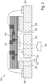
Fig. 1 is a schematic cross sectional view of an embodiment of a sensor chip for chip-Integrated luminescence detection for chemical, biological or biochemical sensing; -
Fig. 2 is a schematic cross sectional view of another embodiment of a sensor chip for chip-Integrated luminescence detection for chemical, biological or biochemical sensing with a substrate that is transparent in the lateral region of the cavity; -
Fig. 3 is a schematic cross sectional view of another embodiment of a sensor chip for chip-Integrated luminescence detection for chemical, biological or biochemical sensing with a substrate that is transparent for the excitation light; -
Fig. 4 is a schematic cross sectional view of another embodiment of a sensor chip with a PCB-integrated light source; -
Fig. 5 is an enlarged cross sectional view of an area of a sensor chip comprising a cavity in accordance with another embodiment of the present invention; -
Fig. 6 is an enlarged cross sectional view of an area of a sensor chip comprising a cavity in accordance with another embodiment of the present invention; -
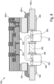
Fig. 7 is an enlarged cross sectional view of an area of a sensor chip comprising a cavity in accordance with another embodiment of the present invention; -
Fig. 8 is a schematic cross sectional view of another embodiment of a sensor chip for chip-Integrated luminescence detection for chemical, biological or biochemical sensing where the sensor chip is mounted on a printed circuit board (PCB); and -
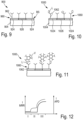
Figs. 9 to 12 are illustrations of a functionalized surface of the photodetector used for particle sensing with characteristic light emitted by label particles and expected sensor signals. -
Fig. 1 is a schematic cross sectional view of an embodiment of asensor chip 100 for chip-integrated luminescence detection for chemical, biological or biochemical sensing. - The
sensor chip 100 has a silicon-on-insulator (SOI)substrate 102, that has a front side F and a back side B and that comprises asilicon layer 103 comprising the front side F and a buriedoxide layer 104. A base layer 106 (also referred to as "substrate") comprises the back side B, and asubstrate silicon layer 108 is arranged between thesilicon layer 103 and thebase layer 106. Aninterconnect stack 110 is provided on top of thesilicon layer 103 and the buriedoxide layer 104.Electrical contacts 112 are provided to the sides on thebase layer 106 and are connected tometal structures 114 on a top metal layer of theinterconnect stack 110 bywire bonds 116. - A
cavity 118 extends from the back side B through thesubstrate 106, through thesilicon layer 108 and through the buriedoxide layer 104 and exposes a back surface BS of thesilicon layer 103. Thebase layer 106 covers thecavity 118, but leavesopenings arrow 123. - A monolithically integrated
lateral photodiode 124 comprises a lateral layer sequence of active photodiode layers, which lateral layer sequence forms an integral part of the exposed back surface BS and as such defines a photosensor surface. - A functionalized coating (not visible in
Fig. 1 ) that has at least one surface functionalization layer on the photosensor surface PS and either comprises a capturing agent or is configured to immobilize a capturing agent upon exposure of the surface functionalization layer to the capturing agent, for selectively capturing the particles to be sensed from an analyte fluid upon exposure of the functionalization layer to the analyte fluid. The design of the functionalized coating will be discussed below in the context of the description ofFigs. 9 to 12 . -
Fig. 2 is a schematic cross sectional view of another embodiment of asensor chip 200 for chip-integrated luminescence detection for chemical, biological or biochemical sensing. Thesensor chip 200 is generally similar to thesensor chip 100 shown inFig. 1 , with the following difference. Thesensor chip 200 has asubstrate 206 with anexcitation window region 226 that is transparent in the lateral region of thecavity 218, i.e. has anexcitation window region 226 in thesubstrate 206. This allows providingexcitation light 228 to the surface functionalized layer from an externallight source 230, as shown. The material of theexcitation window region 226 covers thecavity 218 and is transparent for the excitation light. Theexcitation window region 226 hasopenings arrow 223. Otherwise, as mentioned, thesensor chip 200 is similar to that ofFig. 1 . -
Fig. 3 is a schematic cross sectional view of another embodiment of asensor chip 300 for chip-integrated luminescence detection for chemical, biological or biochemical sensing. Thesensor chip 200 is generally similar to thesensor chips Figs. 1 and2 , respectively, with the following difference. Thesensor chip 300 has asubstrate 306 that is transparent for theexcitation light 328, for allowing transmission of excitation light from an externallight source 330 to the surface functionalized layer, similarly as in the example ofFig. 2 . However, in the present case it is thefull substrate 306, which is transparent, and not only an excitation window region. Otherwise, as mentioned, thesensor chip 300 is also similar to those ofFigs. 1 and2 . -
Fig. 4 is a schematic cross sectional view of another embodiment of asensor chip 400 for chip-integrated luminescence detection for chemical, biological or biochemical sensing with asubstrate 406 that is solid and opaque for theexcitation light 428. Alight source 430 is integrated into the substrate for providingexcitation light 428 to the functionalized photosensor surface from across thecavity 418. Otherwise thesensor chip 400 is similar to thesensor chip 100 ofFig. 1 . -
Fig. 5 is an enlarged cross sectional view of an area of asensor chip 500 comprising acavity 518 in accordance with another embodiment of the present invention. A monolithically integratedlateral photodiode 524, which is typically fabricated in a front-end-of-line processing phase, i.e., before the cavity is fabricated, comprises a lateral n+-p+-layer sequence of active photodiode layers 524.n and 524p, which lateral layer sequence forms an integral part of the exposed back surface BS and as such defines a photosensor surface. Exemplary ranges of suitable doping levels of the n+-p+-layer sequence are1×1016 cm-3 to 1×1018 cm-3 for a silicon n+ layer 524.n and 5×1018 cm-3 for a silicon p+ layer of thelateral photodiode 524. Particularly high doping levels, for instance in the range of 1x 1020 cm-3, are provided in a silicon n++ contact region 524.nc in the n+ layer 524.n and in a silicon p++ contact region 524.pc in the p+ layer 524.p. The contact regions 524.nc and 524.pc are contacted using respectiveconductive vias silicon layer 504 of theSOI substrate 502. Laterally, the integrallateral photodiode 524 is embedded between insulatingmaterial regions photonic plane 548 in front-end-of line processing. - Again, the functionalized surface disposed on the
lateral photodiode 524 is not shown for reasons of simplicity of graphical illustration. For the same reason,Fig. 5 does not show the substrate layer below the buriedoxide layer 508 of theSOI substrate 502. The underlying substrate layer can be designed according to any of the embodiments described in the context of the embodiments ofFigs. 1 to 4 . Thus, the embodiment ofFig. 5 can also be seen as an enlarged view of the sensor chips 100,200,300, and 400. -
Fig. 6 is an enlarged cross sectional view of an area of anothersensor chip 600 comprising acavity 618 in accordance with another embodiment of the present invention. A monolithically integrated lateral photodiode 624 comprises a lateral n+-i-p+-layer sequence of active photodiode layers 624n. 624.i, and 624p, respectively, which lateral layer sequence forms an integral part of the exposed back surface BS and as such defines a photosensor surface, which is laterally embedded between insulatingmaterial regions photonic plane 648. Thus, the present embodiment uses a p-i-n diode 624 as the lateral photodiode, with an additional intrinsically conductive layer 624.i between the p+- and n+-doped layers 624.p and 624.n. Exemplary ranges of suitable doping levels of the p+- and n+-doped layers 624.p and 624.n of the n+-i-p+-layer sequence are as discussed with reference to the embodiment ofFig. 5 . As in that embodiment, too, particularly high doping levels are provided in the n++ contact region 624.nc and the p++ contact region 624.pc. -
Fig. 7 is an enlarged cross sectional view of an area of asensor chip 700 comprising acavity 718 in accordance with another embodiment of the present invention. Thesensor chip 700 resembles thesensor chip 500 ofFig. 5 , but has a laterallylarger cavity 718 which additionally comprises astraight waveguide 750 arranged in a photonic plane ofsilicon 748, for guiding an optical input wave to the active-surface element and for guiding an optical output wave from the active-surface element to a photonic detector (not shown), which is configured to generate an output signal in response to receiving the optical output wave. An example of a second photonic sensor element is a silicon photonic micro-ring resonator (MRR). Reference is made to the functional description in a previous section of this specification. In the present example, thewaveguide 750 comprises a core 750.c of an insulating material such as SiO2, which is embedded between lateral rails 750.r made of silicon, which may be n-doped. However, this is a non-limiting example and other waveguide structures may be used. In comparison with the sensor chips ofFigs. 5 and6 , thecavity 718 has a lateral extension that also exposes that part of the insulatingmaterial region 746, in which theoptical waveguide 750 is embedded. This part of the insulatingmaterial region 746 on back surface BS in thecavity 718 is also covered with the functionalized coating (not shown). - In operation, an optical input wave is guided to the functional coating (not shown) on the back surface BS of the
cavity 718. The optical input wave, when exposed to particles to be sensed, which have been captured by the functionalized coating on the active surface element, turns into a resulting optical output wave that carries phase information indicative of an interaction between the optical input wave and the captured particles to be sensed. The photonic detector is configured to extract the phase information from the optical output wave and to provide a photonic detector output signal indicative of the presence of captured particles to be sensed. -
Fig. 8 is a schematic cross sectional view of an embodiment of asensor chip assembly 800 for chip-Integrated luminescence detection for chemical, biological or biochemical sensing. Thesensor chip assembly 800 has a sealing substrate 800.s that is opaque for the excitation light, except in the region of anoptical window 860 that is transparent for the excitation light. The sealing substrate 800.s is a printed circuit board (PCB) as used in the semiconductor industry in semiconductor device packages. A sensor chip 800.c similar to that shown inFig. 1 is mounted by the bulk silicon (708) on the sealing substrate 800.s. In contrast to the embodiment ofFig. 1 , the substrate layer (106, cf.Fig. 1 ) may be completely removed from the sensor chip 800.c. The sensor chip 800.c is mounted on the sealing substrate 800.s using an underfill 800.u. Aninlet plug 852 with aninlet opening 856 and anoutlet plug 854 with anoutlet opening 858 are mounted in the substrate 800.s to allow controlling the flow of fluid to the cavity. A suitable diameter of the inlet and outlet openings is in the range between 200 and 500 µm, and in one example amounts to 360 µm. Aprotective bioinert coating 859 may be used to cover the sealing substrate and protect the sample solution from direct exposure to the substrate. The coating may be made of copper, or gold, or made of copper with an electroless Ni / Pd / Au plating (ENEPIG). -
Figs 9 to 11 show an exemplary assay with the hybrid sensor. InFigs. 9 and 10 , a cross-section of thesensor chip photonic plane line waveguides avalanche photo diode photonic plane binders - The following description will refer to the example of binder antibodies. The binder antibodies of the surface functionalization layer are selected to allow capturing the particles that are to be sensed.
- In
Fig. 10 a second step of a possible assay is shown where an analyte L, e.g. a virus, is captured by theantibodies 1062 which are coated on theoptical waveguides 1024 and the lateral photo oravalanche diode 1026 on the back end ofline 1004. An initial shift in the refractive index due to the immobilization of the analyte L is detected by the photonic waveguide structures (indicated as an increase in detected light intensity I MRR inFig 12 , during the phase II). - In
Fig. 11 , a third step of a possible assay is shown were a labelled detection particle V is added. The detection particle consists of a binder label combination e.g., antibody coated quantum nanodots, Eu3+-Chelate labelled antibodies or enzyme-antibody conjugates. The binders on the detection particles V also bind the analyte L),but must not be identical to thebinders 962 used in the example ofFig. 9 . Due to the additional binding of the detection particles V an additional shift of the local refractive index of the photonic sensor structures can be detected (cf.Fig. 12 , phase III). As the label of the detection particle V has light emitting feature properties an additional signal is recorded by the photo diode (Fig. 12 , phase III, I APD). - The label detection particles V)are selected to exhibit a particularly strong emission of characteristic light in response to suitable excitation, such as chemical or optical excitation, making their light emission easier to detect by the integrated lateral photodiode than the light emission of many types of particles to be sensed alone, i.e., without use of the label particles L. Exemplary detection particles V are oxidative enzymes that produce the characteristic light in the form of bioluminescence in response to chemical excitation. This applies in particular to the class of luciferases. The peak emission wavelength for luciferases varies depending on the type of luciferase and the substrate used. For example, the peak emission wavelength for firefly luciferase is 560nm. However, other luciferases have emission spectra covering other areas of the electromagnetic spectrum. For instance, the luciferase known under the tradename NanoLuc® has a peak emission wavelength at 460 nm.
-
Fig. 12 is a diagram with a schematic illustration of signal amplitudes (vertical scales, left and right, in arbitrary units) over time (horizontal scale, in arbitrary units), as provided and detected on-chip in a sensor chip embodiment according toFig. 7 or8 , using a silicon photonic micro-ring resonator (MRR) (left vertical scale) and a lateral avalanche photodiode (APD, right vertical scale). The horizontal scale distinguishes three different time spans indicated by Roman numbers I, II, and III. The time spans are only used for explanatory purposes and may or may not correspond to the signals received in an actual measurement scenario. In the first time span I, thefunctionalized coating 960 is provided and has only thebinder antibodies 962, corresponding to the situation illustrated inFig. 9 . In this time span I, the sensor chip will detect zero signal (or, in the presence of excitation light, no significant signal) from both the MRR and from the lateral avalanche photodiode APD. In the second time span II, the functionalized coating corresponds to the situation shown inFig. 10 , in which thefunctionalized coating 1060 is provided with analyte particles (L). In this situation, the MRR will detect a shift in the local refractive index which will create a significant change in MRR signal intensity, whereas the APD will detect no significant light emission. It is only in the time span III, after the addition of an amplifier, the detection particles (V), that corresponds to the situation illustrated inFig. 11 , in which one or more particles to be sensed have been captured and immobilized at the analyte particles that a significant light emission is detected by the APD. The APD signal that is indicative of this detection of one or more particles to be sensed is accompanied by an increase of the signal intensity received from the MRR in comparison with the intensity in time span II, because of an additional local refractive index change shift created by the captured particle(s). Thus, the APD signal provides helpful information on the detection of the particles to be sensed, independently from the refractive index, which removes potential ambiguity from the MRR signal. It is noted that in order to detect the presence/capturing of particles to be sensed, the APD signal could also be used alone, without the addition of an MRR. - In summary, a sensor chip for detecting a presence of chemical, biochemical or biological particles to be sensed in an analyte fluid comprises at least one cavity extending from the back side of an SOI substrate through its base and buried oxide layers to expose a back surface of the silicon layer. At least one monolithically integrated lateral photodiode comprises a lateral layer sequence of active photodiode layers, forming an integral part of the exposed back surface defining a photosensor surface. A functionalized coating either comprises a capturing agent, a preloaded capturing agent with labelled analyte combination or is configured to immobilize a capturing agent upon exposure of the surface functionalization layer to the capturing agent, for selectively capturing the particles to be sensed from an analyte fluid upon exposure of the functionalization layer to the analyte fluid. The photodiode is sensitive to detect, upon capture of one or more of the particles to be sensed by the capturing agent, a characteristic light emission or a characteristic change in light emission from the surface functionalization layer in response to supplied excitation energy.
Claims (15)
- A sensor chip for detecting a presence of chemical, biochemical or biological particles to be sensed in an analyte fluid, the sensor chip comprising- a silicon-on-insulator substrate, herein SOI substrate, that has a front side and a back side and that comprises a silicon layer forming the front side, a base layer forming the back side and a buried oxide layer between the silicon layer and the base layer;- at least one cavity extending from the back side through the base layer and through the buried oxide layer and exposing a back surface of the silicon layer;- at least one monolithically integrated lateral photodiode that comprises a lateral layer sequence of active photodiode layers, which lateral layer sequence forms an integral part of the exposed back surface and as such defines a photosensor surface; and- a functionalized coating that has at least one surface functionalization layer on the photosensor surface and either comprises a capturing agent or is configured to immobilize a capturing agent upon exposure of the surface functionalization layer to the capturing agent, for selectively capturing the particles to be sensed from an analyte fluid upon exposure of the functionalization layer to the analyte fluid; wherein- the photodiode is sensitive to detect, upon capture of one or more of the particles to be sensed by the capturing agent, a characteristic light emission or a characteristic change in light emission from the surface functionalization layer in response to supplied excitation energy, wherein the characteristic light has a wavelength that is indicative of the presence of the particle to be sensed, and to provide a photodiode output signal indicative thereof.
- The sensor chip of claim 1, wherein the lateral layer sequence of active photodiode layer is a P-N layer sequence, or a P-I-N layer sequence, wherein P denotes a p-doped semiconductor layer, N denotes an n-doped semiconductor layer, and I denotes an intrinsically conductive semiconductor layer.
- The sensor chip of claim 1 or 2, wherein the photodiode is a lateral avalanche photodiode or a lateral single-photon avalanche photodiode.
- The sensor chip of claim 1, wherein the photodiode is sensitive to detect the characteristic light emitted directly by the particles to be sensed or emitted by label particles that are suitably selected to be coupled to only the captured particles to be sensed and configured to emit the characteristic light in response to the supplied excitation energy.
- The sensor chip of claim 1 or 2, further comprising- a monolithically integrated excitation light emitter arranged to emit excitation light for providing the excitation energy, or- a monolithically integrated waveguide structure that is arranged and configured to receive excitation light from an external excitation light emitter and to guide the excitation light towards the surface functionalization layer.
- The sensor chip of any of the preceding claims, further comprising a sealing substrate attached to the SOI substrate on its back side, the sealing substrate having a fluid, i.e., liquid or gas access port that is in fluidic connection with the cavity through the sealing substrate, to allow supplying the analyte fluid to the cavity through the fluid access port and the sealing substrate.
- The sensor chip of claim 6, wherein the sealing substrate comprises an excitation light emitter for providing the excitation light to the surface functionalization layer through the sealing substrate.
- The sensor chip of claim 6 or 7, wherein the sealing substrate is made of a material that is transparent for the excitation light.
- The sensor chip of claim 6 or 7, wherein the sealing substrate is made of a material that is not transparent for the excitation light, and wherein the sealing substrate comprises an optical input port for receiving excitation light supplied by a light source that is external to the sensor chip.
- The sensor chip of any of the claims 7 to 9, wherein the sealing substrate comprises a light propagation structure allowing propagation of the excitation light to the surface functionalization layer.
- The sensor chip of any of the claims 6 to 10, wherein the sealing substrate is sealing substrate is made of a metallic, ceramic, or polymeric material, or of a fiber-polymer composite material.
- The sensor chip of any of the preceding claims, wherein the surface functionalization layer comprises a capturing agent comprising antibodies, fragments of antibodies, DNA, a peptide, an aptamere, or an affinity protein
- The sensor chip of any of the preceding claims, wherein the surface functionalization layer comprises a chemical amplifier material
- The sensor of any of the preceding claims, further comprising a second photonic sensor element including- an active-surface element arranged on the exposed back surface of the silicon layer in the cavity and having the functionalized coating;- a waveguide arranged in a photonic plane for guiding an optical input wave to the active-surface element and for guiding an optical output wave from the active-surface element to a photonic sensor element, which is configured to generate an output signal in response to receiving the optical output wave; wherein- the second photonic sensor element is configured to expose the optical input wave to particles to be sensed and captured by the functionalized coating on the active surface element, and to provide the resulting optical output wave with phase information indicative of an interaction between the optical input wave and the captured particles to be sensed; wherein- the photonic detector is configured to extract the phase information from the optical output wave and to provide a photonic detector output signal indicative of the presence of captured particles to be sensed.
- A method for operating a sensor chip according to any of the preceding claims, comprising:- providing a sensor chip according to any of the preceding claims;- exposing the surface functionalization layer of the sensor chip that comprises immobilized binder molecules to an analyte fluid comprising particles to be sensed;- supplying excitation energy to the functionalization layer;- detecting characteristic light emitted from the surface functionalization layer in response to supplied excitation energy, wherein the characteristic light has a wavelength that is indicative of the presence of the particle to be sensed.
Priority Applications (1)
| Application Number | Priority Date | Filing Date | Title |
|---|---|---|---|
| PCT/EP2024/085401 WO2025140847A1 (en) | 2023-12-28 | 2024-12-10 | Chip-integrated luminescence detection for chemical, biological or biochemical sensing |
Applications Claiming Priority (1)
| Application Number | Priority Date | Filing Date | Title |
|---|---|---|---|
| EP23220564 | 2023-12-28 |
Publications (2)
| Publication Number | Publication Date |
|---|---|
| EP4579215A1 true EP4579215A1 (en) | 2025-07-02 |
| EP4579215B1 EP4579215B1 (en) | 2026-06-03 |
Family
ID=89573615
Family Applications (1)
| Application Number | Title | Priority Date | Filing Date |
|---|---|---|---|
| EP24173101.7A Active EP4579215B1 (en) | 2023-12-28 | 2024-04-29 | Chip-integrated luminescence detection for chemical, biological or biochemical sensing |
Country Status (2)
| Country | Link |
|---|---|
| EP (1) | EP4579215B1 (en) |
| ES (1) | ES3075549T3 (en) |
Citations (1)
| Publication number | Priority date | Publication date | Assignee | Title |
|---|---|---|---|---|
| US20200200972A1 (en) * | 2018-12-21 | 2020-06-25 | IHP GmbH - Innovations for High Performance Microelectronics/Leibniz-Institut fur Innovativ Mikroele | Photonic Sensor Chip, Packaged Photonic Sensor Device and Arrangement |
-
2024
- 2024-04-29 EP EP24173101.7A patent/EP4579215B1/en active Active
- 2024-04-29 ES ES24173101T patent/ES3075549T3/en active Active
Patent Citations (1)
| Publication number | Priority date | Publication date | Assignee | Title |
|---|---|---|---|---|
| US20200200972A1 (en) * | 2018-12-21 | 2020-06-25 | IHP GmbH - Innovations for High Performance Microelectronics/Leibniz-Institut fur Innovativ Mikroele | Photonic Sensor Chip, Packaged Photonic Sensor Device and Arrangement |
Non-Patent Citations (6)
| Title |
|---|
| AFZALIAN A AND FLANDRE D: "Physical Modeling and Design of Thin-Film SOI Lateral PIN Photodiodes", IEEE TRANSACTIONS ON ELECTRON DEVICES, vol. 52, no. 6, June 2005 (2005-06-01), USA, pages 1116 - 1122, XP093214924, ISSN: 0018-9383, DOI: 10.1109/TED.2005.848080 * |
| ALEXANDER HOFMANN ET AL.: "Lock-In Pixel CMOS Image Sensor for Time-Resolved Fluorescence Readout of Lateral-Flow Assays", IEEE TRANSACTIONS ON, vol. 16, no. 4, August 2022 (2022-08-01) |
| JIAN LIU ET AL: "A Review on the Recent Progress of Silicon-on-Insulator-Based Photodetectors", PHYSICA STATUS SOLIDI. A: APPLICATIONS AND MATERIALS SCIENCE, WILEY - V C H VERLAG GMBH & CO. KGAA, DE, vol. 218, no. 14, 20 May 2021 (2021-05-20), pages n/a, XP072428073, ISSN: 1862-6300, DOI: 10.1002/PSSA.202000751 * |
| LIN Y ET AL: "Monolithically integrated, broadband, high-efficiency silicon nitride-on-silicon waveguide photodetectors in a visible-light integrated photonics platform", NATURE COMMUNICATIONS, vol. 13, no. 1, 26 October 2022 (2022-10-26), UK, XP093214948, ISSN: 2041-1723, Retrieved from the Internet <URL:https://www.nature.com/articles/s41467-022-34100-3> [retrieved on 20241015], DOI: 10.1038/s41467-022-34100-3 * |
| PUUMALA L S ET AL: "Biofunctionalization of Multiplexed Silicon Photonic Biosensors", BIOSENSORS, vol. 13, no. 1, 29 December 2022 (2022-12-29), CH, pages 53, XP093214815, ISSN: 2079-6374, DOI: 10.3390/bios13010053 * |
| STEGLICH P ET AL: "CMOS-Compatible Silicon Photonic Sensor for Refractive Index Sensing Using Local Back-Side Release", IEEE PHOTONICS TECHNOLOGY LETTERS, IEEE, USA, vol. 32, no. 19, 23 August 2020 (2020-08-23), pages 1241 - 1244, XP011807352, ISSN: 1041-1135, [retrieved on 20200902], DOI: 10.1109/LPT.2020.3019114 * |
Also Published As
| Publication number | Publication date |
|---|---|
| EP4579215B1 (en) | 2026-06-03 |
| ES3075549T3 (en) | 2026-08-05 |
Similar Documents
| Publication | Publication Date | Title |
|---|---|---|
| US12031899B2 (en) | Radiation carrier and use thereof in an optical sensor | |
| CN102165305B (en) | Detection system and method | |
| Misiakos et al. | A monolithic silicon optoelectronic transducer as a real-time affinity biosensor | |
| US10422895B2 (en) | Passive waveguide structures and integrated detection and/or imaging systems incorporating the same | |
| KR101242138B1 (en) | Photonic Biosensor, Photonic Biosensor Array, and Method for Detecting Biomaterials Using Them | |
| US8149410B2 (en) | Detecting device, detecting unit substrate, detecting unit, detecting unit kit and detecting method | |
| US20200200972A1 (en) | Photonic Sensor Chip, Packaged Photonic Sensor Device and Arrangement | |
| WO1999058963A1 (en) | Sensing unit provided with separated detection light guiding | |
| US20080130003A1 (en) | Chemical sensing apparatus and chemical sensing method | |
| US10018563B2 (en) | Sample plate and analyzing method | |
| CN112536074A (en) | Reducing light interference in fluidic devices | |
| WO2009115847A1 (en) | Monolithically integrated physical chemical and biological sensor arrays based on broad-band mach-zhender interferometry | |
| WO2005111578A1 (en) | Techniques for controlling the optical properties of assay devices | |
| Berner et al. | Laser-induced fluorescence detection platform for point-of-care testing | |
| WO2014047737A1 (en) | Microfluidic chip for multi-analyte detection | |
| JP2008224561A (en) | Surface plasmon enhanced fluorescence sensor | |
| JP6073317B2 (en) | Optical device for assay execution | |
| Morioka et al. | Development of a fluorescence microplate reader using an organic photodiode array with a large light receiving area | |
| WO2025140847A1 (en) | Chip-integrated luminescence detection for chemical, biological or biochemical sensing | |
| Petrou et al. | Silicon optocouplers for biosensing | |
| Pieler et al. | Printed photonics for lab-on-chip applications | |
| Misiakos et al. | Monolithic silicon optoelectronic devices for protein and DNA detection | |
| WO2006025039A2 (en) | An optical detector | |
| Petrou et al. | Monolithically integrated biosensors based on Frequency-Resolved Mach-Zehnder Interferometers for multi-analyte determinations | |
| US20120156766A1 (en) | Sample analyzing chip and measurement system using same |
Legal Events
| Date | Code | Title | Description |
|---|---|---|---|
| PUAI | Public reference made under article 153(3) epc to a published international application that has entered the european phase |
Free format text: ORIGINAL CODE: 0009012 |
|
| STAA | Information on the status of an ep patent application or granted ep patent |
Free format text: STATUS: THE APPLICATION HAS BEEN PUBLISHED |
|
| AK | Designated contracting states |
Kind code of ref document: A1 Designated state(s): AL AT BE BG CH CY CZ DE DK EE ES FI FR GB GR HR HU IE IS IT LI LT LU LV MC ME MK MT NL NO PL PT RO RS SE SI SK SM TR |
|
| STAA | Information on the status of an ep patent application or granted ep patent |
Free format text: STATUS: REQUEST FOR EXAMINATION WAS MADE |
|
| REG | Reference to a national code |
Ref country code: DE Ref legal event code: R079 Ipc: G01N0021770000 Ref country code: DE Ref legal event code: R079 Ref document number: 602024005199 Country of ref document: DE Free format text: PREVIOUS MAIN CLASS: G01N0015140000 Ipc: G01N0021770000 |
|
| GRAP | Despatch of communication of intention to grant a patent |
Free format text: ORIGINAL CODE: EPIDOSNIGR1 |
|
| STAA | Information on the status of an ep patent application or granted ep patent |
Free format text: STATUS: GRANT OF PATENT IS INTENDED |
|
| 17P | Request for examination filed |
Effective date: 20251110 |
|
| RIC1 | Information provided on ipc code assigned before grant |
Ipc: G01N 21/77 20060101AFI20251119BHEP Ipc: G01N 15/14 20240101ALI20251119BHEP Ipc: G01N 21/64 20060101ALN20251119BHEP Ipc: G01N 21/75 20060101ALN20251119BHEP |
|
| INTG | Intention to grant announced |
Effective date: 20251126 |
|
| GRAS | Grant fee paid |
Free format text: ORIGINAL CODE: EPIDOSNIGR3 |
|
| GRAA | (expected) grant |
Free format text: ORIGINAL CODE: 0009210 |
|
| STAA | Information on the status of an ep patent application or granted ep patent |
Free format text: STATUS: THE PATENT HAS BEEN GRANTED |
|
| AK | Designated contracting states |
Kind code of ref document: B1 Designated state(s): AL AT BE BG CH CY CZ DE DK EE ES FI FR GB GR HR HU IE IS IT LI LT LU LV MC ME MK MT NL NO PL PT RO RS SE SI SK SM TR |
|
| RAP3 | Party data changed (applicant data changed or rights of an application transferred) |
Owner name: IHP GMBH - LEIBNIZ INSTITUTE FOR HIGH PERFORMANCE/LEIBNIZ INSTITUTE FOR INNOVATIVE MICROELECTRONICS |
|
| REG | Reference to a national code |
Ref country code: CH Ref legal event code: F10 Free format text: ST27 STATUS EVENT CODE: U-0-0-F10-F00 (AS PROVIDED BY THE NATIONAL OFFICE) Effective date: 20260603 Ref country code: GB Ref legal event code: FG4D |
|
| REG | Reference to a national code |
Ref country code: CH Ref legal event code: R17 Free format text: ST27 STATUS EVENT CODE: U-0-0-R10-R17 (AS PROVIDED BY THE NATIONAL OFFICE) Effective date: 20260610 |
|
| REG | Reference to a national code |
Ref country code: DE Ref legal event code: R096 Ref document number: 602024005199 Country of ref document: DE |
|
| REG | Reference to a national code |
Ref country code: IE Ref legal event code: FG4D |
|
| REG | Reference to a national code |
Ref country code: ES Ref legal event code: FG2A Ref document number: 3075549 Country of ref document: ES Kind code of ref document: T3 Effective date: 20260805 |
|
| U01 | Request for unitary effect filed |
Effective date: 20260630 |
|
| GRAT | Correction requested after decision to grant or after decision to maintain patent in amended form |
Free format text: ORIGINAL CODE: EPIDOSNCDEC |