EP4576970A1 - Power electronic system with conductor having damping function - Google Patents
Power electronic system with conductor having damping function Download PDFInfo
- Publication number
- EP4576970A1 EP4576970A1 EP24221114.2A EP24221114A EP4576970A1 EP 4576970 A1 EP4576970 A1 EP 4576970A1 EP 24221114 A EP24221114 A EP 24221114A EP 4576970 A1 EP4576970 A1 EP 4576970A1
- Authority
- EP
- European Patent Office
- Prior art keywords
- conductor
- damping
- electronic system
- power
- power electronic
- Prior art date
- Legal status (The legal status is an assumption and is not a legal conclusion. Google has not performed a legal analysis and makes no representation as to the accuracy of the status listed.)
- Pending
Links
Images




Classifications
-
- H—ELECTRICITY
- H05—ELECTRIC TECHNIQUES NOT OTHERWISE PROVIDED FOR
- H05K—PRINTED CIRCUITS; CASINGS OR CONSTRUCTIONAL DETAILS OF ELECTRIC APPARATUS; MANUFACTURE OF ASSEMBLAGES OF ELECTRICAL COMPONENTS
- H05K9/00—Screening of apparatus or components against electric or magnetic fields
- H05K9/0073—Shielding materials
- H05K9/0098—Shielding materials for shielding electrical cables
-
- H—ELECTRICITY
- H01—ELECTRIC ELEMENTS
- H01B—CABLES; CONDUCTORS; INSULATORS; SELECTION OF MATERIALS FOR THEIR CONDUCTIVE, INSULATING OR DIELECTRIC PROPERTIES
- H01B1/00—Conductors or conductive bodies characterised by the conductive materials; Selection of materials as conductors
- H01B1/02—Conductors or conductive bodies characterised by the conductive materials; Selection of materials as conductors mainly consisting of metals or alloys
- H01B1/023—Alloys based on aluminium
-
- H—ELECTRICITY
- H02—GENERATION; CONVERSION OR DISTRIBUTION OF ELECTRIC POWER
- H02M—APPARATUS FOR CONVERSION BETWEEN AC AND AC, BETWEEN AC AND DC, OR BETWEEN DC AND DC, AND FOR USE WITH MAINS OR SIMILAR POWER SUPPLY SYSTEMS; CONVERSION OF DC OR AC INPUT POWER INTO SURGE OUTPUT POWER; CONTROL OR REGULATION THEREOF
- H02M1/00—Details of apparatus for conversion
- H02M1/44—Circuits or arrangements for compensating for electromagnetic interference in converters or inverters
-
- H—ELECTRICITY
- H02—GENERATION; CONVERSION OR DISTRIBUTION OF ELECTRIC POWER
- H02M—APPARATUS FOR CONVERSION BETWEEN AC AND AC, BETWEEN AC AND DC, OR BETWEEN DC AND DC, AND FOR USE WITH MAINS OR SIMILAR POWER SUPPLY SYSTEMS; CONVERSION OF DC OR AC INPUT POWER INTO SURGE OUTPUT POWER; CONTROL OR REGULATION THEREOF
- H02M1/00—Details of apparatus for conversion
-
- H—ELECTRICITY
- H05—ELECTRIC TECHNIQUES NOT OTHERWISE PROVIDED FOR
- H05K—PRINTED CIRCUITS; CASINGS OR CONSTRUCTIONAL DETAILS OF ELECTRIC APPARATUS; MANUFACTURE OF ASSEMBLAGES OF ELECTRICAL COMPONENTS
- H05K1/00—Printed circuits
- H05K1/02—Details
- H05K1/0213—Electrical arrangements not otherwise provided for
- H05K1/0216—Reduction of cross-talk, noise or electromagnetic interference
- H05K1/0218—Reduction of cross-talk, noise or electromagnetic interference by printed shielding conductors, ground planes or power plane
- H05K1/0219—Printed shielding conductors for shielding around or between signal conductors, e.g. coplanar or coaxial printed shielding conductors
-
- H—ELECTRICITY
- H10—SEMICONDUCTOR DEVICES; ELECTRIC SOLID-STATE DEVICES NOT OTHERWISE PROVIDED FOR
- H10W—GENERIC PACKAGES, INTERCONNECTIONS, CONNECTORS OR OTHER CONSTRUCTIONAL DETAILS OF DEVICES COVERED BY CLASS H10
- H10W70/00—Package substrates; Interposers; Redistribution layers [RDL]
- H10W70/40—Leadframes
-
- H—ELECTRICITY
- H10—SEMICONDUCTOR DEVICES; ELECTRIC SOLID-STATE DEVICES NOT OTHERWISE PROVIDED FOR
- H10W—GENERIC PACKAGES, INTERCONNECTIONS, CONNECTORS OR OTHER CONSTRUCTIONAL DETAILS OF DEVICES COVERED BY CLASS H10
- H10W70/00—Package substrates; Interposers; Redistribution layers [RDL]
- H10W70/60—Insulating or insulated package substrates; Interposers; Redistribution layers
- H10W70/62—Insulating or insulated package substrates; Interposers; Redistribution layers characterised by their interconnections
- H10W70/66—Conductive materials thereof
-
- H—ELECTRICITY
- H10—SEMICONDUCTOR DEVICES; ELECTRIC SOLID-STATE DEVICES NOT OTHERWISE PROVIDED FOR
- H10W—GENERIC PACKAGES, INTERCONNECTIONS, CONNECTORS OR OTHER CONSTRUCTIONAL DETAILS OF DEVICES COVERED BY CLASS H10
- H10W72/00—Interconnections or connectors in packages
- H10W72/50—Bond wires
-
- H—ELECTRICITY
- H05—ELECTRIC TECHNIQUES NOT OTHERWISE PROVIDED FOR
- H05K—PRINTED CIRCUITS; CASINGS OR CONSTRUCTIONAL DETAILS OF ELECTRIC APPARATUS; MANUFACTURE OF ASSEMBLAGES OF ELECTRICAL COMPONENTS
- H05K2201/00—Indexing scheme relating to printed circuits covered by H05K1/00
- H05K2201/03—Conductive materials
- H05K2201/0302—Properties and characteristics in general
-
- H—ELECTRICITY
- H05—ELECTRIC TECHNIQUES NOT OTHERWISE PROVIDED FOR
- H05K—PRINTED CIRCUITS; CASINGS OR CONSTRUCTIONAL DETAILS OF ELECTRIC APPARATUS; MANUFACTURE OF ASSEMBLAGES OF ELECTRICAL COMPONENTS
- H05K2201/00—Indexing scheme relating to printed circuits covered by H05K1/00
- H05K2201/03—Conductive materials
- H05K2201/0332—Structure of the conductor
- H05K2201/0335—Layered conductors or foils
- H05K2201/0338—Layered conductor, e.g. layered metal substrate, layered finish layer or layered thin film adhesion layer
Definitions
- the present disclosure relates to a power electronic system, and more particularly to a power electronic system with conductors having damping function.
- the bulky EMI filters are usually used for EMI reduction. Before adding the EMI filters, approaches are needed to reduce or dampen the EMI noise on the board/package level to make sure that the noise would not affect the normal operation of the system.
- the current density at the surface of the conductor 1 is high, while the current density in the middle of the conductor 1 is quite low. In other words, due to the skin and proximity effect, the current I naturally crowds to the skin of the conductor 1. Further, the eddy current generated accordingly is also shown in the figure.
- the damping part 11b has an average roughness (Ra) greater than 20 ⁇ m and a maximum height roughness (Rz) greater than 50 ⁇ m. Accordingly, the damping part 11b forms a rough surface of the conductor 1b, which provide a high resistance. Therefore, when the current I is at a high frequency, the current I naturally crowds to the skin of the conductor 1b and flows through the rough surface with high resistance. Thereby, the high-frequency noise is reduced.
- FIG. 5 is a schematic cross-sectional view illustrating a conductor according to a fourth embodiment of the present disclosure.
- the conductor 1d combines the features of the conductors 1b and 1c.
- the conductor 1d includes a damping part 11d
- the damping part 11d includes a first layer 12 and a second layer 13.
- the first layer 12 has an average roughness greater than 20 ⁇ m and/or a maximum height roughness greater than 50 ⁇ m, and provides a high resistance.
- the first layer 12 has an average roughness greater than 20 ⁇ m and provides a high resistance.
- the first layer 12 has a maximum height roughness greater than 50 ⁇ m and provides a high resistance.
- the first layer 12 has an average roughness greater than 20 ⁇ m and a maximum height roughness greater than 50 ⁇ m and provides a high resistance.
- the second layer 13 is disposed on the first layer 12 and is formed with the damping material mentioned above. It is noted that the first layer 12 is covered by the second layer 13 in this embodiment, while in another embodiment, the second layer 13 may be configured to fill in indentations of the first layer 12 without completely covering the first layer 12.
- the shape of the conductor is not limited, and the damping part may be disposed on the partial or entire surface of the conductor.
- the conductor may be cylindrical (e.g., wiring), rectangle or other suitable shape.
- the conductor may include two damping parts on the two opposite surfaces (e.g., FIG. 3 , FIG. 4 and FIG. 5 ), or may include only one damping part on one surface.
- the damping materials forming the two damping parts may be different but both meet the above definition of the damping material.
- each of the conductors 1b, 1c and 1d further includes a body part 10, and each of the damping parts 11b, 11c and 11d are disposed on the surface of the body part 10.
- the body part 10 is for example but not limited to be made of copper, which is widely used in conventional conductors.
- FIG. 4 a way of determining the dimensions of conductor 1c is exemplified as follows. The relations between the dimensions of conductor 1c and the thickness, conductivity and resistance of body part 10 are shown in equation (2).
- t m is the thickness of the body part 10
- l 0 is the specific length of the conductor 1c
- ⁇ m is the conductivity of the body part
- d is the effective width of the body part
- R m is the resistance of the body part 10.
- R S ⁇ r ⁇ l 0 d ⁇ ⁇ r ⁇ i 2 ⁇ s
- R s is the resistance of the damping part 11c
- ⁇ r is the surface roughness coefficient
- ⁇ is the angular frequency
- ⁇ r is the relative permeability of the damping material
- ⁇ i is the initial permeability
- ⁇ s is the conductivity of the damping material.
- the specific length l 0 and effective width d i.e., the dimensions
- increasing the surface roughness would increase the surface roughness coefficient ⁇ r , resulting in higher resistance R s . Namely, in the conductor 1d of FIG. 5 , the first layer 12 of damping part 11d which forms a rough surface would further increase the resistance of damping part 11d.
- the conductor may be a multi-layer structure.
- FIG. 6 is a schematic cross-sectional view illustrating a conductor according to a fifth embodiment of the present disclosure.
- the conductor 1c includes a plurality of body part 10 and a plurality of damping parts 11e, and each damping part 11e is formed with the damping material defined above. Two opposite surfaces of each body part 10 are covered by two damping parts 11e respectively. Further, in the conductor 1c, any two body parts 10 neighboring to each other are insulated by an insulation layer 14 formed with insulation material. It is noted that the specific materials that form the plurality of damping parts 11e respectively may be identical or different, but all meet the definition of the damping material of the present disclosure.
- FIG. 7A is a schematic cross-sectional view illustrating a conductor according to a sixth embodiment of the present disclosure.
- the conductor 1f includes two body parts 10a and 10b, an insulation layer 14 and a damping part 11f.
- the insulation layer 14 is between the body parts 10a and 10b for insulating the body parts 10a and 10b from each other, and the damping part 11f is disposed on the body part 10a.
- a current direction D1 and an observation line D2 are shown.
- FIG. 7B schematically shows the current distribution in different portions of the conductor of FIG. 7A under different frequencies.
- the current distribution under the frequencies of 100kHz, 100MHz and 1GHz are depicted by solid line, dashed line and dot chain line, respectively.
- the current mainly flows through the body part 10a; under 100MHz, the current mainly flows through the damping part 11f; and under 1GHz, the current mainly flows through the damping part 11f and the body part 10b.
- FIG. 8A , FIG. 8B and FIG. 8C are schematic perspective views illustrating conductors with different appearances on the surface.
- the conductor 2a includes a body part 20 with a smooth surface.
- the conductor 2b includes a body part 20 and a rough layer 21 (thread).
- the rough layer 21 is disposed on the body part 20 and has an average roughness greater than 20 ⁇ m and/or a maximum height roughness greater than 50 ⁇ m.
- the rough layer 21 is disposed on the body part 20 and has an average roughness greater than 20 ⁇ m.
- the rough layer 21 is disposed on the body part 20 and has a maximum height roughness greater than 50 ⁇ m.
- the rough layer 21 is disposed on the body part 20 and has an average roughness greater than 20 ⁇ m and a maximum height roughness greater than 50 ⁇ m.
- the conductor 2c includes a body part 20, a rough layer 21 and a damping material 22.
- the rough layer 21 is similar with that shown in FIG. 8B .
- the damping material 22 meets the definition of the above-mentioned damping material and is filled in indentations of the rough layer 21.
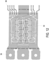
- FIG. 12 schematically shows a power module package employing the conductor proposed in the present disclosure.
- the wire bonds 34 and the lead frame terminals 35 and 36 may adopt the conductor proposed in the present disclosure to damp the high-frequency noise.
- the traces on the substrate and the clops may also adopt the conductor proposed in the present disclosure.
Landscapes
- Engineering & Computer Science (AREA)
- Physics & Mathematics (AREA)
- Electromagnetism (AREA)
- Microelectronics & Electronic Packaging (AREA)
- Power Engineering (AREA)
- Shielding Devices Or Components To Electric Or Magnetic Fields (AREA)
Abstract
A power electronic system with conductor (1a) having damping function is provided. The power electronic system includes power components and a conductor (1a). The conductor (1a) is configured to connect the power components, and includes a damping part (11a) disposed on a surface of the conductor (1a). The damping part (11a) is at least partially formed with a damping material having different resistances at different frequencies, and a relative permeability of the damping material is greater than 1 at a frequency higher than 1MHz. The damping part forms first and second paths for first and second power currents flowing between the power components respectively, the first power current is at a frequency higher than 1MHz, the second power current is at a frequency lower than 1MHz, and a resistance of the first path is higher than a resistance of the second path.
Description
- The present disclosure relates to a power electronic system, and more particularly to a power electronic system with conductors having damping function.
- Power electronic systems with high capacity and power density are increasingly demanded in transportation electrification and smart grid applications. With the recent development of SiC devices, power electronic systems are able to achieve high efficiency and high power density. However, the fast switching speed combined with the parasitic parameters of the package and PCB (printed circuit board) layout inevitably generate high EMI (electromagnetic interference) noises. The high-frequency noises could lead to device and system failure. The EMI noises could also cause the power electronic system to fail EMC (electromagnetic compatibility) regulations.
- The bulky EMI filters are usually used for EMI reduction. Before adding the EMI filters, approaches are needed to reduce or dampen the EMI noise on the board/package level to make sure that the noise would not affect the normal operation of the system.
- Therefore, there is a need of providing a power electronic system with a conductor having damping function in order to overcome the drawbacks of the conventional technologies.
- The present disclosure provides a power electronic system with a conductor having damping function. In the power electronic system of the present disclosure, the high-frequency would flow through a high-resistance path and decrease due to the power loss.
- In accordance with an aspect of the present disclosure, a power electronic system is provided. The power electronic system includes power components and a conductor. The conductor is configured to connect the power components, and includes a damping part disposed on a surface of the conductor. The damping part is at least partially formed with a damping material having different resistances at different frequencies, and a relative permeability of the damping material is greater than 1 at a frequency higher than 1MHz. The damping part forms first and second paths for first and second power currents flowing between the power components respectively, the first power current is at a frequency higher than 1MHz, the second power current is at a frequency lower than 1MHz, and a resistance of the first path is higher than a resistance of the second path.
- In accordance with another aspect of the present disclosure, a power electronic system is provided. The power electronic system includes power components and a conductor. The conductor is configured to connect the power components, and includes a damping part on a surface of the conductor. The damping part has an average roughness greater than 20µm and/or a maximum height roughness greater than 50µm.
- The above contents of the present disclosure will become more readily apparent to those ordinarily skilled in the art after reviewing the following detailed description and accompanying drawings, in which:
-
-
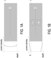
FIG. 1A schematically shows the current distribution in a conductor at low frequencies; -
FIG. 1B schematically shows the current distribution in the conductor at high frequencies; -
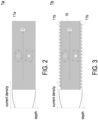
FIG. 2 is a schematic cross-sectional view illustrating a conductor according to a first embodiment of the present disclosure; -
FIG. 3 is a schematic cross-sectional view illustrating a conductor according to a second embodiment of the present disclosure; -
FIG. 4 is a schematic cross-sectional view illustrating a conductor according to a third embodiment of the present disclosure; -
FIG. 5 is a schematic cross-sectional view illustrating a conductor according to a fourth embodiment of the present disclosure; -
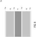
FIG. 6 is a schematic cross-sectional view illustrating a conductor according to a fifth embodiment of the present disclosure; -
FIG. 7A is a schematic cross-sectional view illustrating a conductor according to a sixth embodiment of the present disclosure; -
FIG. 7B schematically shows the current distribution in different portions of the conductor ofFIG. 7A under different frequencies; -
FIG. 8A ,FIG. 8B andFIG. 8C are schematic perspective views illustrating conductors with different appearances on the surface; -
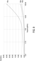
FIG. 9 schematically shows the curves of the resistances of the conductors ofFIGS. 8A ,8B and8C versus the frequency; -
FIG. 10 schematically shows a circuit topology employing the conductor proposed in the present disclosure; -
FIG. 11 schematically shows a device package employing the conductor proposed in the present disclosure; and -
FIG. 12 schematically shows a power module package employing the conductor proposed in the present disclosure. - The present disclosure will now be described more specifically with reference to the following embodiments. It is to be noted that the following descriptions of preferred embodiments of this disclosure are presented herein for purpose of illustration and description only. It is not intended to be exhaustive or to be limited to the precise form disclosed.
- In the present disclosure, a damping technique is proposed to reduce the high-frequency EMI noise in power electronic systems. The damping technique could help reducing the high-frequency EMI noise caused by the power devices during switching, power electronic systems operation, and device paralleling. The proposed damping technique is an easy-to-implement low-cost technique that leverages the natural behavior of conductors to damp the high-frequency noise in power electronic systems. The proposed damping technique and power electronic system could achieve high efficiency, high power density and good reliability.
- Please refer to
FIG. 1A and FIG. 1B. FIG. 1A schematically shows the current distribution in a conductor at low frequencies, andFIG. 1B schematically shows the current distribution in the conductor at high frequencies. InFIG. 1A and FIG. 1B , a current I flows through aconductor 1, and the current distribution is shown by the relations between the current density and the depth in theconductor 1. When the current I is at a low frequency, e.g., lower than 1MHz, as shown inFIG. 1A , the current density in different depths of theconductor 1 are close, namely the current I is evenly distributed in theconductor 1. When the current I is at a high frequency, e.g., higher than 1MHz, as shown inFIG. 1B , the current density at the surface of theconductor 1 is high, while the current density in the middle of theconductor 1 is quite low. In other words, due to the skin and proximity effect, the current I naturally crowds to the skin of theconductor 1. Further, the eddy current generated accordingly is also shown in the figure. - Under high frequencies, the skin depth δ may be obtained according to equation (1).

- In equation (1), ω is the angular frequency, σ is the conductivity, and µ is the permeability. The nature of skin and proximity effect means that the high-frequency current can choose a path different from the low-frequency current to flow.
- Since the current I naturally crowds to the skin of the
conductor 1 under high frequencies, the present disclosure proposes the conductor with damping function at least on the surface of the conductor to increase the high-frequency resistance for damping the high-frequency noise. The proposed conductor is configured to connect the power components of power electronic systems, thereby improving the efficiency, power density and reliability of power electronic systems. For ease of understanding, several implementations of the conductor are exemplified as follows. - Please refer to
FIG. 2. FIG. 2 is a schematic cross-sectional view illustrating a conductor according to a first embodiment of the present disclosure. InFIG. 2 , the current distribution of the current I at a high frequency is also shown. As shown inFIG. 2 , theconductor 1a includes a dampingpart 11a formed with a damping material. The damping material has different resistances at different frequencies, and a relative permeability of the damping material is greater than one at a frequency higher than 1MHz. Due to the characteristics of the damping material, the dampingpart 11a forms first and second paths for first and second power currents flowing between the power components through theconductor 1a respectively. The first power current is at a high frequency (e.g., higher than 1MHz), the second power current is at a low frequency (e.g., lower than 1MHz), and a resistance of the first path is higher than a resistance of the second path. In an embodiment, the damping material has low conductivity and high permeability, such as nickel, iron and aluminum. In an embodiment, the damping material is considered to have permeability higher than copper and conductivity lower than copper. - In addition, the
conductor 1a in this embodiment is entirely formed by the damping material, but the present disclosure is not limited thereto. For instance, in another embodiment, the damping material may form only a section of the conductor. - Please refer to
FIG. 3. FIG. 3 is a schematic cross-sectional view illustrating a conductor according to a second embodiment of the present disclosure. As shown inFIG. 3 , theconductor 1b includes a dampingpart 11b on a surface of theconductor 1b. The dampingpart 11b has an average roughness (Ra) greater than 20µm and/or a maximum height roughness (Rz) greater than 50µm. In one embodiment, the dampingpart 11b has an average roughness (Ra) greater than 20µm. In another embodiment, the dampingpart 11b has a maximum height roughness (Rz) greater than 50µm. In a further embodiment, the dampingpart 11b has an average roughness (Ra) greater than 20µm and a maximum height roughness (Rz) greater than 50µm. Accordingly, the dampingpart 11b forms a rough surface of theconductor 1b, which provide a high resistance. Therefore, when the current I is at a high frequency, the current I naturally crowds to the skin of theconductor 1b and flows through the rough surface with high resistance. Thereby, the high-frequency noise is reduced. - Please refer to
FIG. 4. FIG. 4 is a schematic cross-sectional view illustrating a conductor according to a third embodiment of the present disclosure. As shown inFIG. 4 , theconductor 1c includes a dampingpart 11c disposed on a surface of theconductor 1c and formed with the damping material mentioned above. When the current I is at a high frequency, the current I naturally crowds to the skin of theconductor 1b and flows through the dampingpart 11c with high resistance. Thereby, the high-frequency noise is reduced. - Please refer to
FIG. 5. FIG. 5 is a schematic cross-sectional view illustrating a conductor according to a fourth embodiment of the present disclosure. Theconductor 1d combines the features of theconductors FIG. 5 , theconductor 1d includes a dampingpart 11d, and the dampingpart 11d includes afirst layer 12 and asecond layer 13. Similarly with the dampingpart 11b ofFIG. 3 , thefirst layer 12 has an average roughness greater than 20µm and/or a maximum height roughness greater than 50µm, and provides a high resistance. In one embodiment, thefirst layer 12 has an average roughness greater than 20µm and provides a high resistance. In addition, in another embodiment, thefirst layer 12 has a maximum height roughness greater than 50µm and provides a high resistance. In further another embodiment, thefirst layer 12 has an average roughness greater than 20µm and a maximum height roughness greater than 50µm and provides a high resistance. Thesecond layer 13 is disposed on thefirst layer 12 and is formed with the damping material mentioned above. It is noted that thefirst layer 12 is covered by thesecond layer 13 in this embodiment, while in another embodiment, thesecond layer 13 may be configured to fill in indentations of thefirst layer 12 without completely covering thefirst layer 12. - It is noted that the shape of the conductor is not limited, and the damping part may be disposed on the partial or entire surface of the conductor. For example, the conductor may be cylindrical (e.g., wiring), rectangle or other suitable shape. Moreover, when the conductor has two opposite surfaces, the conductor may include two damping parts on the two opposite surfaces (e.g.,
FIG. 3 ,FIG. 4 and FIG. 5 ), or may include only one damping part on one surface. Furthermore, if the conductor includes two damping parts, each being at least partially formed with the damping material, on the two opposite surfaces, the damping materials forming the two damping parts may be different but both meet the above definition of the damping material. - In addition, in the embodiments shown in
FIG. 3 ,FIG. 4 and FIG. 5 , each of theconductors body part 10, and each of the dampingparts body part 10. Thebody part 10 is for example but not limited to be made of copper, which is widely used in conventional conductors. TakingFIG. 4 as an example, a way of determining the dimensions ofconductor 1c is exemplified as follows. The relations between the dimensions ofconductor 1c and the thickness, conductivity and resistance ofbody part 10 are shown in equation (2).
- In equation (2), tm is the thickness of the
body part 10, l 0 is the specific length of theconductor 1c, σm is the conductivity of thebody part 10, d is the effective width of thebody part 10, and Rm is the resistance of thebody part 10. According to the foregoing descriptions, thebody part 10 forms the main path for transmitting the low-frequency current. Therefore, given a desired resistance at low frequency, the thickness tm of thebody part 10 can be calculated through equation (2). - Further, an equation associated with the resistance of the layer formed with the damping material, i.e., the damping
part 11c, is shown as:
- In equation (3), Rs is the resistance of the damping
part 11c, τr is the surface roughness coefficient, ω is the angular frequency, µr is the relative permeability of the damping material, µi is the initial permeability, and σs is the conductivity of the damping material. As the angular frequency ω and the resistance Rs are defined to damp the high-frequency noise, the specific length l 0 and effective width d (i.e., the dimensions) of theconductor 1c can be calculated through equation (3). Additionally, based on equation (3), increasing the surface roughness would increase the surface roughness coefficient τr , resulting in higher resistance Rs. Namely, in theconductor 1d ofFIG. 5 , thefirst layer 12 of dampingpart 11d which forms a rough surface would further increase the resistance of dampingpart 11d. - Additionally, in the present disclosure, the conductor may be a multi-layer structure. Please refer to
FIG. 6. FIG. 6 is a schematic cross-sectional view illustrating a conductor according to a fifth embodiment of the present disclosure. As shown inFIG. 6 , theconductor 1c includes a plurality ofbody part 10 and a plurality of dampingparts 11e, and each dampingpart 11e is formed with the damping material defined above. Two opposite surfaces of eachbody part 10 are covered by two dampingparts 11e respectively. Further, in theconductor 1c, any twobody parts 10 neighboring to each other are insulated by aninsulation layer 14 formed with insulation material. It is noted that the specific materials that form the plurality of dampingparts 11e respectively may be identical or different, but all meet the definition of the damping material of the present disclosure. - Please refer to
FIG. 7A andFIG. 7B .FIG. 7A is a schematic cross-sectional view illustrating a conductor according to a sixth embodiment of the present disclosure. As shown inFIG. 7A , theconductor 1f includes twobody parts insulation layer 14 and a dampingpart 11f. Theinsulation layer 14 is between thebody parts body parts part 11f is disposed on thebody part 10a. InFIG. 7A , a current direction D1 and an observation line D2 are shown. Along the observation line D2, A1, A2, A3 and A4 represent the regions of thebody part 10b, theinsulation layer 14, thebody part 10a and the dampingpart 11f respectively.FIG. 7B schematically shows the current distribution in different portions of the conductor ofFIG. 7A under different frequencies. InFIG. 7B , the current distribution under the frequencies of 100kHz, 100MHz and 1GHz are depicted by solid line, dashed line and dot chain line, respectively. As shown inFIG. 7A andFIG. 7B , under 100kHz, the current mainly flows through thebody part 10a; under 100MHz, the current mainly flows through the dampingpart 11f; and under 1GHz, the current mainly flows through the dampingpart 11f and thebody part 10b. -
FIG. 8A ,FIG. 8B andFIG. 8C are schematic perspective views illustrating conductors with different appearances on the surface. InFIG. 8A , theconductor 2a includes abody part 20 with a smooth surface. InFIG. 8B , theconductor 2b includes abody part 20 and a rough layer 21 (thread). Therough layer 21 is disposed on thebody part 20 and has an average roughness greater than 20µm and/or a maximum height roughness greater than 50µm. In one embodiment, therough layer 21 is disposed on thebody part 20 and has an average roughness greater than 20µm. In another embodiment, therough layer 21 is disposed on thebody part 20 and has a maximum height roughness greater than 50µm. In further another embodiment, therough layer 21 is disposed on thebody part 20 and has an average roughness greater than 20µm and a maximum height roughness greater than 50µm. InFIG. 8C , the conductor 2c includes abody part 20, arough layer 21 and a dampingmaterial 22. Therough layer 21 is similar with that shown inFIG. 8B . The dampingmaterial 22 meets the definition of the above-mentioned damping material and is filled in indentations of therough layer 21. -
FIG. 9 schematically shows the curves of the resistances of the conductors ofFIGS. 8A ,8B and8C versus the frequency. InFIG. 9 , R2a, R2b and R2c represents the resistances of theconductors FIGS. 8A ,8B and8C respectively. As shown inFIG. 9 , when the frequency is lower than 1MHz, the resistances R2a and R2b are nearly the same, and the resistance R2c is greater than the resistances R2a and R2b. When the frequency is higher than 1MHz, the resistance R2b gradually increases to be larger than the resistance R2a. When the frequency is 100MHz, the resistance R2c is much greater than the resistances R2a and R2b. It can be seen that the damping material can greatly increase the resistance under high frequency, and thus the high-frequency noise can be effectively reduced. - In the present disclose, the proposed conductor is configured to connect the power components of the power electronic system. It is noted that the specific implementations of the power electronic system and the power components thereof are not limited. In other words, the conductor may be used in various kinds of power electronic system for damping the high-frequency noise. For instance, the proposed conductor may be configured as a trace of a printed circuit board, a terminal pin of a device package, or a trace, a clip or a lead frame terminal of a power module package, but not exclusively. Some examples are exemplified as follows.
-
FIG. 10 schematically shows a circuit topology employing the conductor proposed in the present disclosure. As shown inFIG. 10 , theswitch components 31 are connected through theconductors 32, and theconductors 32 may be implemented by the conductor proposed in the present disclosure to damp the high-frequency noise. For instance, theswitch components 31 may be the power components on a printed circuit board, and theconductors 32 may be the traces of the printed circuit board. -
FIG. 11 schematically shows a device package employing the conductor proposed in the present disclosure. As shown inFIG. 11 , thepins 33 of the device package may adopt the conductor proposed in the present disclosure the damp the high-frequency noise. -
FIG. 12 schematically shows a power module package employing the conductor proposed in the present disclosure. As shown inFIG. 12 , thewire bonds 34 and thelead frame terminals FIG. 12 , the traces on the substrate and the clops may also adopt the conductor proposed in the present disclosure.
Claims (13)
- A power electronic system, characterized by comprising:power components; anda conductor (1), configured to connect the power components, and comprising a damping part (11a) disposed on a surface of the conductor (1), wherein the damping part (11a) is at least partially formed with a damping material having different resistances at different frequencies, and a relative permeability of the damping material is greater than 1 at a frequency higher than 1MHz,wherein the damping part (11a) forms first and second paths for first and second power currents flowing between the power components respectively, the first power current is at a frequency higher than 1MHz, the second power current is at a frequency lower than 1MHz, and a resistance of the first path is higher than a resistance of the second path.
- The power electronic system according to claim 1, wherein the damping part (11d) comprises a first layer (12) and a second layer (13), the first layer (12) has an average roughness greater than 20µm and/or a maximum height roughness greater than 50µm, and the second layer (13) is disposed on the first layer (12) and is formed by the damping material.
- The power electronic system according to claim 2, wherein the first layer (12) is covered by the second layer (13).
- The power electronic system according to claim 2, wherein the second layer (22) is configured to fill in indentations of the first layer (21).
- The power electronic system according to claim 2, wherein the conductor (1d) comprises two said damping parts (11d) on two opposite surfaces of the conductor (1d).
- The power electronic system according to claim 5, wherein two second layers (13) of the two damping parts (11d) are formed by a first material and a second material, which are different and are both comprised by the damping material, respectively.
- The power electronic system according to claim 1, wherein the conductor (1c) comprises two said damping parts (11c) on two opposite surfaces of the conductor (1c).
- The power electronic system according to claim 7, wherein the two damping parts (11c) are formed by a first material and a second material, which are different and are both comprised by the damping material, respectively.
- The power electronic system according to claim 1, wherein the conductor (1e) comprises a plurality of body parts (10), two opposite surfaces of each of the plurality of body parts (10) are covered by two said damping parts (11e) respectively, and any two of the plurality of body parts (10) neighboring to each other are insulated by an insulation layer (14).
- The power electronic system according to claim 1, wherein the damping material comprises nickel, iron and aluminum.
- The power electronic system according to claim 1, wherein the conductor (1a) is configured as a trace of a printed circuit board, a terminal pin (33) of a device package, or a trace, a clip or a lead frame terminal (35, 36) of a power module package.
- A power electronic system, characterized by comprising:power components; anda conductor (1b), configured to connect the power components, and comprising a damping part (11b) on a surface of the conductor (1b), wherein the damping part (11b) has an average roughness greater than 20µm and/or a maximum height roughness greater than 50µm.
- The power electronic system according to claim 12, wherein the conductor (1b) comprises two said damping parts (11b) on two opposite surfaces of the conductor (1b).
Applications Claiming Priority (1)
| Application Number | Priority Date | Filing Date | Title |
|---|---|---|---|
| US202363611814P | 2023-12-19 | 2023-12-19 |
Publications (1)
| Publication Number | Publication Date |
|---|---|
| EP4576970A1 true EP4576970A1 (en) | 2025-06-25 |
Family
ID=93925925
Family Applications (1)
| Application Number | Title | Priority Date | Filing Date |
|---|---|---|---|
| EP24221114.2A Pending EP4576970A1 (en) | 2023-12-19 | 2024-12-18 | Power electronic system with conductor having damping function |
Country Status (3)
| Country | Link |
|---|---|
| US (1) | US20250239378A1 (en) |
| EP (1) | EP4576970A1 (en) |
| CN (1) | CN120185374A (en) |
Citations (2)
| Publication number | Priority date | Publication date | Assignee | Title |
|---|---|---|---|---|
| US20120032330A1 (en) * | 2008-10-21 | 2012-02-09 | International Business Machines Corporation | Mitigation of plating stub resonance by controlling surface roughness |
| US20190393161A1 (en) * | 2018-06-26 | 2019-12-26 | Abb Schweiz Ag | Multi-layer conductors for noise reduction in power electronics |
-
2024
- 2024-12-18 US US18/985,924 patent/US20250239378A1/en active Pending
- 2024-12-18 CN CN202411871523.3A patent/CN120185374A/en active Pending
- 2024-12-18 EP EP24221114.2A patent/EP4576970A1/en active Pending
Patent Citations (2)
| Publication number | Priority date | Publication date | Assignee | Title |
|---|---|---|---|---|
| US20120032330A1 (en) * | 2008-10-21 | 2012-02-09 | International Business Machines Corporation | Mitigation of plating stub resonance by controlling surface roughness |
| US20190393161A1 (en) * | 2018-06-26 | 2019-12-26 | Abb Schweiz Ag | Multi-layer conductors for noise reduction in power electronics |
Non-Patent Citations (2)
| Title |
|---|
| TIMSIT R S: "High Speed Electronic Connector Design: A Review of Electrical and Electromagnetic Properties of Passive Contact Elements - Part 1", IEICE TRANSACTIONS ON ELECTRONICS, INSTITUTE OF ELECTRONICS, TOKYO, JP, vol. E91C, no. 8, 1 August 2008 (2008-08-01), pages 1178 - 1191, XP001515942, ISSN: 0916-8524, DOI: 10.1093/IETELE/E91-C.8.1178 * |
| TIMSIT R S: "HIGH SPEED LELECTRONIC CONNECTORS: A REVIEW OF ELECTRICAL CONTACT PROPERTIES", IEICE TRANSACTIONS ON ELECTRONICS, INSTITUTE OF ELECTRONICS, TOKYO, JP, vol. E88-C, no. 8, 1 August 2005 (2005-08-01), pages 1532 - 1545, XP001232830, ISSN: 0916-8524, DOI: 10.1093/IETELE/E88-C.8.1532 * |
Also Published As
| Publication number | Publication date |
|---|---|
| CN120185374A (en) | 2025-06-20 |
| US20250239378A1 (en) | 2025-07-24 |
Similar Documents
| Publication | Publication Date | Title |
|---|---|---|
| EP1232679B1 (en) | Printed circuit board employing lossy power distribution network to reduce power plane resonances | |
| US6621012B2 (en) | Insertion of electrical component within a via of a printed circuit board | |
| US7047628B2 (en) | Impedance matching of differential pair signal traces on printed wiring boards | |
| US6798666B1 (en) | Introducing loss in a power bus to reduce EMI and electrical noise | |
| US9214713B2 (en) | Method of fabricating a microstrip line dielectric overlay | |
| US8344821B2 (en) | Differential transmission line printed circuit board layout based on eye diagram parameters | |
| CN203040005U (en) | Printed circuit board | |
| US8227709B2 (en) | Printed wiring board, and design method for printed wiring board | |
| JP2002111324A (en) | Circuit board for signal transmission, method of manufacturing the same, and electronic equipment using the same | |
| JP2013187249A (en) | Transmission line structure, multilayer wiring board, semiconductor device, and semiconductor system | |
| JP2008527724A (en) | Printed circuit boards with improved signal integrity for differential signal pairs, etc. | |
| US8040201B2 (en) | Substrate having a structure for suppressing noise generated in a power plane and/or a ground plane, and an electronic system including the same | |
| US20050083147A1 (en) | Circuit board and method in which the impedance of a transmission-path is selected by varying at least one opening in a proximate conductive plane | |
| US6999330B2 (en) | Power converter and system using the same | |
| JP4933318B2 (en) | Printed circuit board assembly and inverter using the printed circuit board assembly | |
| US8324508B2 (en) | Composite circuit board | |
| US20250239378A1 (en) | Power electronic system with conductor having damping function | |
| US6181571B1 (en) | Printed-wiring board and electronic device having the same wiring board | |
| US7196906B1 (en) | Circuit board having segments with different signal speed characteristics | |
| CN219919248U (en) | Printed circuit board structure | |
| US11452202B2 (en) | Radio frequency filtering of printed wiring board direct current distribution layer | |
| CN219536387U (en) | Printed circuit board structure | |
| KR100594298B1 (en) | Multipath Printed Circuit Board with Dissimilar Metal Layers and Power Supply System | |
| CN219577353U (en) | Printed circuit board structure | |
| JP2007189042A (en) | Semiconductor device |
Legal Events
| Date | Code | Title | Description |
|---|---|---|---|
| PUAI | Public reference made under article 153(3) epc to a published international application that has entered the european phase |
Free format text: ORIGINAL CODE: 0009012 |
|
| STAA | Information on the status of an ep patent application or granted ep patent |
Free format text: STATUS: THE APPLICATION HAS BEEN PUBLISHED |
|
| AK | Designated contracting states |
Kind code of ref document: A1 Designated state(s): AL AT BE BG CH CY CZ DE DK EE ES FI FR GB GR HR HU IE IS IT LI LT LU LV MC ME MK MT NL NO PL PT RO RS SE SI SK SM TR |
|
| STAA | Information on the status of an ep patent application or granted ep patent |
Free format text: STATUS: REQUEST FOR EXAMINATION WAS MADE |
|
| 17P | Request for examination filed |
Effective date: 20251219 |