EP4576568A1 - System and method for increasing transconductance of a cmos inverter - Google Patents
System and method for increasing transconductance of a cmos inverter Download PDFInfo
- Publication number
- EP4576568A1 EP4576568A1 EP23219084.3A EP23219084A EP4576568A1 EP 4576568 A1 EP4576568 A1 EP 4576568A1 EP 23219084 A EP23219084 A EP 23219084A EP 4576568 A1 EP4576568 A1 EP 4576568A1
- Authority
- EP
- European Patent Office
- Prior art keywords
- supply voltage
- cmos inverter
- inverter
- transconductance
- biasing circuit
- Prior art date
- Legal status (The legal status is an assumption and is not a legal conclusion. Google has not performed a legal analysis and makes no representation as to the accuracy of the status listed.)
- Pending
Links
Images


Classifications
-
- H—ELECTRICITY
- H03—ELECTRONIC CIRCUITRY
- H03F—AMPLIFIERS
- H03F1/00—Details of amplifiers with only discharge tubes, only semiconductor devices or only unspecified devices as amplifying elements
- H03F1/02—Modifications of amplifiers to raise the efficiency, e.g. gliding Class A stages, use of an auxiliary oscillation
- H03F1/0205—Modifications of amplifiers to raise the efficiency, e.g. gliding Class A stages, use of an auxiliary oscillation in transistor amplifiers
- H03F1/0211—Modifications of amplifiers to raise the efficiency, e.g. gliding Class A stages, use of an auxiliary oscillation in transistor amplifiers with control of the supply voltage or current
-
- H—ELECTRICITY
- H03—ELECTRONIC CIRCUITRY
- H03K—PULSE TECHNIQUE
- H03K19/00—Logic circuits, i.e. having at least two inputs acting on one output; Inverting circuits
- H03K19/02—Logic circuits, i.e. having at least two inputs acting on one output; Inverting circuits using specified components
- H03K19/08—Logic circuits, i.e. having at least two inputs acting on one output; Inverting circuits using specified components using semiconductor devices
- H03K19/094—Logic circuits, i.e. having at least two inputs acting on one output; Inverting circuits using specified components using semiconductor devices using field-effect transistors
- H03K19/0944—Logic circuits, i.e. having at least two inputs acting on one output; Inverting circuits using specified components using semiconductor devices using field-effect transistors using MOSFET or insulated gate field-effect transistors, i.e. IGFET
- H03K19/0948—Logic circuits, i.e. having at least two inputs acting on one output; Inverting circuits using specified components using semiconductor devices using field-effect transistors using MOSFET or insulated gate field-effect transistors, i.e. IGFET using CMOS or complementary insulated gate field-effect transistors
-
- G—PHYSICS
- G05—CONTROLLING; REGULATING
- G05F—SYSTEMS FOR REGULATING ELECTRIC OR MAGNETIC VARIABLES
- G05F3/00—Non-retroactive systems for regulating electric variables by using an uncontrolled element, or an uncontrolled combination of elements, such element or such combination having self-regulating properties
- G05F3/02—Regulating voltage or current
- G05F3/08—Regulating voltage or current wherein the variable is DC
- G05F3/10—Regulating voltage or current wherein the variable is DC using uncontrolled devices with non-linear characteristics
- G05F3/16—Regulating voltage or current wherein the variable is DC using uncontrolled devices with non-linear characteristics being semiconductor devices
- G05F3/20—Regulating voltage or current wherein the variable is DC using uncontrolled devices with non-linear characteristics being semiconductor devices using diode- transistor combinations
- G05F3/205—Substrate bias-voltage generators
-
- H—ELECTRICITY
- H03—ELECTRONIC CIRCUITRY
- H03F—AMPLIFIERS
- H03F1/00—Details of amplifiers with only discharge tubes, only semiconductor devices or only unspecified devices as amplifying elements
- H03F1/02—Modifications of amplifiers to raise the efficiency, e.g. gliding Class A stages, use of an auxiliary oscillation
- H03F1/0205—Modifications of amplifiers to raise the efficiency, e.g. gliding Class A stages, use of an auxiliary oscillation in transistor amplifiers
- H03F1/0261—Modifications of amplifiers to raise the efficiency, e.g. gliding Class A stages, use of an auxiliary oscillation in transistor amplifiers with control of the polarisation voltage or current, e.g. gliding Class A
-
- H—ELECTRICITY
- H03—ELECTRONIC CIRCUITRY
- H03F—AMPLIFIERS
- H03F1/00—Details of amplifiers with only discharge tubes, only semiconductor devices or only unspecified devices as amplifying elements
- H03F1/30—Modifications of amplifiers to reduce influence of variations of temperature or supply voltage or other physical parameters
- H03F1/301—Modifications of amplifiers to reduce influence of variations of temperature or supply voltage or other physical parameters in MOSFET amplifiers
-
- H—ELECTRICITY
- H03—ELECTRONIC CIRCUITRY
- H03F—AMPLIFIERS
- H03F1/00—Details of amplifiers with only discharge tubes, only semiconductor devices or only unspecified devices as amplifying elements
- H03F1/30—Modifications of amplifiers to reduce influence of variations of temperature or supply voltage or other physical parameters
- H03F1/307—Modifications of amplifiers to reduce influence of variations of temperature or supply voltage or other physical parameters in push-pull amplifiers
-
- H—ELECTRICITY
- H03—ELECTRONIC CIRCUITRY
- H03F—AMPLIFIERS
- H03F1/00—Details of amplifiers with only discharge tubes, only semiconductor devices or only unspecified devices as amplifying elements
- H03F1/32—Modifications of amplifiers to reduce non-linear distortion
- H03F1/3205—Modifications of amplifiers to reduce non-linear distortion in field-effect transistor amplifiers
-
- H—ELECTRICITY
- H03—ELECTRONIC CIRCUITRY
- H03F—AMPLIFIERS
- H03F3/00—Amplifiers with only discharge tubes or only semiconductor devices as amplifying elements
- H03F3/30—Single-ended push-pull [SEPP] amplifiers; Phase-splitters therefor
- H03F3/3001—Single-ended push-pull [SEPP] amplifiers; Phase-splitters therefor with field-effect transistors
- H03F3/3022—CMOS common source output SEPP amplifiers
-
- H—ELECTRICITY
- H03—ELECTRONIC CIRCUITRY
- H03K—PULSE TECHNIQUE
- H03K19/00—Logic circuits, i.e. having at least two inputs acting on one output; Inverting circuits
- H03K19/003—Modifications for increasing the reliability for protection
- H03K19/00369—Modifications for compensating variations of temperature, supply voltage or other physical parameters
- H03K19/00384—Modifications for compensating variations of temperature, supply voltage or other physical parameters in field effect transistor circuits
-
- H—ELECTRICITY
- H03—ELECTRONIC CIRCUITRY
- H03F—AMPLIFIERS
- H03F2200/00—Indexing scheme relating to amplifiers
- H03F2200/453—Controlling being realised by adding a replica circuit or by using one among multiple identical circuits as a replica circuit
Definitions
- the invention relates to the enhancement of the performance of inverter-based circuits, especially to the enhancement of the transconductance range of the Complementary Metal-Oxide Semiconductor (CMOS) inverter of the inverter-based circuits.
- CMOS Complementary Metal-Oxide Semiconductor
- Radio frequency (RF) receivers may include many inverter-based circuits, such as Low-Noise Transconductance Amplifiers (LNTAs), Transimpedance Amplifiers (TIAs), LowPass Filters (LPFs), to reduce the overall power and to increase the linearity.
- LNTAs Low-Noise Transconductance Amplifiers
- TIAs Transimpedance Amplifiers
- LPFs LowPass Filters
- the transconductance of the inverters of the inverter-based circuits may be controlled across the temperature and supply voltage variations in order to achieve an optimal performance.
- an object of the invention is to provide a system and a method for increasing the transconductance range of a CMOS inverter, especially beyond the typical supply voltage of the CMOS inverter.
- the transconductance range of the CMOS inverter can be extended beyond the range provided by the supply voltage by the application of the bias voltage at the interconnected back gates of the respective transistors.
- the control circuit may facilitate an automatic control of the transconductance of the CMOS inverter over the extended transconductance range of the CMOS inverter.
- the transistor arrangement is configured to control the transconductance of the CMOS inverter by means of the replicated CMOS inverter and the resistor.
- the transconductance of the CMOS inverter can be effectively controlled via a resistor value, especially via the tunable resistor, across voltage and temperature in order to compensate for the voltage and temperature variations.
- the resistor value may be a known resistor value, which may facilitate an effective tuning of the resistor.
- the transistor arrangement of the biasing circuit is configured to control the transconductance of the CMOS inverter for the supply voltage ranging from the predefined minimum value to the threshold value.
- the transconductance is inversely proportional to the resistor of the transistor arrangement.
- a maximum possible linearity of the transconductance of the CMOS inverter over the transconductance range can be achieved.
- the method comprises the step of providing, by a control circuit, a bias voltage to the interconnected back gates when the supply voltage reaches to a threshold value. Moreover, the method comprises the step of controlling, together by the biasing circuit and the control circuit, the transconductance of the CMOS inverter.
- the inverter 101 may correspond to any inverter-based blocks, especially to any inverter-based blocks, such as LNTA, TIAs, LPF, of an RF receiver.
- the inverter 101 may comprise one or more FDSOI transistors, especially one FDSOI PMOS transistor and one FDSOI NMOS transistor arranged in a complementary manner.
- the system 100 may comprise a control circuit 103 connected to the supply line 104 and further to the bias line 105.
- the control circuit 103 may continuously sense or monitor the supply voltage Vd at the supply line, and may compare the supply voltage Vd with a threshold voltage Vt.
- control circuit 103 may provide the bias voltage Vbg to the interconnected back gates, e.g., via the bias line 105, when the supply voltage Vd becomes equal to the threshold voltage Vt. However, if the supply voltage Vd is less than the threshold voltage Vt, the control circuit 103 may maintain the supply voltage Vd and may set the bias voltage Vbg to zero.
- the bias circuit 102 and the control circuit 103 may collectively control the Gm range of the inverter 101, especially to increase the Gm range beyond the range limited by the supply voltage Vd, by means of the additional bias voltage Vbg at the interconnected back gates of the respective FDSOI transistors.
- control circuit 103 may provide an automatic control of the Gm of the inverter 101 over the extended Gm range of the inverter 101.
- FIG. 2 an exemplary algorithm 200 of the system 100 is illustrated via a process flow diagram. It is to be noted that, for simplicity, the implementation regarding the bias voltage Vbg is illustrated for the NMOS transistor of the CMOS inverter 101.
- the biasing circuit 102 may supply the supply voltage Vd to the inverter 101 and further to the inverter arrangement of the biasing circuit 102, especially to ensure the proper operation of the inverter 101.
- the control circuit 103 may be connected to the supply line 104 and further to the bias line 105 that may interconnect the back gates of the respective transistors of the biasing circuit 102 and the inverter 101.
- control circuit 103 may sense whether the supply voltage Vd is less than the threshold voltage Vt or is equal to the threshold voltage Vt.
- control circuit 103 may only maintain the supply voltage Vd by setting the bias voltage Vbg to zero, thereby resulting a phase 204 of the process flow.
- the control circuit may maintain the supply voltage Vd and may additionally supply the bias voltage Vbg to the interconnected back gates of the respective transistors, thereby resulting an alternative phase 205 of the process flow.
- the process flow diagram may result in the following use case scenario in order to maintain a constant transconductance over temperature and supply voltage variations:
- process flow from 203 to 205 may be used for a further scenario that may require an inverter with a Gm, which is higher than the Gm range solely provided by the supply voltage Vd of the inverter.
- Fig. 3A an exemplary relationship between the Gm and the supply of CMOS inverters is illustrated, where the Gm is especially controlled by a conventional complementary constant-Gm biasing circuit.
- the complementary constant-Gm biasing circuit may control the inverter supply voltage such that the Gm of the inverter is inversely proportional to a control resistor of the complementary constant-Gm biasing circuit. Since the resistor value is well known across supply voltage and temperature, the Gm of the inverter can be controlled over the GM range and further maintained constant at a desired GM value by adjusting the resistance value of the control resistor which in turns adjusts the inverter supply accordingly.
- the Gm of the inverter can be expressed as the ratio of the output current to the input voltage of the inverter. In order to achieve a reliable performance, the Gm should be regulated over supply voltage and temperature variation.
- the control resistor of the complementary constant-Gm biasing circuit may vary the inverter supply in order to determine the Gm of the inverter, where the input and output nodes of the inverter may be unaffected in order not to disturb the signal flow.
- control resistor may control the supply voltage of the inverter in order to control the Gm of the inverter, where the Gm may be limited by the inverter supply voltage as well.
- the horizontal axis denotes the inverter supply voltage and the vertical axis denotes the Gm.
- the lower side of the Gm i.e., the Gmmin
- the minimum inverter supply Vdmin in order to satisfy the minimum linearity criteria of for the inverter
- the upper side of the Gm i.e., the Gmmax
- the complementary constant-Gm biasing circuit stops being operational after reaching Vdmax.
- Fig. 3B an exemplary relationship between the Gm and the supply of the inverter 101 is illustrated according to the first aspect of the invention.
- the back gates of the respective transistors of the biasing circuit 102 and the inverter 101 may be interconnected and may be fed with the bias voltage Vbg by the control circuit 103, thereby extending the inverter supply voltage range.
- the horizontal axis denotes the inverter supply voltage Vd and the bias voltage Vbg.
- the vertical axis denotes the Gm of the inverter 101. It can be seen that, similar to Fig. 3A , the lower side of the Gm, i.e., the Gmmin, is limited is limited by the minimum inverter supply Vdmin in order to satisfy the minimum linearity criteria of for the inverter 101, however, the upper side of the Gm in relation to Fig. 3A , i.e., the Gmmax, is now extended further to Gmgreat, especially due to the application of the bias voltage Vbg to the interconnected back gates while maintaining the supply voltage Vd.
- the biasing circuit 102 may provide the supply voltage Vd to the inverter 101 and the control circuit 103 may continuously sense the supply voltage Vd with respect to the threshold voltage Vt, which is shown here as the maximum inverter supply Vdmax.
- control circuit 103 may exclusively maintain the supply voltage Vd to the inverter 101 over the range Vdmin to Vdmax, especially by setting the bias voltage Vbg at the interconnected back gates to zero.
- the control circuit 103 may apply the bias voltage Vbg to the interconnected back gates while maintaining the supply voltage Vd at its maximum limit Vdmax.
- the Gm of the inverter 101 can be effectively increased from the maximum limit Gmmax of Fig. 3A to a greater limit Gmgreat while simultaneously extending the inverter supply from the maximum limit Vdmax of Fig. 3A to a greater limit Vdmax, which may correspond to the supply voltage of the biasing circuit 102.
- the increase in the bias voltage Vbg is illustrated for the NMOS transistor of the CMOS inverter 101. It is further to be noted that the linear relationship between the Gm and inverter supply, as shown in Fig. 3A and Fig 3B , are shown only for illustration purpose, and the relationship, e.g., the curve, may be of higher order polynomial.
- a second exemplary embodiment of the system 400 according to the first aspect of the invention is illustrated.
- the system 400 exemplarily shows the internal circuital arrangement of the system 100.
- the inverter 101 may comprise the complementary FDSOI NMOS M1 and PMOS M2, where Vi may denote the input voltage and iout may denote the output voltage of the inverter 101.
- the Gm can be expressed as a function of the inverter supply voltage Vd.
- the biasing circuit 102 may correspond to a conventional complementary constant-Gm biasing circuit, where the back gates of the respective transistors of the biasing circuit 102 and the inverter 101 are additionally interconnected.
- the biasing circuit 102 may regulate the inverter supply voltage Vd such that the Gm of the inverter 101 can be maintained constant.
- the biasing circuit 102 may comprise a start-up segment, a current mirror segment, and a control segment.
- the start-up segment of the biasing circuit 102 may comprise a PMOS M12, which may act as the start-up or regulator for the biasing circuit 102 in order to avoid the lower values of the supply vdd of the biasing circuit 102, especially to avoid feeding the lower values of supply voltage Vd to the inverter 101.
- the PMOS M12 may enter in triode region for the upper values of the supply voltage Vd to the inverter 101, thereby limiting the inverter supply voltage Vd to Vd,max.
- the current mirror segment may comprise any CMOS current mirror arrangement known in the art.
- the current mirror branches of the biasing circuit 102 may comprise complementary pairs of PMOS M8 and NMOS M11, and PMOS M10 and NMOS M13 in order to replicate the current from one branch to the other branch.
- control segment of the biasing circuit 102 may comprise a first CMOS block comprising PMOS M4, NMOS M3, and NMOS M7, where the CMOS M3 and M4 pair may be a scaled version of the CMOS M1 and M2 pair of the inverter 101.
- control segment of the biasing circuit 102 may comprise a second CMOS block comprising PMOS M6, NMOS M5, and NMOS M9, where the CMOS M5 and M6 pair may be a scaled version of the CMOS M1 and M2 pair of the inverter 101.
- first CMOS block and the second CMOS block may be connected to the respective current mirror branches of the biasing circuit 102.
- the respective back gates of the transistors of the first CMOS block, the second CMOS block, and the inverter 101 may be interconnected.
- the back gates of the PMOS M4, the PMOS M6, and the PMOS M2 may be interconnected.
- the back gates of the NMOS M3, the NMOS M5, the NMOS M7, the NMOS M9, and the NMOS M1 may be interconnected.
- control circuit 103 may comprise or be an OPAMP 401.
- the non-inverting terminal of the OPAMP 401 may be connected to the inverter supply Vd and the inverting terminal of the OPAMP 401 may be supplied with a reference voltage, namely the threshold voltage Vd,max, such that the OPAMP 401 may compare the supply voltage Vd with the threshold voltage Vd,max.
- the inverting output of the OPAMP 401 may be connected to the interconnected back gates of the PMOS transistors, namely the back gates of the PMOS M2, the PMOS M4, and the PMOS M6.
- the non-inverting output of the OPAMP 401 may be connected to the interconnected back gates of the NMOS transistors, namely the back gates of the NMOS M1, the NMOS M3, the NMOS M5, the NMOS M7, and the NMOS M9.
- the Gm of the CMOS M3/M4 can be expressed as: G m , 34 ⁇ R
- the Gm of the CMOS M1/M2 can be expressed as: G m , 12 ⁇ R
- the resistor R can be varied in order to regulate or to control the G m, 12 , and the resistor R is constant across temperature and supply voltage variations.
- the OPAMP 401 may set the bias voltage V BP to vdd for the interconnected back gates of the PMOS transistors, namely the back gates of the PMOS M2, the PMOS M4, and the PMOS M6, and may set the bias voltage V BN to zero for the interconnected back gates of the NMOS transistors, namely the back gates of the NMOS M1, the NMOS M3, the NMOS M5, the NMOS M7, and the NMOS M9.
- both the control circuit 103 and biasing circuit 102 may together increase the tuning range of the G m, 12 of the inverter 101, whereby simultaneously providing the automatic tuning of the G m ,12 of the inverter 101.
- the Gm,max of the inverter 101 is about 10mS.
- the maximum possible supply voltage range of the inverter is extended to vdd, i.e., the supply of the biasing circuit, and the Gm range of the inverter 101 is extended to about 35mS.
- the vbg,max is the vdd and the Gm,great is about 35mS.
- the transition for the back gate bias voltage V BN from vdd to 0 at the interconnected NMOS transistors is shown in the plot 502.
- the transition for the back gate bias voltage V Bp from 0 to vdd at the interconnected PMOS transistors is shown in the plot 503.
- a supply voltage is provided to a CMOS inverter by a biasing circuit, where at least one transistor arrangement of the biasing circuit and the CMOS inverter are interconnected via back gates of respective transistors.
- a bias voltage is provided to the interconnected back gates by a control circuit when the supply voltage reaches to a threshold value.
- the transconductance of the CMOS inverter is controlled together by the biasing circuit and the control circuit.
Landscapes
- Engineering & Computer Science (AREA)
- Power Engineering (AREA)
- Physics & Mathematics (AREA)
- Mathematical Physics (AREA)
- Computing Systems (AREA)
- General Engineering & Computer Science (AREA)
- Computer Hardware Design (AREA)
- Nonlinear Science (AREA)
- Microelectronics & Electronic Packaging (AREA)
- Electromagnetism (AREA)
- General Physics & Mathematics (AREA)
- Radar, Positioning & Navigation (AREA)
- Automation & Control Theory (AREA)
- Amplifiers (AREA)
Abstract
A system (100) is provided for increasing the transconductance of a CMOS inverter (101). The system comprises a biasing circuit (102) configured to provide a supply voltage (Vd) to the CMOS inverter (101), wherein the biasing circuit (102) comprises at least one transistor arrangement, wherein the transistor arrangement and the CMOS inverter (101) are interconnected via back gates of respective transistors. The system further comprises a control circuit (103) configured to provide a bias voltage (Vbg) to the interconnected back gates when the supply voltage (Vd) reaches to a threshold value (Vt), whereby both the biasing circuit (102) and the control circuit (103) together control the transconductance of the CMOS inverter (101) .
Description
- The invention relates to the enhancement of the performance of inverter-based circuits, especially to the enhancement of the transconductance range of the Complementary Metal-Oxide Semiconductor (CMOS) inverter of the inverter-based circuits.
- Radio frequency (RF) receivers may include many inverter-based circuits, such as Low-Noise Transconductance Amplifiers (LNTAs), Transimpedance Amplifiers (TIAs), LowPass Filters (LPFs), to reduce the overall power and to increase the linearity. For instance, the transconductance of the inverters of the inverter-based circuits may be controlled across the temperature and supply voltage variations in order to achieve an optimal performance.
- For example, the document Jansen et al., Complementary constant-gm biasing of Nauta-transconductors in low-power Gm-C filters to +/-2% accuracy over temperature, Pages 466-469, 2012 Proceedings of the ESSCIRC, 2013, doi: 10.1109/JSSC.2013.2253233 discloses a static complementary constant-transconductance biasing circuit for CMOS inverter-based filters. However, the transconductance range of the CMOS inverter is limited by the supply voltage of the CMOS inverter.
- Accordingly, an object of the invention is to provide a system and a method for increasing the transconductance range of a CMOS inverter, especially beyond the typical supply voltage of the CMOS inverter.
- The object is solved by the features of the first independent claim for the system and by the features of the second independent claim for the method. The dependent claims contain further developments.
- According to a first aspect of the invention, a system is provided for increasing the transconductance of a CMOS inverter. The system comprises a biasing circuit configured to provide a supply voltage to the CMOS inverter, wherein the biasing circuit comprises at least one transistor arrangement, wherein the transistor arrangement and the CMOS inverter are interconnected via back gates of respective transistors.
- In addition, the system comprises a control circuit configured to provide a bias voltage to the interconnected back gates when the supply voltage reaches to a threshold value, whereby both the biasing circuit and the control circuit together control the transconductance of the CMOS inverter.
- Advantageously, the transconductance range of the CMOS inverter can be extended beyond the range provided by the supply voltage by the application of the bias voltage at the interconnected back gates of the respective transistors. Furthermore, the control circuit may facilitate an automatic control of the transconductance of the CMOS inverter over the extended transconductance range of the CMOS inverter.
- Preferably, the control circuit is further configured to maintain the supply voltage to the CMOS inverter when the supply voltage is higher than the threshold value. This may automatically increase the transconductance range while having control on the transconductance of the CMOS inverter.
- Preferably, the transistor arrangement comprises at least one replicated CMOS inverter corresponding to a scaled version of the CMOS inverter and at least one resistor, especially a tunable resistor, operably connected to the replicated CMOS inverter.
- In this regard, the transistor arrangement is configured to control the transconductance of the CMOS inverter by means of the replicated CMOS inverter and the resistor. Advantageously, for example, the transconductance of the CMOS inverter can be effectively controlled via a resistor value, especially via the tunable resistor, across voltage and temperature in order to compensate for the voltage and temperature variations. For instance, the resistor value may be a known resistor value, which may facilitate an effective tuning of the resistor.
- Preferably, the biasing circuit is configured to provide the supply voltage ranging from a predefined minimum value to the threshold value. In this regard, the predefined minimum value is defined based on a minimum linearity criteria of the transconductance of the CMOS inverter.
- Additionally or alternatively, the threshold value is defined based on an operation criteria of the transistor arrangement. The operation criteria to define the threshold value may correspond to the maximum supply voltage that can be provided to the CMOS inverter by the biasing circuit. Advantageously, for example, a maximum linearity of the transconductance of the CMOS inverter, especially at the lower range of the transconductance, can be achieved.
- Preferably, the transistor arrangement of the biasing circuit is configured to control the transconductance of the CMOS inverter for the supply voltage ranging from the predefined minimum value to the threshold value. In this regard, the transconductance is inversely proportional to the resistor of the transistor arrangement. Advantageously, for example, a maximum possible linearity of the transconductance of the CMOS inverter over the transconductance range can be achieved.
- Preferably, the control circuit is configured to provide the bias voltage to the interconnected back gates ranging from zero to a supply voltage of the biasing circuit. Advantageously, for example, a maximum possible supply voltage can be maintained for a given transconductance value of the CMOS inverter.
- Preferably, the transistor arrangement of the biasing circuit is configured to control the transconductance of the CMOS inverter for the bias voltage to the interconnected back gates ranging from zero to the supply voltage of the biasing circuit. Advantageously, for example, a maximum possible linearity of the transconductance of the CMOS inverter over the extended transconductance range can be achieved.
- Preferably, the control circuit comprises at least one comparator, preferably an operational amplifier comparator, configured to sense the supply voltage from the biasing circuit and further to compare the supply voltage with the threshold value.
- In this regard, the comparator is configured to exclusively feed the supply voltage to the transistor arrangement and the CMOS inverter when the supply voltage is lower than the threshold value and to additionally feed the bias voltage to the interconnected back gates of the respective transistors of the transistor arrangement and the CMOS inverter when the supply voltage reaches to the threshold value.
- Advantageously, for example, the transconductance range of the CMOS inverter can be increased, which may allow to ensure maximum transconductance even with variations in the voltage and temperature. In other words, the range of the transconductance value that can be controlled over the temperature range and the supply voltage range for every transconductance value can be maximized.
- Preferably, the respective transistors of the transistor arrangement and the CMOS inverter are Fully-Depleted Silicon-on-Insulator (FDSOI) transistors.
- According to a second aspect of the invention, a method is provided for increasing the transconductance of a CMOS inverter. The method comprises the step of providing, by a biasing circuit, a supply voltage to the CMOS inverter, wherein at least one transistor arrangement of the biasing circuit and the CMOS inverter are interconnected via back gates of respective transistors.
- Furthermore, the method comprises the step of providing, by a control circuit, a bias voltage to the interconnected back gates when the supply voltage reaches to a threshold value. Moreover, the method comprises the step of controlling, together by the biasing circuit and the control circuit, the transconductance of the CMOS inverter.
- Preferably, the method further comprises the step of maintaining, by the control circuit, the supply voltage to the CMOS inverter when the supply voltage is higher than the threshold value.
- Preferably, the method further comprises the steps of providing, by the biasing circuit, the supply voltage ranging from a predefined minimum value to the threshold value, and providing, by the control circuit, the bias voltage to the interconnected back gates ranging from zero to a supply voltage of the biasing circuit.
- Preferably, the method further comprises the steps of controlling, by the transistor arrangement, the transconductance of the CMOS inverter for the supply voltage ranging from the predefined minimum value to the threshold value, and controlling, by the transistor arrangement, the transconductance of the CMOS inverter for the bias voltage to the interconnected back gates ranging from zero to the supply voltage of the biasing circuit.
- It is to be noted that the method according to the second aspect corresponds to the system according to the first aspect and its implementation forms. Accordingly, the method of the second aspect may have corresponding implementation forms. Further, the method of the second aspect achieves the same advantages and effects as the system of the first aspect and its respective implementation forms.
- Exemplary embodiments of the invention are now further explained with respect to the drawings by way of example only, and not for limitation. In the drawings:
- Fig. 1
- shows a first exemplary embodiment of the system according to an aspect of the invention;
- Fig. 2
- shows an exemplary process flow of the system according to an aspect of the invention;
- Fig. 3A
- shows an exemplary relationship between the transconductance and the supply of CMOS inverters;
- Fig. 3B
- shows an exemplary relationship between the transconductance and the supply, and the transconductance and the back gate voltage of the CMOS inverter according to an aspect of the invention;
- Fig. 4
- shows a second exemplary embodiment of the system according to an aspect of the invention;
- Fig. 5
- shows an exemplary tuning effect of the resistor on the parameters of the CMOS inverter according to an aspect of the invention; and
- Fig. 6
- shows an exemplary embodiment of the method according to an aspect of the invention.
- Reference will now be made in detail to the embodiments of the present invention, examples of which are illustrated in the accompanying drawings. However, the following embodiments of the present invention may be variously modified and the range of the present invention is not limited by the following embodiments.
- In
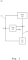
Fig. 1 , a first exemplary embodiment of thesystem 100 according to the first aspect of the invention is illustrated. Thesystem 100 may control one or more parameters of aninverter 101. It should be noted that thesystem 100 may comprise theinverter 101 or may act as a stand-alone system operably connected to theinverter 101. - For example, the
inverter 101 may correspond to any inverter-based blocks, especially to any inverter-based blocks, such as LNTA, TIAs, LPF, of an RF receiver. For instance, theinverter 101 may comprise one or more FDSOI transistors, especially one FDSOI PMOS transistor and one FDSOI NMOS transistor arranged in a complementary manner. - For example, the
system 100 may comprise abiasing circuit 102 connected to theinverter 101 via asupply line 104. The biasingcircuit 102 may correspond to a complementary constant-transconductance (Gm) biasing circuit, of which the operation is known in the art. The biasingcircuit 102 may provide a supply voltage Vd to theinverter 101, e.g., via thesupply line 104. The biasingcircuit 102 may comprise at least one transistor arrangement, especially comprising FDSOI transistors, which is not explicitly shown here. - In this regard, the FDSOI transistors of the biasing
circuit 102 and the FDSOI transistors of theinverter 101 may be interconnected via back gates of respective transistors, i.e., respective FDSOI PMOS transistors and respective FDSOI NMOS transistors, via abias line 105. - For example, the
system 100 may comprise acontrol circuit 103 connected to thesupply line 104 and further to thebias line 105. Thecontrol circuit 103 may continuously sense or monitor the supply voltage Vd at the supply line, and may compare the supply voltage Vd with a threshold voltage Vt. - It is to be noted that the threshold voltage Vt may be internally generated by the
control circuit 103. Alternatively, the threshold voltage Vt may be externally fed to thecontrol circuit 103, e.g., from an external signal generation unit connected to thecontrol circuit 103. - It is to be noted that, in the following, the implementation regarding back gate biasing (e.g., via a back gate bias voltage Vbg) is illustrated for the NMOS transistor of the
CMOS inverter 101 for simplicity if not explicitly mentioned otherwise. - For instance, the
control circuit 103 may provide the bias voltage Vbg to the interconnected back gates, e.g., via thebias line 105, when the supply voltage Vd becomes equal to the threshold voltage Vt. However, if the supply voltage Vd is less than the threshold voltage Vt, thecontrol circuit 103 may maintain the supply voltage Vd and may set the bias voltage Vbg to zero. - Accordingly, the
control circuit 103 may additionally feed the bias voltage Vbg to the interconnected back gates of the respective FDSOI transistors of the biasingcircuit 102 and theinverter 101 when the supply voltage Vd becomes equal to the threshold voltage Vt, while maintaining the supply voltage Vd to the FDSOI transistors of the biasingcircuit 102 and of theinverter 101. - As such, the
bias circuit 102 and thecontrol circuit 103 may collectively control the Gm range of theinverter 101, especially to increase the Gm range beyond the range limited by the supply voltage Vd, by means of the additional bias voltage Vbg at the interconnected back gates of the respective FDSOI transistors. - Furthermore, by means of the constant sensing and comparison of the supply voltage Vd with the threshold voltage Vt, the
control circuit 103 may provide an automatic control of the Gm of theinverter 101 over the extended Gm range of theinverter 101. - In
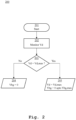
Fig. 2 , anexemplary algorithm 200 of thesystem 100 is illustrated via a process flow diagram. It is to be noted that, for simplicity, the implementation regarding the bias voltage Vbg is illustrated for the NMOS transistor of theCMOS inverter 101. - For example, during the
initiation phase 201, the biasingcircuit 102 may supply the supply voltage Vd to theinverter 101 and further to the inverter arrangement of the biasingcircuit 102, especially to ensure the proper operation of theinverter 101. Moreover, thecontrol circuit 103 may be connected to thesupply line 104 and further to thebias line 105 that may interconnect the back gates of the respective transistors of the biasingcircuit 102 and theinverter 101. - During the
monitoring phase 202, which may run along theinitiation phase 201, thecontrol circuit 103 may continuously monitor the supply voltage Vd with respect to the threshold voltage Vt. - During the
decision phase 203, thecontrol circuit 103 may sense whether the supply voltage Vd is less than the threshold voltage Vt or is equal to the threshold voltage Vt. - If the supply voltage Vd is less than the threshold voltage Vt, the
control circuit 103 may only maintain the supply voltage Vd by setting the bias voltage Vbg to zero, thereby resulting aphase 204 of the process flow. - However, if the supply voltage Vd becomes equal to the threshold voltage Vt, the control circuit may maintain the supply voltage Vd and may additionally supply the bias voltage Vbg to the interconnected back gates of the respective transistors, thereby resulting an
alternative phase 205 of the process flow. - Therefore, the process flow diagram may result in the following use case scenario in order to maintain a constant transconductance over temperature and supply voltage variations:
- a) from the
flow 203 to theflow 204, i.e., if the supply voltage Vd is less than the threshold voltage Vt, a constant Gm of theCMOS inverter 101 may be maintained by solely controlling the supply voltage Vd to theCMOS inverter 101 by setting the bias voltage Vbg=0, and - b) from the
flow 203 to theflow 205, i.e., if the supply voltage Vd is equal or greater than the threshold voltage Vt, the bias voltage Vbg may be supplied to the interconnected back gates and may be controlled accordingly to maintain a constant Gm of theCMOS inverter 101. - Additionally, the process flow from 203 to 205 may be used for a further scenario that may require an inverter with a Gm, which is higher than the Gm range solely provided by the supply voltage Vd of the inverter.
- In
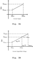
Fig. 3A , an exemplary relationship between the Gm and the supply of CMOS inverters is illustrated, where the Gm is especially controlled by a conventional complementary constant-Gm biasing circuit. - In particular, the complementary constant-Gm biasing circuit may control the inverter supply voltage such that the Gm of the inverter is inversely proportional to a control resistor of the complementary constant-Gm biasing circuit. Since the resistor value is well known across supply voltage and temperature, the Gm of the inverter can be controlled over the GM range and further maintained constant at a desired GM value by adjusting the resistance value of the control resistor which in turns adjusts the inverter supply accordingly.
- Generally, the Gm of the inverter can be expressed as the ratio of the output current to the input voltage of the inverter. In order to achieve a reliable performance, the Gm should be regulated over supply voltage and temperature variation. The control resistor of the complementary constant-Gm biasing circuit may vary the inverter supply in order to determine the Gm of the inverter, where the input and output nodes of the inverter may be unaffected in order not to disturb the signal flow.
- Since the control resistor may control the supply voltage of the inverter in order to control the Gm of the inverter, where the Gm may be limited by the inverter supply voltage as well.
- Turning back to
Fig. 3A , the horizontal axis denotes the inverter supply voltage and the vertical axis denotes the Gm. As it can be seen, the lower side of the Gm, i.e., the Gmmin, is limited by the minimum inverter supply Vdmin in order to satisfy the minimum linearity criteria of for the inverter, whereby the upper side of the Gm, i.e., the Gmmax, is limited by the maximum inverter supply Vdmax. In a conventional setup, the complementary constant-Gm biasing circuit stops being operational after reaching Vdmax. - In
Fig. 3B , an exemplary relationship between the Gm and the supply of theinverter 101 is illustrated according to the first aspect of the invention. In order to overcome the limitation of Vdmax on the upper side of the Gm, the back gates of the respective transistors of the biasingcircuit 102 and theinverter 101 may be interconnected and may be fed with the bias voltage Vbg by thecontrol circuit 103, thereby extending the inverter supply voltage range. - In
Fig. 3B , the horizontal axis denotes the inverter supply voltage Vd and the bias voltage Vbg. The vertical axis denotes the Gm of theinverter 101. It can be seen that, similar toFig. 3A , the lower side of the Gm, i.e., the Gmmin, is limited is limited by the minimum inverter supply Vdmin in order to satisfy the minimum linearity criteria of for theinverter 101, however, the upper side of the Gm in relation toFig. 3A , i.e., the Gmmax, is now extended further to Gmgreat, especially due to the application of the bias voltage Vbg to the interconnected back gates while maintaining the supply voltage Vd. - In this regard, as previously described in relation to
Fig. 1 andFig. 2 , the biasingcircuit 102 may provide the supply voltage Vd to theinverter 101 and thecontrol circuit 103 may continuously sense the supply voltage Vd with respect to the threshold voltage Vt, which is shown here as the maximum inverter supply Vdmax. - In this regard, the
control circuit 103 may exclusively maintain the supply voltage Vd to theinverter 101 over the range Vdmin to Vdmax, especially by setting the bias voltage Vbg at the interconnected back gates to zero. When the supply voltage Vd reaches to its highest limit Vdmax, thecontrol circuit 103 may apply the bias voltage Vbg to the interconnected back gates while maintaining the supply voltage Vd at its maximum limit Vdmax. - Accordingly, the Gm of the
inverter 101 can be effectively increased from the maximum limit Gmmax ofFig. 3A to a greater limit Gmgreat while simultaneously extending the inverter supply from the maximum limit Vdmax ofFig. 3A to a greater limit Vdmax, which may correspond to the supply voltage of the biasingcircuit 102. - It is to be noted that, for simplicity, the increase in the bias voltage Vbg is illustrated for the NMOS transistor of the
CMOS inverter 101. It is further to be noted that the linear relationship between the Gm and inverter supply, as shown inFig. 3A and Fig 3B , are shown only for illustration purpose, and the relationship, e.g., the curve, may be of higher order polynomial. - In
Fig. 4 , a second exemplary embodiment of thesystem 400 according to the first aspect of the invention is illustrated. In particular, thesystem 400 exemplarily shows the internal circuital arrangement of thesystem 100. - For example, the
inverter 101 may comprise the complementary FDSOI NMOS M1 and PMOS M2, where Vi may denote the input voltage and iout may denote the output voltage of theinverter 101. As such, the Gm of theinverter 101 can be expressed as:

- For a given W/L of the transistors of the
inverter 101, the Gm can be expressed as a function of the inverter supply voltage Vd. - The biasing
circuit 102 may correspond to a conventional complementary constant-Gm biasing circuit, where the back gates of the respective transistors of the biasingcircuit 102 and theinverter 101 are additionally interconnected. - For example, the biasing
circuit 102 may regulate the inverter supply voltage Vd such that the Gm of theinverter 101 can be maintained constant. Generally, the biasingcircuit 102 may comprise a start-up segment, a current mirror segment, and a control segment. - For instance, the start-up segment of the biasing
circuit 102 may comprise a PMOS M12, which may act as the start-up or regulator for thebiasing circuit 102 in order to avoid the lower values of the supply vdd of the biasingcircuit 102, especially to avoid feeding the lower values of supply voltage Vd to theinverter 101. In addition, the PMOS M12 may enter in triode region for the upper values of the supply voltage Vd to theinverter 101, thereby limiting the inverter supply voltage Vd to Vd,max. - For example, the current mirror segment may comprise any CMOS current mirror arrangement known in the art. For instance, the current mirror branches of the biasing
circuit 102 may comprise complementary pairs of PMOS M8 and NMOS M11, and PMOS M10 and NMOS M13 in order to replicate the current from one branch to the other branch. - For example, the control segment of the biasing
circuit 102 may comprise a first CMOS block comprising PMOS M4, NMOS M3, and NMOS M7, where the CMOS M3 and M4 pair may be a scaled version of the CMOS M1 and M2 pair of theinverter 101. Additionally, the control segment of the biasingcircuit 102 may comprise a second CMOS block comprising PMOS M6, NMOS M5, and NMOS M9, where the CMOS M5 and M6 pair may be a scaled version of the CMOS M1 and M2 pair of theinverter 101. - The term scaled version should be understood as having a proportional W/L ratio of the transistors. Moreover, the first CMOS block and the second CMOS block may be connected to the respective current mirror branches of the biasing
circuit 102. - In this regard, the first CMOS block or the second CMOS block may provide the resistive control for controlling the Gm of the
inverter 101. In this example, the source terminals of the PMOS m6, the NMOS M5, and the NMOS M9 are connected to the respective supply via a variable or tunable resistor R. - For example, the respective back gates of the transistors of the first CMOS block, the second CMOS block, and the
inverter 101 may be interconnected. For instance, the back gates of the PMOS M4, the PMOS M6, and the PMOS M2 may be interconnected. Additionally, the back gates of the NMOS M3, the NMOS M5, the NMOS M7, the NMOS M9, and the NMOS M1 may be interconnected. - For example, the
control circuit 103 may comprise or be anOPAMP 401. The non-inverting terminal of theOPAMP 401 may be connected to the inverter supply Vd and the inverting terminal of theOPAMP 401 may be supplied with a reference voltage, namely the threshold voltage Vd,max, such that theOPAMP 401 may compare the supply voltage Vd with the threshold voltage Vd,max. - For instance, the inverting output of the
OPAMP 401 may be connected to the interconnected back gates of the PMOS transistors, namely the back gates of the PMOS M2, the PMOS M4, and the PMOS M6. Additionally, the non-inverting output of theOPAMP 401 may be connected to the interconnected back gates of the NMOS transistors, namely the back gates of the NMOS M1, the NMOS M3, the NMOS M5, the NMOS M7, and the NMOS M9. - In this regard, the Gm of the CMOS M3/M4 can be expressed as:

- Since the CMOS M3/M4 may be a scaled version of the CMOS M1/M2 of the
inverter 101, the Gm of the CMOS M1/M2 can be expressed as:
- Accordingly, the resistor R can be varied in order to regulate or to control the G m,12 , and the resistor R is constant across temperature and supply voltage variations.
- In order to regulate the Gm range as well as the supply voltage range of the
inverter 101, theOPAMP 401 may continuously sense the supply voltage Vd with respect to the threshold voltage Vd,max. If the supply voltage Vd is less than the threshold voltage Vd,max, theOPAMP 401 may only maintain the supply voltage Vd for the CMOS transistors by disabling the bias voltage to the respective interconnected back gates of the CMOS transistors. - For instance, the
OPAMP 401 may set the bias voltage VBP to vdd for the interconnected back gates of the PMOS transistors, namely the back gates of the PMOS M2, the PMOS M4, and the PMOS M6, and may set the bias voltage VBN to zero for the interconnected back gates of the NMOS transistors, namely the back gates of the NMOS M1, the NMOS M3, the NMOS M5, the NMOS M7, and the NMOS M9. - For example, if the supply voltage Vd is greater than the threshold voltage Vd,max, the
OPAMP 401 may maintain the respective supply voltage for the CMOS transistors, whereby additionally feeding the bias voltage to the respective interconnected back gates of the CMOS transistors. - For instance, the
OPAMP 401 may set the bias voltage VBP to zero for the interconnected back gates of the PMOS transistors, namely the back gates of the PMOS M2, the PMOS M4, and the PMOS M6, and may set the bias voltage VBN to vdd for the interconnected back gates of the NMOS transistors, namely the back gates of the NMOS M1, the NMOS M3, the NMOS M5, the NMOS M7, and the NMOS M9, especially to maintain the PMOS M12 in the saturation region. - The following table exemplarily illustrates the voltage transitions for the bias voltage applied at the interconnected back gates pf the CMOS transistors.
Vd VBP VBN <Vd,max vdd 0 Slightly more than Vd,max Transition from vdd to 0 Transition from 0 to vdd >Vd, max 0 vdd - Accordingly, both the
control circuit 103 and biasingcircuit 102 may together increase the tuning range of the G m,12 of theinverter 101, whereby simultaneously providing the automatic tuning of the G m,12 of theinverter 101. - In
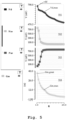
Fig. 5 , an exemplary tuning effect of the resistor R on the parameters of theCMOS inverter 101 is illustrated. Theplot 501 illustrates the variation of the inverter supply voltage Vd with the tuning of the resistor R, theplot 502 illustrates the variation of the NMOS back gate bias voltage VBN with the tuning of the resistor R, theplot 503 illustrates the variation of the PMOS back gate bias voltage VBP with the tuning of the resistor R, and finally theplot 504 illustrates the variation of the Gm of theinverter 101 with the tuning of the resistor R. - In the plots 501-504, the voltages are shown in millivolt (mV), the Gm is shown in millisiemens (mS), and the resistance is shown in ohm.
- It can be seen that above about 10mS, Vd reaches Vd,max. Therefore, in this example and in relation to
Fig. 3B , the Gm,max of theinverter 101 is about 10mS. However, due to the application of the bias voltage to the interconnected back gates of the transistors, the maximum possible supply voltage range of the inverter is extended to vdd, i.e., the supply of the biasing circuit, and the Gm range of theinverter 101 is extended to about 35mS. Accordingly, in this example and in relation toFig. 3B , the vbg,max is the vdd and the Gm,great is about 35mS. - Furthermore, the transition for the back gate bias voltage VBN from vdd to 0 at the interconnected NMOS transistors is shown in the
plot 502. Moreover, the transition for the back gate bias voltage VBp from 0 to vdd at the interconnected PMOS transistors is shown in theplot 503. - As such, the previous Gm tuning range of 2mS to 10mS of the
inverter 101 is successfully extended to achieve a wider Gm tuning range of 2mS to greater than 30mS. - In
Fig. 6 , an exemplary embodiment of themethod 600 according to the second aspect of the invention is illustrated. In afirst step 601, a supply voltage is provided to a CMOS inverter by a biasing circuit, where at least one transistor arrangement of the biasing circuit and the CMOS inverter are interconnected via back gates of respective transistors. - In a
second step 602, a bias voltage is provided to the interconnected back gates by a control circuit when the supply voltage reaches to a threshold value. In athird step 603, the transconductance of the CMOS inverter is controlled together by the biasing circuit and the control circuit. - It is important to note that, in the description as well as in the claims, the word "comprising" does not exclude other elements or steps and the indefinite article "a" or "an" does not exclude a plurality. A single element or other unit may fulfill the functions of several entities or items recited in the claims.
- It should be understood that the term "and/or" used in the specification and the appended claims of this application refers to any combination and all possible combinations of one or more associated listed items, and includes these combinations.
- It should also be understood that the word "connected" implies that the elements may be directly connected together or may be coupled through one or more intervening elements. Moreover, the disclosure with regard to any of the aspects is also relevant with regard to the other aspects of the disclosure.
- Although the invention has been illustrated and described with respect to one or more implementations, equivalent alterations and modifications will occur to others skilled in the art upon the reading and understanding of this specification and the annexed drawings. In addition, while a particular feature of the invention may have been disclosed with respect to only one of several implementations, such feature may be combined with one or more other features of the other implementations as may be desired and advantageous for any given or particular application.
Claims (15)
- A system (100) for increasing the transconductance of a Complementary Metal-Oxide Semiconductor, CMOS, inverter (101), the system comprises:a biasing circuit (102) configured to provide a supply voltage (Vd) to the CMOS inverter (101), wherein the biasing circuit (102) comprises at least one transistor arrangement, wherein the transistor arrangement and the CMOS inverter (101) are interconnected via back gates of respective transistors, anda control circuit (103) configured to provide a bias voltage (Vbg) to the interconnected back gates when the supply voltage (Vd) reaches to a threshold value (Vt), whereby both the biasing circuit (102) and the control circuit (103) together control the transconductance of the CMOS inverter (101).
- The system according to claim 1,
wherein the control circuit (103) is further configured to maintain the supply voltage (Vd) to the CMOS inverter (101) when the supply voltage (Vd) is higher than the threshold value (Vt). - The system according to claim 1 or 2,wherein the transistor arrangement comprises at least one replicated CMOS inverter (M3, M4, M5, M6) corresponding to a scaled version of the CMOS inverter (101) and at least one resistor (R), especially a tunable resistor, operably connected to the replicated CMOS inverter (M3, M4, M5, M6), andwherein the transistor arrangement is configured to control the transconductance of the CMOS inverter (101) by means of the replicated CMOS inverter (M3, M4, M5, M6) and the resistor (R) .
- The system according to any of claims 1 to 3,
wherein the biasing circuit (102) is configured to provide the supply voltage (Vd) ranging from a predefined minimum value to the threshold value (Vt). - The system according to claim 4,wherein the predefined minimum value is defined based on a minimum linearity criteria of the transconductance of the CMOS inverter (101), and/orwherein the threshold value (Vt) is defined based on an operation criteria of the transistor arrangement.
- The system according to claim 4 or 5,wherein the transistor arrangement of the biasing circuit (102) is configured to control the transconductance of the CMOS inverter (101) for the supply voltage (Vd) ranging from the predefined minimum value to the threshold value (Vt), andwherein the transconductance is inversely proportional to the resistor (R) of the transistor arrangement.
- The system according to any of claims 1 to 6,
wherein the control circuit (103) is configured to provide the bias voltage (Vbg) to the interconnected back gates ranging from zero to a supply voltage of the biasing circuit (103) . - The system according to claim 7,
wherein the transistor arrangement of the biasing circuit (102) is configured to control the transconductance of the CMOS inverter (101) for the bias voltage (Vbg) to the interconnected back gates ranging from zero to the supply voltage of the biasing circuit (103). - The system according to any of claims 1 to 8,
wherein the control circuit (103) comprises at least one comparator (401), preferably an operational amplifier comparator, configured to sense the supply voltage (Vd) from the biasing circuit (102) and further to compare the supply voltage (Vd) with the threshold value (Vt). - The system according to claim 9,
wherein the comparator (401) is further configured to exclusively feed the supply voltage (Vd) to the transistor arrangement and the CMOS inverter (101) when the supply voltage (Vd) is lower than the threshold value (Vt) and to additionally feed the bias voltage (Vbg) to the interconnected back gates of the respective transistors of the transistor arrangement and the CMOS inverter (101) when the supply voltage (Vd) reaches to the threshold value (Vt). - The system according to any of claims 1 to 10,
wherein the respective transistors of the transistor arrangement and the CMOS inverter (101) are Fully-Depleted Silicon-on-Insulator, FDSOI, transistors. - A method (600) for increasing the transconductance of a complementary metal oxide semiconductor, CMOS, inverter, the method comprises:providing (601), by a biasing circuit, a supply voltage to the CMOS inverter, wherein at least one transistor arrangement of the biasing circuit and the CMOS inverter are interconnected via back gates of respective transistors,providing (602), by a control circuit, a bias voltage to the interconnected back gates when the supply voltage reaches to a threshold value, andcontrolling (603), together by the biasing circuit and the control circuit, the transconductance of the CMOS inverter.
- The method according to claim 12,
wherein the method further comprises maintaining, by the control circuit, the supply voltage to the CMOS inverter when the supply voltage is higher than the threshold value. - The method according to claim 12 or 13,
wherein the method further comprises:providing, by the biasing circuit, the supply voltage ranging from a predefined minimum value to the threshold value, andproviding, by the control circuit, the bias voltage to the interconnected back gates ranging from zero to a supply voltage of the biasing circuit. - The method according to claim 14,
wherein the method further comprises:controlling, by the transistor arrangement, the transconductance of the CMOS inverter for the supply voltage ranging from the predefined minimum value to the threshold value, andcontrolling, by the transistor arrangement, the transconductance of the CMOS inverter for the bias voltage to the interconnected back gates ranging from zero to the supply voltage of the biasing circuit.
Priority Applications (2)
| Application Number | Priority Date | Filing Date | Title |
|---|---|---|---|
| EP23219084.3A EP4576568A1 (en) | 2023-12-21 | 2023-12-21 | System and method for increasing transconductance of a cmos inverter |
| US18/976,600 US20250211233A1 (en) | 2023-12-21 | 2024-12-11 | System and method for increasing transconductance of a cmos inverter |
Applications Claiming Priority (1)
| Application Number | Priority Date | Filing Date | Title |
|---|---|---|---|
| EP23219084.3A EP4576568A1 (en) | 2023-12-21 | 2023-12-21 | System and method for increasing transconductance of a cmos inverter |
Publications (1)
| Publication Number | Publication Date |
|---|---|
| EP4576568A1 true EP4576568A1 (en) | 2025-06-25 |
Family
ID=89430496
Family Applications (1)
| Application Number | Title | Priority Date | Filing Date |
|---|---|---|---|
| EP23219084.3A Pending EP4576568A1 (en) | 2023-12-21 | 2023-12-21 | System and method for increasing transconductance of a cmos inverter |
Country Status (2)
| Country | Link |
|---|---|
| US (1) | US20250211233A1 (en) |
| EP (1) | EP4576568A1 (en) |
Citations (2)
| Publication number | Priority date | Publication date | Assignee | Title |
|---|---|---|---|---|
| US20080218265A1 (en) * | 2007-03-09 | 2008-09-11 | Analog Devices, Inc. | Amplifier structures that enhance transient currents and signal swing |
| US20170324385A1 (en) * | 2016-05-06 | 2017-11-09 | Globalfoundries Inc. | Method, apparatus and system for back gate biasing for fd-soi devices |
Family Cites Families (2)
| Publication number | Priority date | Publication date | Assignee | Title |
|---|---|---|---|---|
| JP5404473B2 (en) * | 2010-02-26 | 2014-01-29 | ルネサスエレクトロニクス株式会社 | High frequency power amplifier and operation method thereof |
| US10020782B2 (en) * | 2015-10-08 | 2018-07-10 | Dsp Group Ltd. | PVT robust closed loop CMOS bias for linear power amplifier |
-
2023
- 2023-12-21 EP EP23219084.3A patent/EP4576568A1/en active Pending
-
2024
- 2024-12-11 US US18/976,600 patent/US20250211233A1/en active Pending
Patent Citations (2)
| Publication number | Priority date | Publication date | Assignee | Title |
|---|---|---|---|---|
| US20080218265A1 (en) * | 2007-03-09 | 2008-09-11 | Analog Devices, Inc. | Amplifier structures that enhance transient currents and signal swing |
| US20170324385A1 (en) * | 2016-05-06 | 2017-11-09 | Globalfoundries Inc. | Method, apparatus and system for back gate biasing for fd-soi devices |
Non-Patent Citations (2)
| Title |
|---|
| JANSEN ET AL.: "Complementary constant-gm biasing of Nauta-transconductors in low-power Gm-C filters to +/-2% accuracy over temperature", PROCEEDINGS OF THE ESSCIRC, 2012, pages 466 - 469 |
| YUSUKE TSUGITA ET AL: "An On-Chip PVT Compensation Technique with Current Monitoring Circuit for Low-Voltage CMOS Digital LSIs", IEICE TRANSACTIONS ON ELECTRONICS, INSTITUTE OF ELECTRONICS, TOKYO, JP, vol. E93C, no. 6, 1 June 2010 (2010-06-01), pages 835 - 841, XP001557247, ISSN: 0916-8524, DOI: 10.1587/TRANSELE.E93.C.835 * |
Also Published As
| Publication number | Publication date |
|---|---|
| US20250211233A1 (en) | 2025-06-26 |
Similar Documents
| Publication | Publication Date | Title |
|---|---|---|
| US8854023B2 (en) | Low dropout linear regulator | |
| TWI480714B (en) | Voltage regulator | |
| US20060055383A1 (en) | Adaptive biasing concept for current mode voltage regulators | |
| US4050030A (en) | Offset adjustment circuit | |
| US6717471B2 (en) | Automatic gain adjustment circuit and amplifier using the same | |
| GB2263597A (en) | Bias current source for a mixed pnp-npn amplifier | |
| EP4385127A1 (en) | Variable gain amplifier with temperature compensated gain | |
| US7323935B2 (en) | Transconductance amplifier having common mode feedback circuit and method of operating the transconductance amplifier | |
| US7068090B2 (en) | Amplifier circuit | |
| US5455539A (en) | Device for regulating the common mode voltage at the output of a balanced amplifier | |
| US9729126B2 (en) | Method and implementation for accurate gain-bandwidth product tuning | |
| EP0957578B1 (en) | Transconductance control circuit, particularly for continous-time circuits | |
| US6985038B2 (en) | Operational amplifier generating desired feedback reference voltage allowing improved output characteristic | |
| EP1213724B1 (en) | Process-insensitive, highly-linear constant transconductance circuit | |
| US20250211233A1 (en) | System and method for increasing transconductance of a cmos inverter | |
| US5994926A (en) | Circuit and method for programmably changing the transconductance of a transconductor circuit | |
| US20040104746A1 (en) | Transconductance varying circuit of transconductor circuit, varying bandwidth filter circuit using the same and digital tuning circuit of transconductor-capacitor filter | |
| US7199685B2 (en) | Three-terminal, tunable active inductor | |
| US11012041B2 (en) | Differential amplifier circuit | |
| US12537490B2 (en) | Amplifier and method for controlling common mode voltage of the same | |
| JP5646166B2 (en) | Power circuit | |
| US6933773B2 (en) | Integrated circuit | |
| US7446608B2 (en) | Variable gain amplifier with constant input referred third order intercept | |
| WO2022234122A1 (en) | Signal processing | |
| US12597915B2 (en) | Capacitance circuit |
Legal Events
| Date | Code | Title | Description |
|---|---|---|---|
| PUAI | Public reference made under article 153(3) epc to a published international application that has entered the european phase |
Free format text: ORIGINAL CODE: 0009012 |
|
| STAA | Information on the status of an ep patent application or granted ep patent |
Free format text: STATUS: THE APPLICATION HAS BEEN PUBLISHED |
|
| AK | Designated contracting states |
Kind code of ref document: A1 Designated state(s): AL AT BE BG CH CY CZ DE DK EE ES FI FR GB GR HR HU IE IS IT LI LT LU LV MC ME MK MT NL NO PL PT RO RS SE SI SK SM TR |
|
| STAA | Information on the status of an ep patent application or granted ep patent |
Free format text: STATUS: REQUEST FOR EXAMINATION WAS MADE |
|
| 17P | Request for examination filed |
Effective date: 20251127 |