EP4576529A1 - Power supply system - Google Patents
Power supply system Download PDFInfo
- Publication number
- EP4576529A1 EP4576529A1 EP24219844.8A EP24219844A EP4576529A1 EP 4576529 A1 EP4576529 A1 EP 4576529A1 EP 24219844 A EP24219844 A EP 24219844A EP 4576529 A1 EP4576529 A1 EP 4576529A1
- Authority
- EP
- European Patent Office
- Prior art keywords
- circuit
- voltage
- power supply
- supply system
- isolated
- Prior art date
- Legal status (The legal status is an assumption and is not a legal conclusion. Google has not performed a legal analysis and makes no representation as to the accuracy of the status listed.)
- Pending
Links
Images


Classifications
-
- H—ELECTRICITY
- H02—GENERATION; CONVERSION OR DISTRIBUTION OF ELECTRIC POWER
- H02M—APPARATUS FOR CONVERSION BETWEEN AC AND AC, BETWEEN AC AND DC, OR BETWEEN DC AND DC, AND FOR USE WITH MAINS OR SIMILAR POWER SUPPLY SYSTEMS; CONVERSION OF DC OR AC INPUT POWER INTO SURGE OUTPUT POWER; CONTROL OR REGULATION THEREOF
- H02M7/00—Conversion of AC power input into DC power output; Conversion of DC power input into AC power output
- H02M7/02—Conversion of AC power input into DC power output without possibility of reversal
- H02M7/04—Conversion of AC power input into DC power output without possibility of reversal by static converters
- H02M7/12—Conversion of AC power input into DC power output without possibility of reversal by static converters using discharge tubes with control electrode or semiconductor devices with control electrode
- H02M7/21—Conversion of AC power input into DC power output without possibility of reversal by static converters using discharge tubes with control electrode or semiconductor devices with control electrode using devices of a triode or transistor type requiring continuous application of a control signal
- H02M7/217—Conversion of AC power input into DC power output without possibility of reversal by static converters using discharge tubes with control electrode or semiconductor devices with control electrode using devices of a triode or transistor type requiring continuous application of a control signal using semiconductor devices only
- H02M7/219—Conversion of AC power input into DC power output without possibility of reversal by static converters using discharge tubes with control electrode or semiconductor devices with control electrode using devices of a triode or transistor type requiring continuous application of a control signal using semiconductor devices only in a bridge configuration
-
- H—ELECTRICITY
- H02—GENERATION; CONVERSION OR DISTRIBUTION OF ELECTRIC POWER
- H02M—APPARATUS FOR CONVERSION BETWEEN AC AND AC, BETWEEN AC AND DC, OR BETWEEN DC AND DC, AND FOR USE WITH MAINS OR SIMILAR POWER SUPPLY SYSTEMS; CONVERSION OF DC OR AC INPUT POWER INTO SURGE OUTPUT POWER; CONTROL OR REGULATION THEREOF
- H02M1/00—Details of apparatus for conversion
- H02M1/0067—Converter structures employing plural converter units, other than for parallel operation of the units on a single load
- H02M1/007—Plural converter units in cascade
-
- H—ELECTRICITY
- H02—GENERATION; CONVERSION OR DISTRIBUTION OF ELECTRIC POWER
- H02J—ELECTRIC POWER NETWORKS; CIRCUIT ARRANGEMENTS OR SYSTEMS FOR SUPPLYING OR DISTRIBUTING ELECTRIC POWER; SYSTEMS FOR STORING ELECTRIC ENERGY
- H02J7/00—Circuit arrangements for charging or discharging batteries or for supplying loads from batteries
- H02J7/855—Circuit arrangements for charging or discharging batteries or for supplying loads from batteries with circuits adapted for supplying loads from the battery
-
- H—ELECTRICITY
- H02—GENERATION; CONVERSION OR DISTRIBUTION OF ELECTRIC POWER
- H02J—ELECTRIC POWER NETWORKS; CIRCUIT ARRANGEMENTS OR SYSTEMS FOR SUPPLYING OR DISTRIBUTING ELECTRIC POWER; SYSTEMS FOR STORING ELECTRIC ENERGY
- H02J9/00—Circuit arrangements for emergency or stand-by power supply, e.g. for emergency lighting
- H02J9/04—Circuit arrangements for emergency or stand-by power supply, e.g. for emergency lighting in which the distribution system is disconnected from the normal source and connected to a standby source
- H02J9/06—Circuit arrangements for emergency or stand-by power supply, e.g. for emergency lighting in which the distribution system is disconnected from the normal source and connected to a standby source with automatic change-over, e.g. UPS systems
- H02J9/061—Circuit arrangements for emergency or stand-by power supply, e.g. for emergency lighting in which the distribution system is disconnected from the normal source and connected to a standby source with automatic change-over, e.g. UPS systems for DC powered loads
-
- H—ELECTRICITY
- H02—GENERATION; CONVERSION OR DISTRIBUTION OF ELECTRIC POWER
- H02M—APPARATUS FOR CONVERSION BETWEEN AC AND AC, BETWEEN AC AND DC, OR BETWEEN DC AND DC, AND FOR USE WITH MAINS OR SIMILAR POWER SUPPLY SYSTEMS; CONVERSION OF DC OR AC INPUT POWER INTO SURGE OUTPUT POWER; CONTROL OR REGULATION THEREOF
- H02M1/00—Details of apparatus for conversion
- H02M1/0048—Circuits or arrangements for reducing losses
- H02M1/0054—Transistor switching losses
- H02M1/0058—Transistor switching losses by employing soft switching techniques, i.e. commutation of transistors when applied voltage is zero or when current flow is zero
-
- H—ELECTRICITY
- H02—GENERATION; CONVERSION OR DISTRIBUTION OF ELECTRIC POWER
- H02M—APPARATUS FOR CONVERSION BETWEEN AC AND AC, BETWEEN AC AND DC, OR BETWEEN DC AND DC, AND FOR USE WITH MAINS OR SIMILAR POWER SUPPLY SYSTEMS; CONVERSION OF DC OR AC INPUT POWER INTO SURGE OUTPUT POWER; CONTROL OR REGULATION THEREOF
- H02M1/00—Details of apparatus for conversion
- H02M1/0067—Converter structures employing plural converter units, other than for parallel operation of the units on a single load
- H02M1/0074—Plural converter units whose inputs are connected in series
-
- H—ELECTRICITY
- H02—GENERATION; CONVERSION OR DISTRIBUTION OF ELECTRIC POWER
- H02M—APPARATUS FOR CONVERSION BETWEEN AC AND AC, BETWEEN AC AND DC, OR BETWEEN DC AND DC, AND FOR USE WITH MAINS OR SIMILAR POWER SUPPLY SYSTEMS; CONVERSION OF DC OR AC INPUT POWER INTO SURGE OUTPUT POWER; CONTROL OR REGULATION THEREOF
- H02M1/00—Details of apparatus for conversion
- H02M1/14—Arrangements for reducing ripples from DC input or output
-
- H—ELECTRICITY
- H02—GENERATION; CONVERSION OR DISTRIBUTION OF ELECTRIC POWER
- H02M—APPARATUS FOR CONVERSION BETWEEN AC AND AC, BETWEEN AC AND DC, OR BETWEEN DC AND DC, AND FOR USE WITH MAINS OR SIMILAR POWER SUPPLY SYSTEMS; CONVERSION OF DC OR AC INPUT POWER INTO SURGE OUTPUT POWER; CONTROL OR REGULATION THEREOF
- H02M1/00—Details of apparatus for conversion
- H02M1/44—Circuits or arrangements for compensating for electromagnetic interference in converters or inverters
-
- H—ELECTRICITY
- H02—GENERATION; CONVERSION OR DISTRIBUTION OF ELECTRIC POWER
- H02M—APPARATUS FOR CONVERSION BETWEEN AC AND AC, BETWEEN AC AND DC, OR BETWEEN DC AND DC, AND FOR USE WITH MAINS OR SIMILAR POWER SUPPLY SYSTEMS; CONVERSION OF DC OR AC INPUT POWER INTO SURGE OUTPUT POWER; CONTROL OR REGULATION THEREOF
- H02M3/00—Conversion of DC power input into DC power output
- H02M3/01—Resonant DC/DC converters
-
- H—ELECTRICITY
- H02—GENERATION; CONVERSION OR DISTRIBUTION OF ELECTRIC POWER
- H02M—APPARATUS FOR CONVERSION BETWEEN AC AND AC, BETWEEN AC AND DC, OR BETWEEN DC AND DC, AND FOR USE WITH MAINS OR SIMILAR POWER SUPPLY SYSTEMS; CONVERSION OF DC OR AC INPUT POWER INTO SURGE OUTPUT POWER; CONTROL OR REGULATION THEREOF
- H02M3/00—Conversion of DC power input into DC power output
- H02M3/22—Conversion of DC power input into DC power output with intermediate conversion into AC
- H02M3/24—Conversion of DC power input into DC power output with intermediate conversion into AC by static converters
- H02M3/28—Conversion of DC power input into DC power output with intermediate conversion into AC by static converters using discharge tubes with control electrode or semiconductor devices with control electrode to produce the intermediate AC
- H02M3/325—Conversion of DC power input into DC power output with intermediate conversion into AC by static converters using discharge tubes with control electrode or semiconductor devices with control electrode to produce the intermediate AC using devices of a triode or a transistor type requiring continuous application of a control signal
- H02M3/335—Conversion of DC power input into DC power output with intermediate conversion into AC by static converters using discharge tubes with control electrode or semiconductor devices with control electrode to produce the intermediate AC using devices of a triode or a transistor type requiring continuous application of a control signal using semiconductor devices only
- H02M3/33569—Conversion of DC power input into DC power output with intermediate conversion into AC by static converters using discharge tubes with control electrode or semiconductor devices with control electrode to produce the intermediate AC using devices of a triode or a transistor type requiring continuous application of a control signal using semiconductor devices only having several active switching elements
- H02M3/33571—Half-bridge at primary side of an isolation transformer
-
- H—ELECTRICITY
- H02—GENERATION; CONVERSION OR DISTRIBUTION OF ELECTRIC POWER
- H02M—APPARATUS FOR CONVERSION BETWEEN AC AND AC, BETWEEN AC AND DC, OR BETWEEN DC AND DC, AND FOR USE WITH MAINS OR SIMILAR POWER SUPPLY SYSTEMS; CONVERSION OF DC OR AC INPUT POWER INTO SURGE OUTPUT POWER; CONTROL OR REGULATION THEREOF
- H02M3/00—Conversion of DC power input into DC power output
- H02M3/22—Conversion of DC power input into DC power output with intermediate conversion into AC
- H02M3/24—Conversion of DC power input into DC power output with intermediate conversion into AC by static converters
- H02M3/28—Conversion of DC power input into DC power output with intermediate conversion into AC by static converters using discharge tubes with control electrode or semiconductor devices with control electrode to produce the intermediate AC
- H02M3/325—Conversion of DC power input into DC power output with intermediate conversion into AC by static converters using discharge tubes with control electrode or semiconductor devices with control electrode to produce the intermediate AC using devices of a triode or a transistor type requiring continuous application of a control signal
- H02M3/335—Conversion of DC power input into DC power output with intermediate conversion into AC by static converters using discharge tubes with control electrode or semiconductor devices with control electrode to produce the intermediate AC using devices of a triode or a transistor type requiring continuous application of a control signal using semiconductor devices only
- H02M3/33569—Conversion of DC power input into DC power output with intermediate conversion into AC by static converters using discharge tubes with control electrode or semiconductor devices with control electrode to produce the intermediate AC using devices of a triode or a transistor type requiring continuous application of a control signal using semiconductor devices only having several active switching elements
- H02M3/33573—Full-bridge at primary side of an isolation transformer
-
- H—ELECTRICITY
- H02—GENERATION; CONVERSION OR DISTRIBUTION OF ELECTRIC POWER
- H02M—APPARATUS FOR CONVERSION BETWEEN AC AND AC, BETWEEN AC AND DC, OR BETWEEN DC AND DC, AND FOR USE WITH MAINS OR SIMILAR POWER SUPPLY SYSTEMS; CONVERSION OF DC OR AC INPUT POWER INTO SURGE OUTPUT POWER; CONTROL OR REGULATION THEREOF
- H02M3/00—Conversion of DC power input into DC power output
- H02M3/22—Conversion of DC power input into DC power output with intermediate conversion into AC
- H02M3/24—Conversion of DC power input into DC power output with intermediate conversion into AC by static converters
- H02M3/28—Conversion of DC power input into DC power output with intermediate conversion into AC by static converters using discharge tubes with control electrode or semiconductor devices with control electrode to produce the intermediate AC
- H02M3/325—Conversion of DC power input into DC power output with intermediate conversion into AC by static converters using discharge tubes with control electrode or semiconductor devices with control electrode to produce the intermediate AC using devices of a triode or a transistor type requiring continuous application of a control signal
- H02M3/335—Conversion of DC power input into DC power output with intermediate conversion into AC by static converters using discharge tubes with control electrode or semiconductor devices with control electrode to produce the intermediate AC using devices of a triode or a transistor type requiring continuous application of a control signal using semiconductor devices only
- H02M3/33569—Conversion of DC power input into DC power output with intermediate conversion into AC by static converters using discharge tubes with control electrode or semiconductor devices with control electrode to produce the intermediate AC using devices of a triode or a transistor type requiring continuous application of a control signal using semiconductor devices only having several active switching elements
- H02M3/33576—Conversion of DC power input into DC power output with intermediate conversion into AC by static converters using discharge tubes with control electrode or semiconductor devices with control electrode to produce the intermediate AC using devices of a triode or a transistor type requiring continuous application of a control signal using semiconductor devices only having several active switching elements having at least one active switching element at the secondary side of an isolation transformer
- H02M3/33584—Bidirectional converters
-
- H—ELECTRICITY
- H02—GENERATION; CONVERSION OR DISTRIBUTION OF ELECTRIC POWER
- H02M—APPARATUS FOR CONVERSION BETWEEN AC AND AC, BETWEEN AC AND DC, OR BETWEEN DC AND DC, AND FOR USE WITH MAINS OR SIMILAR POWER SUPPLY SYSTEMS; CONVERSION OF DC OR AC INPUT POWER INTO SURGE OUTPUT POWER; CONTROL OR REGULATION THEREOF
- H02M3/00—Conversion of DC power input into DC power output
- H02M3/22—Conversion of DC power input into DC power output with intermediate conversion into AC
- H02M3/24—Conversion of DC power input into DC power output with intermediate conversion into AC by static converters
- H02M3/28—Conversion of DC power input into DC power output with intermediate conversion into AC by static converters using discharge tubes with control electrode or semiconductor devices with control electrode to produce the intermediate AC
- H02M3/325—Conversion of DC power input into DC power output with intermediate conversion into AC by static converters using discharge tubes with control electrode or semiconductor devices with control electrode to produce the intermediate AC using devices of a triode or a transistor type requiring continuous application of a control signal
- H02M3/335—Conversion of DC power input into DC power output with intermediate conversion into AC by static converters using discharge tubes with control electrode or semiconductor devices with control electrode to produce the intermediate AC using devices of a triode or a transistor type requiring continuous application of a control signal using semiconductor devices only
- H02M3/33569—Conversion of DC power input into DC power output with intermediate conversion into AC by static converters using discharge tubes with control electrode or semiconductor devices with control electrode to produce the intermediate AC using devices of a triode or a transistor type requiring continuous application of a control signal using semiconductor devices only having several active switching elements
- H02M3/33576—Conversion of DC power input into DC power output with intermediate conversion into AC by static converters using discharge tubes with control electrode or semiconductor devices with control electrode to produce the intermediate AC using devices of a triode or a transistor type requiring continuous application of a control signal using semiconductor devices only having several active switching elements having at least one active switching element at the secondary side of an isolation transformer
- H02M3/33592—Conversion of DC power input into DC power output with intermediate conversion into AC by static converters using discharge tubes with control electrode or semiconductor devices with control electrode to produce the intermediate AC using devices of a triode or a transistor type requiring continuous application of a control signal using semiconductor devices only having several active switching elements having at least one active switching element at the secondary side of an isolation transformer having a synchronous rectifier circuit or a synchronous freewheeling circuit at the secondary side of an isolation transformer
-
- H—ELECTRICITY
- H02—GENERATION; CONVERSION OR DISTRIBUTION OF ELECTRIC POWER
- H02M—APPARATUS FOR CONVERSION BETWEEN AC AND AC, BETWEEN AC AND DC, OR BETWEEN DC AND DC, AND FOR USE WITH MAINS OR SIMILAR POWER SUPPLY SYSTEMS; CONVERSION OF DC OR AC INPUT POWER INTO SURGE OUTPUT POWER; CONTROL OR REGULATION THEREOF
- H02M7/00—Conversion of AC power input into DC power output; Conversion of DC power input into AC power output
- H02M7/02—Conversion of AC power input into DC power output without possibility of reversal
- H02M7/04—Conversion of AC power input into DC power output without possibility of reversal by static converters
- H02M7/06—Conversion of AC power input into DC power output without possibility of reversal by static converters using discharge tubes without control electrode or semiconductor devices without control electrode
- H02M7/08—Conversion of AC power input into DC power output without possibility of reversal by static converters using discharge tubes without control electrode or semiconductor devices without control electrode arranged for operation in parallel
-
- H—ELECTRICITY
- H02—GENERATION; CONVERSION OR DISTRIBUTION OF ELECTRIC POWER
- H02M—APPARATUS FOR CONVERSION BETWEEN AC AND AC, BETWEEN AC AND DC, OR BETWEEN DC AND DC, AND FOR USE WITH MAINS OR SIMILAR POWER SUPPLY SYSTEMS; CONVERSION OF DC OR AC INPUT POWER INTO SURGE OUTPUT POWER; CONTROL OR REGULATION THEREOF
- H02M7/00—Conversion of AC power input into DC power output; Conversion of DC power input into AC power output
- H02M7/42—Conversion of DC power input into AC power output without possibility of reversal
- H02M7/44—Conversion of DC power input into AC power output without possibility of reversal by static converters
- H02M7/48—Conversion of DC power input into AC power output without possibility of reversal by static converters using discharge tubes with control electrode or semiconductor devices with control electrode
- H02M7/483—Converters with outputs that each can have more than two voltages levels
- H02M7/4835—Converters with outputs that each can have more than two voltages levels comprising two or more cells, each including a switchable capacitor, the capacitors having a nominal charge voltage which corresponds to a given fraction of the input voltage, and the capacitors being selectively connected in series to determine the instantaneous output voltage
-
- H—ELECTRICITY
- H02—GENERATION; CONVERSION OR DISTRIBUTION OF ELECTRIC POWER
- H02J—ELECTRIC POWER NETWORKS; CIRCUIT ARRANGEMENTS OR SYSTEMS FOR SUPPLYING OR DISTRIBUTING ELECTRIC POWER; SYSTEMS FOR STORING ELECTRIC ENERGY
- H02J2101/00—Supply or distribution of decentralised, dispersed or local electric power generation
- H02J2101/20—Dispersed power generation using renewable energy sources
- H02J2101/22—Solar energy
-
- H—ELECTRICITY
- H02—GENERATION; CONVERSION OR DISTRIBUTION OF ELECTRIC POWER
- H02J—ELECTRIC POWER NETWORKS; CIRCUIT ARRANGEMENTS OR SYSTEMS FOR SUPPLYING OR DISTRIBUTING ELECTRIC POWER; SYSTEMS FOR STORING ELECTRIC ENERGY
- H02J2101/00—Supply or distribution of decentralised, dispersed or local electric power generation
- H02J2101/20—Dispersed power generation using renewable energy sources
- H02J2101/28—Wind energy
-
- H—ELECTRICITY
- H02—GENERATION; CONVERSION OR DISTRIBUTION OF ELECTRIC POWER
- H02J—ELECTRIC POWER NETWORKS; CIRCUIT ARRANGEMENTS OR SYSTEMS FOR SUPPLYING OR DISTRIBUTING ELECTRIC POWER; SYSTEMS FOR STORING ELECTRIC ENERGY
- H02J2101/00—Supply or distribution of decentralised, dispersed or local electric power generation
- H02J2101/20—Dispersed power generation using renewable energy sources
- H02J2101/30—Fuel cells
-
- H—ELECTRICITY
- H02—GENERATION; CONVERSION OR DISTRIBUTION OF ELECTRIC POWER
- H02J—ELECTRIC POWER NETWORKS; CIRCUIT ARRANGEMENTS OR SYSTEMS FOR SUPPLYING OR DISTRIBUTING ELECTRIC POWER; SYSTEMS FOR STORING ELECTRIC ENERGY
- H02J2105/00—Networks for supplying or distributing electric power characterised by their spatial reach or by the load
- H02J2105/40—Networks for supplying or distributing electric power characterised by their spatial reach or by the load characterised by the loads connecting to the networks or being supplied by the networks
- H02J2105/42—Home appliances
- H02J2105/425—Home appliances the loads being an Information and Communication Technology [ICT] facility
Definitions
- the present disclosure relates to a power supply system, and more particularly to a power supply system for a data center.
- Data centers are global collaborative networks of specified devices that play an important role in accelerating the transmission, computing and storage of data information. As the scale of data centers continues to expand, the required power level continues to rise. Consequently, the requirements for the efficiency of the power supply systems of the data centers gradually increase in the market.
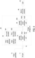
- FIG. 1 is a schematic functional block diagram illustrating a conventional power supply system for a data center.
- the data center power supply system 200 includes an AC-to-DC power conversion unit 210, a server power supply 220 and an energy storage unit 23.
- An AC grid 11 or a power generator 12 can generate AC power with a medium voltage of at least 10 kV
- the AC power is transmitted to the input terminal of the AC-to-DC power conversion unit 210 of the data center power supply system 200 through a transformer network 13.
- the AC power is converted into a first DC voltage Vdc1 by the AC-to-DC power conversion unit 210.
- the first DC voltage Vdc1 is provided to a first DC bus (bus1).
- the voltage value of the first DC voltage Vdc1 is about 240 V
- the server power supply 220 is usually equipped with a power factor correction (PFC) converter 221 and a first DC-to-DC converter 222.
- PFC power factor correction
- the server power supply 220 the first DC voltage Vdc1 on the first DC bus1 is converted to a second DC voltage Vdc2 on a second DC bus (bus2).
- the voltage value of the second DC voltage Vdc2 is usually 12V, 48V or 54V based on the requirements of a load 40.
- a second DC-to-DC converter 30' is serially connected between the load 40 and the second DC bus (bus2) to provide the voltage reduction function and the voltage regulation function.
- the energy storage unit 23 connected to the server power supply 220 is enabled to provide electric power to the server power supply 220. Consequently, the server power supply 220 can work for a certain period so that data in the servers can be backup.
- server power supply 220 includes the PFC converter 221 and the first DC-to-DC converter 222, this two-stage circuit design reduces the overall power conversion efficiency. Since number of the power conversion stages of the data center power supply system directly affects the power efficiency and reliability, it is important to provide an improved system architecture of a data center power supply system with the reduced power conversion stages.
- the present disclosure provides a power supply system for a data center.
- the power supply system is electrically connected with an AC voltage. Firstly, the AC voltage is converted into a first DC voltage by an isolated AC-to-DC power conversion unit. Then, the first DC voltage is converted into a second DC voltage by an isolated DC-to-DC power conversion unit having a relatively simple circuitry topology. Consequently, the conversion efficiency of the overall power supply system is improved.
- a power supply system includes an isolated AC-to-DC power conversion unit, an isolated DC-to-DC power conversion unit and an energy storage unit.
- the isolated AC-to-DC power conversion unit converts a system input voltage into a first DC voltage.
- the first DC voltage is provided to a first DC bus.
- the isolated DC-to-DC power conversion unit is electrically connected with the isolated AC-to-DC power conversion unit through the first DC bus.
- the first DC voltage from the first DC bus is converted into a second DC voltage by the isolated DC-to-DC power conversion unit.
- the second DC voltage is provided to a load.
- a main power circuit in the isolated DC-to-DC power conversion unit is an LLC circuit or a boost-SRC circuit.
- a voltage value of the second DC voltage is between 0.5V and 60V
- the energy storage unit includes a battery and is electrically connected with the first DC bus.
- the energy storage unit is charged to a floating charge state, and a voltage value of the first DC voltage is between 380V and 1500V
- An AC grid 11 or a power generator 12 can generate AC power with a medium voltage of at least 10 kV.
- the AC power is converted into a system input voltage for the power supply system 20.
- the system input voltage is transmitted to the input terminal of the isolated AC-to-DC power conversion unit 21.
- the system input voltage is a medium AC voltage of at least 10 kV or a low AC voltage between 400 V and 690 V.
- the isolated AC-to-DC power conversion unit 21 the system input voltage is converted into a first DC voltage Vdc1.
- the first DC voltage Vdc1 is provided to a first DC bus (bus1).
- the isolated AC-to-DC power conversion unit 21 can also achieve the power factor correction function.
- the conventional server power supply 220 shown in FIG. 1 includes a two-stage power conversion circuit including the PFC converter 221 and the first DC-to-DC converter 222.
- the server power supply 22 in the power supply system 20 of the present disclosure is not equipped with the PFC converter 221. Since one stage of power conversion unit is omitted, the overall power supply efficiency and reliability will be enhanced.
- the power supply system 20 is additionally equipped with a second DC-to-DC converter 30.
- the second DC-to-DC converter 30 is a point-of-load (POL) power supply or a voltage regulator module (VRM), which is known to those skilled in the art.
- the input terminal of the second DC-to-DC converter 30 is electrically connected with the output terminal of the isolated DC-to-DC power conversion unit 223.
- the output terminal of the second DC-to-DC converter 30 is electrically connected with the load 40 to provide the required voltage to the load 40, so that the load 40 can work in normal state.
- the required voltage for the load 40 is less than 1V.
- FIG. 3 is a schematic functional block diagram illustrating a power supply system for a data center according to a second embodiment of the present disclosure.
- the power supply system 20 of this embodiment includes an isolated AC-to-DC power conversion unit 21, a server power supply 22 and an energy storage unit 23.
- the power supply system 20 of this embodiment further includes a first DC-to-DC converter 24.
- the first DC-to-DC converter 24 is connected between the first DC bus (bus1) and the energy storage unit 23 to perform voltage regulation or protection in the battery charging/discharging process.
- the third DC-to-DC converter 252 can provide a voltage step-up or voltage step-down function or a voltage stabilization protection function.
- the wind power generator is electrically connected with the first DC bus (bus 1) through the at least one AC-to-DC converter 251.
- the AC-to-DC converter 251 can provide a voltage step-up or voltage step-down function or a voltage stabilization protection function.
- FIG. 5 two examples of the circuitry topology of main power circuit in an isolated AC-to-DC power conversion unit of the power supply system will be illustrated with reference to FIG. 5 and FIG. 6 .
- FIG. 5 is a schematic circuit diagram illustrating a first exemplary main power circuit in an isolated AC-to-DC power conversion unit of the power supply system.
- the main power circuit in the isolated AC-to-DC power conversion unit 21 has an isolated circuitry topology 21a.
- the isolated circuitry topology 21a includes a cascade H-bridge (CHB) rectifier circuit 22a, a plurality of DC decoupling capacitors Cde and an isolated voltage modulation circuit 23a.
- the isolated voltage modulation circuit 23a usually uses a topology to implement soft switching function of the switches, thereby achieving high efficiency.
- the isolated voltage modulation circuit 23a has a dual active full-bridge circuit (DAB).
- DAB dual active full-bridge circuit
- the isolated AC-to-DC circuit is additionally equipped with the DC decoupling capacitors Cde to decouple the AC and DC power.
- a modular multilevel converter (MMC) may also be used for rectification.
- MMC modular multilevel converter
- FIG. 7A is a schematic circuit diagram illustrating a first exemplary main power circuit in an isolated DC-to-DC power conversion unit of the power supply system.
- FIG. 7B is a schematic circuit diagram illustrating a second exemplary main power circuit in an isolated DC-to-DC power conversion unit of the power supply system.
- FIG. 7C is a schematic circuit diagram illustrating a third exemplary main power circuit in an isolated DC-to-DC power conversion unit of the power supply system.
- FIG. 7D is a schematic circuit diagram illustrating a fourth exemplary main power circuit in an isolated DC-to-DC power conversion unit of the power supply system.
- the main power circuit of the isolated DC-to-DC power conversion unit 223 is an LLC circuit.
- the main power circuit of the isolated DC-to-DC power conversion unit 223 includes a primary side circuit 41a and a secondary side circuit 42a.
- the main power circuit of the isolated DC-to-DC power conversion unit 223 is also an LLC circuit.
- the main power circuit of the isolated DC-to-DC power conversion unit 223 includes a primary side circuit 41b and a secondary side circuit 42b.
- the primary side circuit includes at least one inverter circuit.
- the inverter circuit is a full-bridge inverter circuit or a half-bridge inverter circuit.
- the primary side circuit 41a is a full-bridge inverter circuit, and the full-bridge inverter circuit includes four switches S1 ⁇ S4, a resonant capacitor Cr, a resonant inductor Lr and a magnetizing inductor Lm.
- the primary circuit 41b is a half-bridge inverter circuit, and the half-bridge inverter circuit includes two switches S1 ⁇ S2, a resonant capacitor Cr, a resonant inductor Lr and a magnetizing inductor Lm.
- the secondary side circuit includes at least one rectifier circuit.
- the rectifier circuit is a full-bridge rectifier circuit or a full-wave rectifier circuit.
- the secondary side circuit 42a is a full-bridge rectifier circuit, and the full-bridge rectifier circuit includes four diodes D1 ⁇ D4 and a filter capacitor Co.
- the secondary side circuit 42b is a full-wave rectifier circuit, and the full-wave rectifier circuit includes two diodes D1 ⁇ D2 and a filter capacitor Co.
- the primary side circuit 41a and the secondary side circuit 42a are collaboratively formed as a complete LLC circuit, an output voltage Vo is generated at an output terminal of the LLC circuit, thereby providing power to the load Ro.
- the primary side circuit 41b and the secondary side circuit 42b are collaboratively formed as a complete LLC circuit, an output voltage Vo is generated at an output terminal of the LLC circuit, thereby providing power to the load Ro.
- the four diodes D1 ⁇ D4 of the secondary side circuit 42a shown in FIG. 7A are replaced by metal-oxide-semiconductor (MOS) switches SR1 ⁇ SR4.
- the secondary side circuit 42a' in FIG. 7B also has a rectifying function and is capable of reducing conduction loss.
- the two diodes D1 ⁇ D2 of the secondary side circuit 42b shown in FIG. 7C are replaced by metal-oxide-semiconductor (MOS) switches SR1 ⁇ SR2.
- the secondary side circuit 42b' in FIG. 7D also has a rectifying function and is capable of reducing conduction loss.
- the MOS switches are replaced by IGBT switches or any other appropriate switches.
- FIG. 8 is a schematic circuit diagram illustrating a fifth exemplary main power circuit in an isolated DC-to-DC power conversion unit of the power supply system.
- the main power circuit of the isolated DC-to-DC power conversion unit 223 is a boost series resonant converter (boost-SRC) circuit.
- the boost-SRC circuit includes a primary side circuit 41a' and a secondary side circuit 42a'.
- the primary side circuit 41a' is similar to the primary side circuit 41a shown in FIG. 7A or FIG. 7B , but the LLC resonant tank is changed. In the resonant tank of this embodiment, the resonant capacitor Cr and the resonant inductor Lr are connected in series for resonance.
- the secondary side circuit 42a' is a full-bridge rectifier circuit identical to the secondary side circuit 42a' shown in FIG.
- the secondary side circuit 42a' can also be a full-wave rectifier circuit identical to the secondary side circuit 42b' shown in FIG. 7D . Since the magnetizing inductor Lm in the inverter circuit is not necessary when the boost-SRC circuit is applied, a gapless transformer can be used to reduce the loss and increase the circuit efficiency.
- the examples of the primary side circuit and the secondary side circuit may be modified.
- the primary side circuit includes multiple sets of full-bridge inverter circuits or half-bridge inverter circuits
- the secondary side circuit includes multiple sets of full-bridge rectifier circuits or full-wave rectifier circuits.
- FIG. 9A is a schematic circuit diagram illustrating a sixth exemplary main power circuit in an isolated DC-to-DC power conversion unit of the power supply system.
- FIG. 9B is a schematic circuit diagram illustrating a seventh exemplary main power circuit in an isolated DC-to-DC power conversion unit of the power supply system.
- the main power circuit of the isolated DC-to-DC power conversion unit 223 is an LLC circuit.
- the primary side circuit 41c includes two half-bridge inverter circuits in series connection, and the secondary side circuit 42c includes two full-wave rectifier circuits in parallel connection.
- the primary side circuit 41c includes four switches S1 ⁇ S4, two resonant capacitors Cr1, Cr2, two resonant inductors Lr1, Lr2 and two magnetizing inductors Lm1, Lm2.
- the secondary side circuit 42c includes four diodes D1 ⁇ D4 and a filter capacitor Co. An output voltage Vo is generated at an output terminal of the secondary side circuit 42c, thereby providing power to the load Ro.
- the midpoint between the two series-connected resonant capacitors Cr1 and Cr2 is connected with a ground terminal.
- the first DC voltage Vdc1 of 800V between a high voltage terminal and a low voltage terminal of the first DC bus (bus1) is divided into +400V between the high voltage terminal and the ground terminal and -400V between the low voltage terminal and the ground terminal, or the first DC voltage Vdc1 of 1500V between the high voltage terminal and the low voltage terminal of the first DC bus (bus1) is divided into +750V between the high voltage terminal and the ground terminal and -750V between the low voltage terminal and the ground terminal.
- FIG. 9C is a schematic circuit diagram illustrating an eighth exemplary main power circuit in an isolated DC-to-DC power conversion unit of the power supply system.
- the LLC circuit is a series half-bridge LLC (SHB-LLC) circuit.
- the secondary side circuit 42c' can also include a single full-wave rectifier circuit.
- FIG. 9D is a schematic circuit diagram illustrating a ninth exemplary main power circuit in an isolated DC-to-DC power conversion unit of the power supply system.
- the primary side circuit 41d includes three half-bridge inverter circuits in interleaved parallel connection, and the secondary side circuit 42d includes three full-wave rectifier circuits in parallel connection.
- the primary side circuit 41d includes six switches S1 ⁇ S6, three resonant capacitors Cr1 ⁇ Cr3, three resonant inductors Lr1-Lr3 and three magnetizing inductors Lm1 ⁇ Lm3.
- the secondary side circuit 42d includes six diodes D1 ⁇ D6 and a filter capacitor Co. An output voltage Vo is generated at an output terminal of the secondary side circuit 42c, thereby providing power to the load Ro.
- the present disclosure provides a power supply system. Since the server power supply only includes a single-stage of isolated DC-to-DC power conversion unit, the AC-to-DC converter used in the conventional server power supply can be omitted.
- the main power circuit of the isolated DC-to-DC power conversion unit uses an LLC circuit or a boost-SRC circuit. When the power supply system is in a normal working state, the LLC circuit or the boost-SRC circuit is controlled to work at a resonance point. Consequently, the conversion efficiency of the server power supply is greater than that of the conventional solution, and the conversion efficiency of the overall power supply system is further improved.
- the energy storage unit electrically connected to the first DC bus can respond rapidly to provide the input voltage for the server power supply. Consequently, the reliability of the power supply system is enhanced.
Landscapes
- Engineering & Computer Science (AREA)
- Power Engineering (AREA)
- Physics & Mathematics (AREA)
- Electromagnetism (AREA)
- Business, Economics & Management (AREA)
- Emergency Management (AREA)
- Dc-Dc Converters (AREA)
Abstract
Description
- The present disclosure relates to a power supply system, and more particularly to a power supply system for a data center.
- Data centers are global collaborative networks of specified devices that play an important role in accelerating the transmission, computing and storage of data information. As the scale of data centers continues to expand, the required power level continues to rise. Consequently, the requirements for the efficiency of the power supply systems of the data centers gradually increase in the market.
-
FIG. 1 is a schematic functional block diagram illustrating a conventional power supply system for a data center. As shown inFIG. 1 , the data centerpower supply system 200 includes an AC-to-DCpower conversion unit 210, aserver power supply 220 and anenergy storage unit 23. - An
AC grid 11 or apower generator 12 can generate AC power with a medium voltage of at least 10 kV The AC power is transmitted to the input terminal of the AC-to-DCpower conversion unit 210 of the data centerpower supply system 200 through atransformer network 13. The AC power is converted into a first DC voltage Vdc1 by the AC-to-DCpower conversion unit 210. The first DC voltage Vdc1 is provided to a first DC bus (bus1). The voltage value of the first DC voltage Vdc1 is about 240 V - The
server power supply 220 is usually equipped with a power factor correction (PFC)converter 221 and a first DC-to-DC converter 222. By theserver power supply 220, the first DC voltage Vdc1 on the first DC bus1 is converted to a second DC voltage Vdc2 on a second DC bus (bus2). The voltage value of the second DC voltage Vdc2 is usually 12V, 48V or 54V based on the requirements of aload 40. Furthermore, a second DC-to-DC converter 30' is serially connected between theload 40 and the second DC bus (bus2) to provide the voltage reduction function and the voltage regulation function. When theAC power grid 11 or thepower generator 12 is in a power down condition, theenergy storage unit 23 connected to theserver power supply 220 is enabled to provide electric power to theserver power supply 220. Consequently, theserver power supply 220 can work for a certain period so that data in the servers can be backup. - Since the
server power supply 220 includes thePFC converter 221 and the first DC-to-DC converter 222, this two-stage circuit design reduces the overall power conversion efficiency. Since number of the power conversion stages of the data center power supply system directly affects the power efficiency and reliability, it is important to provide an improved system architecture of a data center power supply system with the reduced power conversion stages. - The present disclosure provides a power supply system for a data center. The power supply system is electrically connected with an AC voltage. Firstly, the AC voltage is converted into a first DC voltage by an isolated AC-to-DC power conversion unit. Then, the first DC voltage is converted into a second DC voltage by an isolated DC-to-DC power conversion unit having a relatively simple circuitry topology. Consequently, the conversion efficiency of the overall power supply system is improved.
- In accordance with an aspect of the present disclosure, a power supply system is provided. The power supply system includes an isolated AC-to-DC power conversion unit, an isolated DC-to-DC power conversion unit and an energy storage unit. The isolated AC-to-DC power conversion unit converts a system input voltage into a first DC voltage. The first DC voltage is provided to a first DC bus. The isolated DC-to-DC power conversion unit is electrically connected with the isolated AC-to-DC power conversion unit through the first DC bus. The first DC voltage from the first DC bus is converted into a second DC voltage by the isolated DC-to-DC power conversion unit. The second DC voltage is provided to a load. A main power circuit in the isolated DC-to-DC power conversion unit is an LLC circuit or a boost-SRC circuit. A voltage value of the second DC voltage is between 0.5V and 60V The energy storage unit includes a battery and is electrically connected with the first DC bus. When the isolated AC-to-DC power conversion unit works normally, the energy storage unit is charged to a floating charge state, and a voltage value of the first DC voltage is between 380V and 1500V
- The above contents of the present disclosure will become more readily apparent to those ordinarily skilled in the art after reviewing the following detailed description and accompanying drawings, in which:
-
-
FIG. 1 is a schematic functional block diagram illustrating a conventional power supply system for a data center; -
FIG. 2 is a schematic functional block diagram illustrating a power supply system for a data center according to a first embodiment of the present disclosure; -
FIG. 3 is a schematic functional block diagram illustrating a power supply system for a data center according to a second embodiment of the present disclosure; -
FIG. 4 is a schematic functional block diagram illustrating a power supply system for a data center according to a third embodiment of the present disclosure; -
FIG. 5 is a schematic circuit diagram illustrating a first exemplary main power circuit in an isolated AC-to-DC power conversion unit of the power supply system; -
FIG. 6 is a schematic circuit diagram illustrating a second exemplary main power circuit in an isolated AC-to-DC power conversion unit of the power supply system; -
FIG. 7A is a schematic circuit diagram illustrating a first exemplary main power circuit in an isolated DC-to-DC power conversion unit of the power supply system; -
FIG. 7B is a schematic circuit diagram illustrating a second exemplary main power circuit in an isolated DC-to-DC power conversion unit of the power supply system; -
FIG. 7C is a schematic circuit diagram illustrating a third exemplary main power circuit in an isolated DC-to-DC power conversion unit of the power supply system; -
FIG. 7D is a schematic circuit diagram illustrating a fourth exemplary main power circuit in an isolated DC-to-DC power conversion unit of the power supply system; -
FIG. 8 is a schematic circuit diagram illustrating a fifth exemplary main power circuit in an isolated DC-to-DC power conversion unit of the power supply system; -
FIG. 9A is a schematic circuit diagram illustrating a sixth exemplary main power circuit in an isolated DC-to-DC power conversion unit of the power supply system; -
FIG. 9B is a schematic circuit diagram illustrating a seventh exemplary main power circuit in an isolated DC-to-DC power conversion unit of the power supply system; -
FIG. 9C is a schematic circuit diagram illustrating an eighth exemplary main power circuit in an isolated DC-to-DC power conversion unit of the power supply system; and -
FIG. 9D is a schematic circuit diagram illustrating a ninth exemplary main power circuit in an isolated DC-to-DC power conversion unit of the power supply system. - The present disclosure will now be described more specifically with reference to the following embodiments. It is to be noted that the following descriptions of preferred embodiments of this disclosure are presented herein for purpose of illustration and description only. It is not intended to be exhaustive or to be limited to the precise form disclosed.
-
FIG. 2 is a schematic functional block diagram illustrating a power supply system for a data center according to a first embodiment of the present disclosure. In this embodiment, the data centerpower supply system 20 includes an isolated AC-to-DCpower conversion unit 21, an isolated DC-to-DCpower conversion unit 223 and anenergy storage unit 23. The isolated DC-to-DCpower conversion unit 223 is included in aserver power supply 22. - An
AC grid 11 or apower generator 12 can generate AC power with a medium voltage of at least 10 kV. By atransformer network 13, the AC power is converted into a system input voltage for thepower supply system 20. The system input voltage is transmitted to the input terminal of the isolated AC-to-DCpower conversion unit 21. The system input voltage is a medium AC voltage of at least 10 kV or a low AC voltage between 400 V and 690 V. By the isolated AC-to-DCpower conversion unit 21, the system input voltage is converted into a first DC voltage Vdc1. The first DC voltage Vdc1 is provided to a first DC bus (bus1). In addition to the isolation function or the step-down rectification function, the isolated AC-to-DCpower conversion unit 21 can also achieve the power factor correction function. - As mentioned above, the conventional
server power supply 220 shown inFIG. 1 includes a two-stage power conversion circuit including thePFC converter 221 and the first DC-to-DC converter 222. - In accordance with the present disclosure, the
server power supply 22 shown inFIG. 2 only includes the isolated DC-to-DCpower conversion unit 223 for implementing the step-down conversion and converting the first DC voltage Vdc1 into a second DC voltage Vdc2. The second DC voltage Vdc2 is in the range between 0.5V and 60V In addition, the second DC voltage Vdc2 is provided to a second DC bus (bus2). When compared with the conventionalpower supply system 200, thepower supply system 20 of the present disclosure is greatly simplified in the circuitry topology, and the construction cost of the data center is largely reduced. Furthermore, when compared with the conventionalserver power supply 220, theserver power supply 22 of the present disclosure is greatly simplified in the circuitry topology, and the power conversion efficiency is largely improved. This is more important in the future market where a large number of server power supplies are required. Consequently, the power loss and waste can be largely reduced. Preferably, the voltage value of the second DC voltage Vdc2 is 0.6V-2V, 5V-12V or 50V-60V - The
energy storage unit 23 is electrically connected with the first DC bus (bus1) between the isolated AC-to-DCpower conversion unit 21 and the isolated DC-to-DCpower conversion unit 223 in thepower supply system 20. For example, theenergy storage unit 23 is a large energy storage system (ESS) having a battery for storing energy. In case that the isolated AC-to-DCpower conversion unit 21 does not work normally, theenergy storage unit 23 is enabled to provide an input voltage to the isolated DC-to-DCpower conversion unit 223. Consequently, the voltage Vdc1 on the first DC bus (bus1) is prevented from dropping rapidly. In case that the isolated AC-to-DCpower conversion unit 21 works normally, theenergy storage unit 23 is charged to a floating charge state. Consequently, the voltage value of the first DC voltage Vdc1 is in the range between 380V and 1500V. In the floating charge state, the battery in theenergy storage unit 23 is charged in a continuous, long-term and low-current mode, and thus the battery is continuously and fully charged. In an embodiment, the voltage value of the first DC voltage Vdc1 is between 800V and 1500V In some other embodiments, the voltage value of the first DC voltage Vdc1 is 400V, 800V or 1200V In an embodiment, theenergy storage unit 23 is a supercapacitor. - When compared with the conventional
power supply system 200 ofFIG. 1 , theserver power supply 22 in thepower supply system 20 of the present disclosure is not equipped with thePFC converter 221. Since one stage of power conversion unit is omitted, the overall power supply efficiency and reliability will be enhanced. - Optionally, if the
load 40 is a component that needs a large current in a short time, for example a central processing unit (CPU), thepower supply system 20 is additionally equipped with a second DC-to-DC converter 30. For example, the second DC-to-DC converter 30 is a point-of-load (POL) power supply or a voltage regulator module (VRM), which is known to those skilled in the art. The input terminal of the second DC-to-DC converter 30 is electrically connected with the output terminal of the isolated DC-to-DCpower conversion unit 223. The output terminal of the second DC-to-DC converter 30 is electrically connected with theload 40 to provide the required voltage to theload 40, so that theload 40 can work in normal state. Generally, the required voltage for theload 40 is less than 1V. -
FIG. 3 is a schematic functional block diagram illustrating a power supply system for a data center according to a second embodiment of the present disclosure. Like the first embodiment, thepower supply system 20 of this embodiment includes an isolated AC-to-DCpower conversion unit 21, aserver power supply 22 and anenergy storage unit 23. Especially, thepower supply system 20 of this embodiment further includes a first DC-to-DC converter 24. The first DC-to-DC converter 24 is connected between the first DC bus (bus1) and theenergy storage unit 23 to perform voltage regulation or protection in the battery charging/discharging process. -
FIG. 4 is a schematic functional block diagram illustrating a power supply system for a data center according to a third embodiment of the present disclosure. With the widespread applications of new energy technologies, the first DC bus (bus1) in thepower supply system 20 can be connected with the new energypower supply unit 25. For example, the new energypower supply unit 25 is used for providing at least one of wind power, solar power or fuel cell energy. - Please refer to
FIG. 4 again. In comparison with the power supply system of the first embodiment, thepower supply system 20 of this embodiment further includes the new energypower supply unit 25. The new energypower supply unit 25 includes at least one AC-to-DC converter 251 and at least one third DC-to-DC converter 252. The at least one AC-to-DC converter 251 and the at least one third DC-to-DC converter 252 are connected with the first DC bus (bus1). The at least one AC-to-DC converter 251 is connected with a wind power generator. The at least one third DC-to-DC converter 252 is connected with at least one of solar panels and fuel cells. That is, the solar panels or fuel cells are electrically connected with the first DC bus (bus 1) through the at least one third DC-to-DC converter 252. The third DC-to-DC converter 252 can provide a voltage step-up or voltage step-down function or a voltage stabilization protection function. The wind power generator is electrically connected with the first DC bus (bus 1) through the at least one AC-to-DC converter 251. Similarly, the AC-to-DC converter 251 can provide a voltage step-up or voltage step-down function or a voltage stabilization protection function. - Hereinafter, two examples of the circuitry topology of main power circuit in an isolated AC-to-DC power conversion unit of the power supply system will be illustrated with reference to
FIG. 5 andFIG. 6 . -
FIG. 5 is a schematic circuit diagram illustrating a first exemplary main power circuit in an isolated AC-to-DC power conversion unit of the power supply system. As shown inFIG. 5 , the main power circuit in the isolated AC-to-DCpower conversion unit 21 has anisolated circuitry topology 21a. Theisolated circuitry topology 21a includes a cascade H-bridge (CHB)rectifier circuit 22a, a plurality of DC decoupling capacitors Cde and an isolatedvoltage modulation circuit 23a. The isolatedvoltage modulation circuit 23a usually uses a topology to implement soft switching function of the switches, thereby achieving high efficiency. For example, the isolatedvoltage modulation circuit 23a has a dual active full-bridge circuit (DAB). The isolated AC-to-DC circuit is additionally equipped with the DC decoupling capacitors Cde to decouple the AC and DC power. In some embodiments, a modular multilevel converter (MMC) may also be used for rectification. -
FIG. 6 is a schematic circuit diagram illustrating a second exemplary main power circuit in an isolated AC-to-DC power conversion unit of the power supply system. As shown inFIG. 6 , the main power circuit in the isolated AC-to-DCpower conversion unit 21 has anisolated circuitry topology 21b. Theisolated circuitry topology 21b includes a multi-pulse rectifier (NMR). The multi-pulse rectifier includes multiple groups of three-phase rectifier bridges. The phase difference between the input voltages of every two adjacent three-phase rectifier bridges is 360°/N, wherein N is the number of rectified pulses. In the example ofFIG. 6 , the multi-pulse rectifier is an 18-pulse rectifier, and the phase difference is 20° (i.e., 360°/18=20°). When compared with the PWM rectifier, the multi-pulse rectifier (NMR) has the advantages of simple implementation, low cost, and high reliability. Consequently, the multi-pulse rectifier (NMR) can be widely used in high-power rectifier systems. -
FIG. 7A is a schematic circuit diagram illustrating a first exemplary main power circuit in an isolated DC-to-DC power conversion unit of the power supply system.FIG. 7B is a schematic circuit diagram illustrating a second exemplary main power circuit in an isolated DC-to-DC power conversion unit of the power supply system.FIG. 7C is a schematic circuit diagram illustrating a third exemplary main power circuit in an isolated DC-to-DC power conversion unit of the power supply system.FIG. 7D is a schematic circuit diagram illustrating a fourth exemplary main power circuit in an isolated DC-to-DC power conversion unit of the power supply system. - In
FIG. 7A , the main power circuit of the isolated DC-to-DCpower conversion unit 223 is an LLC circuit. The main power circuit of the isolated DC-to-DCpower conversion unit 223 includes aprimary side circuit 41a and asecondary side circuit 42a. InFIG. 7C , the main power circuit of the isolated DC-to-DCpower conversion unit 223 is also an LLC circuit. The main power circuit of the isolated DC-to-DCpower conversion unit 223 includes aprimary side circuit 41b and asecondary side circuit 42b. - The primary side circuit includes at least one inverter circuit. The inverter circuit is a full-bridge inverter circuit or a half-bridge inverter circuit. For example, the
primary side circuit 41a is a full-bridge inverter circuit, and the full-bridge inverter circuit includes four switches S1~S4, a resonant capacitor Cr, a resonant inductor Lr and a magnetizing inductor Lm. For example, theprimary circuit 41b is a half-bridge inverter circuit, and the half-bridge inverter circuit includes two switches S1~S2, a resonant capacitor Cr, a resonant inductor Lr and a magnetizing inductor Lm. - The secondary side circuit includes at least one rectifier circuit. The rectifier circuit is a full-bridge rectifier circuit or a full-wave rectifier circuit. For example, the
secondary side circuit 42a is a full-bridge rectifier circuit, and the full-bridge rectifier circuit includes four diodes D1~D4 and a filter capacitor Co. Thesecondary side circuit 42b is a full-wave rectifier circuit, and the full-wave rectifier circuit includes two diodes D1~D2 and a filter capacitor Co. - In
FIG. 7A , theprimary side circuit 41a and thesecondary side circuit 42a are collaboratively formed as a complete LLC circuit, an output voltage Vo is generated at an output terminal of the LLC circuit, thereby providing power to the load Ro. InFIG. 7C , theprimary side circuit 41b and thesecondary side circuit 42b are collaboratively formed as a complete LLC circuit, an output voltage Vo is generated at an output terminal of the LLC circuit, thereby providing power to the load Ro. - In
FIG. 7B , the four diodes D1~D4 of thesecondary side circuit 42a shown inFIG. 7A are replaced by metal-oxide-semiconductor (MOS) switches SR1~SR4. Thesecondary side circuit 42a' inFIG. 7B also has a rectifying function and is capable of reducing conduction loss. InFIG. 7D , the two diodes D1~D2 of thesecondary side circuit 42b shown inFIG. 7C are replaced by metal-oxide-semiconductor (MOS) switches SR1~SR2. Thesecondary side circuit 42b' inFIG. 7D also has a rectifying function and is capable of reducing conduction loss. In some other embodiments, the MOS switches are replaced by IGBT switches or any other appropriate switches. -
FIG. 8 is a schematic circuit diagram illustrating a fifth exemplary main power circuit in an isolated DC-to-DC power conversion unit of the power supply system. - In
FIG. 8 , the main power circuit of the isolated DC-to-DCpower conversion unit 223 is a boost series resonant converter (boost-SRC) circuit. The boost-SRC circuit includes aprimary side circuit 41a' and asecondary side circuit 42a'. Theprimary side circuit 41a' is similar to theprimary side circuit 41a shown inFIG. 7A orFIG. 7B , but the LLC resonant tank is changed. In the resonant tank of this embodiment, the resonant capacitor Cr and the resonant inductor Lr are connected in series for resonance. Thesecondary side circuit 42a' is a full-bridge rectifier circuit identical to thesecondary side circuit 42a' shown inFIG. 7B as example, thesecondary side circuit 42a' can also be a full-wave rectifier circuit identical to thesecondary side circuit 42b' shown inFIG. 7D . Since the magnetizing inductor Lm in the inverter circuit is not necessary when the boost-SRC circuit is applied, a gapless transformer can be used to reduce the loss and increase the circuit efficiency. - In the LLC circuit shown in each of
FIGS. 7A to 7D or the boost-SRC circuit shown inFIG. 8 , the examples of the primary side circuit and the secondary side circuit may be modified. In some other embodiments, the primary side circuit includes multiple sets of full-bridge inverter circuits or half-bridge inverter circuits, and the secondary side circuit includes multiple sets of full-bridge rectifier circuits or full-wave rectifier circuits. -
FIG. 9A is a schematic circuit diagram illustrating a sixth exemplary main power circuit in an isolated DC-to-DC power conversion unit of the power supply system.FIG. 9B is a schematic circuit diagram illustrating a seventh exemplary main power circuit in an isolated DC-to-DC power conversion unit of the power supply system. InFIG. 9A orFIG. 9B , the main power circuit of the isolated DC-to-DCpower conversion unit 223 is an LLC circuit. - In the embodiment of
FIG. 9A , theprimary side circuit 41c includes two half-bridge inverter circuits in series connection, and thesecondary side circuit 42c includes two full-wave rectifier circuits in parallel connection. As shown inFIG. 9A , theprimary side circuit 41c includes four switches S1~S4, two resonant capacitors Cr1, Cr2, two resonant inductors Lr1, Lr2 and two magnetizing inductors Lm1, Lm2. Thesecondary side circuit 42c includes four diodes D1~D4 and a filter capacitor Co. An output voltage Vo is generated at an output terminal of thesecondary side circuit 42c, thereby providing power to the load Ro. - In the
primary side circuit 41c' of the LLC circuit shown inFIG. 9B , the midpoint between the two series-connected resonant capacitors Cr1 and Cr2 is connected with a ground terminal. The first DC voltage Vdc1 of 800V between a high voltage terminal and a low voltage terminal of the first DC bus (bus1) is divided into +400V between the high voltage terminal and the ground terminal and -400V between the low voltage terminal and the ground terminal, or the first DC voltage Vdc1 of 1500V between the high voltage terminal and the low voltage terminal of the first DC bus (bus1) is divided into +750V between the high voltage terminal and the ground terminal and -750V between the low voltage terminal and the ground terminal. -
FIG. 9C is a schematic circuit diagram illustrating an eighth exemplary main power circuit in an isolated DC-to-DC power conversion unit of the power supply system. InFIG. 9C , the LLC circuit is a series half-bridge LLC (SHB-LLC) circuit. In addition, thesecondary side circuit 42c' can also include a single full-wave rectifier circuit. -
FIG. 9D is a schematic circuit diagram illustrating a ninth exemplary main power circuit in an isolated DC-to-DC power conversion unit of the power supply system. In the embodiment ofFIG. 9D , theprimary side circuit 41d includes three half-bridge inverter circuits in interleaved parallel connection, and thesecondary side circuit 42d includes three full-wave rectifier circuits in parallel connection. As shown inFIG. 9D , theprimary side circuit 41d includes six switches S1~S6, three resonant capacitors Cr1~Cr3, three resonant inductors Lr1-Lr3 and three magnetizing inductors Lm1~Lm3. Thesecondary side circuit 42d includes six diodes D1~D6 and a filter capacitor Co. An output voltage Vo is generated at an output terminal of thesecondary side circuit 42c, thereby providing power to the load Ro. - From the above descriptions, the present disclosure provides a power supply system. Since the server power supply only includes a single-stage of isolated DC-to-DC power conversion unit, the AC-to-DC converter used in the conventional server power supply can be omitted. In addition, the main power circuit of the isolated DC-to-DC power conversion unit uses an LLC circuit or a boost-SRC circuit. When the power supply system is in a normal working state, the LLC circuit or the boost-SRC circuit is controlled to work at a resonance point. Consequently, the conversion efficiency of the server power supply is greater than that of the conventional solution, and the conversion efficiency of the overall power supply system is further improved. When the system input voltage is insufficient or the load is subjected to a sudden change, the energy storage unit electrically connected to the first DC bus can respond rapidly to provide the input voltage for the server power supply. Consequently, the reliability of the power supply system is enhanced.
Claims (15)
- A power supply system (20), characterized by comprising:an isolated AC-to-DC power conversion unit (21) that converts a system input voltage into a first DC voltage (Vdc1), wherein the first DC voltage (Vdc1) is provided to a first DC bus (bus1);an isolated DC-to-DC power conversion unit (223) electrically connected with the isolated AC-to-DC power conversion unit (21) through the first DC bus (bus1), wherein the first DC voltage (Vdc1) from the first DC bus (bus1) is converted into a second DC voltage (Vdc2) by the isolated DC-to-DC power conversion unit (223), and the second DC voltage (Vdc2) is provided to a load (40), wherein a main power circuit in the isolated DC-to-DC power conversion unit (223) is an LLC circuit or a boost-SRC circuit, and a voltage value of the second DC voltage (Vdc2) is between 0.5V and 60V; andan energy storage unit (23) electrically connected with the first DC bus (bus1), and comprising a battery, wherein when the isolated AC-to-DC power conversion unit (21) works normally, the energy storage unit (23) is charged to a floating charge state, and a voltage value of the first DC voltage (Vdc1) is between 380V and 1500V
- The power supply system (20) according to claim 1, wherein the voltage value of the first DC voltage (Vdc1) is between 800V and 1500V, or the voltage value of the first DC voltage (Vdc1) is 400V, 800V or 1200V
- The power supply system (20) according to claim 1, wherein the system input voltage is a medium AC voltage of at least 10 kV or a low AC voltage between 400 V and 690 V
- The power supply system (20) according to claim 1, wherein the voltage value of the second DC voltage (Vdc2) is 0.6V-2V, 5V~12V or 50V-60V, or the voltage value of the second DC voltage (Vdc2) is 12V, 48V or 54V
- The power supply system (20) according to claim 1, wherein a primary side circuit (41c') of the LLC circuit or the boost-SRC circuit includes two resonant capacitors (Cr1, Cr2), wherein the two resonant capacitors (Cr1, Cr2) are connected in series between a high voltage terminal and a low voltage terminal of the first DC bus (bus1), and a midpoint between the two resonant capacitors (Cr1, Cr2) is connected to a ground terminal, such that the first DC voltage (Vdc1) of 800V between the high voltage terminal and the low voltage terminal of the first DC bus (bus1) is divided into +400V between the high voltage terminal and the ground terminal and -400V between the low voltage terminal and the ground terminal, or the first DC voltage (Vdc1) of 1500V between the high voltage terminal and the low voltage terminal of the first DC bus (bus1) is divided into +750V between the high voltage terminal and the ground terminal and -750V between the low voltage terminal and the ground terminal .
- The power supply system (20) according to claim 1, wherein the isolated AC-to-DC power conversion unit (21) includes a cascade H-bridge rectifier circuit ()22a, a plurality of DC decoupling capacitors (Cde) and a dual active full-bridge circuit.
- The power supply system (20) according to claim 1, wherein the isolated AC-to-DC power conversion unit (21) includes a multi-pulse rectifier.
- The power supply system (20) according to claim 1, wherein the energy storage unit (23) is electrically connected with the first DC bus (bus1) through a first DC-to-DC converter (24).
- The power supply system (20) according to claim 1, wherein the energy storage unit (23) includes a battery to store energy, wherein when the isolated AC-to-DC power conversion unit (21) does not work normally, the energy storage unit (23) is enabled to provide an input voltage to the isolated DC-to-DC power conversion unit (223).
- The power supply system (20) according to claim 1, wherein the power supply system (20) further includes a second DC-to-DC converter (30), wherein an input terminal of the second DC-to-DC converter (30) is electrically connected with the isolated DC-to-DC power conversion unit (223), and an output terminal of the second DC-to-DC converter (30) is electrically connected with the load (40).
- The power supply system (20) according to claim 1, wherein when the power supply system (20) works normally, the LLC circuit or the boost-SRC circuit is controlled to work at a resonance point.
- The power supply system (20) according to claim 1, wherein the LLC circuit or the boost-SRC circuit includes a primary side circuit (41a, 41b, 41a') and a secondary side circuit (42a, 42a', 42b, 42b'), wherein the primary side circuit (41a, 41b, 41a') includes at least one inverter circuit, and the inverter circuit is a full-bridge inverter circuit or a half-bridge inverter circuit, wherein the secondary side circuit (42a, 42a', 42b, 42b')includes at least one rectifier circuit, and the rectifier circuit is a full-bridge rectifier circuit or a full-wave rectifier circuit.
- The power supply system (20) according to claim 1, wherein the LLC circuit or the boost-SRC circuit includes a primary side circuit (41c, 41c', 41d) and a secondary side circuit (42c, 42c', 42d), wherein the primary side circuit (41c, 41c', 41d) includes a plurality of inverter circuits in parallel connection, in series connection or interleaved parallel connection, and the secondary side circuit (42c, 42c', 42d) includes a plurality of rectifier circuits in parallel connection, in series connection or interleaved parallel connection.
- The power supply system (20) according to claim 1, wherein the power supply system (20) further includes at least one third DC-to-DC converter (251), and the first DC bus (bus1) is electrically connected with a fuel cell or a solar panel through the at least one third DC-to-DC converter (251).
- The power supply system (20) according to claim 1, wherein the power supply system (20) further includes at least one AC-to-DC converter (252), and the first DC bus (bus1) is electrically connected with a wind power generator through the at least one AC-to-DC converter (252).
Applications Claiming Priority (1)
| Application Number | Priority Date | Filing Date | Title |
|---|---|---|---|
| CN202323421043.0U CN222582299U (en) | 2023-12-14 | 2023-12-14 | Power supply system |
Publications (1)
| Publication Number | Publication Date |
|---|---|
| EP4576529A1 true EP4576529A1 (en) | 2025-06-25 |
Family
ID=93924086
Family Applications (1)
| Application Number | Title | Priority Date | Filing Date |
|---|---|---|---|
| EP24219844.8A Pending EP4576529A1 (en) | 2023-12-14 | 2024-12-13 | Power supply system |
Country Status (3)
| Country | Link |
|---|---|
| US (1) | US20250202381A1 (en) |
| EP (1) | EP4576529A1 (en) |
| CN (1) | CN222582299U (en) |
Citations (2)
| Publication number | Priority date | Publication date | Assignee | Title |
|---|---|---|---|---|
| WO2020108460A1 (en) * | 2018-11-26 | 2020-06-04 | Huawei Technologies Co., Ltd. | Three-level power conversion system and method |
| US20220269325A1 (en) * | 2020-02-27 | 2022-08-25 | Huawei Digital Power Technologies Co., Ltd. | Power supply apparatus, power supply system, and data center |
Family Cites Families (3)
| Publication number | Priority date | Publication date | Assignee | Title |
|---|---|---|---|---|
| US11451139B2 (en) * | 2019-01-22 | 2022-09-20 | Queen's University At Kingston | Three-phase single-stage soft-switching AC-DC converter with power factor correction |
| EP4008051A1 (en) * | 2019-08-02 | 2022-06-08 | Eaton Intelligent Power Limited | Resonant power converter for wide range voltage switching |
| CN112350588B (en) * | 2019-08-07 | 2023-07-25 | 台达电子工业股份有限公司 | Power supply device applied to solid-state transformer structure and three-phase power supply system |
-
2023
- 2023-12-14 CN CN202323421043.0U patent/CN222582299U/en active Active
-
2024
- 2024-12-13 US US18/980,898 patent/US20250202381A1/en active Pending
- 2024-12-13 EP EP24219844.8A patent/EP4576529A1/en active Pending
Patent Citations (2)
| Publication number | Priority date | Publication date | Assignee | Title |
|---|---|---|---|---|
| WO2020108460A1 (en) * | 2018-11-26 | 2020-06-04 | Huawei Technologies Co., Ltd. | Three-level power conversion system and method |
| US20220269325A1 (en) * | 2020-02-27 | 2022-08-25 | Huawei Digital Power Technologies Co., Ltd. | Power supply apparatus, power supply system, and data center |
Non-Patent Citations (4)
| Title |
|---|
| CAO YULIANG ET AL: "A Scalable Electronic-Embedded Transformer, a New Concept Toward Ultra-High-Frequency High-Power Transformer in DC-DC Converters", IEEE TRANSACTIONS ON POWER ELECTRONICS, INSTITUTE OF ELECTRICAL AND ELECTRONICS ENGINEERS, USA, vol. 38, no. 8, 22 May 2023 (2023-05-22), pages 9278 - 9293, XP011943780, ISSN: 0885-8993, [retrieved on 20230523], DOI: 10.1109/TPEL.2023.3279259 * |
| SIEMASZKO DANIEL ET AL: "System Modelling and Reliability Study of the Tri-Port SST Featuring Energy Storage and Distributed Redundancy for Data Centers", 2023 25TH EUROPEAN CONFERENCE ON POWER ELECTRONICS AND APPLICATIONS (EPE'23 ECCE EUROPE), EPE ASSOCIATION, 4 September 2023 (2023-09-04), pages 1 - 7, XP034437605, DOI: 10.23919/EPE23ECCEEUROPE58414.2023.10264556 * |
| WU XIN ET AL: "10 kVac/270 Vdc Medium-Voltage-Connecting Power Supply for Data Centers", 2023 11TH INTERNATIONAL CONFERENCE ON POWER ELECTRONICS AND ECCE ASIA (ICPE 2023 - ECCE ASIA), THE KOREAN INSTITUTE OF POWER ELECTRONICS, 22 May 2023 (2023-05-22), pages 2512 - 2518, XP034403959, DOI: 10.23919/ICPE2023-ECCEASIA54778.2023.10213847 * |
| ZHI LIU ET AL: "Adaptive control strategy of solid state transformer with fast dynamic response and enhanced balance performance", IET POWER ELECTRONICS, IET, UK, vol. 15, no. 4, 24 December 2021 (2021-12-24), pages 306 - 316, XP006117821, ISSN: 1755-4535, DOI: 10.1049/PEL2.12231 * |
Also Published As
| Publication number | Publication date |
|---|---|
| CN222582299U (en) | 2025-03-07 |
| US20250202381A1 (en) | 2025-06-19 |
Similar Documents
| Publication | Publication Date | Title |
|---|---|---|
| Karshenas et al. | Bidirectional dc-dc converters for energy storage systems | |
| Tseng et al. | High step-up converter with three-winding coupled inductor for fuel cell energy source applications | |
| Hu et al. | A high gain input-parallel output-series DC/DC converter with dual coupled inductors | |
| US9906039B2 (en) | Power system for multiple power sources | |
| US20210058004A1 (en) | Dc transformation system | |
| US12027909B2 (en) | Power conversion system and method of controlling the same | |
| US11336192B2 (en) | Three-phase power apparatus with bidirectional power conversion | |
| CN115362610B (en) | SST system with multiple LVDC outputs | |
| Mira et al. | Review of high efficiency bidirectional dc-dc topologies with high voltage gain | |
| Shreelekha et al. | Multiport isolated bidirectional DC-DC converter interfacing battery and supercapacitor for hybrid energy storage application | |
| Carvalho et al. | Analysis of holdup time for DC grid-forming isolated active front-end converters | |
| US20250055378A1 (en) | Systems and methods for dc-dc power converter topologies | |
| Konstantinou et al. | Power electronics for hybrid energy systems | |
| Karshenas et al. | Basic families of medium-power soft-switched isolated bidirectional dc-dc converters | |
| Askarian et al. | A novel single-stage AC/DC converter used in battery charger applications | |
| Kim et al. | High light-load efficiency power conversion scheme using integrated bidirectional buck converter for paralleled server power supplies | |
| CN108089687B (en) | High-efficient formula power supply system of data center | |
| EP4576529A1 (en) | Power supply system | |
| Takaoka et al. | Isolated DC to single-phase AC converter with active power decoupling capability for battery storage system | |
| Govind et al. | A Review of High-Gain Bidirectional DC-DC converter with reduced ripple current | |
| KR102428668B1 (en) | Single Stage 3 Level Converter | |
| CN102969919A (en) | DC-AC (direct current to alternating current) power conversion device | |
| Akpeghagha et al. | Recent advances in dc-to-dc converter applications in electric vehicles | |
| TWI895062B (en) | Multiple-port bidirectional converter | |
| Juan et al. | Interleaved PFC balance charger with passive lossless snubber for series-connected batteries |
Legal Events
| Date | Code | Title | Description |
|---|---|---|---|
| PUAI | Public reference made under article 153(3) epc to a published international application that has entered the european phase |
Free format text: ORIGINAL CODE: 0009012 |
|
| STAA | Information on the status of an ep patent application or granted ep patent |
Free format text: STATUS: THE APPLICATION HAS BEEN PUBLISHED |
|
| AK | Designated contracting states |
Kind code of ref document: A1 Designated state(s): AL AT BE BG CH CY CZ DE DK EE ES FI FR GB GR HR HU IE IS IT LI LT LU LV MC ME MK MT NL NO PL PT RO RS SE SI SK SM TR |
|
| STAA | Information on the status of an ep patent application or granted ep patent |
Free format text: STATUS: REQUEST FOR EXAMINATION WAS MADE |
|
| 17P | Request for examination filed |
Effective date: 20250901 |
|
| STAA | Information on the status of an ep patent application or granted ep patent |
Free format text: STATUS: EXAMINATION IS IN PROGRESS |
|
| 17Q | First examination report despatched |
Effective date: 20260109 |