EP4576468A1 - Electric circuit - Google Patents
Electric circuit Download PDFInfo
- Publication number
- EP4576468A1 EP4576468A1 EP23871696.3A EP23871696A EP4576468A1 EP 4576468 A1 EP4576468 A1 EP 4576468A1 EP 23871696 A EP23871696 A EP 23871696A EP 4576468 A1 EP4576468 A1 EP 4576468A1
- Authority
- EP
- European Patent Office
- Prior art keywords
- power source
- current
- circuit
- bypass path
- main
- Prior art date
- Legal status (The legal status is an assumption and is not a legal conclusion. Google has not performed a legal analysis and makes no representation as to the accuracy of the status listed.)
- Pending
Links
Images




Classifications
-
- H—ELECTRICITY
- H02—GENERATION; CONVERSION OR DISTRIBUTION OF ELECTRIC POWER
- H02M—APPARATUS FOR CONVERSION BETWEEN AC AND AC, BETWEEN AC AND DC, OR BETWEEN DC AND DC, AND FOR USE WITH MAINS OR SIMILAR POWER SUPPLY SYSTEMS; CONVERSION OF DC OR AC INPUT POWER INTO SURGE OUTPUT POWER; CONTROL OR REGULATION THEREOF
- H02M7/00—Conversion of AC power input into DC power output; Conversion of DC power input into AC power output
- H02M7/42—Conversion of DC power input into AC power output without possibility of reversal
- H02M7/44—Conversion of DC power input into AC power output without possibility of reversal by static converters
- H02M7/48—Conversion of DC power input into AC power output without possibility of reversal by static converters using discharge tubes with control electrode or semiconductor devices with control electrode
- H02M7/53—Conversion of DC power input into AC power output without possibility of reversal by static converters using discharge tubes with control electrode or semiconductor devices with control electrode using devices of a triode or transistor type requiring continuous application of a control signal
- H02M7/537—Conversion of DC power input into AC power output without possibility of reversal by static converters using discharge tubes with control electrode or semiconductor devices with control electrode using devices of a triode or transistor type requiring continuous application of a control signal using semiconductor devices only, e.g. single switched pulse inverters
-
- H—ELECTRICITY
- H02—GENERATION; CONVERSION OR DISTRIBUTION OF ELECTRIC POWER
- H02M—APPARATUS FOR CONVERSION BETWEEN AC AND AC, BETWEEN AC AND DC, OR BETWEEN DC AND DC, AND FOR USE WITH MAINS OR SIMILAR POWER SUPPLY SYSTEMS; CONVERSION OF DC OR AC INPUT POWER INTO SURGE OUTPUT POWER; CONTROL OR REGULATION THEREOF
- H02M1/00—Details of apparatus for conversion
- H02M1/32—Means for protecting converters other than automatic disconnection
-
- H—ELECTRICITY
- H02—GENERATION; CONVERSION OR DISTRIBUTION OF ELECTRIC POWER
- H02H—EMERGENCY PROTECTIVE CIRCUIT ARRANGEMENTS
- H02H9/00—Emergency protective circuit arrangements for limiting excess current or voltage without disconnection
- H02H9/005—Emergency protective circuit arrangements for limiting excess current or voltage without disconnection avoiding undesired transient conditions
-
- H—ELECTRICITY
- H02—GENERATION; CONVERSION OR DISTRIBUTION OF ELECTRIC POWER
- H02H—EMERGENCY PROTECTIVE CIRCUIT ARRANGEMENTS
- H02H9/00—Emergency protective circuit arrangements for limiting excess current or voltage without disconnection
- H02H9/04—Emergency protective circuit arrangements for limiting excess current or voltage without disconnection responsive to excess voltage
- H02H9/041—Emergency protective circuit arrangements for limiting excess current or voltage without disconnection responsive to excess voltage using a short-circuiting device
-
- H—ELECTRICITY
- H02—GENERATION; CONVERSION OR DISTRIBUTION OF ELECTRIC POWER
- H02M—APPARATUS FOR CONVERSION BETWEEN AC AND AC, BETWEEN AC AND DC, OR BETWEEN DC AND DC, AND FOR USE WITH MAINS OR SIMILAR POWER SUPPLY SYSTEMS; CONVERSION OF DC OR AC INPUT POWER INTO SURGE OUTPUT POWER; CONTROL OR REGULATION THEREOF
- H02M5/00—Conversion of AC power input into AC power output, e.g. for change of voltage, for change of frequency, for change of number of phases
- H02M5/40—Conversion of AC power input into AC power output, e.g. for change of voltage, for change of frequency, for change of number of phases with intermediate conversion into DC
- H02M5/42—Conversion of AC power input into AC power output, e.g. for change of voltage, for change of frequency, for change of number of phases with intermediate conversion into DC by static converters
- H02M5/44—Conversion of AC power input into AC power output, e.g. for change of voltage, for change of frequency, for change of number of phases with intermediate conversion into DC by static converters using discharge tubes or semiconductor devices to convert the intermediate DC into AC
- H02M5/453—Conversion of AC power input into AC power output, e.g. for change of voltage, for change of frequency, for change of number of phases with intermediate conversion into DC by static converters using discharge tubes or semiconductor devices to convert the intermediate DC into AC using devices of a triode or transistor type requiring continuous application of a control signal
- H02M5/458—Conversion of AC power input into AC power output, e.g. for change of voltage, for change of frequency, for change of number of phases with intermediate conversion into DC by static converters using discharge tubes or semiconductor devices to convert the intermediate DC into AC using devices of a triode or transistor type requiring continuous application of a control signal using semiconductor devices only
-
- H—ELECTRICITY
- H02—GENERATION; CONVERSION OR DISTRIBUTION OF ELECTRIC POWER
- H02M—APPARATUS FOR CONVERSION BETWEEN AC AND AC, BETWEEN AC AND DC, OR BETWEEN DC AND DC, AND FOR USE WITH MAINS OR SIMILAR POWER SUPPLY SYSTEMS; CONVERSION OF DC OR AC INPUT POWER INTO SURGE OUTPUT POWER; CONTROL OR REGULATION THEREOF
- H02M7/00—Conversion of AC power input into DC power output; Conversion of DC power input into AC power output
- H02M7/02—Conversion of AC power input into DC power output without possibility of reversal
- H02M7/04—Conversion of AC power input into DC power output without possibility of reversal by static converters
-
- H—ELECTRICITY
- H01—ELECTRIC ELEMENTS
- H01C—RESISTORS
- H01C7/00—Non-adjustable resistors formed as one or more layers or coatings; Non-adjustable resistors made from powdered conducting material or powdered semi-conducting material with or without insulating material
- H01C7/10—Non-adjustable resistors formed as one or more layers or coatings; Non-adjustable resistors made from powdered conducting material or powdered semi-conducting material with or without insulating material voltage responsive, i.e. varistors
- H01C7/12—Overvoltage protection resistors; Arresters
-
- H—ELECTRICITY
- H02—GENERATION; CONVERSION OR DISTRIBUTION OF ELECTRIC POWER
- H02H—EMERGENCY PROTECTIVE CIRCUIT ARRANGEMENTS
- H02H7/00—Emergency protective circuit arrangements specially adapted for specific types of electric machines or apparatus or for sectionalised protection of cable or line systems, and effecting automatic switching in the event of an undesired change from normal working conditions
- H02H7/10—Emergency protective circuit arrangements specially adapted for specific types of electric machines or apparatus or for sectionalised protection of cable or line systems, and effecting automatic switching in the event of an undesired change from normal working conditions for converters; for rectifiers
- H02H7/12—Emergency protective circuit arrangements specially adapted for specific types of electric machines or apparatus or for sectionalised protection of cable or line systems, and effecting automatic switching in the event of an undesired change from normal working conditions for converters; for rectifiers for static converters or rectifiers
- H02H7/122—Emergency protective circuit arrangements specially adapted for specific types of electric machines or apparatus or for sectionalised protection of cable or line systems, and effecting automatic switching in the event of an undesired change from normal working conditions for converters; for rectifiers for static converters or rectifiers for inverters, i.e. DC/AC converters
-
- H—ELECTRICITY
- H02—GENERATION; CONVERSION OR DISTRIBUTION OF ELECTRIC POWER
- H02H—EMERGENCY PROTECTIVE CIRCUIT ARRANGEMENTS
- H02H9/00—Emergency protective circuit arrangements for limiting excess current or voltage without disconnection
- H02H9/02—Emergency protective circuit arrangements for limiting excess current or voltage without disconnection responsive to excess current
Definitions
- the present disclosure relates to an electric circuit including a power source unit and a main circuit unit configured to receive electric power from a power source via the power source unit.
- Patent Document 1 discloses an electric circuit including a power source unit and a main circuit unit configured to receive electric power from an AC power source via the power source unit.
- the power source unit includes a reactor and a converter circuit
- the main circuit unit includes a capacitor and an inverter circuit.
- Patent Document 1 Japanese Unexamined Patent Publication No. 2020-124104
- the present disclosure has been made to make the main circuit unit configured to receive the electric power from the power source less susceptible to damage caused by the lightning surge.
- a first aspect is an electric circuit including a power source unit (10) and a main circuit unit (50) configured to receive electric power from a power source (2) via the power source unit (10).
- the power source unit (10) includes: a bypass path (40, 40a to 40c) configured to allow part of a current including a lightning surge current superimposed on a current from the power source (2) to flow; and an impedance increasing circuit (11) configured to increase an equivalent impedance between the power source (2) and the main circuit unit (50) based on the current flowing through the bypass path (40, 40a to 40c).
- the lightning surge current is a current superimposed on a current that flows at a voltage normally supplied from the power source (2).
- the lightning surge current flows when a voltage of the power source (2) increases in the event of a lightning surge.
- part of the current including the lightning surge current is allowed to pass through the bypass path (40, 40a to 40c), and the equivalent impedance between the power source (2) and the main circuit unit (50) is increased. This reduces the current flowing from the power source (2) to the main circuit unit (50).
- the main circuit unit (50) is less susceptible to damage caused by the lightning surge.
- a second aspect is an embodiment of the first aspect.
- the impedance increasing circuit (11) is configured to increase the impedance using electrical energy sent to the bypass path (40, 40a to 40c) when part of the current including the lightning surge current flows through the bypass path (40, 40a to 40c).
- the entry of the lightning surge current to the main circuit unit (50) can be blocked by using the electrical energy of the lightning surge current, and thus the energy can be effectively used.
- a third aspect is an embodiment of the first or second aspect.
- the impedance increasing circuit (11) is configured to generate a voltage between the power source (2) and the main circuit unit (50) in a direction that keeps the current including the lightning surge current from flowing through the main circuit unit (50) based on the current flowing through the bypass path (40, 40a to 40c).
- the impedance increasing circuit (11) includes: a main winding (30) provided on a path for supplying the electric power from the power source (2) to the main circuit unit (50); and an auxiliary winding (41) provided on the bypass path (40) and magnetically coupled to the main winding (30), and is configured to generate the voltage by changing a magnetic flux passing through the main winding (30) by passing part of the current including the lightning surge current through the auxiliary winding (41).
- the equivalent impedance between the power source (2) and the main circuit unit (50) can be increased to reduce the voltage increase of the main circuit unit (50).
- a fifth aspect is an embodiment of the fourth aspect.
- the bypass path (40, 40a to 40c) is provided with a surge absorber (42) connected in series to the auxiliary winding (41).
- the surge absorber (42) regulates the flow of the current through the bypass path (40, 40a to 40c) when no lightning surge occurs.
- the surge absorber (42) is short-circuited, and the current flows through the bypass path (40, 40a to 40c).
- a sixth aspect is an embodiment of the fourth or fifth aspect.
- the main winding (30) and the auxiliary winding (41) have polarities in the same direction.
- the main winding (30) when the current flows through the bypass path (40, 40a to 40c), the main winding (30) can generate a voltage in a direction that keeps the current including the lightning surge current from flowing through the main circuit unit (50).
- the power source (2) is an AC power source
- the power source unit (10) includes a rectifier circuit (20) configured to rectify an alternating current outputted from the power source (2)
- the main circuit unit (50) includes an inverter circuit (60) configured to convert a direct current outputted from the rectifier circuit (20) to an alternating current by a switching operation and a capacitor (70) connected between input nodes (60a, 60b) of the inverter circuit (60) and configured to allow an output voltage of the rectifier circuit (20) to pulsate.
- the current flowing from the power source (2) to the capacitor (70) can be reduced to reduce a voltage increase of the capacitor (70).
- the capacitor (70) can be reduced in size.
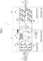
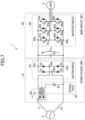
- FIG. 1 shows a power converter (1) which is an electric circuit according to a first embodiment of the present disclosure.
- the power converter (1) converts an alternating current inputted from a power source (2) into an alternating current having desired frequency and voltage and supplies the alternating current to a load (3).
- the power source (2) is a three-phase AC power source.
- the load (3) is a motor.
- the power converter (1) includes a power source unit (10), a main circuit unit (50) configured to receive electric power from the power source (2) via the power source unit (10), and a control device (not shown).
- the power source unit (10) includes a rectifier circuit (20), a main winding (30), and a bypass path (40).
- the rectifier circuit (20) rectifies a three-phase alternating current outputted from the power source (2) to first to third power lines (L1 to L3) into a direct current.
- the rectifier circuit (20) includes first to third input terminals (20a to 20c) connected to the first to third power lines (L1 to L3), and first and second output terminals (20d, 20e) for outputting a direct current.
- the rectifier circuit (20) is a full-wave rectifier circuit.
- the rectifier circuit (20) includes six diodes (21 to 26) that serve as bridge-connected rectifier elements. The diodes (21 to 26) have cathodes directed toward the first output terminal (20d) and anodes directed toward the second output terminal (20e).
- the main winding (30) is provided on a path for supplying the electric power from the power source (2) to the main circuit unit (50). Specifically, one end of the main winding (30) is connected to the first output terminal (20d) of the rectifier circuit (20), and the other end of the main winding (30) is connected to the main circuit unit (50) which will be described later in detail. That is, the main winding (30) is connected in series to the rectifier circuit (20) and the main circuit unit (50).
- Both ends of the bypass path (40) are connected to the first and second output terminals (20d, 20e) of the rectifier circuit (20).
- an auxiliary winding (41) magnetically coupled to the main winding (30) and a varistor (42) that serves as a surge absorber connected in series to the auxiliary winding (41) are provided in order from the first output terminal (20d).
- the main winding (30) and the auxiliary winding (41) have polarities in the same direction.
- the main winding (30) and the auxiliary winding (41) constitute an impedance increasing circuit (11) configured to increase an equivalent impedance between the power source (2) and the main circuit unit (50) based on the current flowing through the bypass path (40).
- the equivalent impedance means
- the main circuit unit (50) includes an inverter circuit (60) and a capacitor (70).
- the inverter circuit (60) converts the direct current outputted from the rectifier circuit (20) into a three-phase alternating current by a switching operation and supplies the three-phase alternating current to the load (3).
- the inverter circuit (60) is controlled by a control device (not shown) by a pulse width modulation (PWM) method.
- PWM pulse width modulation
- the inverter circuit (60) includes six switching elements (61a to 66a) and six freewheeling diodes (61b to 66b).
- the six switching elements (61a to 66a) are bridge-connected. More specifically, the inverter circuit (60) includes three switching legs connected between first and second input nodes (60a, 60b). Each switching leg is formed by connecting two of the switching elements (61a to 66a) in series.
- the first input node (60a) is connected to the other end of the main winding (30), and the second input node (60b) is connected to the second output terminal (20e) of the rectifier circuit (20).
- a midpoint between the switching element (61a to 63a) of the upper arm and the switching element (64a to 66a) of the lower arm is connected to a coil of each phase (a u-phase coil, a v-phase coil, or a w-phase coil) of the load (3).
- Each of the switching elements (61a to 66a) is connected to a corresponding one of the freewheeling diodes (61b to 66b) in inverse parallel.
- Each of the switching elements (61a to 66a) is constituted of an insulated gate bipolar transistor (IGBT).
- the switching elements (61a to 66a) may be constituted of power metal oxide semiconductor field effect transistors (MOSFETs) including wide bandgap semiconductors such as silicon carbide (SiC) and gallium nitride (GaN).
- the capacitor (70) is connected between the first and second input nodes (60a, 60b) of the inverter circuit (60).
- the capacitor (70) is a film capacitor or a ceramic capacitor.
- the film capacitor and the ceramic capacitor generally have a smaller capacitance than electrolytic capacitors, and thus the capacitor (70) does not sufficiently smooth the output voltage of the rectifier circuit (20). In other words, the capacitor (70) allows the output voltage of the rectifier circuit (20) to pulsate.
- the voltage between the first and second input nodes (60a, 60b) of the inverter circuit (60) has a pulsating component.
- the rectifier circuit (20) performs full-wave rectification, and thus the frequency of the pulsating component is 2N times the frequency of the AC voltage outputted from the power source (2) (N is the number of phases of the power source (2)).
- the inductance of the main winding (30) and the capacitance of the capacitor (70) are set to meet the following expression 1, where L (H) is the inductance of the main winding (30), fc (Hz) is the carrier frequency of the PWM control of the inverter circuit (60), C (F) is the capacitance of the capacitor (70), and the value of a constant K is 1/4.
- L (H) is the inductance of the main winding (30)
- fc (Hz) the carrier frequency of the PWM control of the inverter circuit (60)
- C (F) is the capacitance of the capacitor (70)
- the value of a constant K is 1/4.
- the switching elements (61a to 66a) may be power MOSFETs which are made of silicon carbide or gallium nitride and can perform high speed switching. This can increase the carrier frequency fc, and can reduce the inductance of the main winding (30) and the capacitance of the capacitor (70).
- the capacitance of the capacitor (70) is set to meet the following expression 2, where Vac (V) is the voltage of the power source (2) and Pmax (W) is the maximum power consumption of the load (3). [Math 2] C ⁇ 350 ⁇ 10 ⁇ 6 ⁇ Pmax Vac 2
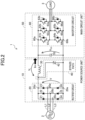
- FIG. 2 shows a power converter (1) of a comparative example.
- the bypass path (40) of the power converter (1) has no auxiliary winding (41).
- the other configuration of the comparative example is the same as, or similar to, that of the first embodiment.
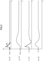
- FIG. 3 shows the voltage Vb across the bypass path (40), the input voltage VDC of the main circuit unit (50), the voltage VL in the main winding (30), and the current Im in the main winding (30) measured in the comparative example in order from the top.
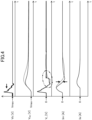
- FIG. 4 shows the voltage Vb across the bypass path (40), the input voltage VDC of the main circuit unit (50), the voltage VL in the main winding (30), the current Im in the main winding (30), and the current Is in the auxiliary winding (41) measured in the first embodiment in order from the top with solid lines.
- Vb across the bypass path (40), the input voltage VDC of the main circuit unit (50), the voltage VL in the main winding (30), and the current Im in the main winding (30) measured in the comparative example with broken lines.
- the voltages and currents shown in FIGS. 3 and 4 are those obtained when the switching of the switching elements (61a to 66a) of the inverter circuit (60) is stopped by the control of the control device (not shown).
- Vmax represents a peak value of the power source voltage supplied by the power source (2) when no lightning surge occurs.
- the voltage Vb across the bypass path (40) increases as indicated by an arrow in FIG. 4 .
- the current Im including the lightning surge current flows through the main winding (30), and electric charges gradually build up in the capacitor (70), increasing the input voltage VDC of the main circuit unit (50).
- the lightning surge current is a current superimposed on a current that flows at a voltage normally supplied from the power source (2). The lightning surge current flows when the voltage of the power source (2) increases in the event of the lightning surge.
- part of the current including the lightning surge current superimposed on the current from the power source (2) flows as the current Is through the bypass path (40) including the auxiliary winding (41), reducing the current flowing from the power source (2) and the power source unit (10) to the main circuit unit (50).
- the auxiliary winding (41) changes the magnetic flux passing through the main winding (30) using the electrical energy sent to the bypass path (40), and generates a voltage in the main winding (30), that is, between the power source (2) and the main circuit unit (50), in a direction that keeps the current including the lightning surge current from flowing through the main circuit unit (50). This increases an equivalent impedance between the power source (2) and the main circuit unit (50).
- the voltage VL in the main winding (30) is higher in the first embodiment than that in the comparative example as can be seen in the part enclosed by the two dot chain line in FIG. 4 .
- the current Im in the main winding (30) is smaller than that in the comparative example.
- the increase of the input voltage VDC of the main circuit unit (50) can be reduced as compared with the comparative example.
- the main circuit unit (50) is less susceptible to damage caused by the lightning surge than in the comparative example.
- the current flowing from the power source (2) to the main winding (30) and the capacitor (70) can be reduced as compared with the comparative example.
- the main winding (30) and the capacitor (70) can be reduced in size as compared with the comparative example.
- the entry of the lightning surge current into the main circuit unit (50) can be blocked by using the electrical energy of the lightning surge current.
- the energy can be effectively used.
- the varistor (42) is provided in the bypass path (40) of the first embodiment, regulating the current flowing through the bypass path (40) when no lightning surge occurs.
- the surge absorber (42) is short-circuited to allow the current to flow through the bypass path (40).
- FIGS. 3 and 4 show the voltages and the currents while the switching of the switching elements (61a to 66a) is stopped. While the switching of the switching elements (61a to 66a) is stopped, the charges in the capacitor (70) do not flow to the load (3), increasing the input voltage VDC of the main circuit unit (50) more significantly. However, the current flowing from the power source (2) to the main winding (30) and the capacitor (70) in the event of the lightning surge can be effectively reduced also when the switching elements (61a to 66a) are caused to perform the switching operation to supply the current to the load (3).
- FIG. 5 shows a power converter (1) according to a variation of the first embodiment of the present disclosure.
- one end of the main winding (30) is connected to the second output terminal (20e) of the rectifier circuit (20), and the other end of the main winding (30) is connected to the second input node (60b) of the inverter circuit (60).
- the first input node (60a) of the inverter circuit (60) is connected to the first output terminal (20d) of the rectifier circuit (20).
- the bypass path (40) is provided with an auxiliary winding (41) and a varistor (42) arranged in order from the second output terminal (20e).
- FIG. 6 shows a power converter (1) according to a second embodiment of the present disclosure.
- first to third main windings (30a to 30c) and first to third bypass paths (40a to 40c) are provided between the power source (2) and the rectifier circuit (20).
- the first main winding (30a) is provided between the power source (2) and the first input terminal (20a) of the rectifier circuit (20), that is, on the first power line (L1).
- the second main winding (30b) is provided between the power source (2) and the second input terminal (20a) of the rectifier circuit (20), that is, on the second power line (L2).
- the third main winding (30c) is provided between the power source (2) and the third input terminal (20c) of the rectifier circuit (20), that is, on the third power line (L3).
- the bypass path (40) includes the first to third bypass paths (40a to 40c).
- One end of the first bypass path (40a) is connected to the first power line (L1) at a position closer to the power source (2) than the first main winding (30a).
- the other end of the first bypass path (40a) is connected to the second power line (L2) at a position closer to the rectifier circuit (20) than the second main winding (30b).
- the auxiliary winding (41) and varistor (42) of the first bypass path (40a) are connected in order from the first power line (L1).
- One end of the second bypass path (40b) is connected to the second power line (L2) at a position closer to the power source (2) than the second main winding (30b).
- the other end of the second bypass path (40b) is connected to the third power line (L3) at a position closer to the rectifier circuit (20) than the third main winding (30c).
- the auxiliary winding (41) and varistor (42) of the second bypass path (40b) are connected in order from the second power line (L2).
- One end of the third bypass path (40c) is connected to the third power line (L3) at a position closer to the power source (2) than the third main winding (30c).
- the other end of the third bypass path (40c) is connected to the first power line (L1) at a position closer to the rectifier circuit (20) than the first main winding (30a).
- the auxiliary winding (41) and varistor (42) of the third bypass path (40c) are connected in order from the third power line (L3).
- the second embodiment is configured in the same manner as the first embodiment except for these features.
- the same components will be indicated by the same reference characters and will not be described in detail.
- FIG. 7 shows a power converter (1) according to a third embodiment of the present disclosure.
- the power source (2) is a single-phase AC power source.
- the rectifier circuit (20) includes only the first and second input terminals (20a, 20b) as the input terminals connected to the first and second power lines (L1, L2).
- the rectifier circuit (20) has four diodes (21 to 24).
- the main winding (30) is provided between the power source (2) and the rectifier circuit (20). That is, the rectifier circuit (20) is connected to the power source (2) via the main winding (30).
- the main winding (30) is provided on the first power line (L1), that is, between the power source (2) and the first input terminal (20a) of the rectifier circuit (20).
- bypass path (40) One end of the bypass path (40) is connected to the first power line (L1) at a position closer to the power source (2) than the main winding (30).
- the other end of the bypass path (40) is connected to the second power line (L2).
- the auxiliary winding (41) and the varistor (42) are connected in order from the first power line (L1).
- the capacitance of the capacitor (70) is set to allow the output voltage of the rectifier circuit (20) to pulsate with the maximum value twice or more the minimum value.
- the third embodiment is configured in the same manner as the first embodiment except for these features.
- the same components will be indicated by the same reference characters and will not be described in detail.
- FIG. 8 shows a power converter (1) according to a variation of the third embodiment of the present disclosure.
- the main winding (30) is provided on the second power line (L2), that is, between the power source (2) and the second input terminal (20b) of the rectifier circuit (20).
- One end of the bypass path (40) is connected to the second power line (L2) at a position closer to the power source (2) than the main winding (30).
- the other end of the bypass path (40) is connected to the first power line (L1).
- the auxiliary winding (41) and the varistor (42) are connected in order from the second power line (L2).
- FIG. 9 shows a power converter (1) according to a fourth embodiment of the present disclosure.
- the power source (2) of the fourth embodiment is a DC power source.
- the power source unit (10) has no rectifier circuit (20).
- the fourth embodiment is configured in the same manner as the first embodiment except for these features. Thus, the same components will be indicated by the same reference characters and will not be described in detail.
- the first embodiment may be modified by using a single-phase AC power source as the power source (2) and replacing the rectifier circuit (20) with the rectifier circuit (20) of the third embodiment, i.e., the rectifier circuit (20) including the four diodes (21 to 24).
- the inverter circuit (60) may be replaced with a different power conversion circuit such as a DC-DC converter capable of performing power conversion such as boosting or stepping down a DC voltage by a switching operation.
- the power conversion circuit may constitute the main circuit unit (50).
- the main circuit unit (50) has the power conversion function by the inverter circuit (60), but the main circuit unit (50) may have no power conversion function.
- the diodes (21 to 26) may be replaced with IGBTs or power MOSFETs including wide bandgap semiconductors such as silicon carbide or gallium nitride in part or all of the rectifier circuit (20).
- the present disclosure is useful as an electric circuit including a power source unit and a main circuit unit configured to receive electric power from a power source via the power source unit.
Landscapes
- Engineering & Computer Science (AREA)
- Power Engineering (AREA)
- Rectifiers (AREA)
- Inverter Devices (AREA)
- Protection Of Static Devices (AREA)
- Control Of Ac Motors In General (AREA)
- Emergency Protection Circuit Devices (AREA)
Abstract
Description
- The present disclosure relates to an electric circuit including a power source unit and a main circuit unit configured to receive electric power from a power source via the power source unit.
-
Patent Document 1 discloses an electric circuit including a power source unit and a main circuit unit configured to receive electric power from an AC power source via the power source unit. In this electric circuit, the power source unit includes a reactor and a converter circuit, and the main circuit unit includes a capacitor and an inverter circuit. - Patent Document 1:
Japanese Unexamined Patent Publication No. 2020-124104 - If lightning strikes, a lightning surge may occur and damage the main circuit unit in the electric circuit disclosed by
Patent Document 1. - In view of this issue, the present disclosure has been made to make the main circuit unit configured to receive the electric power from the power source less susceptible to damage caused by the lightning surge.
- A first aspect is an electric circuit including a power source unit (10) and a main circuit unit (50) configured to receive electric power from a power source (2) via the power source unit (10). The power source unit (10) includes: a bypass path (40, 40a to 40c) configured to allow part of a current including a lightning surge current superimposed on a current from the power source (2) to flow; and an impedance increasing circuit (11) configured to increase an equivalent impedance between the power source (2) and the main circuit unit (50) based on the current flowing through the bypass path (40, 40a to 40c).
- The lightning surge current is a current superimposed on a current that flows at a voltage normally supplied from the power source (2). The lightning surge current flows when a voltage of the power source (2) increases in the event of a lightning surge. In the first aspect, when the lightning surge current is superimposed on the current from the power source (2), part of the current including the lightning surge current is allowed to pass through the bypass path (40, 40a to 40c), and the equivalent impedance between the power source (2) and the main circuit unit (50) is increased. This reduces the current flowing from the power source (2) to the main circuit unit (50). Thus, the main circuit unit (50) is less susceptible to damage caused by the lightning surge.
- A second aspect is an embodiment of the first aspect. In the second aspect, the impedance increasing circuit (11) is configured to increase the impedance using electrical energy sent to the bypass path (40, 40a to 40c) when part of the current including the lightning surge current flows through the bypass path (40, 40a to 40c).
- In the second aspect, the entry of the lightning surge current to the main circuit unit (50) can be blocked by using the electrical energy of the lightning surge current, and thus the energy can be effectively used.
- A third aspect is an embodiment of the first or second aspect. In the third aspect, the impedance increasing circuit (11) is configured to generate a voltage between the power source (2) and the main circuit unit (50) in a direction that keeps the current including the lightning surge current from flowing through the main circuit unit (50) based on the current flowing through the bypass path (40, 40a to 40c).
- A fourth aspect is an embodiment of any one of the first to third aspects. In the fourth aspect, the impedance increasing circuit (11) includes: a main winding (30) provided on a path for supplying the electric power from the power source (2) to the main circuit unit (50); and an auxiliary winding (41) provided on the bypass path (40) and magnetically coupled to the main winding (30), and is configured to generate the voltage by changing a magnetic flux passing through the main winding (30) by passing part of the current including the lightning surge current through the auxiliary winding (41).
- In the fourth aspect, if the lightning surge current is applied between any two lines from the power source (2), the equivalent impedance between the power source (2) and the main circuit unit (50) can be increased to reduce the voltage increase of the main circuit unit (50).
- A fifth aspect is an embodiment of the fourth aspect. In the fifth aspect, the bypass path (40, 40a to 40c) is provided with a surge absorber (42) connected in series to the auxiliary winding (41).
- In the fifth aspect, the surge absorber (42) regulates the flow of the current through the bypass path (40, 40a to 40c) when no lightning surge occurs. On the other hand, when the lightning surge occurs, the surge absorber (42) is short-circuited, and the current flows through the bypass path (40, 40a to 40c). Thus, there is no need to cause a computer to control whether or not to pass the current through the bypass path (40, 40a to 40c), and a delay time from the occurrence of the lightning surge to the flow of the current through the bypass path (40, 40a to 40c) can be shortened.
- A sixth aspect is an embodiment of the fourth or fifth aspect. In the sixth aspect, the main winding (30) and the auxiliary winding (41) have polarities in the same direction.
- In the sixth aspect, when the current flows through the bypass path (40, 40a to 40c), the main winding (30) can generate a voltage in a direction that keeps the current including the lightning surge current from flowing through the main circuit unit (50).
- A seventh aspect is an embodiment of any one of the first to sixth aspects. In the seventh aspect, the power source (2) is an AC power source, the power source unit (10) includes a rectifier circuit (20) configured to rectify an alternating current outputted from the power source (2), and the main circuit unit (50) includes an inverter circuit (60) configured to convert a direct current outputted from the rectifier circuit (20) to an alternating current by a switching operation and a capacitor (70) connected between input nodes (60a, 60b) of the inverter circuit (60) and configured to allow an output voltage of the rectifier circuit (20) to pulsate.
- In the seventh aspect, when the lightning surge current is superimposed on the current from the power source (2), the current flowing from the power source (2) to the capacitor (70) can be reduced to reduce a voltage increase of the capacitor (70). Thus, the capacitor (70) can be reduced in size.
-
-
FIG. 1 is a circuit diagram showing a configuration of a power converter as an electric circuit according to a first embodiment of the present disclosure. -
FIG. 2 is a view corresponding toFIG. 1 , illustrating a comparative example. -
FIG. 3 is a chart showing a voltage across a bypass path, an input voltage of a main circuit unit, a voltage in a main winding, and an input current of the main circuit unit measured in the comparative example. -
FIG. 4 is a timing chart showing a voltage across a bypass path, an input voltage of a main circuit unit, a voltage in a main winding, an input current of the main circuit unit, and a voltage in an auxiliary winding measured in the first embodiment with solid lines, and the voltage across the bypass path, the input voltage of the main circuit unit, the voltage in the main winding, and the input current of the main circuit unit measured in the comparative example with broken lines. -
FIG. 5 is a view corresponding toFIG. 1 , illustrating a variation of the first embodiment. -
FIG. 6 is a view corresponding toFIG. 1 , illustrating a second embodiment. -
FIG. 7 is a view corresponding toFIG. 1 , illustrating a third embodiment. -
FIG. 8 is a view corresponding toFIG. 1 , illustrating a variation of the third embodiment. -
FIG. 9 is a view corresponding toFIG. 1 , illustrating a fourth embodiment. - Embodiments of the present disclosure will be described in detail with reference to the drawings. The following embodiments are merely exemplary ones in nature, and are not intended to limit the scope, application, or use of the present invention.
-
FIG. 1 shows a power converter (1) which is an electric circuit according to a first embodiment of the present disclosure. The power converter (1) converts an alternating current inputted from a power source (2) into an alternating current having desired frequency and voltage and supplies the alternating current to a load (3). The power source (2) is a three-phase AC power source. The load (3) is a motor. - The power converter (1) includes a power source unit (10), a main circuit unit (50) configured to receive electric power from the power source (2) via the power source unit (10), and a control device (not shown).
- The power source unit (10) includes a rectifier circuit (20), a main winding (30), and a bypass path (40).
- The rectifier circuit (20) rectifies a three-phase alternating current outputted from the power source (2) to first to third power lines (L1 to L3) into a direct current. The rectifier circuit (20) includes first to third input terminals (20a to 20c) connected to the first to third power lines (L1 to L3), and first and second output terminals (20d, 20e) for outputting a direct current. Specifically, the rectifier circuit (20) is a full-wave rectifier circuit. The rectifier circuit (20) includes six diodes (21 to 26) that serve as bridge-connected rectifier elements. The diodes (21 to 26) have cathodes directed toward the first output terminal (20d) and anodes directed toward the second output terminal (20e).
- The main winding (30) is provided on a path for supplying the electric power from the power source (2) to the main circuit unit (50). Specifically, one end of the main winding (30) is connected to the first output terminal (20d) of the rectifier circuit (20), and the other end of the main winding (30) is connected to the main circuit unit (50) which will be described later in detail. That is, the main winding (30) is connected in series to the rectifier circuit (20) and the main circuit unit (50).
- Both ends of the bypass path (40) are connected to the first and second output terminals (20d, 20e) of the rectifier circuit (20). In the bypass path (40), an auxiliary winding (41) magnetically coupled to the main winding (30) and a varistor (42) that serves as a surge absorber connected in series to the auxiliary winding (41) are provided in order from the first output terminal (20d). The main winding (30) and the auxiliary winding (41) have polarities in the same direction.
- The main winding (30) and the auxiliary winding (41) constitute an impedance increasing circuit (11) configured to increase an equivalent impedance between the power source (2) and the main circuit unit (50) based on the current flowing through the bypass path (40). The equivalent impedance means |Vb|/|Im|, where Vb is a voltage across the bypass path (40) and Im is a current flowing from the power source unit (10) to the main circuit unit (50).
- The main circuit unit (50) includes an inverter circuit (60) and a capacitor (70).
- The inverter circuit (60) converts the direct current outputted from the rectifier circuit (20) into a three-phase alternating current by a switching operation and supplies the three-phase alternating current to the load (3). The inverter circuit (60) is controlled by a control device (not shown) by a pulse width modulation (PWM) method. Specifically, the inverter circuit (60) includes six switching elements (61a to 66a) and six freewheeling diodes (61b to 66b). The six switching elements (61a to 66a) are bridge-connected. More specifically, the inverter circuit (60) includes three switching legs connected between first and second input nodes (60a, 60b). Each switching leg is formed by connecting two of the switching elements (61a to 66a) in series. The first input node (60a) is connected to the other end of the main winding (30), and the second input node (60b) is connected to the second output terminal (20e) of the rectifier circuit (20).
- In each of the three switching legs, a midpoint between the switching element (61a to 63a) of the upper arm and the switching element (64a to 66a) of the lower arm is connected to a coil of each phase (a u-phase coil, a v-phase coil, or a w-phase coil) of the load (3). Each of the switching elements (61a to 66a) is connected to a corresponding one of the freewheeling diodes (61b to 66b) in inverse parallel. Each of the switching elements (61a to 66a) is constituted of an insulated gate bipolar transistor (IGBT). However, the switching elements (61a to 66a) may be constituted of power metal oxide semiconductor field effect transistors (MOSFETs) including wide bandgap semiconductors such as silicon carbide (SiC) and gallium nitride (GaN).
- The capacitor (70) is connected between the first and second input nodes (60a, 60b) of the inverter circuit (60). The capacitor (70) is a film capacitor or a ceramic capacitor. The film capacitor and the ceramic capacitor generally have a smaller capacitance than electrolytic capacitors, and thus the capacitor (70) does not sufficiently smooth the output voltage of the rectifier circuit (20). In other words, the capacitor (70) allows the output voltage of the rectifier circuit (20) to pulsate. Thus, the voltage between the first and second input nodes (60a, 60b) of the inverter circuit (60) has a pulsating component. The rectifier circuit (20) performs full-wave rectification, and thus the frequency of the pulsating component is 2N times the frequency of the AC voltage outputted from the power source (2) (N is the number of phases of the power source (2)).
- Here, the inductance of the main winding (30) and the capacitance of the capacitor (70) are set to meet the following
expression 1, where L (H) is the inductance of the main winding (30), fc (Hz) is the carrier frequency of the PWM control of the inverter circuit (60), C (F) is the capacitance of the capacitor (70), and the value of a constant K is 1/4.
[Math 1]
- This allows the main winding (30) and the capacitor (70) to absorb switching noise generated in the inverter circuit (60). The switching elements (61a to 66a) may be power MOSFETs which are made of silicon carbide or gallium nitride and can perform high speed switching. This can increase the carrier frequency fc, and can reduce the inductance of the main winding (30) and the capacitance of the capacitor (70).
- The capacitance of the capacitor (70) is set to meet the following
expression 2, where Vac (V) is the voltage of the power source (2) and Pmax (W) is the maximum power consumption of the load (3).
[Math 2]
- Setting the capacitance of the capacitor (70) in this manner can reduce the fifth and seventh harmonics from the rectifier circuit (20).
-
FIG. 2 shows a power converter (1) of a comparative example. In this comparative example, the bypass path (40) of the power converter (1) has no auxiliary winding (41). The other configuration of the comparative example is the same as, or similar to, that of the first embodiment. -
FIG. 3 shows the voltage Vb across the bypass path (40), the input voltage VDC of the main circuit unit (50), the voltage VL in the main winding (30), and the current Im in the main winding (30) measured in the comparative example in order from the top.FIG. 4 shows the voltage Vb across the bypass path (40), the input voltage VDC of the main circuit unit (50), the voltage VL in the main winding (30), the current Im in the main winding (30), and the current Is in the auxiliary winding (41) measured in the first embodiment in order from the top with solid lines.FIG. 4 also shows the voltage Vb across the bypass path (40), the input voltage VDC of the main circuit unit (50), the voltage VL in the main winding (30), and the current Im in the main winding (30) measured in the comparative example with broken lines. The voltages and currents shown inFIGS. 3 and4 are those obtained when the switching of the switching elements (61a to 66a) of the inverter circuit (60) is stopped by the control of the control device (not shown). InFIGS. 3 and4 , Vmax represents a peak value of the power source voltage supplied by the power source (2) when no lightning surge occurs. - If the lightning surge occurs in the circuit of the first embodiment, the voltage Vb across the bypass path (40) increases as indicated by an arrow in
FIG. 4 . In response to the voltage increase, the current Im including the lightning surge current flows through the main winding (30), and electric charges gradually build up in the capacitor (70), increasing the input voltage VDC of the main circuit unit (50). The lightning surge current is a current superimposed on a current that flows at a voltage normally supplied from the power source (2). The lightning surge current flows when the voltage of the power source (2) increases in the event of the lightning surge. Further, part of the current including the lightning surge current superimposed on the current from the power source (2) flows as the current Is through the bypass path (40) including the auxiliary winding (41), reducing the current flowing from the power source (2) and the power source unit (10) to the main circuit unit (50). When the current Is flows through the bypass path (40), the auxiliary winding (41) changes the magnetic flux passing through the main winding (30) using the electrical energy sent to the bypass path (40), and generates a voltage in the main winding (30), that is, between the power source (2) and the main circuit unit (50), in a direction that keeps the current including the lightning surge current from flowing through the main circuit unit (50). This increases an equivalent impedance between the power source (2) and the main circuit unit (50). Thus, when the current Is flows through the bypass path (40) in the event of the lightning surge, the voltage VL in the main winding (30) is higher in the first embodiment than that in the comparative example as can be seen in the part enclosed by the two dot chain line inFIG. 4 . As indicated by the arrow inFIG. 4 , the current Im in the main winding (30) is smaller than that in the comparative example. As a result, the increase of the input voltage VDC of the main circuit unit (50) can be reduced as compared with the comparative example. Thus, the main circuit unit (50) is less susceptible to damage caused by the lightning surge than in the comparative example. - In the first embodiment, when the lightning surge current is superimposed on the current from the power source (2), the current flowing from the power source (2) to the main winding (30) and the capacitor (70) can be reduced as compared with the comparative example. Thus, the main winding (30) and the capacitor (70) can be reduced in size as compared with the comparative example.
- In the first embodiment, the entry of the lightning surge current into the main circuit unit (50) can be blocked by using the electrical energy of the lightning surge current. Thus, the energy can be effectively used.
- Further, the varistor (42) is provided in the bypass path (40) of the first embodiment, regulating the current flowing through the bypass path (40) when no lightning surge occurs. In the event of the lightning surge, the surge absorber (42) is short-circuited to allow the current to flow through the bypass path (40). Thus, there is no need to cause a computer to control whether or not to pass the current through the bypass path (40), and a delay time from the occurrence of the lightning surge to the flow of the current through the bypass path (40) can be shortened.
-
FIGS. 3 and4 show the voltages and the currents while the switching of the switching elements (61a to 66a) is stopped. While the switching of the switching elements (61a to 66a) is stopped, the charges in the capacitor (70) do not flow to the load (3), increasing the input voltage VDC of the main circuit unit (50) more significantly. However, the current flowing from the power source (2) to the main winding (30) and the capacitor (70) in the event of the lightning surge can be effectively reduced also when the switching elements (61a to 66a) are caused to perform the switching operation to supply the current to the load (3). -
FIG. 5 shows a power converter (1) according to a variation of the first embodiment of the present disclosure. In this variation, one end of the main winding (30) is connected to the second output terminal (20e) of the rectifier circuit (20), and the other end of the main winding (30) is connected to the second input node (60b) of the inverter circuit (60). The first input node (60a) of the inverter circuit (60) is connected to the first output terminal (20d) of the rectifier circuit (20). The bypass path (40) is provided with an auxiliary winding (41) and a varistor (42) arranged in order from the second output terminal (20e). - This variation is configured in the same manner as the first embodiment except for these features. Thus, the same components will be indicated by the same reference characters and will not be described in detail.
-
FIG. 6 shows a power converter (1) according to a second embodiment of the present disclosure. According to the second embodiment, first to third main windings (30a to 30c) and first to third bypass paths (40a to 40c) are provided between the power source (2) and the rectifier circuit (20). - Specifically, the first main winding (30a) is provided between the power source (2) and the first input terminal (20a) of the rectifier circuit (20), that is, on the first power line (L1).
- The second main winding (30b) is provided between the power source (2) and the second input terminal (20a) of the rectifier circuit (20), that is, on the second power line (L2).
- The third main winding (30c) is provided between the power source (2) and the third input terminal (20c) of the rectifier circuit (20), that is, on the third power line (L3).
- The bypass path (40) includes the first to third bypass paths (40a to 40c).
- One end of the first bypass path (40a) is connected to the first power line (L1) at a position closer to the power source (2) than the first main winding (30a). The other end of the first bypass path (40a) is connected to the second power line (L2) at a position closer to the rectifier circuit (20) than the second main winding (30b). The auxiliary winding (41) and varistor (42) of the first bypass path (40a) are connected in order from the first power line (L1).
- One end of the second bypass path (40b) is connected to the second power line (L2) at a position closer to the power source (2) than the second main winding (30b). The other end of the second bypass path (40b) is connected to the third power line (L3) at a position closer to the rectifier circuit (20) than the third main winding (30c). The auxiliary winding (41) and varistor (42) of the second bypass path (40b) are connected in order from the second power line (L2).
- One end of the third bypass path (40c) is connected to the third power line (L3) at a position closer to the power source (2) than the third main winding (30c). The other end of the third bypass path (40c) is connected to the first power line (L1) at a position closer to the rectifier circuit (20) than the first main winding (30a). The auxiliary winding (41) and varistor (42) of the third bypass path (40c) are connected in order from the third power line (L3).
- The second embodiment is configured in the same manner as the first embodiment except for these features. Thus, the same components will be indicated by the same reference characters and will not be described in detail.
-
FIG. 7 shows a power converter (1) according to a third embodiment of the present disclosure. In the third embodiment, the power source (2) is a single-phase AC power source. Thus, the rectifier circuit (20) includes only the first and second input terminals (20a, 20b) as the input terminals connected to the first and second power lines (L1, L2). The rectifier circuit (20) has four diodes (21 to 24). The main winding (30) is provided between the power source (2) and the rectifier circuit (20). That is, the rectifier circuit (20) is connected to the power source (2) via the main winding (30). - Specifically, the main winding (30) is provided on the first power line (L1), that is, between the power source (2) and the first input terminal (20a) of the rectifier circuit (20).
- One end of the bypass path (40) is connected to the first power line (L1) at a position closer to the power source (2) than the main winding (30). The other end of the bypass path (40) is connected to the second power line (L2). The auxiliary winding (41) and the varistor (42) are connected in order from the first power line (L1).
- The capacitance of the capacitor (70) is set to allow the output voltage of the rectifier circuit (20) to pulsate with the maximum value twice or more the minimum value.
- The third embodiment is configured in the same manner as the first embodiment except for these features. Thus, the same components will be indicated by the same reference characters and will not be described in detail.
-
FIG. 8 shows a power converter (1) according to a variation of the third embodiment of the present disclosure. In this variation, the main winding (30) is provided on the second power line (L2), that is, between the power source (2) and the second input terminal (20b) of the rectifier circuit (20). One end of the bypass path (40) is connected to the second power line (L2) at a position closer to the power source (2) than the main winding (30). The other end of the bypass path (40) is connected to the first power line (L1). The auxiliary winding (41) and the varistor (42) are connected in order from the second power line (L2). - This variation is configured in the same manner as the third embodiment except for these features. Thus, the same components will be indicated by the same reference characters and will not be described in detail.
-
FIG. 9 shows a power converter (1) according to a fourth embodiment of the present disclosure. The power source (2) of the fourth embodiment is a DC power source. The power source unit (10) has no rectifier circuit (20). - The fourth embodiment is configured in the same manner as the first embodiment except for these features. Thus, the same components will be indicated by the same reference characters and will not be described in detail.
- The first embodiment may be modified by using a single-phase AC power source as the power source (2) and replacing the rectifier circuit (20) with the rectifier circuit (20) of the third embodiment, i.e., the rectifier circuit (20) including the four diodes (21 to 24).
- In the first to fourth embodiments and the variations of the first and third embodiments, the inverter circuit (60) may be replaced with a different power conversion circuit such as a DC-DC converter capable of performing power conversion such as boosting or stepping down a DC voltage by a switching operation. The power conversion circuit may constitute the main circuit unit (50).
- In the first to fourth embodiments and the variations of the first and third embodiments, the main circuit unit (50) has the power conversion function by the inverter circuit (60), but the main circuit unit (50) may have no power conversion function.
- In the first to fourth embodiments and the variations of the first and third embodiments, the diodes (21 to 26) may be replaced with IGBTs or power MOSFETs including wide bandgap semiconductors such as silicon carbide or gallium nitride in part or all of the rectifier circuit (20).
- It will be understood that the embodiments and variations described above can be modified with various changes in form and details without departing from the spirit and scope of the claims. The above embodiments and variations may be appropriately combined or replaced as long as the functions of the target of the present disclosure are not impaired.
- As can be seen in the foregoing, the present disclosure is useful as an electric circuit including a power source unit and a main circuit unit configured to receive electric power from a power source via the power source unit.
-
- 1
- Power Converter
- 2
- Power Source
- 10
- Power Source Unit
- 11
- Impedance Increasing Circuit
- 20
- Rectifier Circuit
- 30
- Main Winding
- 40
- Bypass Path
- 41
- Auxiliary Winding
- 42
- Varistor (Surge Absorber)
- 50
- Main Circuit Unit
- 60
- Inverter Circuit
- 60a
- First Input Node
- 60b
- Second Input Node
- 70
- Capacitor
Claims (7)
- An electric circuit including a power source unit (10) and a main circuit unit (50) configured to receive electric power from a power source (2) via the power source unit (10), wherein
the power source unit (10) includes:a bypass path (40, 40a to 40c) configured to allow part of a current including a lightning surge current superimposed on a current from the power source (2) to flow; andan impedance increasing circuit (11) configured to increase an equivalent impedance between the power source (2) and the main circuit unit (50) based on the current flowing through the bypass path (40, 40a to 40c). - The electric circuit of claim 1, wherein
the impedance increasing circuit (11) is configured to increase the impedance using electrical energy sent to the bypass path (40, 40a to 40c) when part of the current including the lightning surge current flows through the bypass path (40, 40a to 40c). - The electric circuit of claim 1 or 2, wherein
the impedance increasing circuit (11) is configured to generate a voltage between the power source (2) and the main circuit unit (50) in a direction that keeps the current including the lightning surge current from flowing through the main circuit unit (50) based on the current flowing through the bypass path (40, 40a to 40c). - The electric circuit of any one of claims 1 to 3, wherein
the impedance increasing circuit (11) includes: a main winding (30) provided on a path for supplying the electric power from the power source (2) to the main circuit unit (50); and an auxiliary winding (41) provided on the bypass path (40) and magnetically coupled to the main winding (30), and is configured to generate the voltage by changing a magnetic flux passing through the main winding (30) by passing part of the current including the lightning surge current through the auxiliary winding (41). - The electric circuit of claim 4, wherein
the bypass path (40, 40a to 40c) is provided with a surge absorber (42) connected in series to the auxiliary winding (41). - The electric circuit of claim 4 or 5, wherein
the main winding (30) and the auxiliary winding (41) have polarities in the same direction. - The electric circuit of any one of claims 1 to 6, whereinthe power source (2) is an AC power source,the power source unit (10) includes:
a rectifier circuit (20) configured to rectify an alternating current outputted from the power source (2), andthe main circuit unit (50) includesan inverter circuit (60) configured to convert a direct current outputted from the rectifier circuit (20) to an alternating current by a switching operation anda capacitor (70) connected between input nodes (60a, 60b) of the inverter circuit (60) and configured to allow an output voltage of the rectifier circuit (20) to pulsate.
Applications Claiming Priority (2)
| Application Number | Priority Date | Filing Date | Title |
|---|---|---|---|
| JP2022157757A JP7421144B1 (en) | 2022-09-30 | 2022-09-30 | electric circuit |
| PCT/JP2023/031591 WO2024070456A1 (en) | 2022-09-30 | 2023-08-30 | Electric circuit |
Publications (2)
| Publication Number | Publication Date |
|---|---|
| EP4576468A1 true EP4576468A1 (en) | 2025-06-25 |
| EP4576468A4 EP4576468A4 (en) | 2025-12-17 |
Family
ID=89616002
Family Applications (1)
| Application Number | Title | Priority Date | Filing Date |
|---|---|---|---|
| EP23871696.3A Pending EP4576468A4 (en) | 2022-09-30 | 2023-08-30 | ELECTRICAL CIRCUIT |
Country Status (5)
| Country | Link |
|---|---|
| US (1) | US20250226768A1 (en) |
| EP (1) | EP4576468A4 (en) |
| JP (2) | JP7421144B1 (en) |
| CN (1) | CN119856354A (en) |
| WO (1) | WO2024070456A1 (en) |
Family Cites Families (7)
| Publication number | Priority date | Publication date | Assignee | Title |
|---|---|---|---|---|
| JPH0649113Y2 (en) * | 1989-12-27 | 1994-12-12 | いすゞ自動車株式会社 | Vehicle power supply |
| JP3672552B2 (en) * | 2002-12-26 | 2005-07-20 | 株式会社エヌ・ティ・ティ・データ・イー・エックス・テクノ | Overvoltage overcurrent protection circuit |
| JP2004320851A (en) * | 2003-04-14 | 2004-11-11 | Chofu Seisakusho Co Ltd | Power supply |
| JP4752484B2 (en) * | 2005-12-14 | 2011-08-17 | サンケン電気株式会社 | DC-DC converter |
| JP5427356B2 (en) * | 2007-12-14 | 2014-02-26 | 任天堂株式会社 | Overvoltage protection circuit and electronic device including the same |
| JP2015128357A (en) * | 2013-12-27 | 2015-07-09 | ダイキン工業株式会社 | Overvoltage protection circuit and power conversion device including the same |
| CN113366752B (en) | 2019-01-30 | 2024-11-05 | 大金工业株式会社 | Power conversion device |
-
2022
- 2022-09-30 JP JP2022157757A patent/JP7421144B1/en active Active
-
2023
- 2023-08-30 WO PCT/JP2023/031591 patent/WO2024070456A1/en not_active Ceased
- 2023-08-30 CN CN202380064848.8A patent/CN119856354A/en active Pending
- 2023-08-30 EP EP23871696.3A patent/EP4576468A4/en active Pending
-
2024
- 2024-01-09 JP JP2024001352A patent/JP2024052669A/en active Pending
-
2025
- 2025-03-26 US US19/091,547 patent/US20250226768A1/en active Pending
Also Published As
| Publication number | Publication date |
|---|---|
| EP4576468A4 (en) | 2025-12-17 |
| JP7421144B1 (en) | 2024-01-24 |
| US20250226768A1 (en) | 2025-07-10 |
| CN119856354A (en) | 2025-04-18 |
| WO2024070456A1 (en) | 2024-04-04 |
| JP2024052669A (en) | 2024-04-11 |
| JP2024051538A (en) | 2024-04-11 |
Similar Documents
| Publication | Publication Date | Title |
|---|---|---|
| US8861235B2 (en) | Power converting apparatus | |
| Mohr et al. | Converter systems for fuel cells in the medium power range—A comparative study | |
| US10320278B2 (en) | Semiconductor device having a decreased switching loss | |
| CN102570967B (en) | Low inductance, high efficiency induction machine and manufacture method thereof | |
| US11177741B2 (en) | AC-AC converter circuit | |
| US10050560B1 (en) | Inverter circuit with current detection circuitry | |
| CN1309155C (en) | Switching power supply circuit and inverter device | |
| CN119382534A (en) | Power conversion device | |
| US9899917B2 (en) | Method for producing an output voltage and assembly for performing the method | |
| EP3707816B1 (en) | Inverter with ac forward bridge and improved dc/dc topology | |
| EP2509207A2 (en) | Power conversion system | |
| EP3694096A1 (en) | Three-level pulse width modulation technique for reducing semiconductor short circuit conduction loss | |
| Rabi et al. | Harmonics study and comparison of Z-source inverter with traditional inverters | |
| Suresh et al. | Simulation of Z-source inverter using maximum boost control PWM technique | |
| US8064232B2 (en) | Power conversion device and power conversion system | |
| CN109643958B (en) | Power conversion device | |
| US20250226768A1 (en) | Electric circuit | |
| JP3171551B2 (en) | High voltage output power converter | |
| CN111835215A (en) | Converter circuit, power conversion system, and motor drive device | |
| WO2021156981A1 (en) | Switching converter | |
| JP3736997B2 (en) | Pulse width modulation controlled converter | |
| Magne et al. | Fundamentals of power electronics | |
| RU2808147C1 (en) | Single-cycle power factor correction control method | |
| EP4693877A1 (en) | Inverter device, motor drive device including same, and refrigeration device | |
| Gorbunov | Power conversion efficiency of AC buck voltage converter |
Legal Events
| Date | Code | Title | Description |
|---|---|---|---|
| STAA | Information on the status of an ep patent application or granted ep patent |
Free format text: STATUS: THE INTERNATIONAL PUBLICATION HAS BEEN MADE |
|
| PUAI | Public reference made under article 153(3) epc to a published international application that has entered the european phase |
Free format text: ORIGINAL CODE: 0009012 |
|
| STAA | Information on the status of an ep patent application or granted ep patent |
Free format text: STATUS: REQUEST FOR EXAMINATION WAS MADE |
|
| 17P | Request for examination filed |
Effective date: 20250318 |
|
| AK | Designated contracting states |
Kind code of ref document: A1 Designated state(s): AL AT BE BG CH CY CZ DE DK EE ES FI FR GB GR HR HU IE IS IT LI LT LU LV MC ME MK MT NL NO PL PT RO RS SE SI SK SM TR |
|
| P01 | Opt-out of the competence of the unified patent court (upc) registered |
Free format text: CASE NUMBER: UPC_APP_3795_4576468/2025 Effective date: 20250820 |
|
| REG | Reference to a national code |
Ref country code: DE Ref legal event code: R079 Free format text: PREVIOUS MAIN CLASS: H02H0009020000 Ipc: H02H0009040000 |
|
| A4 | Supplementary search report drawn up and despatched |
Effective date: 20251117 |
|
| RIC1 | Information provided on ipc code assigned before grant |
Ipc: H02H 9/04 20060101AFI20251111BHEP Ipc: H02M 7/48 20070101ALI20251111BHEP Ipc: H02H 3/20 20060101ALI20251111BHEP Ipc: H02M 1/32 20070101ALI20251111BHEP Ipc: H02H 9/02 20060101ALN20251111BHEP |
|
| DAV | Request for validation of the european patent (deleted) | ||
| DAX | Request for extension of the european patent (deleted) | ||
| GRAP | Despatch of communication of intention to grant a patent |
Free format text: ORIGINAL CODE: EPIDOSNIGR1 |
|
| STAA | Information on the status of an ep patent application or granted ep patent |
Free format text: STATUS: GRANT OF PATENT IS INTENDED |