EP4576434A1 - Assembly for electrical conduction between a plate and a pin - Google Patents
Assembly for electrical conduction between a plate and a pin Download PDFInfo
- Publication number
- EP4576434A1 EP4576434A1 EP23383345.8A EP23383345A EP4576434A1 EP 4576434 A1 EP4576434 A1 EP 4576434A1 EP 23383345 A EP23383345 A EP 23383345A EP 4576434 A1 EP4576434 A1 EP 4576434A1
- Authority
- EP
- European Patent Office
- Prior art keywords
- pin
- neck
- plate
- hole
- electrically conductive
- Prior art date
- Legal status (The legal status is an assumption and is not a legal conclusion. Google has not performed a legal analysis and makes no representation as to the accuracy of the status listed.)
- Pending
Links
Images

Classifications
-
- H—ELECTRICITY
- H01—ELECTRIC ELEMENTS
- H01R—ELECTRICALLY-CONDUCTIVE CONNECTIONS; STRUCTURAL ASSOCIATIONS OF A PLURALITY OF MUTUALLY-INSULATED ELECTRICAL CONNECTING ELEMENTS; COUPLING DEVICES; CURRENT COLLECTORS
- H01R4/00—Electrically-conductive connections between two or more conductive members in direct contact, i.e. touching one another; Means for effecting or maintaining such contact; Electrically-conductive connections having two or more spaced connecting locations for conductors and using contact members penetrating insulation
- H01R4/02—Soldered or welded connections
- H01R4/029—Welded connections
-
- H—ELECTRICITY
- H01—ELECTRIC ELEMENTS
- H01R—ELECTRICALLY-CONDUCTIVE CONNECTIONS; STRUCTURAL ASSOCIATIONS OF A PLURALITY OF MUTUALLY-INSULATED ELECTRICAL CONNECTING ELEMENTS; COUPLING DEVICES; CURRENT COLLECTORS
- H01R4/00—Electrically-conductive connections between two or more conductive members in direct contact, i.e. touching one another; Means for effecting or maintaining such contact; Electrically-conductive connections having two or more spaced connecting locations for conductors and using contact members penetrating insulation
- H01R4/10—Electrically-conductive connections between two or more conductive members in direct contact, i.e. touching one another; Means for effecting or maintaining such contact; Electrically-conductive connections having two or more spaced connecting locations for conductors and using contact members penetrating insulation effected solely by twisting, wrapping, bending, crimping, or other permanent deformation
Definitions
- the present invention concerns a plate, which is electrically conductive, an assembly configured for electrical conduction between the plate and a pin, which is electrically conductive, and a method for connecting a pin with a plate electrically.
- Electronic devices are used in various applications. Different assemblies were developed to connect electric devices to required power and voltage sources. A common method is to use an electrically conductive busbar.
- terminals of the electrical devices have to be electrically connected to and mechanically fixed to the bus bar.
- the bus bars are relatively thick, high energy input is required to connect terminals and bus bars. Thus, the temperature at the terminal can reach high temperatures exceeding the maximum allowable operating temperatures and thus causing damages at the terminal.
- a task of the present invention is thus to provide a plate and an assembly which allow a reliable electrical connection of the plate and a corresponding assembling method.
- a plate which is electrically conductive.
- the plate comprises a hole surrounded by a neck.
- the hole and the surrounding neck are configured for insertion of an electrically conductive terminal, like, e.g., a pin.
- the pin is an electrical terminal which can have any shape, e.g., a cylindrical shape, a cuboid shape, preferably a rectangular cuboid shape, a needle shape, or a cubic shape.
- the neck provides a comparably large contact area for electrical and mechanical connection and fixation with the pin.
- the shape of the neck does preferably positively fit to the shape of the pin and vice versa.
- the neck has a smaller wall thickness than the plate.
- the small wall thickness allows heating of the neck with low effort and low energy input. This facilitates welding and soldering processes at an edge of the neck. In particular, overheating or damaging of the pin can be avoided when welding or soldering the pin to the neck.
- the neck is formed in one piece with the plate. This allows a simple structure and simple manufacturing. Preferably, the neck is punched out of the plate.
- the plate has preferably a plate thickness of 0.05 to 5 mm, more preferable of 0.1 to 3 mm, or even more preferable 0.2 to 2 mm.
- the plate consists of or comprises a conductive layer with a layer thickness of more than 0.2, or preferably more than 0.5 mm.
- the conductive layer of the plate comprises or consist of a conductive metal or metal alloy, like, e.g., copper.
- the plate does not comprise a support layer other than the conductive layer or layers.
- the plate may also be configured as a strip or a bar.
- the plate consists of one or more electrically conductive metals or metal alloys.
- the whole plate may be electrically conductive.
- the plate may be used as an electrical conductor, particularly, as a busbar.
- a busbar or bus bar is a metallic plate, strip or bar for local high current power distribution.
- the invention further concerns an assembly configured for electrical conduction between the plate according to any embodiments as describe before and a pin, which is electrically conductive.
- the pin can comprise or consist of electrically conductive materials like metals or metal alloys, e.g., copper or aluminum.
- the pin can have a cylindrical shape with a diameter from 0.3 mm to 3 mm, preferably from 0.3 mm to 1.8 mm, more preferably from 0.5 mm to 1.5 mm.
- the assembly comprises the plate and the pin, wherein the pin is inserted into the hole of the plate and is electrically connected to the neck.
- the pin is inserted into the hole and into the neck surrounding the hole.
- the pin is then, preferably, electrically connected to the neck and mechanically fixed to the neck, in particular to an inner surface of the neck.
- the neck structure surrounding the hole facilitates the insertion of the pin into the hole.
- the pin consists of one or more electrically conductive metals or metal alloys.
- the pin is the electrical terminal of an electrical device, which shall be connected to the plate which may be a busbar.
- the pin and the neck are firmly connected by solder or by a welding seam.
- the large contact area provided by the neck guarantees a firm electrical connection and mechanical fixation.
- the electric resistance between the pin and the neck and thus the plate decreases.
- the mechanical resistance, firmness and durability are enhanced.
- the pin and the neck are form-fittingly connected. In this way, the contact area is maximized.
- the assembly comprises several plates.
- the several plates comprise at least one neck each.
- the plates are electrically connected to the pin by the necks.
- Several plates may be connected to one pin or to several pins.
- One electrical plate can be connected to several electrical devices and one electrical device can be connected to several plates.
- the assembly comprises an electrical device which comprises the one or more pins, wherein each pin is electrically connected to one or more of the plates.
- the assembly comprises an insulation sheet that is arranged between two adjacent plates.
- the insulation sheet electrically insulates the plates from each other.
- the insulation device and the plates may be separate components, or the insulation sheet may be configured as an insulation layer of the plate to facilitate the assembly.
- the invention further concerns a method for connecting a pin with a plate, which are both electrically conductive. All components may be configured as described before.
- soldering comprises capillary joining between the pin and the neck. Solder material is sucked in a small gap between the pin and the neck, fulfills the gap and connects the pin and the neck when cured.
- the solder material is pre-deposited on the edge of the neck before inserting the pin in the hole and the surrounding neck. This modification facilitates the handling of the solder material.
- the solder material is not pre-deposited but is added on the edge after insertion of the pin. This allows flexible handling during the manufacturing process.
- the welding is performed as laser welding, which allows very accurate welding.
- other welding processes can be applied like, e.g., Inductive Heating (IH) or tungsten inert gas (TIG) welding.
- IH Inductive Heating
- TOG tungsten inert gas
- Soldering or welding is performed at the neck.
- the neck protrudes out of the plate.
- the wall thickness of the neck is preferably thinner than the thickness of the plate.
- the neck comprises less material than the whole plate.
- Figure 1 shows a first embodiment of the invention. It shows a plate 1 with a punched hole 2 surrounded by a neck 3. The neck 3 and the plate 1 are formed in one piece. Further, figure 1 shows a device 4 provided with a cylindrical pin 5, wherein the pin 5 is inserted into the hole 2 and the surrounding neck 3.
- the diameter of the hole 2 is preferably between 0.5 mm and 3 mm, more preferably between 1 mm and 1.5 mm.
- the neck 3 has preferably a height up to 2.5 mm, preferably between 1.5 mm and 2.5 mm.
- the neck comprises a flat section 3a and a round or chamfered section 3b between the flat section 3a of the neck and the planar section of the plate 1 (see also figure 2 ).
- the height of the chamfered section 3b is preferably between more than 0 mm and 1 mm, more preferably between 0.3 and 0.7 mm.
- the height of the flat section 3a is preferably between 1 mm and 1.5 mm.
- the plate 1 is preferably electrically conductive and comprises or consists of an electrically conductive material, for example an electrically conductive metal or metal alloy, in particular copper (Cu).
- an electrically conductive material for example an electrically conductive metal or metal alloy, in particular copper (Cu).
- the plate 1 may comprise other materials or layers which are not electrically conductive, e.g., a substrate supporting the electrically conductive layer.
- the device 4 is preferably an electrical device like, for example, a capacitor, resistor, transistor, inductor, or any other electrical device 4.
- the device 4 comprises the electrically conductive pin 5 working as an electrical terminal for electrical connection with the plate 1. To connect the plate 1 and the device 4, the pin 5 is inserted into the hole 2 and the surrounding neck 3.
- the neck and the pin positively fit to each other.
- the neck provides a comparably big connection area.
- the surface of the pin 5 snugs on the inner surface of the neck, particularly the connection area of the neck.
- the form-fitting connection between the pin 5 and the neck 3 provides also mechanical stability of the connection.
- solder material 6 may be pre-deposited on an edge 7of the neck.
- the edge 7 shows away from the planar side of the plate.
- a capillary joint 8 is configured between neck 3 and pin 5.
- a typical solder material is a material comprising tin or a tin alloy.
- the solder material has to be heated up to 230 °C to 240 °C for melting.
- the applied heat can be punctually applied to the edge 7 of the neck 3 instead of an edge of the planar plate 1.
- spreading of heat is suppressed and the energy input can be minimized.
- damage of heat sensitive components like the thin pin 5 or of insulation sheets can be avoided.
- the wall thickness of the neck 3 is preferably configured smaller than the wall thickness of the plate 1.
- the joint may be configured by welding with a welding metal like copper.
- the welding temperature has to be higher than the melting temperature of copper, which is 1085 °C.
- the neck allows advantageously lower heat consumption.
- the welding seam 9 at the edge 7 is preferably built by laser welding as this method allows very fine structuring of the seam.
- Figure 5 shows a further embodiment according to the invention which is in principle analogous to the first embodiment.
- the device 4 of the second embodiment comprises two pins 5, each connected to a plate 1.
- the plates 2 are for example metal plates which may work as busbars.
- the metal plates may comprise copper or a copper alloy.
- an insulation sheet 10 is provided, electrically insulating the two plates 2 against each other.
- Figure 6 shows a third embodiment according to the invention which is in principle analogous to the first and the second embodiment.
- the embodiment according to figure 6 shows two main differences. Firstly, the pins 5 are configured rectangular cuboid instead of cylindrical. Secondly, the two plates 2 do not overlap each other.
- the cuboid pins 5 may be elongated in a direction parallel to the plates 2 as shown in figure 6 to maximize the contact area between the pins 5 and the neck 3.
- the shape of the necks 3 is form-fittingly adapted to the shape of the pins 5.
- the length of the necks 3 in the elongated direction may amount around 3 to 15 mm, preferably around 5 to 12 mm, more preferably around 8 to 10 mm.
Landscapes
- Connections Effected By Soldering, Adhesion, Or Permanent Deformation (AREA)
Abstract
The present invention relates to a plate (1), which is electrically conductive, comprising a hole (2) surrounded by a neck (3) configured for insertion of an electrically conductive terminal and an assembly configured for electrical conduction between the plate (1) and a conductive pin (5), wherein the pin (5) is inserted into the hole (2) and electrically connected to the neck (3). The invention also relates to a corresponding manufacturing method.
Description
- The present invention concerns a plate, which is electrically conductive, an assembly configured for electrical conduction between the plate and a pin, which is electrically conductive, and a method for connecting a pin with a plate electrically.
- Electronic devices are used in various applications. Different assemblies were developed to connect electric devices to required power and voltage sources. A common method is to use an electrically conductive busbar.
- In this case, terminals of the electrical devices have to be electrically connected to and mechanically fixed to the bus bar.
- Since the bus bars are relatively thick, high energy input is required to connect terminals and bus bars. Thus, the temperature at the terminal can reach high temperatures exceeding the maximum allowable operating temperatures and thus causing damages at the terminal.
- Further, known types of connections between bus bars and electric devices are often susceptible to faults and unreliable.
- A task of the present invention is thus to provide a plate and an assembly which allow a reliable electrical connection of the plate and a corresponding assembling method.
- The issue may be solved by the embodiments according to the claims.
- In particular, a plate is disclosed, which is electrically conductive. The plate comprises a hole surrounded by a neck. The hole and the surrounding neck are configured for insertion of an electrically conductive terminal, like, e.g., a pin.
- In the understanding of the present text, the term 'pin' shall not limit the shape of the pin. The pin is an electrical terminal which can have any shape, e.g., a cylindrical shape, a cuboid shape, preferably a rectangular cuboid shape, a needle shape, or a cubic shape.
- The neck provides a comparably large contact area for electrical and mechanical connection and fixation with the pin.
- The shape of the neck does preferably positively fit to the shape of the pin and vice versa.
- Further, in an embodiment, the neck has a smaller wall thickness than the plate. The small wall thickness allows heating of the neck with low effort and low energy input. This facilitates welding and soldering processes at an edge of the neck. In particular, overheating or damaging of the pin can be avoided when welding or soldering the pin to the neck.
- In an embodiment of the plate, the neck is formed in one piece with the plate. This allows a simple structure and simple manufacturing. Preferably, the neck is punched out of the plate.
- The plate has preferably a plate thickness of 0.05 to 5 mm, more preferable of 0.1 to 3 mm, or even more preferable 0.2 to 2 mm.
- Preferably, the plate consists of or comprises a conductive layer with a layer thickness of more than 0.2, or preferably more than 0.5 mm.
- The conductive layer of the plate comprises or consist of a conductive metal or metal alloy, like, e.g., copper.
- Preferably, the plate does not comprise a support layer other than the conductive layer or layers.
- In embodiments, the plate may also be configured as a strip or a bar.
- In an embodiment of the plate, the plate consists of one or more electrically conductive metals or metal alloys. For example, the whole plate may be electrically conductive. The plate may be used as an electrical conductor, particularly, as a busbar. In electric power distribution, a busbar or bus bar is a metallic plate, strip or bar for local high current power distribution.
- The invention further concerns an assembly configured for electrical conduction between the plate according to any embodiments as describe before and a pin, which is electrically conductive.
- In particular, the pin can comprise or consist of electrically conductive materials like metals or metal alloys, e.g., copper or aluminum.
- In embodiments, the pin can have a cylindrical shape with a diameter from 0.3 mm to 3 mm, preferably from 0.3 mm to 1.8 mm, more preferably from 0.5 mm to 1.5 mm.
- All components may be configured as described before.
- The assembly comprises the plate and the pin, wherein the pin is inserted into the hole of the plate and is electrically connected to the neck.
- Preferably, the pin is inserted into the hole and into the neck surrounding the hole. The pin is then, preferably, electrically connected to the neck and mechanically fixed to the neck, in particular to an inner surface of the neck.
- The neck structure surrounding the hole facilitates the insertion of the pin into the hole.
- When the pin has a cylindrical shape or a rectangular cuboid shape, the neck is preferably shape accordingly to accommodate the pin in a form-fitting manner to provide a firm fixation and electrical connection between the neck or plate and the pin.
- In an embodiment, the pin consists of one or more electrically conductive metals or metal alloys. Preferably, the pin is the electrical terminal of an electrical device, which shall be connected to the plate which may be a busbar.
- The electrical device is, for example, a capacitor, resistor, transistor, inductor, or any other electrical component.
- In an embodiment, the pin and the neck are firmly connected by solder or by a welding seam. The large contact area provided by the neck guarantees a firm electrical connection and mechanical fixation. In particular, by providing a larger contact area, the electric resistance between the pin and the neck and thus the plate decreases. On the other hand, the mechanical resistance, firmness and durability are enhanced.
- In a preferred embodiment, the pin and the neck are form-fittingly connected. In this way, the contact area is maximized.
- In an embodiment, the assembly comprises several plates. The several plates comprise at least one neck each. The plates are electrically connected to the pin by the necks. Several plates may be connected to one pin or to several pins.
- Thus, also more complicated electrical assemblies and connections can be realized by the disclosed pin-neck-connections. One electrical plate can be connected to several electrical devices and one electrical device can be connected to several plates.
- In an embodiment, the assembly comprises an electrical device which comprises the one or more pins, wherein each pin is electrically connected to one or more of the plates.
- In an embodiment, the assembly comprises an insulation sheet that is arranged between two adjacent plates. The insulation sheet electrically insulates the plates from each other.
- The insulation device and the plates may be separate components, or the insulation sheet may be configured as an insulation layer of the plate to facilitate the assembly.
- Thus, several plates with different polarization can be used in one assembly and can be connected to the electrical device. Full electronic connection of the device can be configured by the disclosed assembly.
- The invention further concerns a method for connecting a pin with a plate, which are both electrically conductive. All components may be configured as described before.
- The method comprises at least the following steps, which are preferably processed in the order as stated:
- Punching a hole in the plate, thereby forming a neck, which surrounds the hole.
- Inserting the pin into the hole and the surrounding neck.
- Firmly fixing the pin to the neck by means of soldering or welding at an edge of the neck showing away from the plate.
- According to an embodiment, soldering comprises capillary joining between the pin and the neck. Solder material is sucked in a small gap between the pin and the neck, fulfills the gap and connects the pin and the neck when cured.
- According to an embodiment, the solder material is pre-deposited on the edge of the neck before inserting the pin in the hole and the surrounding neck. This modification facilitates the handling of the solder material.
- According to an alternative embodiment, the solder material is not pre-deposited but is added on the edge after insertion of the pin. This allows flexible handling during the manufacturing process.
- According to an embodiment, the welding is performed as laser welding, which allows very accurate welding. According to further embodiments, other welding processes can be applied like, e.g., Inductive Heating (IH) or tungsten inert gas (TIG) welding.
- Soldering or welding is performed at the neck. The neck protrudes out of the plate. The wall thickness of the neck is preferably thinner than the thickness of the plate. The neck comprises less material than the whole plate.
- Thus, punctual heating with low energy input at an edge of the neck is feasible during welding or soldering. Less material has to be heated. Thus, damage at or destroying of the pin or ambient components like the insulation sheets can be prevented.
- Further embodiments can be found in the description of the figures.
- The invention is described in more detail below with reference to examples of embodiments and associated figures.
-
Figure 1 shows a first embodiment of an assembly according to the invention in a perspective view. -
Figure 2 shows a cross-sectional view of a hole with a surrounding neck and a pin according to the invention. Solder-material is pre-deposited in solid form or in paste form on an edge of the neck. -
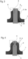
Figure 3 shows a further cross-sectional view of a next step of the manufacturing method, wherein the solder-material was melted and sucked into a gap between the neck and the pin to firmly connect both components. -
Figure 4 shows a further cross-sectional view of an alternative step of the manufacturing method, wherein a welding seam is formed between the neck and the pin. -
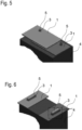
Figure 5 shows a second embodiment of an assembly according to the invention in a perspective view. Two plates are connected to two different cylindrical pins of an electronic device and insulated against each other. -
Figure 6 shows a third embodiment of an assembly according to the invention in a perspective view. Two plates, distanced from each other, are connected to two different cuboid pins of an electronic device. -
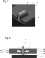
Figure 7 shows an assembly with a cuboid pin in a cross-sectional view. -
Figure 8 shows another embodiment of the assembly, comprising a three-plate busbar. - Similar or apparently identical elements in the figures are marked with the same reference symbols. The figures and the proportions in the figures are not to scale.
-
Figure 1 shows a first embodiment of the invention. It shows aplate 1 with a punchedhole 2 surrounded by aneck 3. Theneck 3 and theplate 1 are formed in one piece. Further,figure 1 shows adevice 4 provided with acylindrical pin 5, wherein thepin 5 is inserted into thehole 2 and the surroundingneck 3. - The diameter of the
hole 2 is preferably between 0.5 mm and 3 mm, more preferably between 1 mm and 1.5 mm. - In a direction vertical to the
plate 1, theneck 3 has preferably a height up to 2.5 mm, preferably between 1.5 mm and 2.5 mm. In particular, the neck comprises a flat section 3a and a round or chamfered section 3b between the flat section 3a of the neck and the planar section of the plate 1 (see alsofigure 2 ). The height of the chamfered section 3b is preferably between more than 0 mm and 1 mm, more preferably between 0.3 and 0.7 mm. The height of the flat section 3a is preferably between 1 mm and 1.5 mm. - The
plate 1 is preferably electrically conductive and comprises or consists of an electrically conductive material, for example an electrically conductive metal or metal alloy, in particular copper (Cu). - In other embodiments, the
plate 1 may comprise other materials or layers which are not electrically conductive, e.g., a substrate supporting the electrically conductive layer. - The
device 4 is preferably an electrical device like, for example, a capacitor, resistor, transistor, inductor, or any otherelectrical device 4. Thedevice 4 comprises the electricallyconductive pin 5 working as an electrical terminal for electrical connection with theplate 1. To connect theplate 1 and thedevice 4, thepin 5 is inserted into thehole 2 and the surroundingneck 3. - Preferably, the neck and the pin positively fit to each other. The neck provides a comparably big connection area. Thus, the surface of the
pin 5 snugs on the inner surface of the neck, particularly the connection area of the neck. - The form-fitting connection between the
pin 5 and theneck 3 provides also mechanical stability of the connection. - As shown in the cross-sectional view of
figure 2 , for building the connection, at first, thepin 5 is inserted into thehole 2. In case of soldering, asolder material 6 may be pre-deposited on an edge 7of the neck. The edge 7shows away from the planar side of the plate. - In a second step, shown in
figure 3 , the solder material is melted by heat and is sucked by the capillary effect into the small gap between the inner surface of theneck 3 and the outer surface of thepin 5. After cooling down, acapillary joint 8 is configured betweenneck 3 andpin 5. - A typical solder material is a material comprising tin or a tin alloy. Thus, the solder material has to be heated up to 230 °C to 240 °C for melting. Advantageously, the applied heat can be punctually applied to the
edge 7 of theneck 3 instead of an edge of theplanar plate 1. Thus, spreading of heat is suppressed and the energy input can be minimized. By a minimized energy input, damage of heat sensitive components like thethin pin 5 or of insulation sheets can be avoided. - To optimize heat requirement, the wall thickness of the
neck 3 is preferably configured smaller than the wall thickness of theplate 1. - Alternatively, the joint may be configured by welding with a welding metal like copper. In this case, the welding temperature has to be higher than the melting temperature of copper, which is 1085 °C. Again, the neck allows advantageously lower heat consumption.
- The welding seam 9 at the
edge 7 is preferably built by laser welding as this method allows very fine structuring of the seam. -
Figure 5 shows a further embodiment according to the invention which is in principle analogous to the first embodiment. - Additional to the first embodiment, the
device 4 of the second embodiment comprises twopins 5, each connected to aplate 1. Theplates 2 are for example metal plates which may work as busbars. The metal plates may comprise copper or a copper alloy. - Between the two overlapping
plates 2, aninsulation sheet 10 is provided, electrically insulating the twoplates 2 against each other. -
Figure 6 shows a third embodiment according to the invention which is in principle analogous to the first and the second embodiment. - However, the embodiment according to
figure 6 shows two main differences. Firstly, thepins 5 are configured rectangular cuboid instead of cylindrical. Secondly, the twoplates 2 do not overlap each other. - The cuboid pins 5 may be elongated in a direction parallel to the
plates 2 as shown infigure 6 to maximize the contact area between thepins 5 and theneck 3. Again, the shape of thenecks 3 is form-fittingly adapted to the shape of thepins 5. The length of thenecks 3 in the elongated direction may amount around 3 to 15 mm, preferably around 5 to 12 mm, more preferably around 8 to 10 mm. -
Figure 7 shows an assembly with a rectangularcuboid pin 5 in a cross-sectional view. Again, theneck 3 is punched out of theplate 1. -
Figure 8 shows an alternative configuration of the assembly, comprising a three-plate busbar 2. The upper and thelower plates 1a are connected to thepin 5, while thecenter plate 1b is insulated from theplates 1a byinsulation sheets 10 and insulated from thepin 5 by avoid gap 11. -
- 1
- plate
- 1a
- lower and upper plate
- 1b
- center plate
- 2
- hole
- 3
- neck
- 3a
- flat section of the neck
- 3b
- chamfered section of the neck
- 4
- electrical device
- 5
- pin
- 6
- solder material
- 7
- edge of the neck
- 8
- capillary joint
- 9
- welding seam
- 10
- insulation sheet
- 11
- void gap
Claims (16)
- Plate (1), which is electrically conductive, comprising a hole (2) surrounded by a neck (3) configured for insertion of an electrically conductive terminal.
- Plate (1) according to claim 1, wherein the neck (3) is formed in one piece with the plate (1).
- Plate (1) according to claim 1 or 2, wherein the plate (1) consists of one or more electrically conductive metals or metal alloys.
- Plate (1) according to any of claims 1 to 3, wherein the plate (1) is a busbar.
- Assembly configured for electrical conduction between the plate (1) according to any of claims 1 to 4 and a pin (5), which is electrically conductive,
wherein the assembly comprises the plate (1) and the pin (5), wherein the pin (5) is inserted into the hole (2) and is electrically connected to the neck (3). - Assembly according to claim 5, wherein the pin (5) has a cylindrical shape or a rectangular cuboid shape.
- Assembly according to claim 5 or 6, wherein the pin (5) consists of one or more electrically conductive metals or metal alloys.
- Assembly according to any of claims 5 to 7, wherein the pin (5) and the neck (3) are firmly connected by solder (6) or by a welding seam (9).
- Assembly according to any of claims 5 to 8, wherein the pin (5) and the neck (3) are form-fittingly connected.
- Assembly according to any of claims 5 to 9, wherein the assembly comprises several plates (1),
wherein the several plates (1) comprising at least one neck (3) each are electrically connected to the pin (5). - Assembly according to any of claims 5 to 10, comprising an electrical device (4) which comprises the one or more pins (5), wherein each pin (5) is electrically connected to one or more of the plates (1).
- Assembly according to claim 11, wherein an insulation sheet (10) is arranged between two adjacent plates (1), which electrically insulates the plates (1) from each other.
- Method for connecting a pin (5) with a plate (1) electrically and mechanically, which are both electrically conductive, comprising the steps- punching a hole (2) in the plate (1), forming a neck (3), which surrounds the hole (2),- inserting the pin (5) into the hole (2) and the surrounding neck (3),- firmly fixing the pin (5) to the neck (3) by means of soldering or welding at an edge (7) of the neck (3) showing away from the plate (1).
- Method according to claim 13, wherein soldering comprises capillary joining (8) between the pin (5) and the neck (3).
- Method according to claim 13 or 14, wherein the solder material (6) is pre-deposited on the edge (7) of the neck (3) before inserting the pin (5) in the hole and the surrounding neck (3).
- Method according to claim 13, wherein welding is performed as laser welding.
Priority Applications (3)
| Application Number | Priority Date | Filing Date | Title |
|---|---|---|---|
| EP23383345.8A EP4576434A1 (en) | 2023-12-21 | 2023-12-21 | Assembly for electrical conduction between a plate and a pin |
| DE202024100643.7U DE202024100643U1 (en) | 2023-12-21 | 2024-02-09 | Arrangement for electrical conduction between a plate and a pin |
| PCT/EP2024/072051 WO2025131344A1 (en) | 2023-12-21 | 2024-08-02 | Assembly for electrical conduction between a plate and a pin |
Applications Claiming Priority (1)
| Application Number | Priority Date | Filing Date | Title |
|---|---|---|---|
| EP23383345.8A EP4576434A1 (en) | 2023-12-21 | 2023-12-21 | Assembly for electrical conduction between a plate and a pin |
Publications (1)
| Publication Number | Publication Date |
|---|---|
| EP4576434A1 true EP4576434A1 (en) | 2025-06-25 |
Family
ID=89535033
Family Applications (1)
| Application Number | Title | Priority Date | Filing Date |
|---|---|---|---|
| EP23383345.8A Pending EP4576434A1 (en) | 2023-12-21 | 2023-12-21 | Assembly for electrical conduction between a plate and a pin |
Country Status (3)
| Country | Link |
|---|---|
| EP (1) | EP4576434A1 (en) |
| DE (1) | DE202024100643U1 (en) |
| WO (1) | WO2025131344A1 (en) |
Citations (3)
| Publication number | Priority date | Publication date | Assignee | Title |
|---|---|---|---|---|
| JPH07241020A (en) * | 1994-02-28 | 1995-09-12 | Yazaki Corp | Electric junction box and manufacturing method thereof |
| JP2005129498A (en) * | 2003-10-01 | 2005-05-19 | Shindengen Electric Mfg Co Ltd | Connection method and structure of busbar and conductive member |
| JP2006179197A (en) * | 2004-12-20 | 2006-07-06 | Toyota Motor Corp | Electronic device bus bar and method for joining connection terminals to electronic device bus bar |
-
2023
- 2023-12-21 EP EP23383345.8A patent/EP4576434A1/en active Pending
-
2024
- 2024-02-09 DE DE202024100643.7U patent/DE202024100643U1/en active Active
- 2024-08-02 WO PCT/EP2024/072051 patent/WO2025131344A1/en active Pending
Patent Citations (3)
| Publication number | Priority date | Publication date | Assignee | Title |
|---|---|---|---|---|
| JPH07241020A (en) * | 1994-02-28 | 1995-09-12 | Yazaki Corp | Electric junction box and manufacturing method thereof |
| JP2005129498A (en) * | 2003-10-01 | 2005-05-19 | Shindengen Electric Mfg Co Ltd | Connection method and structure of busbar and conductive member |
| JP2006179197A (en) * | 2004-12-20 | 2006-07-06 | Toyota Motor Corp | Electronic device bus bar and method for joining connection terminals to electronic device bus bar |
Also Published As
| Publication number | Publication date |
|---|---|
| WO2025131344A1 (en) | 2025-06-26 |
| DE202024100643U1 (en) | 2024-05-22 |
Similar Documents
| Publication | Publication Date | Title |
|---|---|---|
| JP3212318U (en) | Connection member, connection assembly, battery module support assembly, and battery module | |
| US7331799B1 (en) | Stacked electronic component and fastening device thereof | |
| KR101096281B1 (en) | Battery pack | |
| US5214563A (en) | Thermally reactive lead assembly and method for making same | |
| US7568958B2 (en) | Electrical terminal for sealed accumulator | |
| US9508519B2 (en) | Fuse and manufacturing method thereof | |
| US20220199346A1 (en) | Protective element | |
| CN101677151A (en) | Electronic component with lead wire | |
| JPH0318010A (en) | Capacitor with fuse | |
| JP6715583B2 (en) | Welding and soldering of transistor leads | |
| JP2011113676A (en) | Connection method of terminal to flexible flat cable and terminal | |
| TWI416549B (en) | Ptc device and electric apparatus including the same | |
| WO2025131344A1 (en) | Assembly for electrical conduction between a plate and a pin | |
| US7439625B2 (en) | Circuit board | |
| CN104115244B (en) | Electronic component and method for manufacturing same | |
| JP2000164093A (en) | Thermal fuse and manufacturing method thereof | |
| EP4057785A1 (en) | Busbar and method for manufacturing a busbar | |
| CN101630647B (en) | Welding method and welding structure of conductive terminals | |
| JP2003092025A (en) | Flexible conductor and compression type copper tube terminal | |
| CN215377361U (en) | Melt structure | |
| EP3819650B1 (en) | Current detection device and manufacturing method thereof | |
| US10667409B2 (en) | Contacting arrangement and method for forming the contacting arrangement | |
| JP2002208788A (en) | Circuit board and its manufacturing method | |
| KR20260061908A (en) | Aluminum Laminated shunt and method for manufacturing thereof | |
| US20250198853A1 (en) | Flexible sensor unit for measuring temperature at power contacts for e-mobility |
Legal Events
| Date | Code | Title | Description |
|---|---|---|---|
| PUAI | Public reference made under article 153(3) epc to a published international application that has entered the european phase |
Free format text: ORIGINAL CODE: 0009012 |
|
| STAA | Information on the status of an ep patent application or granted ep patent |
Free format text: STATUS: REQUEST FOR EXAMINATION WAS MADE |
|
| 17P | Request for examination filed |
Effective date: 20240829 |
|
| AK | Designated contracting states |
Kind code of ref document: A1 Designated state(s): AL AT BE BG CH CY CZ DE DK EE ES FI FR GB GR HR HU IE IS IT LI LT LU LV MC ME MK MT NL NO PL PT RO RS SE SI SK SM TR |