EP4576419A1 - Apparatus and method for differential signal routing - Google Patents
Apparatus and method for differential signal routing Download PDFInfo
- Publication number
- EP4576419A1 EP4576419A1 EP23219044.7A EP23219044A EP4576419A1 EP 4576419 A1 EP4576419 A1 EP 4576419A1 EP 23219044 A EP23219044 A EP 23219044A EP 4576419 A1 EP4576419 A1 EP 4576419A1
- Authority
- EP
- European Patent Office
- Prior art keywords
- pair
- path
- paths
- coupling
- parallel
- Prior art date
- Legal status (The legal status is an assumption and is not a legal conclusion. Google has not performed a legal analysis and makes no representation as to the accuracy of the status listed.)
- Pending
Links
Images




Classifications
-
- H—ELECTRICITY
- H01—ELECTRIC ELEMENTS
- H01P—WAVEGUIDES; RESONATORS, LINES, OR OTHER DEVICES OF THE WAVEGUIDE TYPE
- H01P3/00—Waveguides; Transmission lines of the waveguide type
- H01P3/02—Waveguides; Transmission lines of the waveguide type with two longitudinal conductors
- H01P3/026—Coplanar striplines [CPS]
-
- H—ELECTRICITY
- H01—ELECTRIC ELEMENTS
- H01P—WAVEGUIDES; RESONATORS, LINES, OR OTHER DEVICES OF THE WAVEGUIDE TYPE
- H01P5/00—Coupling devices of the waveguide type
- H01P5/12—Coupling devices having more than two ports
- H01P5/16—Conjugate devices, i.e. devices having at least one port decoupled from one other port
-
- H—ELECTRICITY
- H01—ELECTRIC ELEMENTS
- H01P—WAVEGUIDES; RESONATORS, LINES, OR OTHER DEVICES OF THE WAVEGUIDE TYPE
- H01P3/00—Waveguides; Transmission lines of the waveguide type
- H01P3/02—Waveguides; Transmission lines of the waveguide type with two longitudinal conductors
- H01P3/08—Microstrips; Strip lines
-
- H—ELECTRICITY
- H01—ELECTRIC ELEMENTS
- H01P—WAVEGUIDES; RESONATORS, LINES, OR OTHER DEVICES OF THE WAVEGUIDE TYPE
- H01P5/00—Coupling devices of the waveguide type
- H01P5/12—Coupling devices having more than two ports
-
- H—ELECTRICITY
- H05—ELECTRIC TECHNIQUES NOT OTHERWISE PROVIDED FOR
- H05K—PRINTED CIRCUITS; CASINGS OR CONSTRUCTIONAL DETAILS OF ELECTRIC APPARATUS; MANUFACTURE OF ASSEMBLAGES OF ELECTRICAL COMPONENTS
- H05K1/00—Printed circuits
- H05K1/02—Details
- H05K1/0213—Electrical arrangements not otherwise provided for
- H05K1/0237—High frequency adaptations
- H05K1/0245—Lay-out of balanced signal pairs, e.g. differential lines or twisted lines
Definitions
- the invention relates to differential signal distribution, especially to splitter or combiner networks for routing high frequency, for example Radio Frequency (RF),differential signals.
- RF Radio Frequency
- the differential signal branching from the central point of symmetry to multiple signal tapping networks, must be carefully laid out to maintain symmetry.
- the symmetrical distribution of wiring requires that the electrical length of the signal lines must always be identical in the two parts, i.e., the positive signal path and the negative signal path, of the differential path, and the capacitive coupling, e.g., to other lines or to the substrate, must be as similar as possible in the two parts of the differential path.
- US 2011/0032065 A1 discloses a symmetrical transformer for differential signaling.
- a disadvantage of US 2011/0032065 A1 is that a symmetrical distribution of wiring is not utilized for routing the differential signal to or from the symmetrical transformer, which may affect the signal integrity in terms of imbalance between positive and negative signals.
- an object of the invention is to provide an apparatus and a method for improving the signal integrity in terms of imbalance between positive and negative signals lines of a differential signal line.
- an apparatus for differential signal routing comprises a first network comprising a first pair of parallel distribution paths having substantially identical lengths and widths realized on a first metal routing layer, a second pair of parallel distribution paths having substantially identical lengths and widths realized on the first metal routing layer, and a first pair of parallel routing paths having substantially identical lengths and widths realized on a second metal routing layer being orthogonal to the first metal routing layer.
- one path of the first pair of parallel routing paths is connected to one path of the first pair of parallel distribution paths via a first coupling path comprising a first vertical interconnect access and further to one path of the second pair of parallel distribution paths via a second coupling path comprising a second vertical interconnect access in order to combine or split signals coming from or between the one path of the first pair of parallel distribution paths and the one path of the second pair of parallel distribution paths, respectively.
- other path of the first pair of parallel routing paths is connected to other path of the first pair of parallel distribution paths via a third coupling path comprising a third vertical interconnect access and further to other path of the second pair of parallel distribution paths via a fourth coupling path comprising a fourth vertical interconnect access in order to combine or split signals coming from or between the other path of the first pair of parallel distribution paths and the other path of the second pair of parallel distribution paths, respectively.
- At least the first coupling path and the third coupling path have substantially identical lengths and widths
- at least the second coupling path and the fourth coupling path have substantially identical lengths and widths.
- the first metal routing layer and the second metal routing layer correspond to back-end-of-line (BEOL) metallization structures.
- BEOL back-end-of-line
- the BEOL metallization structure may be a part of an integrated circuit, especially comprising semiconductor based wafers with planar layers.
- the integrated circuit may further comprise a front-end-of-line (FEOL) with active devices, such as transistors, and the BEOL for signal routing.
- FEOL front-end-of-line
- the first metal routing layer and the second metal routing layer may be adjacent metal layers or levels of the planar integrated circuit BEOL metallization structure.
- each of the vertical interconnect accesses may provide a vertical electrically conductive connection between the first metal routing layer and the second metal routing layer, thereby electrically connecting the first metal routing layer to the second metal routing layer.
- the first metal routing layer and the second metal routing layer may not be adjacent metal layers or levels of the planar integrated circuit BEOL metallization structure.
- each of the vertical interconnect accesses may provide a vertical electrically conductive connection between the first metal routing layer and the second metal routing layer covering more layers, this is achieved by super-VIA's as known to the skilled person in the art. The super-VIA thereby electrically connecting the first metal routing layer to the non adjacent second metal routing layer.
- the vertical interconnect accesses are vertically connecting the metal layer which are in a horizontal plane. So the vertical interconnect accesses are orthogonal and upward/downward oriented with respect to the metal layers.
- each of the first coupling path and the third coupling path comprises a number of turns identical to each other.
- each of the second coupling path and the fourth coupling path comprises a number of turns identical to each other.
- the first coupling path, the second coupling path, the third coupling path, and the fourth coupling path have substantially identical lengths and widths, and identical number of turns.
- the symmetry between the positive signal path and the negative signal path for each of the first pair of parallel distribution paths and the second pair of parallel distribution paths can be maintained.
- the first coupling path, the second coupling path, the third coupling path, and the fourth coupling path have identical number of 45 degrees turns.
- the number of turns for each of the coupling paths may be identical to each other.
- the number of turns may comprise one or more turns between 40 degrees and 50 degrees, preferably between 42 degrees and 48 degrees, more preferably between 44 degrees and 46 degrees, most preferably one or more 45 degrees turns.
- the first coupling path, the second coupling path, the third coupling path, and the fourth coupling path have identical number of 90 degrees turns.
- the number of turns for each of the coupling paths may be identical to each other.
- the number of turns may comprise one or more turns between 85 degrees and 95 degrees, preferably between 87 degrees and 93 degrees, more preferably between 89 degrees and 91 degrees, most preferably one or more 90 degrees turns.
- the number of turns may comprise one or more 22.5 degrees turns or other polygon shapes.
- the one path of the first pair of parallel routing paths and the first pair of parallel distribution paths overlap at their respective cross-sections.
- the other path of the first pair of parallel routing paths and the second pair of parallel distribution paths overlap at their respective cross-sections.
- the one path of the first pair of parallel routing paths and the first pair of parallel distribution paths may overlap at their respective cross-sections such that both the positive signal path and the negative signal path may operate with similar amount of capacitive coupling between them, e.g., formed at their respective cross-sections.
- the other path of the first pair of parallel routing paths and the second pair of parallel distribution paths may overlap at their respective cross-sections such that both the positive signal path and the negative signal path may operate with similar amount of capacitive coupling between them, e.g., formed at their respective cross-sections.
- the apparatus further comprises at least one second network.
- the second network comprises a second pair of parallel routing paths having substantially identical lengths and widths realized on the second metal routing layer, and a pair of vertical interconnect accesses being symmetrically arranged on the first metal routing layer with respect to the lengths of the first pair of parallel distribution paths or the second pair of parallel distribution paths, wherein each vertical interconnect access of the pair of vertical interconnect accesses is arranged on a respective distribution path of the first pair of parallel distribution paths or the second pair of parallel distribution paths.
- the second pair of parallel routing paths are respectively connected to the pair of vertical interconnect accesses via a pair of coupling paths having substantially identical lengths and widths realized on the second metal routing layer, the pair of coupling paths being symmetrically connected to the second pair of parallel routing paths with respect to the lengths of the second pair of parallel routing paths in order to couple in or out a differential signal to or from the first pair of parallel distribution paths or the second pair of parallel distribution paths, respectively.
- an imbalance between the positive signal and the negative signal of a differential signal can be drastically reduced by utilizing extreme symmetry between the positive signal path and the negative signal path, thereby improving the signal integrity.
- the second network allows to make a 90 degrees turn in both of the differential signal paths.
- the widths of the second pair of parallel routing paths and the widths of the pair of coupling paths are substantially identical to each other.
- the widths of the second pair of parallel routing paths and the widths of the pair of coupling paths are different from each other.
- the different coupling paths can be formed in a flexible manner within the design rule, e.g., to meet a certain area constraint, whereby maintain the symmetry between the positive signal path and the negative signal path.
- each path of the pair of coupling paths comprises a number of turns identical to each other, especially a number of 45 degrees turns.
- the number of turns for each of the coupling paths may be identical to each other.
- the number of turns may comprise one or more turns between 40 degrees and 50 degrees, preferably between 42 degrees and 48 degrees, more preferably between 44 degrees and 46 degrees, most preferably one or more 45 degrees turns.
- each path of the pair of coupling paths comprises a number of turns identical to each other, especially a number of 90 degrees turns.
- the number of turns for each of the coupling paths may be identical to each other.
- the number of turns may comprise one or more turns between 85 degrees and 95 degrees, preferably between 87 degrees and 93 degrees, more preferably between 89 degrees and 91 degrees, most preferably one or more 90 degrees turns.
- the number of turns may comprise one or more 22.5 degrees turns or other polygon shapes.
- the second pair of parallel routing paths and the first pair of parallel distribution paths or the second pair of parallel distribution paths overlap at their respective cross-sections.
- the second pair of parallel routing paths and the first pair of parallel distribution paths, or the second pair of parallel routing paths and the second pair of parallel distribution paths may overlap at their respective cross-sections such that both the positive signal path and the negative signal path may operate with similar amount of capacitive coupling, e.g., formed at their respective cross-sections.
- a method for differential signal routing.
- the method comprises a step of forming a first pair of parallel distribution paths having substantially identical lengths and widths on a first metal routing layer.
- the method further comprises a step of forming a second pair of parallel distribution paths having substantially identical lengths and widths on the first metal routing layer.
- the method comprises a step of forming a first pair of parallel routing paths having substantially identical lengths and widths realized on a second metal routing layer being orthogonal to the first metal routing layer.
- the method further comprises a step of connecting one path of the first pair of parallel routing paths to one path of the first pair of parallel distribution paths via a first coupling path comprising a first vertical interconnect access and further to one path of the second pair of parallel distribution paths via a second coupling path comprising a second vertical interconnect access.
- the method comprises a step of connecting other path of the first pair of parallel routing paths to other path of the first pair of parallel distribution paths via a third coupling path comprising a third vertical interconnect access and further to other path of the second pair of parallel distribution paths via a fourth coupling path comprising a fourth vertical interconnect access.
- the method comprises a step of combining or splitting signals coming from or between the one path of the first pair of parallel distribution paths and the one path of the second pair of parallel distribution paths, respectively, by the one path of the first pair of parallel routing paths.
- the method comprises a step of combining or splitting signals coming from or between the other path of the first pair of parallel distribution paths and the other path of the second pair of parallel distribution paths, respectively, by the other path of the first pair of parallel routing paths.
- the method further comprises a step of forming a second pair of parallel routing paths having substantially identical lengths and widths on the second metal routing layer.
- the method comprises a step of symmetrically arranging a pair of vertical interconnect accesses on the first metal routing layer with respect to the lengths of the first pair of parallel distribution paths or the second pair of parallel distribution paths such that each vertical interconnect access of the pair of vertical interconnect accesses is arranged on a respective distribution path of the first pair of parallel distribution paths or the second pair of parallel distribution paths.
- the method comprises a step of forming a pair of coupling paths having substantially identical lengths and widths on the second metal routing layer such that the pair of coupling paths being symmetrically connected to the second pair of parallel routing paths with respect to the lengths of the second pair of parallel routing paths.
- the method comprises a step of respectively connecting the second pair of parallel routing paths to the pair of vertical interconnect accesses via the pair of coupling paths in order to couple in or out a differential signal to or from the first pair of parallel distribution paths or the second pair of parallel distribution paths, respectively.
- substantially identical can be understood as having an identical property between multiple entities.
- the term “substantially identical” can be understood as having a property with a difference less than 10%, preferably less than 5%, more preferably less than 2%, most preferably less than 1% between multiple entities.
- the method according to the second aspect corresponds to the apparatus according to the first aspect and its implementation forms. Accordingly, the method of the second aspect may have corresponding implementation forms. Further, the method of the second aspect achieves the same advantages and effects as the apparatus of the first aspect and its respective implementation forms.
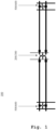
- the apparatus 100 may correspond to a signal splitter or a signal combiner for splitting or combining differential signals, respectively.
- the apparatus 100 may comprise a central network 200, 300 for splitting a differential signal onto two differential signal transmission lines or for combining differential signals coming from the two differential signal transmission lines.
- the apparatus 100 may further comprise two corner networks 500, 600 for routing the differential signals from the respective differential signal transmission lines, e.g., to or from a respective load. It is to be noted that the number of corner networks 500, 600 can be less than or more than two.
- the central network 200, 300 may be arranged to facilitate a central point of symmetry with respect to the corner splitters 500, 600, and symmetrical interconnection for the corner splitters 500, 600 from the central point of symmetry may be maintained to achieve an equivalent electrical length, width, and capacitive coupling in the respective positive and the negative paths of the differential signal transmission lines.
- a first exemplary embodiment of the first network 200 according to the first aspect of the invention is illustrated.
- the first network 200 may correspond to the central network of Fig. 1 .
- the first network 200 may comprise a first pair of distribution paths comprising a first path 201 1 and a second path 201 2 , e.g., one for the positive signal (p-path) and the other for the negative signal (n-path) of the differential signal.
- the first path 201 1 and the second path 201 2 of the first pair of distribution paths may have identical lengths and widths.
- each of the first path 201 1 and the second path 201 2 of the first pair of distribution paths may correspond to the length or horizontal distance between the central network and one of the corner networks of Fig. 1 , e.g., between the respective signal tapping points, to achieve symmetry in the horizontal signal distribution.
- the first path 201 1 and the second path 201 2 of the first pair of distribution paths may be realized on a first (M1) metal routing layer.
- the first network 200 may comprise a second pair of distribution paths comprising a first path 202 1 and a second path 202 2 , e.g., one for the positive signal (p-path) and the other for the negative signal (n-path) of the differential signal.
- the first path 202 1 and the second path 202 2 of the second pair of distribution paths may have identical lengths and widths.
- each of the first path 202 1 and the second path 202 2 of the second pair of distribution paths may correspond to the length or horizontal distance between the central network and one of the corner networks of Fig. 1 , e.g., between the respective signal tapping points, to achieve symmetry in the horizontal signal distribution.
- the first path 202 1 and the second path 202 2 of the second pair of distribution paths may be realized on the M1 metal routing layer.
- the first network 200 may comprise a pair of routing paths comprising a first path 203 1 and a second path 203 2 , e.g., one for the positive signal (p-path) and the other for the negative signal (n-path) of the differential signal.
- the first path 203 1 and the second path 203 2 of the pair of routing paths may have identical lengths and widths.
- the first path 203 1 and the second path 203 2 of the pair of routing paths may be realized on a second (M2) metal routing layer.
- the M2 metal routing direction of the M2 routing layer may be orthogonal to the M1 metal routing direction of the M1 routing layer.
- This orthogonality is in the horizontal plane in which the metal layers are formed in for example integrated circuits (IC), more particularly CMOS IC's.
- IC integrated circuits
- the coupling paths are not restricted to the orthogonal restriction of the routing direction.
- the coupling paths may comprise turns of 22.5, 45 or 90 degrees. Further the coupling paths may also comprise polygon shapes of other and multiple angles forming curves or bends if the integration technology allow for that.
- the M1 metal routing layer and the M2 metal routing layer may be adjacent metal routing layers.
- the first and second metal layers can be interchanged.
- the first and second metal layers may be layers with other metal layers in between the first and second metal layers.
- the vertical interconnect accesses are covering multiple metal layers to cover the distance between the first and the second layer, this is achieved by so called super-VIA's, which are known in the art.
- the VIA's or super-VIA's are vertical interconnect structures so are orthogonal to the plane of the metal layers in planar integration technologies for fabricating IC's.
- first path 203 1 of the pair of routing paths may be connected to the first path 201 1 of the first pair of distribution paths via a first coupling path 204 1 .
- a first vertical interconnect access (VIA) 205 1 may be arranged on the first coupling path 204 1 to vertically connect the M1 metal routing layer and the M2 metal routing layer, thereby interconnecting the first path 203 1 of the pair of routing paths and the first path 201 1 of the first pair of distribution paths.
- the first coupling path 204 1 may comprise four successive 45 degrees turns. However, the first coupling path 204 1 may comprise more than or less than four 45 degrees turns. Alternatively, the first coupling path 204 1 may comprise a number of successive 22.5 degrees turns. Alternatively, the first coupling path 204 1 may be realized in any polygon shapes that can be achieved within the design rule.
- first path 203 1 of the pair of routing paths may be further connected to the first path 202 1 of the second pair of distribution paths via a second coupling path 204 2 .
- a second VIA 205 2 may be arranged on the second coupling path 204 2 to vertically connect the M1 metal routing layer and the M2 metal routing layer, thereby interconnecting the first path 203 1 of the pair of routing paths and the first path 202 1 of the second pair of distribution paths.
- the second coupling path 204 2 may comprise four successive 45 degrees turns. However, the second coupling path 204 2 may comprise more than or less than four 45 degrees turns. Alternatively, the second coupling path 204 2 may comprise a number of successive 22.5 degrees turns. Alternatively, the second coupling path 204 2 may be realized in any polygon shapes that can be achieved within the design rule.
- the first path 203 1 of the pair of routing paths may combine or split signals coming from or between the first path 201 1 of the first pair of distribution paths and the first path 202 1 of the second pair of distribution paths, respectively.
- the third coupling path 204 3 may comprise four successive 45 degrees turns. However, the third coupling path 204 3 may comprise more than or less than four 45 degrees turns. Alternatively, the third coupling path 204 3 may comprise a number of successive 22.5 degrees turns.
- the third coupling path 204 3 may be realized in any polygon shapes that can be achieved within the design rule.
- the second path 203 2 of the pair of routing paths may be further connected to the second path 202 2 of the second pair of distribution paths via a fourth coupling path 204 4 .
- a fourth VIA 205 4 may be arranged on the fourth coupling path 204 4 to vertically connect the M1 metal routing layer and the M2 metal routing layer, thereby interconnecting the second path 203 2 of the pair of routing paths and the second path 202 2 of the second pair of distribution paths.
- the fourth coupling path 204 4 may comprise four successive 45 degrees turns. However, the fourth coupling path 204 4 may comprise more than or less than four 45 degrees turns. Alternatively, the fourth coupling path 204 4 may comprise a number of successive 22.5 degrees turns. Alternatively, the fourth coupling path 204 4 may be realized in any polygon shapes.
- the second path 203 2 of the pair of routing paths may combine or split signals coming from or between the second path 201 2 of the first pair of distribution paths and the second path 202 2 of the second pair of distribution paths, respectively.
- the first coupling path 204 1 and the third coupling path 204 3 may have identical lengths, identical widths, identical number of turns, and/or identical polygon shapes.
- the second coupling path 204 2 and the fourth coupling path 204 4 may have identical lengths, identical widths, identical number of turns, and/or identical polygon shapes.
- first coupling path 204 1 , the second coupling path 204 2 , the third coupling path 204 3 , and the fourth coupling path 204 4 may have identical lengths, identical widths, identical number of turns, and/or identical polygon shapes.
- the first coupling path 204 1 may comprise a first portion 207 1 realized on the M2 metal layer being connected to the first path 203 1 of the pair of routing paths.
- the first coupling path 204 1 may further comprise a second portion 207 2 realized on the M1 metal layer being connected to the first path 201 1 of the first pair of distribution paths.
- the first VIA 205 1 may interconnect the first portion 207 1 and the second portion 207 2 of the first coupling path 204 1 .
- the second coupling path 204 2 may be realized on the M2 metal layer being connected to the first path 203 1 of the pair of routing paths, e.g., forming a common branching point for both the first coupling path 204 1 and the second coupling path 204 2 from the first path 203 1 of the pair of routing paths.
- the second VIA 205 2 may interconnect the second coupling path 204 2 and the first path 202 1 of the second pair of distribution paths.
- the third coupling path 204 3 may comprise a first portion 208 1 realized on the M2 metal layer being connected to the second path 203 2 of the pair of routing paths.
- the third coupling path 204 3 may further comprise a second portion 208 2 realized on the M1 metal layer being connected to the second path 201 2 of the first pair of distribution paths.
- the third VIA 205 3 may interconnect the first portion 208 1 and the second portion 208 2 of the third coupling path 204 3 .
- the fourth coupling path 204 4 may be realized on the M2 metal layer being connected to the second path 203 2 of the pair of routing paths, e.g., forming a common branching point for both the third coupling path 204 3 and the fourth coupling path 204 4 from the second path 203 2 of the pair of routing paths.
- the fourth VIA 205 4 may interconnect the fourth coupling path 204 4 and the second path 202 2 of the second pair of distribution paths.
- the common branching point on the first path 203 1 of the pair of routing paths and the common branching point on the second path 203 2 of the pair of routing paths may be realized in a symmetrical manner with respect to the lengths of the pair of routing paths, i.e., at a distance along the length of each path of the pair of routing paths that is equivalent or identical to each other.
- first path 203 1 of the pair of routing paths and the first path 201 1 of the first pair of distribution paths may overlap at a first cross-section 206 1 .
- second path 203 2 of the pair of routing paths and the first path 202 1 of the second pair of distribution paths may overlap at a second cross-section 206 2 .
- first path 203 1 of the pair of routing paths and the second path 201 2 of the first pair of distribution paths may overlap at a third cross-section 206 3 .
- second path 203 2 of the pair of routing paths and the second path 202 2 of the second pair of distribution paths may overlap at a fourth cross-section 206 4 .
- the first path 203 1 of the pair of routing paths and the first path 201 1 of the first pair of distribution paths may operate in-phase, which may result in the coupling capacitance between two in-phase signals.
- the second path 203 2 of the pair of routing paths and the first path 202 1 of the second pair of distribution paths may operate in antiphase, which may result in the coupling capacitance between two antiphase signals.
- the first path 203 1 of the pair of routing paths and the second path 201 2 of the first pair of distribution paths may operate in antiphase, which may result in the coupling capacitance between two antiphase signals.
- the second path 203 2 of the pair of routing paths and the second path 202 2 of the second pair of distribution paths may operate in-phase, which may result in the coupling capacitance between two in-phase signals.
- the differential signal path from the first path 203 1 of the pair of routing paths to the first path 201 1 of the first pair of distribution paths via the first coupling path 204 1 and the differential signal path from the second path 203 2 of the pair of routing paths to the second path 201 2 of the first pair of distribution paths via the third coupling path 204 3 may experience an equivalent electrical length, width, line inductance, and an equivalent amount of coupling capacitance.
- the differential signal path from the first path 203 1 of the pair of routing paths to the first path 202 1 of the second pair of distribution paths via the second coupling path 204 2 and the differential signal path from the second path 203 2 of the pair of routing paths to the second path 202 2 of the second pair of distribution paths via the fourth coupling path 204 4 may experience an equivalent electrical length, width, line inductance, and an equivalent amount of coupling capacitance.
- a second exemplary embodiment of the first network 300 according to the first aspect of the invention is illustrated.
- the first network 300 may correspond to the central network of Fig. 1 .
- the first network 300 may differ from the first network 200 in that the first coupling path 304 1 , the second coupling path 304 2 , the third coupling path 304 3 , and the fourth coupling path 304 4 may have a number of consecutive 90 degrees turns.
- the first coupling path 304 1 may comprise a first portion 307 1 realized on the M2 metal layer (shown as darker grayscale) by extending the first path 203 1 of the pair of routing paths.
- the first coupling path 304 1 may further comprise a second portion 307 2 realized on the M1 metal layer (shown as lighter grayscale) being extended from the first path 201 1 of the first pair of distribution paths.
- the first VIA 205 1 may interconnect the first portion 307 1 and the second portion 307 2 of the first coupling path 304 1 .
- the second coupling path 304 2 may be realized on the M2 metal layer by extending the first path 203 1 of the pair of routing paths, e.g., forming a common branching point for both the first coupling path 304 1 and the second coupling path 304 2 at the first VIA 205 1 .
- the second VIA 205 2 may interconnect the second coupling path 304 2 and the first path 202 1 of the second pair of distribution paths.
- the third coupling path 304 3 may comprise a first portion 308 1 realized on the M2 metal layer by extending the second path 203 2 of the pair of routing paths.
- the third coupling path 304 3 may further comprise a second portion 308 2 realized on the M1 metal layer being extended from the second path 201 2 of the first pair of distribution paths.
- the third VIA 205 3 may interconnect the first portion 308 1 and the second portion 308 2 of the third coupling path 304 3 .
- the fourth coupling path 304 4 may be realized on the M2 metal layer by extending the second path 203 2 of the pair of routing paths, e.g., forming a common branching point for both the third coupling path 304 3 and the fourth coupling path 304 4 at the third VIA 205 3 .
- the fourth VIA 405 4 may interconnect the fourth coupling path 304 4 and the second path 202 2 of the second pair of distribution paths.
- the first coupling path 304 1 and the third coupling path 304 3 may have identical lengths, identical widths, identical number of turns, and/or identical shapes.
- the second coupling path 304 2 and the fourth coupling path 304 4 may have identical lengths, identical widths, identical number of turns, and/or identical shapes.
- first coupling path 304 1 , the second coupling path 304 2 , the third coupling path 304 3 , and the fourth coupling path 304 4 may have identical lengths, identical widths, identical number of turns, and/or identical shapes.
- first portion 307 1 and the second portion 307 2 of the first coupling path 304 1 may overlap at a first cross-section 306 1 .
- second portion 307 2 of the first coupling path 304 1 and the fourth coupling path 304 4 may overlap at a second cross-section 306 2 .
- the second coupling path 304 2 and the second portion 308 2 of the third coupling path 304 3 may overlap at a third cross-section 306 3 .
- first portion 308 1 of the third coupling path 304 3 and the fourth coupling path 304 4 may overlap at a fourth cross-section 306 4 .
- the crossed-over paths may operate in-phase, which may result in the coupling capacitance between two in-phase signals.
- the crossed-over paths may operate in antiphase, which may result in the coupling capacitance between two antiphase signals.
- the crossed-over paths may operate in antiphase, which may result in the coupling capacitance between two antiphase signals.
- the crossed-over paths may operate in-phase, which may result in the coupling capacitance between two in-phase signals.
- the differential signal path from the first path 203 1 of the pair of routing paths to the first path 201 1 of the first pair of distribution paths via the first coupling path 304 1 and the differential signal path from the second path 203 2 of the pair of routing paths to the second path 201 2 of the first pair of distribution paths via the third coupling path 304 3 may experience an equivalent electrical length, width, line inductance, and an equivalent amount of coupling capacitance.
- the differential signal path from the first path 203 1 of the pair of routing paths to the first path 202 1 of the second pair of distribution paths via the second coupling path 304 2 and the differential signal path from the second path 203 2 of the pair of routing paths to the second path 202 2 of the second pair of distribution paths via the fourth coupling path 304 4 may experience an equivalent electrical length, width, line inductance, and an equivalent amount of coupling capacitance.
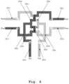
- Fig. 4 an exemplary signal flow for the network 300 is illustrated.
- a split operation of a differential signal Pin, Nin from the pair of routing paths 203 1 , 203 2 to the first pair of distribution paths 201 1 , 201 2 and the second pair of distribution path 202 1 , 202 2 is illustrated.
- the p-path is shown in the darker grayscale and the n-path is shown in the lighter grayscale.
- the positive signal Pin may be inputted from the first path 203 1 of the pair of routing paths and may be split between the first path 201 1 of the first pair of distribution paths and the first path 202 1 of the second pair of distribution paths (shown as Pout).
- the negative signal Nin may be inputted from the second path 203 2 of the pair of routing paths and may be split between the second path 201 2 of the first pair of distribution paths and the second path 202 2 of the second pair of distribution paths (shown as Nout).
- the signal path Pin-Pout from the first path 203 1 of the pair of routing paths to the first path 201 1 of the first pair of distribution paths and the signal path Nin-Nout from the second path 203 2 of the pair of routing paths to the second path 201 2 of the first pair of distribution paths may experience an equivalent electrical length, width, line inductance, and an equivalent amount of coupling capacitance.
- the signal path Pin-Pout from the first path 203 1 of the pair of routing paths to the first path 202 1 of the second pair of distribution paths and the signal path Nin-Nout from the second path 203 2 of the pair of routing paths to the second path 202 2 of the second pair of distribution paths may experience an equivalent electrical length, width, line inductance, and an equivalent amount of coupling capacitance.
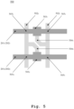
- a first exemplary embodiment of the second network 500 according to the first aspect of the invention is illustrated.
- the second network 500 may correspond to the corner network of Fig. 1 .
- the second network 500 may comprise a pair of distribution paths.
- the pair of distribution paths may correspond to the first pair of distribution paths 201 1 , 201 2 or the second pair of distribution paths 202 1 , 202 2 of the first network 200, 300 as shown in Fig. 2 to Fig. 4 . It is to be noted, in the following, only the first pair of distribution paths 201 1 , 201 2 is considered, and the implementation is analogous for the second pair of distribution paths 202 1 , 202 2 .
- the pair of distribution paths may comprise the first path 201 1 and the second path 201 2 , e.g., one for the positive signal (p-path) and the other for the negative signal (n-path) of the differential signal, which may have identical lengths and widths.
- each of the first path 201 1 and the second path 201 2 of the pair of distribution paths may correspond to the length or horizontal distance between the central network and one of the corner networks of Fig. 1 , e.g., between the respective signal tapping points, to achieve symmetry in the horizontal signal distribution.
- first path 201 1 and the second path 201 2 of the pair of distribution paths may be realized on the M1 metal routing layer.
- the second network 500 may comprise a pair of routing paths comprising a first path 502 1 and a second path 502 2 , e.g., one for the positive signal (p-path) and the other for the negative signal (n-path) of the differential signal.
- the first path 502 1 and the second path 502 2 of the pair of routing paths may have identical lengths and widths.
- the first path 502 1 and the second path 502 2 of the pair of routing paths may be realized on the M2 metal routing layer.
- the signal routing direction of the signal paths in the M2 metal routing layer may be orthogonal to the signal routing direction of the signal paths in the M1 metal routing layer.
- the M1 metal routing layer and the M2 metal routing layer may be adjacent metal routing layers.
- the first path 502 1 of the pair of routing paths may be connected to the first path 201 1 of the pair of distribution paths via a first coupling path 504 1 .
- the first coupling path 504 1 may be realized on the M2 metal routing layer being connected to the first path 502 1 of the pair of routing paths and further to the first path 201 1 of the pair of distribution paths through a first VIA 503 1 .
- the first VIA 503 1 may be arranged on the first path 201 1 of the pair of distribution paths to vertically connect the M1 metal routing layer and the M2 metal routing layer, thereby interconnecting the first coupling path 504 1 and the first path 201 1 of the pair of distribution paths.
- the second path 502 2 of the pair of routing paths may be connected to the second path 201 2 of the pair of distribution paths via a second coupling path 504 2 .
- the second coupling path 504 2 may be realized on the M2 metal routing layer being connected to the second path 502 2 of the pair of routing paths and further to the second path 201 2 of the pair of distribution paths through a second VIA 503 2 .
- the second VIA 503 2 may be arranged on the second path 201 2 of the pair of distribution paths to vertically connect the M1 metal routing layer and the M2 metal routing layer, thereby interconnecting the second coupling path 504 2 and the second path 201 2 of the first of distribution paths.
- the first path 502 1 of the pair of routing paths may route a signal to or from the first path 201 1 of the pair of distribution paths via the first coupling path 504 1 and the second path 502 2 of the pair of routing paths may route a signal to or from the second path 201 2 of the pair of distribution paths via the second coupling path 504 2 .
- first coupling path 504 1 and the second coupling path 504 2 may be connected to the first path 502 1 of the pair of routing paths and the second path 502 2 of the pair of routing paths, respectively, at points symmetrical to each other, i.e., at a distance along the length of each path of the pair of routing paths that is equivalent or identical to each other.
- first VIA 503 1 and the second VIA 503 2 may be arranged on the first path 201 1 of the pair of distribution paths and the second path 201 2 of the pair of distribution paths, respectively, at points symmetrical to each other, i.e., at a distance along the length of each path of the pair of distribution paths that is equivalent or identical to each other.
- the first coupling path 504 1 may comprise two successive 45 degrees turns. However, the first coupling path 504 1 may comprise more than or less than two 45 degrees turns. Alternatively, the first coupling path 504 1 may comprise a number of successive 22.5 degrees turns. Alternatively, the first coupling path 504 1 may be realized in any polygon shapes that can be achieved within the design rule.
- the second coupling path 504 2 may comprise two successive 45 degrees turns. However, the second coupling path 504 2 may comprise more than or less than two 45 degrees turns. Alternatively, the second coupling path 504 2 may comprise a number of successive 22.5 degrees turns. Alternatively, the second coupling path 504 2 may be realized in any polygon shapes that can be achieved within the design rule.
- first coupling path 504 1 and the first path 502 1 of the pair of routing paths may have identical widths.
- the second coupling path 504 2 and the second path 502 2 of the pair of routing paths may have identical widths.
- first coupling path 504 1 and the second coupling path 504 2 may have identical lengths, widths, identical number of turns, and/or identical polygon shapes.
- first path 502 1 of the pair of routing paths and the first path 201 1 of the pair of distribution paths may overlap at a first cross-section 505 1 .
- second path 502 2 of the pair of routing paths and the first path 201 1 of the pair of distribution paths may overlap at a second cross-section 505 2 .
- first path 502 1 of the pair of routing paths and the second path 201 2 of the pair of distribution paths may overlap at a third cross-section 505 3 .
- second path 502 2 of the pair of routing paths and the second path 202 2 of the pair of distribution paths may overlap at a fourth cross-section 505 4 .
- the first path 502 1 of the pair of routing paths and the first path 201 1 of the pair of distribution paths may operate in-phase, which may result in the coupling capacitance between two in-phase signals.
- the second path 502 2 of the pair of routing paths and the first path 201 1 of the pair of distribution paths may operate in antiphase, which may result in the coupling capacitance between two antiphase signals.
- the first path 502 1 of the pair of routing paths and the second path 201 2 of the pair of distribution paths may operate in antiphase, which may result in the coupling capacitance between two antiphase signals.
- the second path 502 2 of the pair of routing paths and the second path 202 2 of the pair of distribution paths may operate in-phase, which may result in the coupling capacitance between two in-phase signals.
- the differential signal path from the first path 502 1 of the pair of routing paths to the first path 201 1 of the pair of distribution paths via the first coupling path 504 1 and the differential signal path from the second path 502 2 of the pair of routing paths to the second path 201 2 of the pair of distribution paths via the second coupling path 504 2 may experience an equivalent electrical length, width, line inductance, and an equivalent amount of coupling capacitance.
- a second exemplary embodiment of the second network 600 according to the first aspect of the invention is illustrated.
- the second network 600 may correspond to the corner network of Fig. 1 .
- the second network 600 may differ from the second network 500 in that the first coupling path 604 1 and the second coupling path 604 2 may have a number of consecutive 90 degrees turns.
- the first coupling path 604 1 may comprise three successive 90 degrees turns. However, the first coupling path 604 1 may comprise more than or less than three 90 degrees turns.
- the second coupling path 604 2 may comprise three successive 90 degrees turns. However, the second coupling path 604 2 may comprise more than or less than three 90 degrees turns.
- first coupling path 604 1 may have a smaller width than the width of the first path 502 1 of the pair of routing paths.
- second coupling path 604 2 may have a smaller width than the width of the second path 502 2 of the pair of routing paths.
- first coupling path 604 1 and the second coupling path 604 2 may have identical lengths, widths, identical number of turns, and/or identical polygon shapes with respect to each other.
- Fig. 7 an exemplary signal flow for the network 600 is illustrated.
- a routing operation of a differential signal Pin, Nin from the pair of distribution paths 201 1 , 201 2 to the pair of routing paths 502 1 , 502 2 is illustrated.
- the p-path is shown in the darker grayscale and the n-path is shown in the lighter grayscale.
- the negative signal Nin may be inputted from the first path 201 1 of the pair of distribution paths and may be routed (shown as Nout) to the first path 502 1 of the pair of routing paths via the first coupling path 604 1 .
- the positive signal Pin may be inputted from the second path 201 2 of the pair of distribution paths and may be routed (shown as Pout) to the second path 502 2 of the pair of routing paths via the second coupling path 604 2 .
- the signal path Nin-Nout from the first path 201 1 of the pair of distribution paths to the first path 502 1 of the pair of routing paths and the signal path Pin-Pout from the second path 201 2 of the pair of distribution paths to the second path 502 2 of the pair of routing paths may experience an equivalent electrical length, width, line inductance, and an equivalent amount of coupling capacitance.
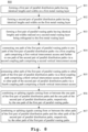
- a first pair of parallel distribution paths having identical lengths and widths is formed on a first metal routing layer.
- a second pair of parallel distribution paths having identical lengths and widths is formed on the first metal routing layer.
- a third step 803 a first pair of parallel routing paths having identical lengths and widths is formed on a second metal routing layer being orthogonal to the first metal routing layer.
- one path of the first pair of parallel routing paths is connected to one path of the first pair of parallel distribution paths via a first coupling path comprising a first vertical interconnect access and further to one path of the second pair of parallel distribution paths via a second coupling path comprising a second vertical interconnect access.
- a fifth step 805 other path of the first pair of parallel routing paths is connected to other path of the first pair of parallel distribution paths via a third coupling path comprising a third vertical interconnect access and further to other path of the second pair of parallel distribution paths via a fourth coupling path comprising a fourth vertical interconnect access.
- a sixth step 806 signals coming from or between the one path of the first pair of parallel distribution paths and the one path of the second pair of parallel distribution paths are combined or split, respectively, by the one path of the first pair of parallel routing paths.
- a seventh step 807 signals coming from or between the other path of the first pair of parallel distribution paths and the other path of the second pair of parallel distribution paths are combined or split, respectively, by the other path of the first pair of parallel routing paths.
Landscapes
- Design And Manufacture Of Integrated Circuits (AREA)
Abstract
A network (200) of this disclosure comprises a first pair of parallel distribution paths (2011, 2012) realized on a first metal routing layer, a second pair of parallel distribution paths (2021, 2022) realized on the first metal routing layer, and a first pair of parallel routing paths (2031, 2032) realized on a second metal routing layer being orthogonal to the first metal routing layer. In this regard, one path (2031) of the first pair of parallel routing paths is connected to one path (2011) of the first pair of parallel distribution paths via a first coupling path (2041) and further to one path (2021) of the second pair of parallel distribution paths via a second coupling path (2042) in order to combine or split signals coming from or between the one path (2011) of the first pair of parallel distribution paths and the one path (2021) of the second pair of parallel distribution paths, respectively.
Description
- The invention relates to differential signal distribution, especially to splitter or combiner networks for routing high frequency, for example Radio Frequency (RF),differential signals.
- The differential signal branching, from the central point of symmetry to multiple signal tapping networks, must be carefully laid out to maintain symmetry. Generally, the symmetrical distribution of wiring requires that the electrical length of the signal lines must always be identical in the two parts, i.e., the positive signal path and the negative signal path, of the differential path, and the capacitive coupling, e.g., to other lines or to the substrate, must be as similar as possible in the two parts of the differential path.
- For example, the document
US 2011/0032065 A1 discloses a symmetrical transformer for differential signaling. A disadvantage ofUS 2011/0032065 A1 is that a symmetrical distribution of wiring is not utilized for routing the differential signal to or from the symmetrical transformer, which may affect the signal integrity in terms of imbalance between positive and negative signals. - Accordingly, an object of the invention is to provide an apparatus and a method for improving the signal integrity in terms of imbalance between positive and negative signals lines of a differential signal line.
- The object is solved by the features of the first independent claim for the apparatus and by the features of the second independent claim for the method. The dependent claims contain further developments.
- According to a first aspect of the invention, an apparatus for differential signal routing is provided. The apparatus comprises a first network comprising a first pair of parallel distribution paths having substantially identical lengths and widths realized on a first metal routing layer, a second pair of parallel distribution paths having substantially identical lengths and widths realized on the first metal routing layer, and a first pair of parallel routing paths having substantially identical lengths and widths realized on a second metal routing layer being orthogonal to the first metal routing layer.
- In this regard, one path of the first pair of parallel routing paths is connected to one path of the first pair of parallel distribution paths via a first coupling path comprising a first vertical interconnect access and further to one path of the second pair of parallel distribution paths via a second coupling path comprising a second vertical interconnect access in order to combine or split signals coming from or between the one path of the first pair of parallel distribution paths and the one path of the second pair of parallel distribution paths, respectively.
- Furthermore, other path of the first pair of parallel routing paths is connected to other path of the first pair of parallel distribution paths via a third coupling path comprising a third vertical interconnect access and further to other path of the second pair of parallel distribution paths via a fourth coupling path comprising a fourth vertical interconnect access in order to combine or split signals coming from or between the other path of the first pair of parallel distribution paths and the other path of the second pair of parallel distribution paths, respectively.
- Moreover, at least the first coupling path and the third coupling path have substantially identical lengths and widths, and at least the second coupling path and the fourth coupling path have substantially identical lengths and widths. Advantageously, e.g., for splitting or for combining differential signals, an imbalance between the positive signal and the negative signal of the differential signal can be drastically reduced by utilizing extreme symmetry between the positive signal path and the negative signal path, thereby improving the signal integrity.
- Preferably, the first metal routing layer and the second metal routing layer correspond to back-end-of-line (BEOL) metallization structures. For example, the BEOL metallization structure may be a part of an integrated circuit, especially comprising semiconductor based wafers with planar layers. The integrated circuit may further comprise a front-end-of-line (FEOL) with active devices, such as transistors, and the BEOL for signal routing.
- For example, the first metal routing layer and the second metal routing layer may be adjacent metal layers or levels of the planar integrated circuit BEOL metallization structure. In this regard, each of the vertical interconnect accesses may provide a vertical electrically conductive connection between the first metal routing layer and the second metal routing layer, thereby electrically connecting the first metal routing layer to the second metal routing layer. The first metal routing layer and the second metal routing layer may not be adjacent metal layers or levels of the planar integrated circuit BEOL metallization structure. In this regard, each of the vertical interconnect accesses may provide a vertical electrically conductive connection between the first metal routing layer and the second metal routing layer covering more layers, this is achieved by super-VIA's as known to the skilled person in the art. The super-VIA thereby electrically connecting the first metal routing layer to the non adjacent second metal routing layer.
- The vertical interconnect accesses are vertically connecting the metal layer which are in a horizontal plane. So the vertical interconnect accesses are orthogonal and upward/downward oriented with respect to the metal layers.
- Preferably, each of the first coupling path and the third coupling path comprises a number of turns identical to each other. Additionally or alternatively, each of the second coupling path and the fourth coupling path comprises a number of turns identical to each other.
- Preferably, the first coupling path, the second coupling path, the third coupling path, and the fourth coupling path have substantially identical lengths and widths, and identical number of turns. Advantageously, for example, the symmetry between the positive signal path and the negative signal path for each of the first pair of parallel distribution paths and the second pair of parallel distribution paths can be maintained.
- Preferably, the first coupling path, the second coupling path, the third coupling path, and the fourth coupling path have identical number of 45 degrees turns. In other words, the number of turns for each of the coupling paths may be identical to each other. The number of turns may comprise one or more turns between 40 degrees and 50 degrees, preferably between 42 degrees and 48 degrees, more preferably between 44 degrees and 46 degrees, most preferably one or more 45 degrees turns.
- Preferably, the first coupling path, the second coupling path, the third coupling path, and the fourth coupling path have identical number of 90 degrees turns. In other words, the number of turns for each of the coupling paths may be identical to each other. The number of turns may comprise one or more turns between 85 degrees and 95 degrees, preferably between 87 degrees and 93 degrees, more preferably between 89 degrees and 91 degrees, most preferably one or more 90 degrees turns.
- Alternatively, the number of turns may comprise one or more 22.5 degrees turns or other polygon shapes.
- Preferably, the one path of the first pair of parallel routing paths and the first pair of parallel distribution paths overlap at their respective cross-sections. In addition, the other path of the first pair of parallel routing paths and the second pair of parallel distribution paths overlap at their respective cross-sections.
- In this regard, the one path of the first pair of parallel routing paths and the first pair of parallel distribution paths may overlap at their respective cross-sections such that both the positive signal path and the negative signal path may operate with similar amount of capacitive coupling between them, e.g., formed at their respective cross-sections.
- Similarly, the other path of the first pair of parallel routing paths and the second pair of parallel distribution paths may overlap at their respective cross-sections such that both the positive signal path and the negative signal path may operate with similar amount of capacitive coupling between them, e.g., formed at their respective cross-sections.
- Preferably, the apparatus further comprises at least one second network. The second network comprises a second pair of parallel routing paths having substantially identical lengths and widths realized on the second metal routing layer, and a pair of vertical interconnect accesses being symmetrically arranged on the first metal routing layer with respect to the lengths of the first pair of parallel distribution paths or the second pair of parallel distribution paths, wherein each vertical interconnect access of the pair of vertical interconnect accesses is arranged on a respective distribution path of the first pair of parallel distribution paths or the second pair of parallel distribution paths.
- In this regard, the second pair of parallel routing paths are respectively connected to the pair of vertical interconnect accesses via a pair of coupling paths having substantially identical lengths and widths realized on the second metal routing layer, the pair of coupling paths being symmetrically connected to the second pair of parallel routing paths with respect to the lengths of the second pair of parallel routing paths in order to couple in or out a differential signal to or from the first pair of parallel distribution paths or the second pair of parallel distribution paths, respectively.
- Advantageously, e.g., for coupling in or for coupling out the differential signal, an imbalance between the positive signal and the negative signal of a differential signal can be drastically reduced by utilizing extreme symmetry between the positive signal path and the negative signal path, thereby improving the signal integrity. The second network allows to make a 90 degrees turn in both of the differential signal paths.
- Preferably, the widths of the second pair of parallel routing paths and the widths of the pair of coupling paths are substantially identical to each other. Alternatively, the widths of the second pair of parallel routing paths and the widths of the pair of coupling paths are different from each other.
- Advantageously, for example, the different coupling paths can be formed in a flexible manner within the design rule, e.g., to meet a certain area constraint, whereby maintain the symmetry between the positive signal path and the negative signal path.
- Preferably, each path of the pair of coupling paths comprises a number of turns identical to each other, especially a number of 45 degrees turns. In other words, the number of turns for each of the coupling paths may be identical to each other. The number of turns may comprise one or more turns between 40 degrees and 50 degrees, preferably between 42 degrees and 48 degrees, more preferably between 44 degrees and 46 degrees, most preferably one or more 45 degrees turns.
- Preferably, each path of the pair of coupling paths comprises a number of turns identical to each other, especially a number of 90 degrees turns. In other words, the number of turns for each of the coupling paths may be identical to each other. The number of turns may comprise one or more turns between 85 degrees and 95 degrees, preferably between 87 degrees and 93 degrees, more preferably between 89 degrees and 91 degrees, most preferably one or more 90 degrees turns.
- Alternatively, the number of turns may comprise one or more 22.5 degrees turns or other polygon shapes.
- Preferably, the second pair of parallel routing paths and the first pair of parallel distribution paths or the second pair of parallel distribution paths overlap at their respective cross-sections.
- In this regard, the second pair of parallel routing paths and the first pair of parallel distribution paths, or the second pair of parallel routing paths and the second pair of parallel distribution paths, may overlap at their respective cross-sections such that both the positive signal path and the negative signal path may operate with similar amount of capacitive coupling, e.g., formed at their respective cross-sections.
- According to a second aspect of the invention, a method is provided for differential signal routing. The method comprises a step of forming a first pair of parallel distribution paths having substantially identical lengths and widths on a first metal routing layer. The method further comprises a step of forming a second pair of parallel distribution paths having substantially identical lengths and widths on the first metal routing layer. Moreover, the method comprises a step of forming a first pair of parallel routing paths having substantially identical lengths and widths realized on a second metal routing layer being orthogonal to the first metal routing layer.
- The method further comprises a step of connecting one path of the first pair of parallel routing paths to one path of the first pair of parallel distribution paths via a first coupling path comprising a first vertical interconnect access and further to one path of the second pair of parallel distribution paths via a second coupling path comprising a second vertical interconnect access.
- In addition, the method comprises a step of connecting other path of the first pair of parallel routing paths to other path of the first pair of parallel distribution paths via a third coupling path comprising a third vertical interconnect access and further to other path of the second pair of parallel distribution paths via a fourth coupling path comprising a fourth vertical interconnect access.
- Furthermore, the method comprises a step of combining or splitting signals coming from or between the one path of the first pair of parallel distribution paths and the one path of the second pair of parallel distribution paths, respectively, by the one path of the first pair of parallel routing paths.
- Moreover, the method comprises a step of combining or splitting signals coming from or between the other path of the first pair of parallel distribution paths and the other path of the second pair of parallel distribution paths, respectively, by the other path of the first pair of parallel routing paths.
- Preferably, the method further comprises a step of forming a second pair of parallel routing paths having substantially identical lengths and widths on the second metal routing layer.
- In addition, the method comprises a step of symmetrically arranging a pair of vertical interconnect accesses on the first metal routing layer with respect to the lengths of the first pair of parallel distribution paths or the second pair of parallel distribution paths such that each vertical interconnect access of the pair of vertical interconnect accesses is arranged on a respective distribution path of the first pair of parallel distribution paths or the second pair of parallel distribution paths.
- Furthermore, the method comprises a step of forming a pair of coupling paths having substantially identical lengths and widths on the second metal routing layer such that the pair of coupling paths being symmetrically connected to the second pair of parallel routing paths with respect to the lengths of the second pair of parallel routing paths. Moreover, the method comprises a step of respectively connecting the second pair of parallel routing paths to the pair of vertical interconnect accesses via the pair of coupling paths in order to couple in or out a differential signal to or from the first pair of parallel distribution paths or the second pair of parallel distribution paths, respectively.
- The term "substantially identical" can be understood as having an identical property between multiple entities. Alternatively, the term "substantially identical" can be understood as having a property with a difference less than 10%, preferably less than 5%, more preferably less than 2%, most preferably less than 1% between multiple entities.
- It is to be noted that the method according to the second aspect corresponds to the apparatus according to the first aspect and its implementation forms. Accordingly, the method of the second aspect may have corresponding implementation forms. Further, the method of the second aspect achieves the same advantages and effects as the apparatus of the first aspect and its respective implementation forms.
- Exemplary embodiments of the invention are now further explained with respect to the drawings by way of example only, and not for limitation. In the drawings:
- Fig. 1
- shows an exemplary embodiment of the apparatus;
- Fig. 2
- shows a first exemplary embodiment of the first network;
- Fig. 3
- shows a second exemplary embodiment of the first network
- Fig. 4
- shows an exemplary signal flow for the network of
Fig. 3 ; - Fig. 5
- shows a first exemplary embodiment of the second network;
- Fig. 6
- shows a second exemplary embodiment of the second network;
- Fig. 7
- shows an exemplary signal flow for the network of
Fig. 6 ; and - Fig. 8
- shows an exemplary embodiment of the method.
- Reference will now be made in detail to the embodiments of the present invention, examples of which are illustrated in the accompanying drawings. However, the following embodiments of the present invention may be variously modified and the range of the present invention is not limited by the following embodiments.
- In
Fig. 1 , an exemplary embodiment of theapparatus 100 according to the first aspect of the invention is illustrated. Theapparatus 100 may correspond to a signal splitter or a signal combiner for splitting or combining differential signals, respectively. - As the frequency of the signals in a signal distribution is increased, capacitive and inductive effect become more dominant. The capacitance and inductance of the signal paths as well as the coupling and parasitic versions of both may become more pronounced and even dominant. Mismatches in the above mentioned paths will lead to erroneous behavior of the circuits connected to the signal distribution network. To minimize common mode effects differential signal distribution is often used in high frequency applications, for example RF. The embodiments described below provide a solution for differential signal distribution to further minimize the impact of capacitive and inductive elements inherent to any signal distribution system.
- For instance, the
apparatus 100 may comprise acentral network apparatus 100 may further comprise twocorner networks corner networks - For example, the
central network corner splitters corner splitters - In
Fig. 2 , a first exemplary embodiment of thefirst network 200 according to the first aspect of the invention is illustrated. Thefirst network 200 may correspond to the central network ofFig. 1 . - For example, the
first network 200 may comprise a first pair of distribution paths comprising a first path 2011 and a second path 2012, e.g., one for the positive signal (p-path) and the other for the negative signal (n-path) of the differential signal. Preferably, the first path 2011 and the second path 2012 of the first pair of distribution paths may have identical lengths and widths. - In this regard, the length of each of the first path 2011 and the second path 2012 of the first pair of distribution paths may correspond to the length or horizontal distance between the central network and one of the corner networks of
Fig. 1 , e.g., between the respective signal tapping points, to achieve symmetry in the horizontal signal distribution. For instance, the first path 2011 and the second path 2012 of the first pair of distribution paths may be realized on a first (M1) metal routing layer. - For instance, the
first network 200 may comprise a second pair of distribution paths comprising a first path 2021 and a second path 2022, e.g., one for the positive signal (p-path) and the other for the negative signal (n-path) of the differential signal. Preferably, the first path 2021 and the second path 2022 of the second pair of distribution paths may have identical lengths and widths. - In this regard, the length of each of the first path 2021 and the second path 2022 of the second pair of distribution paths may correspond to the length or horizontal distance between the central network and one of the corner networks of
Fig. 1 , e.g., between the respective signal tapping points, to achieve symmetry in the horizontal signal distribution. For instance, the first path 2021 and the second path 2022 of the second pair of distribution paths may be realized on the M1 metal routing layer. - For example, the
first network 200 may comprise a pair of routing paths comprising a first path 2031 and a second path 2032, e.g., one for the positive signal (p-path) and the other for the negative signal (n-path) of the differential signal. Preferably, the first path 2031 and the second path 2032 of the pair of routing paths may have identical lengths and widths. For instance, the first path 2031 and the second path 2032 of the pair of routing paths may be realized on a second (M2) metal routing layer. - In this regard, the M2 metal routing direction of the M2 routing layer may be orthogonal to the M1 metal routing direction of the M1 routing layer. This orthogonality is in the horizontal plane in which the metal layers are formed in for example integrated circuits (IC), more particularly CMOS IC's. It should be noted that the coupling paths are not restricted to the orthogonal restriction of the routing direction. As the coupling paths may comprise turns of 22.5, 45 or 90 degrees. Further the coupling paths may also comprise polygon shapes of other and multiple angles forming curves or bends if the integration technology allow for that. Preferably, the M1 metal routing layer and the M2 metal routing layer may be adjacent metal routing layers. The first and second metal layers can be interchanged. The first and second metal layers may be layers with other metal layers in between the first and second metal layers. In these embodiments the vertical interconnect accesses are covering multiple metal layers to cover the distance between the first and the second layer, this is achieved by so called super-VIA's, which are known in the art. The VIA's or super-VIA's are vertical interconnect structures so are orthogonal to the plane of the metal layers in planar integration technologies for fabricating IC's.
- For instance, the first path 2031 of the pair of routing paths may be connected to the first path 2011 of the first pair of distribution paths via a first coupling path 2041. In this regard, a first vertical interconnect access (VIA) 2051 may be arranged on the first coupling path 2041 to vertically connect the M1 metal routing layer and the M2 metal routing layer, thereby interconnecting the first path 2031 of the pair of routing paths and the first path 2011 of the first pair of distribution paths.
- For example, the first coupling path 2041 may comprise four successive 45 degrees turns. However, the first coupling path 2041 may comprise more than or less than four 45 degrees turns. Alternatively, the first coupling path 2041 may comprise a number of successive 22.5 degrees turns. Alternatively, the first coupling path 2041 may be realized in any polygon shapes that can be achieved within the design rule.
- For instance, the first path 2031 of the pair of routing paths may be further connected to the first path 2021 of the second pair of distribution paths via a second coupling path 2042. In this regard, a second VIA 2052 may be arranged on the second coupling path 2042 to vertically connect the M1 metal routing layer and the M2 metal routing layer, thereby interconnecting the first path 2031 of the pair of routing paths and the first path 2021 of the second pair of distribution paths.
- For example, the second coupling path 2042 may comprise four successive 45 degrees turns. However, the second coupling path 2042 may comprise more than or less than four 45 degrees turns. Alternatively, the second coupling path 2042 may comprise a number of successive 22.5 degrees turns. Alternatively, the second coupling path 2042 may be realized in any polygon shapes that can be achieved within the design rule.
- In this regard, the first path 2031 of the pair of routing paths may combine or split signals coming from or between the first path 2011 of the first pair of distribution paths and the first path 2021 of the second pair of distribution paths, respectively.
- For instance, the second path 2032 of the pair of routing paths may be connected to the second path 2012 of the first pair of distribution paths via a third coupling path 2043. In this regard, a third VIA 2053 may be arranged on the third coupling path 2043 to vertically connect the M1 metal routing layer and the M2 metal routing layer, thereby interconnecting the second path 2032 of the pair of routing paths and the second path 2012 of the first pair of distribution paths.
- For example, the third coupling path 2043 may comprise four successive 45 degrees turns. However, the third coupling path 2043 may comprise more than or less than four 45 degrees turns. Alternatively, the third coupling path 2043 may comprise a number of successive 22.5 degrees turns.
- Alternatively, the third coupling path 2043 may be realized in any polygon shapes that can be achieved within the design rule.
- For instance, the second path 2032 of the pair of routing paths may be further connected to the second path 2022 of the second pair of distribution paths via a fourth coupling path 2044. In this regard, a fourth VIA 2054 may be arranged on the fourth coupling path 2044 to vertically connect the M1 metal routing layer and the M2 metal routing layer, thereby interconnecting the second path 2032 of the pair of routing paths and the second path 2022 of the second pair of distribution paths.
- For example, the fourth coupling path 2044 may comprise four successive 45 degrees turns. However, the fourth coupling path 2044 may comprise more than or less than four 45 degrees turns. Alternatively, the fourth coupling path 2044 may comprise a number of successive 22.5 degrees turns. Alternatively, the fourth coupling path 2044 may be realized in any polygon shapes.
- In this regard, the second path 2032 of the pair of routing paths may combine or split signals coming from or between the second path 2012 of the first pair of distribution paths and the second path 2022 of the second pair of distribution paths, respectively.
- Preferably, the first coupling path 2041 and the third coupling path 2043 may have identical lengths, identical widths, identical number of turns, and/or identical polygon shapes. Additionally, the second coupling path 2042 and the fourth coupling path 2044 may have identical lengths, identical widths, identical number of turns, and/or identical polygon shapes.
- More preferably, the first coupling path 2041, the second coupling path 2042, the third coupling path 2043, and the fourth coupling path 2044 may have identical lengths, identical widths, identical number of turns, and/or identical polygon shapes.
- For example, the first coupling path 2041 may comprise a first portion 2071 realized on the M2 metal layer being connected to the first path 2031 of the pair of routing paths. The first coupling path 2041 may further comprise a second portion 2072 realized on the M1 metal layer being connected to the first path 2011 of the first pair of distribution paths. In this regard, the first VIA 2051 may interconnect the first portion 2071 and the second portion 2072 of the first coupling path 2041.
- For instance, the second coupling path 2042 may be realized on the M2 metal layer being connected to the first path 2031 of the pair of routing paths, e.g., forming a common branching point for both the first coupling path 2041 and the second coupling path 2042 from the first path 2031 of the pair of routing paths. In this regard, the second VIA 2052 may interconnect the second coupling path 2042 and the first path 2021 of the second pair of distribution paths.
- For example, the third coupling path 2043 may comprise a first portion 2081 realized on the M2 metal layer being connected to the second path 2032 of the pair of routing paths. The third coupling path 2043 may further comprise a second portion 2082 realized on the M1 metal layer being connected to the second path 2012 of the first pair of distribution paths. In this regard, the third VIA 2053 may interconnect the first portion 2081 and the second portion 2082 of the third coupling path 2043.
- For instance, the fourth coupling path 2044 may be realized on the M2 metal layer being connected to the second path 2032 of the pair of routing paths, e.g., forming a common branching point for both the third coupling path 2043 and the fourth coupling path 2044 from the second path 2032 of the pair of routing paths. In this regard, the fourth VIA 2054 may interconnect the fourth coupling path 2044 and the second path 2022 of the second pair of distribution paths.
- Preferably, the common branching point on the first path 2031 of the pair of routing paths and the common branching point on the second path 2032 of the pair of routing paths may be realized in a symmetrical manner with respect to the lengths of the pair of routing paths, i.e., at a distance along the length of each path of the pair of routing paths that is equivalent or identical to each other.
- For example, the first path 2031 of the pair of routing paths and the first path 2011 of the first pair of distribution paths may overlap at a first cross-section 2061. In addition, the second path 2032 of the pair of routing paths and the first path 2021 of the second pair of distribution paths may overlap at a second cross-section 2062.
- Furthermore, the first path 2031 of the pair of routing paths and the second path 2012 of the first pair of distribution paths may overlap at a third cross-section 2063. Moreover, the second path 2032 of the pair of routing paths and the second path 2022 of the second pair of distribution paths may overlap at a fourth cross-section 2064.
- In this regard, at the first cross-section 2061, the first path 2031 of the pair of routing paths and the first path 2011 of the first pair of distribution paths may operate in-phase, which may result in the coupling capacitance between two in-phase signals. In addition, at the second cross-section 2062, the second path 2032 of the pair of routing paths and the first path 2021 of the second pair of distribution paths may operate in antiphase, which may result in the coupling capacitance between two antiphase signals.
- Furthermore, at the third cross-section 2063, the first path 2031 of the pair of routing paths and the second path 2012 of the first pair of distribution paths may operate in antiphase, which may result in the coupling capacitance between two antiphase signals. Moreover, at the fourth cross-section 2064, the second path 2032 of the pair of routing paths and the second path 2022 of the second pair of distribution paths may operate in-phase, which may result in the coupling capacitance between two in-phase signals.
- In other words, the differential signal path from the first path 2031 of the pair of routing paths to the first path 2011 of the first pair of distribution paths via the first coupling path 2041 and the differential signal path from the second path 2032 of the pair of routing paths to the second path 2012 of the first pair of distribution paths via the third coupling path 2043 may experience an equivalent electrical length, width, line inductance, and an equivalent amount of coupling capacitance.
- Analogously, the differential signal path from the first path 2031 of the pair of routing paths to the first path 2021 of the second pair of distribution paths via the second coupling path 2042 and the differential signal path from the second path 2032 of the pair of routing paths to the second path 2022 of the second pair of distribution paths via the fourth coupling path 2044 may experience an equivalent electrical length, width, line inductance, and an equivalent amount of coupling capacitance.
- Therefore, especially due to the extreme symmetry between the p-path and the n-path of the differential signal paths, equivalent electrical length, width, line inductance, and an equivalent amount of coupling capacitance can be achieved for the p-path and the n-path, thereby improving the signal integrity.
- In
Fig. 3 , a second exemplary embodiment of thefirst network 300 according to the first aspect of the invention is illustrated. Thefirst network 300 may correspond to the central network ofFig. 1 . Thefirst network 300 may differ from thefirst network 200 in that the first coupling path 3041, the second coupling path 3042, the third coupling path 3043, and the fourth coupling path 3044 may have a number of consecutive 90 degrees turns. - For example, the first coupling path 3041 may comprise a first portion 3071 realized on the M2 metal layer (shown as darker grayscale) by extending the first path 2031 of the pair of routing paths. The first coupling path 3041 may further comprise a second portion 3072 realized on the M1 metal layer (shown as lighter grayscale) being extended from the first path 2011 of the first pair of distribution paths. In this regard, the first VIA 2051 may interconnect the first portion 3071 and the second portion 3072 of the first coupling path 3041.
- For instance, the second coupling path 3042 may be realized on the M2 metal layer by extending the first path 2031 of the pair of routing paths, e.g., forming a common branching point for both the first coupling path 3041 and the second coupling path 3042 at the first VIA 2051. In this regard, the second VIA 2052 may interconnect the second coupling path 3042 and the first path 2021 of the second pair of distribution paths.
- For example, the third coupling path 3043 may comprise a first portion 3081 realized on the M2 metal layer by extending the second path 2032 of the pair of routing paths. The third coupling path 3043 may further comprise a second portion 3082 realized on the M1 metal layer being extended from the second path 2012 of the first pair of distribution paths. In this regard, the third VIA 2053 may interconnect the first portion 3081 and the second portion 3082 of the third coupling path 3043.
- For instance, the fourth coupling path 3044 may be realized on the M2 metal layer by extending the second path 2032 of the pair of routing paths, e.g., forming a common branching point for both the third coupling path 3043 and the fourth coupling path 3044 at the third VIA 2053. In this regard, the fourth VIA 4054 may interconnect the fourth coupling path 3044 and the second path 2022 of the second pair of distribution paths.
- Preferably, the first coupling path 3041 and the third coupling path 3043 may have identical lengths, identical widths, identical number of turns, and/or identical shapes. Additionally, the second coupling path 3042 and the fourth coupling path 3044 may have identical lengths, identical widths, identical number of turns, and/or identical shapes.
- More preferably, the first coupling path 3041, the second coupling path 3042, the third coupling path 3043, and the fourth coupling path 3044 may have identical lengths, identical widths, identical number of turns, and/or identical shapes.
- For example, the first portion 3071 and the second portion 3072 of the first coupling path 3041 may overlap at a first cross-section 3061. In addition, the second portion 3072 of the first coupling path 3041 and the fourth coupling path 3044 may overlap at a second cross-section 3062. Furthermore, the second coupling path 3042 and the second portion 3082 of the third coupling path 3043 may overlap at a third cross-section 3063. Moreover, the first portion 3081 of the third coupling path 3043 and the fourth coupling path 3044 may overlap at a fourth cross-section 3064.
- In this regard, at the first cross-section 3061, the crossed-over paths may operate in-phase, which may result in the coupling capacitance between two in-phase signals. In addition, at the second cross-section 3062, the crossed-over paths may operate in antiphase, which may result in the coupling capacitance between two antiphase signals.
- Furthermore, at the third cross-section 3063, the crossed-over paths may operate in antiphase, which may result in the coupling capacitance between two antiphase signals. Moreover, at the fourth cross-section 3064, the crossed-over paths may operate in-phase, which may result in the coupling capacitance between two in-phase signals.
- In other words, the differential signal path from the first path 2031 of the pair of routing paths to the first path 2011 of the first pair of distribution paths via the first coupling path 3041 and the differential signal path from the second path 2032 of the pair of routing paths to the second path 2012 of the first pair of distribution paths via the third coupling path 3043 may experience an equivalent electrical length, width, line inductance, and an equivalent amount of coupling capacitance.
- Analogously, the differential signal path from the first path 2031 of the pair of routing paths to the first path 2021 of the second pair of distribution paths via the second coupling path 3042 and the differential signal path from the second path 2032 of the pair of routing paths to the second path 2022 of the second pair of distribution paths via the fourth coupling path 3044 may experience an equivalent electrical length, width, line inductance, and an equivalent amount of coupling capacitance.
- In
Fig. 4 , an exemplary signal flow for thenetwork 300 is illustrated. In particular, a split operation of a differential signal Pin, Nin from the pair of routing paths 2031, 2032 to the first pair of distribution paths 2011, 2012 and the second pair of distribution path 2021, 2022 is illustrated. In this example, the p-path is shown in the darker grayscale and the n-path is shown in the lighter grayscale. - The positive signal Pin may be inputted from the first path 2031 of the pair of routing paths and may be split between the first path 2011 of the first pair of distribution paths and the first path 2021 of the second pair of distribution paths (shown as Pout). Similarly, the negative signal Nin may be inputted from the second path 2032 of the pair of routing paths and may be split between the second path 2012 of the first pair of distribution paths and the second path 2022 of the second pair of distribution paths (shown as Nout).
- It can be seen that the signal path Pin-Pout from the first path 2031 of the pair of routing paths to the first path 2011 of the first pair of distribution paths and the signal path Nin-Nout from the second path 2032 of the pair of routing paths to the second path 2012 of the first pair of distribution paths may experience an equivalent electrical length, width, line inductance, and an equivalent amount of coupling capacitance.
- Analogously, the signal path Pin-Pout from the first path 2031 of the pair of routing paths to the first path 2021 of the second pair of distribution paths and the signal path Nin-Nout from the second path 2032 of the pair of routing paths to the second path 2022 of the second pair of distribution paths may experience an equivalent electrical length, width, line inductance, and an equivalent amount of coupling capacitance.
- It will be clear for the skilled person that if in
fig 4 . the inputs and outputs are interchanged and the signal direction indicated by the arrows are in opposite direction then the signal splitter operation will change to a signal combiner. - In
Fig. 5 , a first exemplary embodiment of thesecond network 500 according to the first aspect of the invention is illustrated. Thesecond network 500 may correspond to the corner network ofFig. 1 . - For example, the
second network 500 may comprise a pair of distribution paths. The pair of distribution paths may correspond to the first pair of distribution paths 2011, 2012 or the second pair of distribution paths 2021, 2022 of thefirst network Fig. 2 to Fig. 4 . It is to be noted, in the following, only the first pair of distribution paths 2011, 2012 is considered, and the implementation is analogous for the second pair of distribution paths 2021, 2022. - As mentioned before, the pair of distribution paths may comprise the first path 2011 and the second path 2012, e.g., one for the positive signal (p-path) and the other for the negative signal (n-path) of the differential signal, which may have identical lengths and widths.
- In this regard, the length of each of the first path 2011 and the second path 2012 of the pair of distribution paths may correspond to the length or horizontal distance between the central network and one of the corner networks of
Fig. 1 , e.g., between the respective signal tapping points, to achieve symmetry in the horizontal signal distribution. - Furthermore, the first path 2011 and the second path 2012 of the pair of distribution paths may be realized on the M1 metal routing layer.
- For example, the
second network 500 may comprise a pair of routing paths comprising a first path 5021 and a second path 5022, e.g., one for the positive signal (p-path) and the other for the negative signal (n-path) of the differential signal. Preferably, the first path 5021 and the second path 5022 of the pair of routing paths may have identical lengths and widths. For instance, the first path 5021 and the second path 5022 of the pair of routing paths may be realized on the M2 metal routing layer. - As mentioned before, the signal routing direction of the signal paths in the M2 metal routing layer may be orthogonal to the signal routing direction of the signal paths in the M1 metal routing layer. Preferably, the M1 metal routing layer and the M2 metal routing layer may be adjacent metal routing layers.
- For instance, the first path 5021 of the pair of routing paths may be connected to the first path 2011 of the pair of distribution paths via a first coupling path 5041. The first coupling path 5041 may be realized on the M2 metal routing layer being connected to the first path 5021 of the pair of routing paths and further to the first path 2011 of the pair of distribution paths through a first VIA 5031.
- In this regard, the first VIA 5031 may be arranged on the first path 2011 of the pair of distribution paths to vertically connect the M1 metal routing layer and the M2 metal routing layer, thereby interconnecting the first coupling path 5041 and the first path 2011 of the pair of distribution paths.
- For example, the second path 5022 of the pair of routing paths may be connected to the second path 2012 of the pair of distribution paths via a second coupling path 5042. The second coupling path 5042 may be realized on the M2 metal routing layer being connected to the second path 5022 of the pair of routing paths and further to the second path 2012 of the pair of distribution paths through a second VIA 5032.
- In this regard, the second VIA 5032 may be arranged on the second path 2012 of the pair of distribution paths to vertically connect the M1 metal routing layer and the M2 metal routing layer, thereby interconnecting the second coupling path 5042 and the second path 2012 of the first of distribution paths.
- For example, the first path 5021 of the pair of routing paths may route a signal to or from the first path 2011 of the pair of distribution paths via the first coupling path 5041 and the second path 5022 of the pair of routing paths may route a signal to or from the second path 2012 of the pair of distribution paths via the second coupling path 5042.
- For example, the first coupling path 5041 and the second coupling path 5042 may be connected to the first path 5021 of the pair of routing paths and the second path 5022 of the pair of routing paths, respectively, at points symmetrical to each other, i.e., at a distance along the length of each path of the pair of routing paths that is equivalent or identical to each other.
- In addition, the first VIA 5031 and the second VIA 5032 may be arranged on the first path 2011 of the pair of distribution paths and the second path 2012 of the pair of distribution paths, respectively, at points symmetrical to each other, i.e., at a distance along the length of each path of the pair of distribution paths that is equivalent or identical to each other.
- For example, the first coupling path 5041 may comprise two successive 45 degrees turns. However, the first coupling path 5041 may comprise more than or less than two 45 degrees turns. Alternatively, the first coupling path 5041 may comprise a number of successive 22.5 degrees turns. Alternatively, the first coupling path 5041 may be realized in any polygon shapes that can be achieved within the design rule.
- In addition, the second coupling path 5042 may comprise two successive 45 degrees turns. However, the second coupling path 5042 may comprise more than or less than two 45 degrees turns. Alternatively, the second coupling path 5042 may comprise a number of successive 22.5 degrees turns. Alternatively, the second coupling path 5042 may be realized in any polygon shapes that can be achieved within the design rule.
- For example, the first coupling path 5041 and the first path 5021 of the pair of routing paths may have identical widths. In addition, the second coupling path 5042 and the second path 5022 of the pair of routing paths may have identical widths. Preferably, the first coupling path 5041 and the second coupling path 5042 may have identical lengths, widths, identical number of turns, and/or identical polygon shapes.
- For example, the first path 5021 of the pair of routing paths and the first path 2011 of the pair of distribution paths may overlap at a first cross-section 5051. In addition, the second path 5022 of the pair of routing paths and the first path 2011 of the pair of distribution paths may overlap at a second cross-section 5052.
- Furthermore, the first path 5021 of the pair of routing paths and the second path 2012 of the pair of distribution paths may overlap at a third cross-section 5053. Moreover, the second path 5022 of the pair of routing paths and the second path 2022 of the pair of distribution paths may overlap at a fourth cross-section 5054.
- In this regard, at the first cross-section 5051, the first path 5021 of the pair of routing paths and the first path 2011 of the pair of distribution paths may operate in-phase, which may result in the coupling capacitance between two in-phase signals. In addition, at the second cross-section 5052, the second path 5022 of the pair of routing paths and the first path 2011 of the pair of distribution paths may operate in antiphase, which may result in the coupling capacitance between two antiphase signals.
- Furthermore, at the third cross-section 5053, the first path 5021 of the pair of routing paths and the second path 2012 of the pair of distribution paths may operate in antiphase, which may result in the coupling capacitance between two antiphase signals. Moreover, at the fourth cross-section 5054, the second path 5022 of the pair of routing paths and the second path 2022 of the pair of distribution paths may operate in-phase, which may result in the coupling capacitance between two in-phase signals.
- In other words, the differential signal path from the first path 5021 of the pair of routing paths to the first path 2011 of the pair of distribution paths via the first coupling path 5041 and the differential signal path from the second path 5022 of the pair of routing paths to the second path 2012 of the pair of distribution paths via the second coupling path 5042 may experience an equivalent electrical length, width, line inductance, and an equivalent amount of coupling capacitance.
- Therefore, especially due to the extreme symmetry between the p-path and the n-path of the differential signal paths, equivalent electrical length, width, line inductance, and an equivalent amount of coupling capacitance can be achieved for the p-path and the n-path, thereby improving the signal integrity.
- In
Fig. 6 , a second exemplary embodiment of thesecond network 600 according to the first aspect of the invention is illustrated. Thesecond network 600 may correspond to the corner network ofFig. 1 . Thesecond network 600 may differ from thesecond network 500 in that the first coupling path 6041 and the second coupling path 6042 may have a number of consecutive 90 degrees turns. - For example, the first coupling path 6041 may comprise three successive 90 degrees turns. However, the first coupling path 6041 may comprise more than or less than three 90 degrees turns. In addition, the second coupling path 6042 may comprise three successive 90 degrees turns. However, the second coupling path 6042 may comprise more than or less than three 90 degrees turns.
- For example, the first coupling path 6041 may have a smaller width than the width of the first path 5021 of the pair of routing paths. In addition, the second coupling path 6042 may have a smaller width than the width of the second path 5022 of the pair of routing paths. However, the first coupling path 6041 and the second coupling path 6042 may have identical lengths, widths, identical number of turns, and/or identical polygon shapes with respect to each other.
- In
Fig. 7 , an exemplary signal flow for thenetwork 600 is illustrated. In particular, a routing operation of a differential signal Pin, Nin from the pair of distribution paths 2011, 2012 to the pair of routing paths 5021, 5022 is illustrated. In this example, the p-path is shown in the darker grayscale and the n-path is shown in the lighter grayscale. - The negative signal Nin may be inputted from the first path 2011 of the pair of distribution paths and may be routed (shown as Nout) to the first path 5021 of the pair of routing paths via the first coupling path 6041. Similarly, the positive signal Pin may be inputted from the second path 2012 of the pair of distribution paths and may be routed (shown as Pout) to the second path 5022 of the pair of routing paths via the second coupling path 6042.
- It can be seen that the signal path Nin-Nout from the first path 2011 of the pair of distribution paths to the first path 5021 of the pair of routing paths and the signal path Pin-Pout from the second path 2012 of the pair of distribution paths to the second path 5022 of the pair of routing paths may experience an equivalent electrical length, width, line inductance, and an equivalent amount of coupling capacitance.
- In
Fig. 8 , an exemplary embodiment of themethod 800 according to the second aspect of the invention is illustrated. In afirst step 801, a first pair of parallel distribution paths having identical lengths and widths is formed on a first metal routing layer. In asecond step 802, a second pair of parallel distribution paths having identical lengths and widths is formed on the first metal routing layer. In athird step 803, a first pair of parallel routing paths having identical lengths and widths is formed on a second metal routing layer being orthogonal to the first metal routing layer. - In a
fourth step 804, one path of the first pair of parallel routing paths is connected to one path of the first pair of parallel distribution paths via a first coupling path comprising a first vertical interconnect access and further to one path of the second pair of parallel distribution paths via a second coupling path comprising a second vertical interconnect access. - In a
fifth step 805, other path of the first pair of parallel routing paths is connected to other path of the first pair of parallel distribution paths via a third coupling path comprising a third vertical interconnect access and further to other path of the second pair of parallel distribution paths via a fourth coupling path comprising a fourth vertical interconnect access. - In a
sixth step 806, signals coming from or between the one path of the first pair of parallel distribution paths and the one path of the second pair of parallel distribution paths are combined or split, respectively, by the one path of the first pair of parallel routing paths. In aseventh step 807, signals coming from or between the other path of the first pair of parallel distribution paths and the other path of the second pair of parallel distribution paths are combined or split, respectively, by the other path of the first pair of parallel routing paths. - It is important to note that, in the description as well as in the claims, the word "comprising" does not exclude other elements or steps and the indefinite article "a" or "an" does not exclude a plurality. A single element or other unit may fulfill the functions of several entities or items recited in the claims.
- It should be understood that the term "and/or" used in the specification and the appended claims of this application refers to any combination and all possible combinations of one or more associated listed items, and includes these combinations. It should also be understood that the word "connected" implies that the elements may be directly connected together or may be coupled through one or more intervening elements. Moreover, the disclosure with regard to any of the aspects is also relevant with regard to the other aspects of the disclosure.
- Although the invention has been illustrated and described with respect to one or more implementations, equivalent alterations and modifications will occur to others skilled in the art upon the reading and understanding of this specification and the annexed drawings. In addition, while a particular feature of the invention may have been disclosed with respect to only one of several implementations, such feature may be combined with one or more other features of the other implementations as may be desired and advantageous for any given or particular application.
Claims (15)
- An apparatus (100) for differential signal routing, the apparatus comprises a first network (200, 300) comprising:a first pair of parallel distribution paths (2011, 2012) having substantially identical lengths and widths realized on a first metal routing layer,a second pair of parallel distribution paths (2021, 2022) having substantially identical lengths and widths realized on the first metal routing layer, anda first pair of parallel routing paths (2031, 2032) having substantially identical lengths and widths realized on a second metal routing layer being orthogonal to the first metal routing layer,wherein one path (2031) of the first pair of parallel routing paths is connected to one path (2011) of the first pair of parallel distribution paths via a first coupling path (2041, 3041) comprising a first vertical interconnect access (2051) and further to one path (2021) of the second pair of parallel distribution paths via a second coupling path (2042, 3042) comprising a second vertical interconnect access (2052) in order to combine or split signals coming from or between the one path (2011) of the first pair of parallel distribution paths and the one path (2021) of the second pair of parallel distribution paths, respectively,
wherein other path (2032) of the first pair of parallel routing paths is connected to other path (2012) of the first pair of parallel distribution paths via a third coupling path (2043, 3043) comprising a third vertical interconnect access (2053) and further to other path (2022) of the second pair of parallel distribution paths via a fourth coupling path (2044, 3044) comprising a fourth vertical interconnect access (2054) in order to combine or split signals coming from or between the other path (2012) of the first pair of parallel distribution paths and the other path (2022) of the second pair of parallel distribution paths, respectively, wherein at least the first coupling path (2041, 3041) and the third coupling path (2043, 3043) have substantially identical lengths and widths, and at least the second coupling path (2042, 3042) and the fourth coupling path (2044, 3044) have substantially identical lengths and widths. - The apparatus according to claim 1,
wherein the first metal routing layer and the second metal routing layer correspond to back-end-of-line, BEOL, metallization structures. - The apparatus according to claim 1 or 2,wherein each of the first coupling path (2041, 3041) and the third coupling path (2043, 3043) comprises a number of turns identical to each other, and/orwherein each of the second coupling path (2042, 3042) and the fourth coupling path (2044, 3044) comprises a number of turns identical to each other.
- The apparatus according to any of claims 1 to 3, wherein the first coupling path (2041, 3041), the second coupling path (2042, 3042), the third coupling path (2043, 3043), and the fourth coupling path (2044, 3044) have substantially identical lengths, widths, and identical number of turns.
- The apparatus according to any of claims 1 to 4, wherein the first coupling path (2041, 3041), the second coupling path (2042, 3042), the third coupling path (2043, 3043), and the fourth coupling path (2044, 3044) have identical number of 45 degree turns.
- The apparatus according to any of claims 1 to 4, wherein the first coupling path (2041, 3041), the second coupling path (2042, 3042), the third coupling path (2043, 3043), and the fourth coupling path (2044, 3044) have identical number of 90 degree turns.
- The apparatus according to any of claims 1 to 6, wherein the one path (2031) of the first pair of parallel routing paths and the first pair of parallel distribution paths (2011, 2012) overlap at their respective cross-sections (2061, 2063), and
wherein the other path (2032) of the first pair of parallel routing paths and the second pair of parallel distribution paths (2021, 2022) overlap at their respective cross-sections (2062, 2064). - The apparatus according to any of claims 1 to 7, wherein the apparatus further comprises at least one second network (500, 600) comprising:a second pair of parallel routing paths (5021, 5022) having substantially identical lengths and widths realized on the second metal routing layer, anda pair of vertical interconnect accesses (5031, 5032) being symmetrically arranged on the first metal routing layer with respect to the lengths of the first pair of parallel distribution paths (2011, 2012) or the second pair of parallel distribution paths (2021, 2022), wherein each vertical interconnect access of the pair of vertical interconnect accesses (5031, 5032) is arranged on a respective distribution path of the first pair of parallel distribution paths (2011, 2012) or the second pair of parallel distribution paths (2021, 2022),wherein the second pair of parallel routing paths (5021, 5022) are respectively connected to the pair of vertical interconnect accesses (5031, 5032) via a pair of coupling paths (5041, 5042, 6041, 6042) having substantially identical lengths and widths realized on the second metal routing layer, the pair of coupling paths (5041, 5042, 6041, 6042) being symmetrically connected to the second pair of parallel routing paths (5021, 5022) with respect to the lengths of the second pair of parallel routing paths (5021, 5022) in order to couple in or out a differential signal to or from the first pair of parallel distribution paths (2011, 2012) or the second pair of parallel distribution paths (2021, 2022), respectively.
- The apparatus according to claim 8,
wherein the widths of the second pair of parallel routing paths (5021, 5022) and the widths of the pair of coupling paths (5041, 5042) are substantially identical to each other. - The apparatus according to claim 8,
wherein the widths of the second pair of parallel routing paths (5021, 5022) and the widths of the pair of coupling paths (6041, 6042) are different from each other. - The apparatus according to any of claims 8 to 10, wherein each path of the pair of coupling paths (5041, 5042, 6041, 6042) comprises a number of turns identical to each other, especially a number of 45 degree turns.
- The apparatus according to any of claims 8 to 10, wherein each path of the pair of coupling paths (5041, 5042, 6041, 6042) comprises a number of turns identical to each other, especially a number of 90 degree turns.
- The apparatus according to any of claims 8 to 12, wherein the second pair of parallel routing paths (5021, 5022) and the first pair of parallel distribution paths (2011, 2012) or the second pair of parallel distribution paths (2021, 2022) overlap at their respective cross-sections.
- A method (800) for differential signal routing comprising:forming (801) a first pair of parallel distribution paths having substantially identical lengths and widths on a first metal routing layer,forming (802) a second pair of parallel distribution paths having substantially identical lengths and widths on the first metal routing layer,forming (803) a first pair of parallel routing paths having substantially identical lengths and widths realized on a second metal routing layer being orthogonal to the first metal routing layer,connecting (804) one path of the first pair of parallel routing paths to one path of the first pair of parallel distribution paths via a first coupling path comprising a first vertical interconnect access and further to one path of the second pair of parallel distribution paths via a second coupling path comprising a second vertical interconnect access,connecting (805) other path of the first pair of parallel routing paths to other path of the first pair of parallel distribution paths via a third coupling path comprising a third vertical interconnect access and further to other path of the second pair of parallel distribution paths via a fourth coupling path comprising a fourth vertical interconnect access,combining or splitting (806) signals coming from or between the one path of the first pair of parallel distribution paths and the one path of the second pair of parallel distribution paths, respectively, by the one path of the first pair of parallel routing paths, andcombining or splitting (807) signals coming from or between the other path of the first pair of parallel distribution paths and the other path of the second pair of parallel distribution paths, respectively, by the other path of the first pair of parallel routing paths.
- The method according to claim 14,
wherein the method further comprises:forming a second pair of parallel routing paths having substantially identical lengths and widths on the second metal routing layer,symmetrically arranging a pair of vertical interconnect accesses on the first metal routing layer with respect to the lengths of the first pair of parallel distribution paths or the second pair of parallel distribution paths such that each vertical interconnect access of the pair of vertical interconnect accesses is arranged on a respective distribution path of the first pair of parallel distribution paths or the second pair of parallel distribution paths,forming a pair of coupling paths having substantially identical lengths and widths on the second metal routing layer such that the pair of coupling paths being symmetrically connected to the second pair of parallel routing paths with respect to the lengths of the second pair of parallel routing paths, andrespectively connecting the second pair of parallel routing paths to the pair of vertical interconnect accesses via the pair of coupling paths in order to couple in or out a differential signal to or from the first pair of parallel distribution paths or the second pair of parallel distribution paths, respectively.
Priority Applications (2)
| Application Number | Priority Date | Filing Date | Title |
|---|---|---|---|
| EP23219044.7A EP4576419A1 (en) | 2023-12-21 | 2023-12-21 | Apparatus and method for differential signal routing |
| US18/981,444 US20250210845A1 (en) | 2023-12-21 | 2024-12-13 | Apparatus and method for differential signal routing |
Applications Claiming Priority (1)
| Application Number | Priority Date | Filing Date | Title |
|---|---|---|---|
| EP23219044.7A EP4576419A1 (en) | 2023-12-21 | 2023-12-21 | Apparatus and method for differential signal routing |
Publications (1)
| Publication Number | Publication Date |
|---|---|
| EP4576419A1 true EP4576419A1 (en) | 2025-06-25 |
Family
ID=89308450
Family Applications (1)
| Application Number | Title | Priority Date | Filing Date |
|---|---|---|---|
| EP23219044.7A Pending EP4576419A1 (en) | 2023-12-21 | 2023-12-21 | Apparatus and method for differential signal routing |
Country Status (2)
| Country | Link |
|---|---|
| US (1) | US20250210845A1 (en) |
| EP (1) | EP4576419A1 (en) |
Citations (2)
| Publication number | Priority date | Publication date | Assignee | Title |
|---|---|---|---|---|
| US20110032065A1 (en) | 2009-08-07 | 2011-02-10 | Imec | Two Layer Transformer |
| US8482364B2 (en) * | 2009-09-13 | 2013-07-09 | International Business Machines Corporation | Differential cross-coupled power combiner or divider |
-
2023
- 2023-12-21 EP EP23219044.7A patent/EP4576419A1/en active Pending
-
2024
- 2024-12-13 US US18/981,444 patent/US20250210845A1/en active Pending
Patent Citations (2)
| Publication number | Priority date | Publication date | Assignee | Title |
|---|---|---|---|---|
| US20110032065A1 (en) | 2009-08-07 | 2011-02-10 | Imec | Two Layer Transformer |
| US8482364B2 (en) * | 2009-09-13 | 2013-07-09 | International Business Machines Corporation | Differential cross-coupled power combiner or divider |
Non-Patent Citations (1)
| Title |
|---|
| GRZYB J ET AL: "A wideband 240 GHz lens-integrated circularly polarized on-chip annular slot antenna for a FMCW radar transceiver module in SiGe technology", 2015 SBMO/IEEE MTT-S INTERNATIONAL MICROWAVE AND OPTOELECTRONICS CONFERENCE (IMOC), IEEE, 3 November 2015 (2015-11-03), pages 1 - 4, XP032840362, DOI: 10.1109/IMOC.2015.7369165 * |
Also Published As
| Publication number | Publication date |
|---|---|
| US20250210845A1 (en) | 2025-06-26 |
Similar Documents
| Publication | Publication Date | Title |
|---|---|---|
| US9559053B2 (en) | Compact vertical inductors extending in vertical planes | |
| JP5442358B2 (en) | Semiconductor device | |
| JP6461437B2 (en) | Noise filter circuit | |
| JPH0196953A (en) | Wiring structure | |
| US20090066457A1 (en) | Electronic device having transformer | |
| US7768372B2 (en) | Inductance comprising turns on several metallization levels | |
| US6373772B2 (en) | Semiconductor integrated circuit device having fuses and fuse latch circuits | |
| US11367773B2 (en) | On-chip inductor structure | |
| US7969014B2 (en) | Power layout of integrated circuits and designing method thereof | |
| KR20120125669A (en) | Stacked dual inductor structure | |
| US20180359848A1 (en) | Printed circuit board for high-speed transmission | |
| US7312683B1 (en) | Symmetrical inductor | |
| US8013689B2 (en) | Integrated circuit inductor with transverse interfaces | |
| US20250210845A1 (en) | Apparatus and method for differential signal routing | |
| US6744130B1 (en) | Isolated stripline structure | |
| KR20040018261A (en) | Three-level balun and its manufacturing method | |
| US8217747B2 (en) | Planar inductor | |
| US8878627B2 (en) | Monolithic power splitter for differential signal | |
| US7091614B2 (en) | Integrated circuit design for routing an electrical connection | |
| GB2609680A (en) | Interconnection structures to improve signal integrity within stacked dies | |
| CN114300439A (en) | Balun integrated structure and products with the same | |
| US8946905B2 (en) | Via structure for integrated circuits | |
| US9536820B1 (en) | Power distribution network | |
| US10149378B2 (en) | Communication device | |
| US11545480B2 (en) | Integrated circuit with single level routing |
Legal Events
| Date | Code | Title | Description |
|---|---|---|---|
| PUAI | Public reference made under article 153(3) epc to a published international application that has entered the european phase |
Free format text: ORIGINAL CODE: 0009012 |
|
| STAA | Information on the status of an ep patent application or granted ep patent |
Free format text: STATUS: THE APPLICATION HAS BEEN PUBLISHED |
|
| AK | Designated contracting states |
Kind code of ref document: A1 Designated state(s): AL AT BE BG CH CY CZ DE DK EE ES FI FR GB GR HR HU IE IS IT LI LT LU LV MC ME MK MT NL NO PL PT RO RS SE SI SK SM TR |
|
| STAA | Information on the status of an ep patent application or granted ep patent |
Free format text: STATUS: REQUEST FOR EXAMINATION WAS MADE |
|
| 17P | Request for examination filed |
Effective date: 20251027 |