EP4575906A1 - Optical computation device, learning method for optical computation device, and manufacturing method for optical computation device - Google Patents
Optical computation device, learning method for optical computation device, and manufacturing method for optical computation device Download PDFInfo
- Publication number
- EP4575906A1 EP4575906A1 EP23854691.5A EP23854691A EP4575906A1 EP 4575906 A1 EP4575906 A1 EP 4575906A1 EP 23854691 A EP23854691 A EP 23854691A EP 4575906 A1 EP4575906 A1 EP 4575906A1
- Authority
- EP
- European Patent Office
- Prior art keywords
- intensity distribution
- optical
- correct
- signal light
- detected
- Prior art date
- Legal status (The legal status is an assumption and is not a legal conclusion. Google has not performed a legal analysis and makes no representation as to the accuracy of the status listed.)
- Pending
Links
Images



Classifications
-
- G—PHYSICS
- G02—OPTICS
- G02F—OPTICAL DEVICES OR ARRANGEMENTS FOR THE CONTROL OF LIGHT BY MODIFICATION OF THE OPTICAL PROPERTIES OF THE MEDIA OF THE ELEMENTS INVOLVED THEREIN; NON-LINEAR OPTICS; FREQUENCY-CHANGING OF LIGHT; OPTICAL LOGIC ELEMENTS; OPTICAL ANALOGUE/DIGITAL CONVERTERS
- G02F3/00—Optical logic elements; Optical bistable devices
-
- G—PHYSICS
- G06—COMPUTING OR CALCULATING; COUNTING
- G06N—COMPUTING ARRANGEMENTS BASED ON SPECIFIC COMPUTATIONAL MODELS
- G06N3/00—Computing arrangements based on biological models
- G06N3/02—Neural networks
- G06N3/06—Physical realisation, i.e. hardware implementation of neural networks, neurons or parts of neurons
- G06N3/067—Physical realisation, i.e. hardware implementation of neural networks, neurons or parts of neurons using optical means
-
- G—PHYSICS
- G02—OPTICS
- G02F—OPTICAL DEVICES OR ARRANGEMENTS FOR THE CONTROL OF LIGHT BY MODIFICATION OF THE OPTICAL PROPERTIES OF THE MEDIA OF THE ELEMENTS INVOLVED THEREIN; NON-LINEAR OPTICS; FREQUENCY-CHANGING OF LIGHT; OPTICAL LOGIC ELEMENTS; OPTICAL ANALOGUE/DIGITAL CONVERTERS
- G02F1/00—Devices or arrangements for the control of the intensity, colour, phase, polarisation or direction of light arriving from an independent light source, e.g. switching, gating or modulating; Non-linear optics
- G02F1/01—Devices or arrangements for the control of the intensity, colour, phase, polarisation or direction of light arriving from an independent light source, e.g. switching, gating or modulating; Non-linear optics for the control of the intensity, phase, polarisation or colour
- G02F1/09—Devices or arrangements for the control of the intensity, colour, phase, polarisation or direction of light arriving from an independent light source, e.g. switching, gating or modulating; Non-linear optics for the control of the intensity, phase, polarisation or colour based on magneto-optical elements, e.g. exhibiting Faraday effect
-
- G—PHYSICS
- G02—OPTICS
- G02F—OPTICAL DEVICES OR ARRANGEMENTS FOR THE CONTROL OF LIGHT BY MODIFICATION OF THE OPTICAL PROPERTIES OF THE MEDIA OF THE ELEMENTS INVOLVED THEREIN; NON-LINEAR OPTICS; FREQUENCY-CHANGING OF LIGHT; OPTICAL LOGIC ELEMENTS; OPTICAL ANALOGUE/DIGITAL CONVERTERS
- G02F1/00—Devices or arrangements for the control of the intensity, colour, phase, polarisation or direction of light arriving from an independent light source, e.g. switching, gating or modulating; Non-linear optics
- G02F1/01—Devices or arrangements for the control of the intensity, colour, phase, polarisation or direction of light arriving from an independent light source, e.g. switching, gating or modulating; Non-linear optics for the control of the intensity, phase, polarisation or colour
- G02F1/13—Devices or arrangements for the control of the intensity, colour, phase, polarisation or direction of light arriving from an independent light source, e.g. switching, gating or modulating; Non-linear optics for the control of the intensity, phase, polarisation or colour based on liquid crystals, e.g. single liquid crystal display cells
-
- G—PHYSICS
- G06—COMPUTING OR CALCULATING; COUNTING
- G06E—OPTICAL COMPUTING DEVICES
- G06E3/00—Devices not provided for in group G06E1/00, e.g. for processing analogue or hybrid data
-
- G—PHYSICS
- G06—COMPUTING OR CALCULATING; COUNTING
- G06N—COMPUTING ARRANGEMENTS BASED ON SPECIFIC COMPUTATIONAL MODELS
- G06N3/00—Computing arrangements based on biological models
- G06N3/02—Neural networks
- G06N3/06—Physical realisation, i.e. hardware implementation of neural networks, neurons or parts of neurons
- G06N3/067—Physical realisation, i.e. hardware implementation of neural networks, neurons or parts of neurons using optical means
- G06N3/0675—Physical realisation, i.e. hardware implementation of neural networks, neurons or parts of neurons using optical means using electro-optical, acousto-optical or opto-electronic means
-
- G—PHYSICS
- G06—COMPUTING OR CALCULATING; COUNTING
- G06N—COMPUTING ARRANGEMENTS BASED ON SPECIFIC COMPUTATIONAL MODELS
- G06N3/00—Computing arrangements based on biological models
- G06N3/02—Neural networks
- G06N3/08—Learning methods
- G06N3/09—Supervised learning
Definitions
- optical modulation element which includes a plurality of cells and which is designed to optically execute given computation by causing beams of signal light having passed through the respective cells to interfere with each other.
- the optical computation involving use of such an optical modulation element is advantageous in terms of that this can be carried out at higher speed and with lower power consumption as compared to electronic computation involving use of a processor. Further, by causing a plurality of optical modulation elements to sequentially act on signal light, it is possible to easily realize high-level optical computation which cannot be realized with a single optical modulation element.
- Patent Literature 1 discloses an optical computation device which is called Diffractive Deep Neural Network (D 2 NN), constituted with use of an optical modulation element such as those described above.
- D 2 NN Diffractive Deep Neural Network
- An aspect of the present invention was made in view of the above problem, and has an object to provide an optical computation device having high class determination capability.
- a learning method in accordance with an aspect of the present invention is a learning method for training an optical computation device, the optical computation device including: an optical computation section which includes an optical modulation element including a plurality of cells having phase modulation amounts which have been set independently of each other or phase modulation amounts which are settable independently of each other; an optical detection section which detects an intensity distribution of signal light output from the optical computation section; and an estimation section which refers to a plurality of correct intensity distributions corresponding to a respective plurality of classes and estimates, on a basis of the intensity distribution detected by the optical detection section, a class to which information represented by an intensity distribution of signal light input into the optical computation section belongs, the learning method including: setting the plurality of correct intensity distributions so that a correct intensity distribution having a highest similarity to the intensity distribution detected by the optical detection section serves as a correct intensity distribution corresponding to a class to which the information represented by the intensity distribution of the signal light input into the optical computation section belongs.
- An optical computation device in accordance with an aspect of the present invention is an optical computation device including: an optical computation section which includes an optical modulation element including a plurality of cells having phase modulation amounts which have been set independently of each other or phase modulation amounts which are settable independently of each other; an optical detection section which detects an intensity distribution of signal light output from the optical computation section; and an estimation section which refers to a plurality of correct intensity distributions corresponding to a respective plurality of classes and estimates, on a basis of the intensity distribution detected by the optical detection section, a class to which information represented by an intensity distribution of signal light input into the optical computation section belongs, the plurality of correct intensity distributions being set so that a correct intensity distribution having a highest similarity to the intensity distribution detected by the optical detection section serves as a correct intensity distribution corresponding to a class to which the information represented by the intensity distribution of the signal light input into the optical computation section belongs.
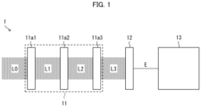
- Fig. 1 shows a side view illustrating a configuration of the optical computation device 1.
- the optical computation device 1 includes an optical computation section 11, an optical detection section 12, and an estimation section 13.
- the optical modulation elements 11a1 to 11an are arranged in such a manner that an exit surface of an optical modulation element 11ai' (i' is a natural number of not less than 1 and not more than n-1) and an entrance surface of an optical modulation element 11ai'+1 face each other.
- optical modulation elements 11a1 to 11an may be integrated together.
- n optical diffraction layers formed in a structure e.g., a dry gel which allows signal light to pass therethrough may be used as the optical modulation elements 11a1 to 11an.
- a configuration example of the optical modulation elements 11a1 to 11an will be described later with reference to a different drawing.
- Each optical modulation element 11ai (i is a natural number of not less than 1 and not more than n) is constituted by a plurality of cells having phase modulation amounts which have been set independently of each other or phase modulation amounts which are settable independently of each other.
- Each optical modulation element 11ai is a transmissive optical modulation element, and is configured to carry out optical computation by causing beams of transmission light subjected to phase modulation by the respective cells to interfere with each other.
- carrying out the optical computation means carrying out conversion of a two-dimensional intensity distribution of signal light by converting a two-dimensional intensity distribution indicative of information before computation into a two-dimensional intensity distribution indicative of information after the computation.
- the optical modulation element 11a1 carries out optical computation with respect to signal light L0 input into the optical computation section 11.
- An intensity distribution I of signal light L0 (hereinafter, such an intensity distribution may sometimes be referred to as an "input intensity distribution") represents information (e.g., an image) belonging to any one of a predetermined plurality of classes c1, c2, ... , cm (m is any natural number of not less than 2).
- Signal light Li' output from the optical modulation element 11ai' is input into the optical modulation element 11ai'+1.
- the optical modulation element 11ai'+1 carries out optical computation with respect to the signal light Li' output from the optical modulation element 11ai', that is, the signal light Li' indicative of a result of the optical computation carried out by the optical modulation element 11ai'.
- the present embodiment employs a configuration in which signal light L0 having been modulated by input information is input into the optical computation device 1.
- the present invention is not limited to this.
- Such a configuration can be realized by, for example, a configuration in which an optical modulation element which generates signal light L0 by modulating the carrier light with the input information is added to a location preceding to the optical computation section 11.
- the optical modulation element to be added may be integrated with the optical modulation elements 11a1 to 11an, which constitute the optical computation section 11.
- the optical computation device 1 may be provided with a control section which sets a phase modulation amount of each of the cells of the optical modulation element 11ai. This makes it possible to freely change content of optical computation to be executed by the optical computation device 1.
- the gel is preferably a gel which shrinks while keeping a similar shape when subjected to dehydration shrinkage; for example, the gel is preferably a gel used in the Implosion Fabrication process.
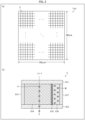
- Fig. 2 a configuration example of the optical modulation element 11ai included in the optical computation device 1.
- (a) of Fig. 2 is a plan view of an optical modulation element 11ai in accordance with the present specific example.
- (b) of Fig. 2 is a cross-sectional view of a cell C constituting the optical modulation element 11ai in accordance with the present specific example.
- the optical modulation element 11ai is constituted by a plurality of cells C having phase modulation amounts which are settable independently of each other.
- signal light Li-1 enters the optical modulation element 11ai, beams of the signal light Li-1 having passed through the cells C interfere with each other while being subjected to phase modulation, so that signal light Li indicative of a calculation result is formed.
- Each of the cells C constituting the optical modulation element 11ai is a microcell.
- the "microcell” herein refers to a cell having a cell size of less than 10 ⁇ m. Further, the "cell size” refers to a square root of an area of a cell. For example, in a case where the microcell has a square shape in a plan view, the cell size of the microcell refers to a length of a side of the microcell. A lower limit of the cell size of the microcell is 1 nm, for example.
- the optical modulation element 11ai shown in (a) of Fig. 2 is constituted by 200 ⁇ 200 cells C arranged in a matrix. Each of the cells C has a square shape of 500 nm ⁇ 500 nm in a plan view, and the optical modulation element 11ai has a square shape of 100 ⁇ m ⁇ 100 ⁇ m in a plan view.
- each of the cells C constituting the optical modulation element 11ai can be constituted by a polarizing plate C11, a polarizing plate C12, a first electrode C13, a magnetization free layer C14, an insulating layer C15, a magnetization fixed layer C16, and a second electrode C17.
- the polarizing plate C11 and the polarizing plate C12 are arranged so as to face each other.
- the first electrode C13, the magnetization free layer C14, the insulating layer C15, the magnetization fixed layer C16, and the second electrode C17 are stacked in this order and are sandwiched between the polarizing plate C11 and the polarizing plate C12.
- a direction in which the first electrode C13, the magnetization free layer C14, the insulating layer C15, the magnetization fixed layer C16, and the second electrode C17 are stacked is orthogonal to a direction in which the polarizing plate C11 and the polarizing plate C12 are stacked.
- a first side surface of the magnetization free layer C14 is in surface contact with one main surface of the polarizing plate C11, and a second side surface of the magnetization free layer C14 which second side surface is opposed to the first side surface is in surface contact with one main surface of the polarizing plate C12.
- the signal light Li-1 (1) enters an inside of the magnetization free layer C 14 via the polarizing plate C11, (2) passes through the magnetization free layer C14, and (3) exits to an outside of the magnetization free layer C14 via the polarizing plate C12.
- the magnetization free layer C14 is made of, for example, a soft magnetic material (e.g., CoFeB) having electric conductivity and light transmissivity.
- the magnetization fixed layer C16 is made of, for example, a hard magnetic material (e.g., permalloy) having electric conductivity.
- Selected as each of the polarizing plate C11 and the polarizing plate C12 is a polarizing plate which selectively allows a polarization component having a polarization direction P being in parallel with a magnetization direction M of the magnetization fixed layer C16 to transmit therethrough.
- (b) of Fig. 2 shows, as an example, a case where the magnetization direction M and the polarization direction P are in parallel with both the main surface of the polarizing plate C11 and the main surface of the magnetization fixed layer C16.
- a phase-shift amount of the signal light Li-1 in the cell C is determined depending on a magnitude of magnetization in the magnetization free layer C14.
- the magnitude of the magnetization in the magnetization free layer C14 is determined depending on a magnitude of the spin current injected into the magnetization free layer C14.
- the magnitude of the spin current injected into the magnetization free layer C14 is determined depending on the electric potential difference provided between the first electrode C13 and the second electrode C17.
- the cell C may be configured in a similar manner to a cell of a liquid crystal display (LCD).
- the cell C is constituted by a first glass substrate C21a, a first transparent electrode C22a, a liquid crystal layer C23, a second transparent electrode C22b, and a second glass substrate C21b.
- the first glass substrate C21a, the first transparent electrode C22a, the liquid crystal layer C23, the second transparent electrode C22b, and the second glass substrate C21b are stacked in this order from a side from which the signal light Li-1 enters.
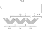
- Fig. 5 shows a side view illustrating a configuration of the optical computation device 2.
- the optical computation device 2 includes an optical computation section 21, an optical detection section 22, and an estimation section 23.
- Each optical modulation element 21ai (i is a natural number of not less than 1 and not more than n) is constituted by a plurality of cells having phase modulation amounts which have been set independently of each other or phase modulation amounts which are settable independently of each other.
- Each optical modulation element 21ai is a reflective optical modulation element.
- Each optical modulation element 21ai carries out optical computation by causing beams of reflected light having been subjected to phase modulation by the respective cells to interfere with each other.
- carrying out optical computation means carrying out conversion of two-dimensional intensity distribution of signal light by converting a two-dimensional intensity distribution indicative of information before computation into a two-dimensional intensity distribution indicative of information after the computation.
- the estimation section 23 is a means which refers to correct intensity distributions I"1, I"2, ... , I"m corresponding to a respective plurality of classes c1, c2, ... , cm so as to estimate, on the basis of a detected intensity distribution I', a class c ⁇ ⁇ c1, c2, ... , cm ⁇ to which information represented by the input intensity distribution I belongs.
- what is used as the estimation section 23 is a computer.
- the class c estimated by the estimation section 23 is displayed on a display connected to the estimation section 23, for example.
- the present embodiment employs a configuration in which signal light L0 having been modulated with input information is input into the optical computation device 2.
- the present invention is not limited to this.
- Such a configuration can be realized by, for example, a configuration in which an optical modulation element which generates signal light L0 by modulating carrier light with input information is added to a position preceding to the optical computation section 21.
- the optical modulation element to be added may be integrated with the optical modulation elements 21a1 to 21an, which constitute the optical computation section 21.
- the optical computation device 2 may be provided with a control section which sets a phase modulation amount of each of the cells of the optical modulation element 21ai. This makes it possible to freely change content of optical computation to be executed by the optical computation device 2.
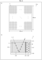
- Fig. 6 a configuration example of the optical modulation element 21ai included in the optical computation device 2.
- (a) of Fig. 6 is a plan view of an optical modulation element 21ai in accordance with the present specific example.
- (b) of Fig. 6 is a cross-sectional view of a cell C constituting the optical modulation element 21ai in accordance with the present specific example.
- the optical modulation element 21ai shown in (a) of Fig. 6 is constituted by 200 ⁇ 200 cells C arranged in a matrix. Each of the cells C has a square shape of 500 nm ⁇ 500 nm in a plan view, and the optical modulation element 21ai has a square shape of 100 ⁇ m ⁇ 100 ⁇ m in a plan view.
- the polarizing plate C11 and the reflection plate C18 are arranged so as to face each other.
- the first electrode C13, the magnetization free layer C14, the insulating layer C15, the magnetization fixed layer C16, and the second electrode C17 are stacked in this order and are sandwiched between the reflection plate C11 and the polarizing plate C18.
- a direction in which the first electrode C13, the magnetization free layer C14, the insulating layer C15, the magnetization fixed layer C16, and the second electrode C17 are stacked is orthogonal to a direction in which the polarizing plate C11 and the reflection plate C18 are stacked.
- the magnetization occurring in the magnetization free layer C14 is magnetization which is in parallel with the magnetization direction M of the magnetization fixed layer C16, that is, magnetization which is in parallel with the polarization direction P of the signal light Li-1 entering the magnetization free layer C14 through the polarizing plate C11. This causes a phase of the signal light Li-1 to be delayed by a transverse Kerr effect during a process of transmission in the magnetization free layer C14.
- the cell C can be configured in a similar manner to a cell of a liquid crystal on silicon (LCOS).
- the cell C is constituted by a glass substrate C21, a transparent electrode C22, a liquid crystal layer C23, and a reflective electrode C24.
- the glass substrate C21, the transparent electrode C22, the liquid crystal layer C23, and the reflective electrode C24 are stacked in this order from a side from which the signal light Li-1 enters.
- the liquid crystal layer C23 is constituted by liquid crystal molecules oriented in a direction which is in parallel with a main surface of the glass substrate C21, and has a refractive index corresponding to an electric potential difference between the transparent electrode C22 and the reflective electrode C24.
- the phase modulation amount of the cell C can be set at a desired value by regulating the electric potential difference provided between the transparent electrode C22 and the reflective electrode C24.
- the reflective optical modulation element 21ai can alternatively be constituted by a plurality of cells C which have thicknesses having been set independently of each other.
- Fig. 8 is an enlarged perspective view of a part of the optical modulation element 21ai constituted by the plurality of cells C which have thicknesses having been set independently of each other.
- the optical modulation element 21ai shown in Fig. 8 is constituted by a reflection plate C32 and a plurality of pillars formed on an upper surface of the reflection plate C32.
- Each of the pillars is structure that has a quadrangular prism shape and that has a square bottom surface having sides each having a length equal to that of a cell size, and functions as a cell C.
- a phase modulation amount of the signal light Li-1 reflected by each cell C is determined depending on a height of a pillar constituting the cell C. That is, signal light Li-1 reflected by a cell C constituted by a high pillar has a large phase modulation amount, and signal light reflected by a cell C constituted by a low pillar has a small phase modulation amount. Note that each of the cells C has a fixed phase modulation amount.
- the learning method M uses, as training data, p (p is a natural number of not less than 2) input intensity distributions I(1), I(2), ... , I(p) to optimize correct intensity distributions I"k corresponding to the respective classes ck. It is assumed here that a class ck(j) to which information represented by each input intensity distribution I(j) (j is a natural number of not less than 1 and not more than p) belongs is known and is usable as training data. In the following description, this class ck(j) ⁇ ⁇ c1, c2, ... , cm ⁇ will be referred to as a correct class corresponding to an input intensity distribution I(j), and a correct intensity distribution I"k(j) ⁇ ⁇ I" 1, I"2, ... , I"m ⁇ corresponding to this class ck(j) will be referred to as a correct intensity distribution corresponding to the input intensity distribution I(j).
- a phase modulation amount ⁇ i is expressed as a q-dimensional vector.
- a correct intensity distribution I"k is expressed as an r-dimensional vector. Since the number of optical modulation elements 11a1 to 11an is n and the number of classes Y1 to Ym is m, n q-dimensional vector(s) (i.e., n ⁇ q numerical value(s)) and m r-dimensional vectors (i.e., m ⁇ r numerical values) are set by the learning method M.
- each detected intensity distribution I'(j) represents an intensity distribution of signal light Ln detected by the optical detection section 12.
- each detected intensity distribution I'(j) is expressed as an r-dimensional vector, similarly to the correct intensity distribution I"k.
- the learning method M includes a derivation process M1 and an updating process M2. By executing these processes repeatedly, values of phase modulation amounts ⁇ 1, ⁇ 2, ... , ⁇ n and values of correct intensity distributions I"1, I"2, ... , I"m are sequentially optimized.
- the optimization herein means minimization of a loss function L (described later). It is assumed here that, before start of execution of the learning method M, the phase modulation amounts ⁇ 1, ⁇ 2, ... , ⁇ n and the correct intensity distributions I"1, I"2, ... , I”m are set at appropriate initial values (e.g., random initial values).
- the derivation process M1 is a process for deriving detected intensity distributions I'(1), I'(2), ... , I'(p).
- the processor derives, for each input intensity distribution I(j), a detected intensity distribution I'(j), which is an intensity distribution of signal light Ln detected by the optical detection section 12 in a case where an intensity distribution of signal light L0 input into the optical computation section 11 is an input intensity I(j).
- an initial value is used as a phase modulation amount ⁇ i of each cell constituting each optical modulation element 11ai.
- a value having been set in an updating process M2 for the previous epoch is used as a phase modulation amount ⁇ i of each cell constituting each optical modulation element 11ai.
- the updating process M2 is a process for setting (a) values of the phase modulation amounts ⁇ 1, ⁇ 2, ... , ⁇ n and (b) values of the correct intensity distributions I" 1, I"2, ... , I"m.
- what is used as the loss function L is a differentiable function of the phase modulation amounts ⁇ 1, ⁇ 2, ... , ⁇ n and the correct intensity distributions I"1, I"2, ... , I"m, the differentiable function satisfying the later-described conditions A and B with respect to the correct intensity distributions I"1, I"2, ... , I”m.
- the processor updates the values of the phase modulation amounts ⁇ 1, ⁇ 2, ... , ⁇ n and the values of the correct intensity distributions I"1, I"2, ... , I"m so that the loss function L takes a smaller value than a current value.
- the inventors of the present invention carried out optimization by use of the loss function L in accordance with the present specific example.
- a second specific example of the loss function L can be a loss function of ArcFace type.
- the ArcFace-type loss function L can be defined as below, for example.
- a third specific example of the loss function L can be a loss function of SphereFace type.
- the SphereFace-type loss function L can be defined as below, for example.
- a fourth specific example of the loss function L can be a loss function of CosFace type.
- the CosFace-type loss function L can be defined as below, for example.
- the scaling parameter s and the margin parameter ⁇ are optimized as hyper parameters.
- the phase modulation amounts ⁇ 1, ⁇ 2, ... , ⁇ n are implicitly included in the loss function L via I'(j), i.e., via ⁇ k,j .
- the above-described loss function L satisfies the conditions A and B described above. Therefore, setting the values of the correct intensity distributions I"1, I"2, ... , I"m by using the above-described loss function L enables the following. That is, by selecting, among the classes c1, c2, ... , cm, a class corresponding to a correct intensity distribution having a highest similarity to the detected intensity distribution I', it is possible to correctly estimate a class to which information represented by the input intensity distribution I belongs.
- the scaling parameter s and the margin parameters ⁇ 1, ⁇ 2, and ⁇ 3 are optimized as hyper parameters.
- the phase modulation amounts ⁇ 1, ⁇ 2, ... , ⁇ n are implicitly included in the loss function L via I'(j), i.e., via ⁇ k,j .
- a sixth specific example of the loss function L can be a loss function of a center loss type.
- the center-loss-type loss function L can be defined as below, for example.
- the above-described loss function L satisfies the conditions A and B described above. Therefore, setting the values of the correct intensity distributions I"1, I"2, ... , I"m by using the above-described loss function L enables the following. That is, by selecting, among the classes c1, c2, ... , cm, a class corresponding to a correct intensity distribution having a highest similarity to the detected intensity distribution I', it is possible to correctly estimate a class to which information represented by the input intensity distribution I belongs.
- a learning method in accordance with a first aspect of the present invention is a learning method for training an optical computation device, the optical computation device including: an optical computation section which includes an optical modulation element including a plurality of cells having phase modulation amounts which have been set independently of each other or phase modulation amounts which are settable independently of each other; an optical detection section which detects an intensity distribution of signal light output from the optical computation section; and an estimation section which refers to a plurality of correct intensity distributions corresponding to a respective plurality of classes and estimates, on a basis of the intensity distribution detected by the optical detection section, a class to which information represented by an intensity distribution of signal light input into the optical computation section belongs, the learning method including: setting the plurality of correct intensity distributions so that a correct intensity distribution having a highest similarity to the intensity distribution detected by the optical detection section serves as a correct intensity distribution corresponding to a class to which the information represented by the intensity distribution of the signal light input into the optical computation section belongs.
- an optical computation capability of the optical modulation element having been allocated to concentration of output signal light at a specific position which is a task not significant as information processing, can be used for class determination, which is a task significant as information processing.
- class determination which is a task significant as information processing.
- a learning method in accordance with a second aspect of the present invention is a learning method configured such that, in the learning method in accordance with the first aspect of the present invention, a plurality of input intensity distributions I(1), I(2), ... , I(p) (p is any natural number of not less than 2) and, among the plurality of classes c1, c2, ... , cm (m is any natural number of not less than 2), a class ck(j) to which information represented by each input intensity distribution I(j) (j is a natural number of not less than 1 and not more than p) belongs are used as training data; and the plurality of correct intensity distributions I"1, I"2, ...
- I"m are set by repeating (a) a derivation process and (b) an updating process, (a) the derivation process deriving, by use of an electromagnetic field simulation, a detected intensity distribution I'(j) which is an intensity distribution of signal light detected by the optical detection section in a case where the intensity distribution of the signal light input into the optical computation section is the input intensity distribution I(j), (b) the updating process updating the plurality of correct intensity distributions I"1, I"2, ... , I"m so that a loss function L takes a small value, (1) the loss function L taking a smaller value as a similarity between the detected intensity distribution I'(j) and, among the plurality of correct intensity distributions I"1, I"2, ...
- estimation of the class to which the information represented by the intensity distribution of the signal light input into the optical computation section belongs can be carried out with high precision on the basis of the Euclidean distance between the peak position (Xk(j),Yk(j)) of the correct intensity distribution I"k(j) and the peak position (X'(j),Y'(j)) of the detected intensity distribution I'(j).
- a learning method in accordance with a fourth aspect of the present invention is a learning method configured such that, in the learning method in accordance with the second aspect of the present invention, the similarity is an angle ⁇ k,j made by a correct intensity distribution I"k and the detected intensity distribution I'(j); and the loss function L is an ArcFace-type loss function, a SphereFace-type loss function, a CosFace-type loss function, or a loss function of a combination type, each of which is defined by using the angle ⁇ k,j .
- estimation of the class to which the information represented by the intensity distribution of the signal light input into the optical computation section belongs can be carried out with high precision on the basis of the angle ⁇ k,j made by the correct intensity distribution I"k and the detected intensity distribution I'(j).
- a learning method in accordance with a fifth aspect of the present invention is a learning method configured such that, in the learning method in accordance with the second aspect of the present invention, the similarity is an inner product I"k T I'(j) of a correct intensity distribution I"k and the detected intensity distribution I'(j); and the loss function L is a loss function of a center loss type defined by using the inner product I"k T I'(j).
- estimation of the class to which the information represented by the intensity distribution of the signal light input into the optical computation section belongs can be carried out with high precision on the basis of the inner product I"k' T I'(j) of the correct intensity distribution I"k and the detected intensity distribution I'(j).
- a learning method in accordance with a sixth aspect of the present invention is a manufacturing method for manufacturing an optical computation device, the optical computation device including: an optical computation section which includes an optical modulation element including a plurality of cells having phase modulation amounts which have been set independently of each other or phase modulation amounts which are settable independently of each other; an optical detection section which detects an intensity distribution of signal light output from the optical computation section; and an estimation section which refers to a plurality of correct intensity distributions corresponding to a respective plurality of classes and estimates, on a basis of the intensity distribution detected by the optical detection section, a class to which information represented by an intensity distribution of signal light input into the optical computation section belongs, the manufacturing method including: training the optical computation device by using a learning method recited in any one of the first to fifth aspects.
- an optical computation capability of the optical modulation element having been allocated to concentration of output signal light at a specific position which is a task not significant as information processing, can be used for class determination, which is a task significant as information processing.
- class determination which is a task significant as information processing.
- An optical computation device in accordance with a seventh aspect of the present invention is an optical computation device including: an optical computation section which includes an optical modulation element including a plurality of cells having phase modulation amounts which have been set independently of each other or phase modulation amounts which are settable independently of each other; an optical detection section which detects an intensity distribution of signal light output from the optical computation section; and an estimation section which refers to a plurality of correct intensity distributions corresponding to a respective plurality of classes and estimates, on a basis of the intensity distribution detected by the optical detection section, a class to which information represented by an intensity distribution of signal light input into the optical computation section, the plurality of correct intensity distributions being set so that a correct intensity distribution having a highest similarity to the intensity distribution detected by the optical detection section serves as a correct intensity distribution corresponding to a class to which the information represented by the intensity distribution of the signal light input into the optical computation section belongs.
- an optical computation capability of the optical modulation element having been allocated to concentration of output signal light at a specific position which is a task not significant as information processing, can be used for class determination, which is a task significant as information processing.
- class determination which is a task significant as information processing.
- An optical computation device in accordance with an eighth aspect of the present invention is an optical computation device configured such that, in the optical computation device in accordance with the seventh aspect of the present invention, the optical computation section includes a plurality of optical diffraction layers formed in a dry gel, each of the plurality of optical diffraction layers serving as the optical modulation element.
- the present invention is not limited to the foregoing embodiments, but can be modified by a person skilled in the art within the scope of the claims.
- the present invention also encompasses, in its technical scope, any embodiment derived by combining technical means disclosed in the foregoing embodiments.
Landscapes
- Physics & Mathematics (AREA)
- Engineering & Computer Science (AREA)
- Theoretical Computer Science (AREA)
- General Physics & Mathematics (AREA)
- Nonlinear Science (AREA)
- Biophysics (AREA)
- Life Sciences & Earth Sciences (AREA)
- Biomedical Technology (AREA)
- Health & Medical Sciences (AREA)
- Optics & Photonics (AREA)
- Data Mining & Analysis (AREA)
- Evolutionary Computation (AREA)
- Software Systems (AREA)
- Mathematical Physics (AREA)
- Artificial Intelligence (AREA)
- Computational Linguistics (AREA)
- General Engineering & Computer Science (AREA)
- Computing Systems (AREA)
- General Health & Medical Sciences (AREA)
- Molecular Biology (AREA)
- Neurology (AREA)
- Crystallography & Structural Chemistry (AREA)
- Power Engineering (AREA)
- Chemical & Material Sciences (AREA)
- Optical Modulation, Optical Deflection, Nonlinear Optics, Optical Demodulation, Optical Logic Elements (AREA)
- Image Analysis (AREA)
Abstract
Description
- The present invention relates to an optical computation device which carries out optical computation with use of an optical modulation element including a plurality of cells. The present invention further relates to a learning method and a manufacturing method for the optical computation device.
- There has been known an optical modulation element which includes a plurality of cells and which is designed to optically execute given computation by causing beams of signal light having passed through the respective cells to interfere with each other. The optical computation involving use of such an optical modulation element is advantageous in terms of that this can be carried out at higher speed and with lower power consumption as compared to electronic computation involving use of a processor. Further, by causing a plurality of optical modulation elements to sequentially act on signal light, it is possible to easily realize high-level optical computation which cannot be realized with a single optical modulation element.
-
Patent Literature 1 discloses an optical computation device which is called Diffractive Deep Neural Network (D2NN), constituted with use of an optical modulation element such as those described above. - [Patent Literature 1]
International Publication No.WO 2021/2327170 - In class determination involving use of the optical computation device disclosed in
Patent Literature 1, output signal light is concentrated at a position corresponding to a class to which information represented by input signal light belongs. This means that an optical computation capability of the optical modulation element is allocated not only to class determination, which is a task significant as information processing, but also to concentration of output signal light at a specific position, which is a task not significant as information processing. That is, the optical computation device disclosed inPatent Literature 1 has room for improvement of the class determination capability, in terms of that the optical computation capability of the optical modulation element having been allocated to a task not significant as information processing can be used for a task significant as information processing. - An aspect of the present invention was made in view of the above problem, and has an object to provide an optical computation device having high class determination capability. Solution to Problem
- A learning method in accordance with an aspect of the present invention is a learning method for training an optical computation device, the optical computation device including: an optical computation section which includes an optical modulation element including a plurality of cells having phase modulation amounts which have been set independently of each other or phase modulation amounts which are settable independently of each other; an optical detection section which detects an intensity distribution of signal light output from the optical computation section; and an estimation section which refers to a plurality of correct intensity distributions corresponding to a respective plurality of classes and estimates, on a basis of the intensity distribution detected by the optical detection section, a class to which information represented by an intensity distribution of signal light input into the optical computation section belongs, the learning method including: setting the plurality of correct intensity distributions so that a correct intensity distribution having a highest similarity to the intensity distribution detected by the optical detection section serves as a correct intensity distribution corresponding to a class to which the information represented by the intensity distribution of the signal light input into the optical computation section belongs.
- An optical computation device in accordance with an aspect of the present invention is an optical computation device including: an optical computation section which includes an optical modulation element including a plurality of cells having phase modulation amounts which have been set independently of each other or phase modulation amounts which are settable independently of each other; an optical detection section which detects an intensity distribution of signal light output from the optical computation section; and an estimation section which refers to a plurality of correct intensity distributions corresponding to a respective plurality of classes and estimates, on a basis of the intensity distribution detected by the optical detection section, a class to which information represented by an intensity distribution of signal light input into the optical computation section belongs, the plurality of correct intensity distributions being set so that a correct intensity distribution having a highest similarity to the intensity distribution detected by the optical detection section serves as a correct intensity distribution corresponding to a class to which the information represented by the intensity distribution of the signal light input into the optical computation section belongs. Advantageous Effects of Invention
- In accordance with an aspect of the present invention, it is possible to provide an optical computation device having high class determination capability.
-
-
Fig. 1 shows a side view illustrating a configuration of an optical computation device in accordance with a first embodiment of the present invention. -
Fig. 2 shows a plan view and a cross-sectional view illustrating a first configuration example of an optical modulation element included in the optical computation device shown inFig. 1 . -
Fig. 3 shows a cross-sectional view illustrating a second configuration example of an optical modulation element included in the optical computation device shown inFig. 1 . -
Fig. 4 shows a perspective view illustrating a third configuration example of an optical modulation element included in the optical computation device shown inFig. 1 . -
Fig. 5 shows a side view illustrating a configuration of an optical computation device in accordance with a second embodiment of the present invention. -
Fig. 6 shows a plan view and a cross-sectional view illustrating a first configuration example of an optical modulation element included in the optical computation device shown inFig. 5 . -
Fig. 7 shows a cross-sectional view illustrating a second configuration example of an optical modulation element included in the optical computation device shown inFig. 5 . -
Fig. 8 shows a perspective view illustrating a third configuration example of an optical modulation element included in the optical computation device shown inFig. 5 . -
Fig. 9 shows a flowchart illustrating a flow of a learning method in accordance with a third embodiment of the present invention. -
Fig. 10 illustrates an embodiment of the learning method shown inFig. 9 . (a) is a graph on which correct intensity distributions having been set in a second setting process for the first epoch are overlaid, and (b) is a graph on which correct intensity distributions having been set in a second setting process for the 322nd epoch are overlaid. - The following will describe, with reference to
Fig. 1 , a configuration of anoptical computation device 1 in accordance with a first embodiment of the present invention.Fig. 1 shows a side view illustrating a configuration of theoptical computation device 1. - As shown in
Fig. 1 , theoptical computation device 1 includes anoptical computation section 11, anoptical detection section 12, and anestimation section 13. - The
optical computation section 11 is constituted by at least one optical modulation element(s) 11a1 to 11an (n is any natural number of not less than 1; in the example shown inFig. 1 , n = 3). In the present embodiment, the optical modulation elements 11a1 to 11an are arranged in such a manner that an exit surface of an optical modulation element 11ai' (i' is a natural number of not less than 1 and not more than n-1) and an entrance surface of an opticalmodulation element 11ai'+ 1 face each other. - Note that the optical modulation elements 11a1 to 11an may be integrated together. For example, n optical diffraction layers formed in a structure (e.g., a dry gel) which allows signal light to pass therethrough may be used as the optical modulation elements 11a1 to 11an. A configuration example of the optical modulation elements 11a1 to 11an will be described later with reference to a different drawing.
- Each optical modulation element 11ai (i is a natural number of not less than 1 and not more than n) is constituted by a plurality of cells having phase modulation amounts which have been set independently of each other or phase modulation amounts which are settable independently of each other. Each optical modulation element 11ai is a transmissive optical modulation element, and is configured to carry out optical computation by causing beams of transmission light subjected to phase modulation by the respective cells to interfere with each other. Note here that carrying out the optical computation means carrying out conversion of a two-dimensional intensity distribution of signal light by converting a two-dimensional intensity distribution indicative of information before computation into a two-dimensional intensity distribution indicative of information after the computation.
- The optical modulation element 11a1 carries out optical computation with respect to signal light L0 input into the
optical computation section 11. An intensity distribution I of signal light L0 (hereinafter, such an intensity distribution may sometimes be referred to as an "input intensity distribution") represents information (e.g., an image) belonging to any one of a predetermined plurality of classes c1, c2, ... , cm (m is any natural number of not less than 2). Signal light Li' output from the optical modulation element 11ai' is input into the opticalmodulation element 11ai'+ 1. The opticalmodulation element 11ai'+ 1 carries out optical computation with respect to the signal light Li' output from the optical modulation element 11ai', that is, the signal light Li' indicative of a result of the optical computation carried out by the optical modulation element 11ai'. - The
optical detection section 12 is a means which detects signal light Ln output from theoptical computation section 11 and which generates an electric signal E indicative of an intensity distribution I' of the detected signal light Ln (hereinafter, such an intensity distribution may sometimes be referred to as a "detected intensity distribution"). In the present embodiment, what is used as theoptical detection section 12 is an image sensor constituted by photoelectric conversion cells (e.g., CCDs or CMOSs) arranged in a matrix. Note here that theoptical detection section 12 is not limited to the image sensor. For example, what is used as theoptical detection section 12 may be a sensor array constituted by a plurality of photoelectric conversion elements (e.g., photodiodes) arranged in predetermined positions. The electric signal E generated by theoptical detection section 12 is input into theestimation section 13. - The
estimation section 13 is a means which refers to correct intensity distributions I"1, I"2, ... , I"m corresponding to a respective plurality of classes c1, c2, ... , cm so as to estimate, on the basis of a detected intensity distribution I', a class c∈ {c1, c2, ... , cm} to which information represented by the input intensity distribution I belongs. In the present embodiment, what is used as theestimation section 13 is a computer. The class c estimated by theestimation section 13 is displayed on a display connected to theestimation section 13, for example. - The correct intensity distributions I" 1, I"2, ... , I"m which are referred to by the
estimation section 13 are set so that a correct intensity distribution having a highest similarity to the detected intensity distribution I' serves as a correct intensity distribution corresponding to the class c to which the information represented by the input intensity distribution I belongs. This configuration which selects, among the classes c1, c2, ... , cm, a class corresponding to a correct intensity distribution having a highest similarity to the detected intensity distribution I' enables correct estimation of a class to which information represented by the input intensity distribution I belongs. A learning method M for setting the correct intensity distributions I"1, I"2, ... I"m in the above-described manner will be described later with reference to a different drawing. - Note here that the present embodiment employs a configuration in which signal light L0 having been modulated by input information is input into the
optical computation device 1. However, the present invention is not limited to this. Alternatively, for example, it is possible to employ a configuration in which input information and carrier light are input into theoptical computation device 1. Such a configuration can be realized by, for example, a configuration in which an optical modulation element which generates signal light L0 by modulating the carrier light with the input information is added to a location preceding to theoptical computation section 11. In this case, the optical modulation element to be added may be integrated with the optical modulation elements 11a1 to 11an, which constitute theoptical computation section 11. - Further, in a case where each of the cells of the optical modulation element 11ai has a phase modulation amount which is variable, the
optical computation device 1 may be provided with a control section which sets a phase modulation amount of each of the cells of the optical modulation element 11ai. This makes it possible to freely change content of optical computation to be executed by theoptical computation device 1. - Further, in a case where n optical diffraction layers formed in a dry gel are used as the optical modulation elements 11a1 to 11an, the gel is preferably a gel which shrinks while keeping a similar shape when subjected to dehydration shrinkage; for example, the gel is preferably a gel used in the Implosion Fabrication process. With this, by drying a swollen gel in which n optical diffraction layers are formed, it is possible to easily manufacture an
optical computation section 11 in which the n optical diffraction layers are arranged with high precision. - The following will describe, with reference to
Fig. 2 , a configuration example of the optical modulation element 11ai included in theoptical computation device 1. (a) ofFig. 2 is a plan view of an optical modulation element 11ai in accordance with the present specific example. (b) ofFig. 2 is a cross-sectional view of a cell C constituting the optical modulation element 11ai in accordance with the present specific example. - As shown in (a) of
Fig. 2 , the optical modulation element 11ai is constituted by a plurality of cells C having phase modulation amounts which are settable independently of each other. When signal light Li-1 enters the optical modulation element 11ai, beams of the signal light Li-1 having passed through the cells C interfere with each other while being subjected to phase modulation, so that signal light Li indicative of a calculation result is formed. - Each of the cells C constituting the optical modulation element 11ai is a microcell. The "microcell" herein refers to a cell having a cell size of less than 10 µm. Further, the "cell size" refers to a square root of an area of a cell. For example, in a case where the microcell has a square shape in a plan view, the cell size of the microcell refers to a length of a side of the microcell. A lower limit of the cell size of the microcell is 1 nm, for example.
- The optical modulation element 11ai shown in (a) of
Fig. 2 is constituted by 200 × 200 cells C arranged in a matrix. Each of the cells C has a square shape of 500 nm × 500 nm in a plan view, and the optical modulation element 11ai has a square shape of 100 µm × 100 µm in a plan view. - For example, as shown in (b) of
Fig. 2 , each of the cells C constituting the optical modulation element 11ai can be constituted by a polarizing plate C11, a polarizing plate C12, a first electrode C13, a magnetization free layer C14, an insulating layer C15, a magnetization fixed layer C16, and a second electrode C17. - The polarizing plate C11 and the polarizing plate C12 are arranged so as to face each other. The first electrode C13, the magnetization free layer C14, the insulating layer C15, the magnetization fixed layer C16, and the second electrode C17 are stacked in this order and are sandwiched between the polarizing plate C11 and the polarizing plate C12. Here, a direction in which the first electrode C13, the magnetization free layer C14, the insulating layer C15, the magnetization fixed layer C16, and the second electrode C17 are stacked is orthogonal to a direction in which the polarizing plate C11 and the polarizing plate C12 are stacked. Thus, a first side surface of the magnetization free layer C14 is in surface contact with one main surface of the polarizing plate C11, and a second side surface of the magnetization free layer C14 which second side surface is opposed to the first side surface is in surface contact with one main surface of the polarizing plate C12. The signal light Li-1 (1) enters an inside of the magnetization free layer C 14 via the polarizing plate C11, (2) passes through the magnetization free layer C14, and (3) exits to an outside of the magnetization free layer C14 via the polarizing plate C12.
- The magnetization free layer C14 is made of, for example, a soft magnetic material (e.g., CoFeB) having electric conductivity and light transmissivity. The magnetization fixed layer C16 is made of, for example, a hard magnetic material (e.g., permalloy) having electric conductivity. Selected as each of the polarizing plate C11 and the polarizing plate C12 is a polarizing plate which selectively allows a polarization component having a polarization direction P being in parallel with a magnetization direction M of the magnetization fixed layer C16 to transmit therethrough. (b) of
Fig. 2 shows, as an example, a case where the magnetization direction M and the polarization direction P are in parallel with both the main surface of the polarizing plate C11 and the main surface of the magnetization fixed layer C16. - When an electric potential difference is provided between the first electrode C13 and the second electrode C17, a tunnel effect occurs and a spin current (a flow of spin-polarized electrons) is injected from the magnetization fixed layer C16 through the insulating layer C15 into the magnetization free layer C14 so as to magnetize the magnetization free layer C14. Here, the magnetization occurring in the magnetization free layer C14 is magnetization which is in parallel with the magnetization direction M of the magnetization fixed layer C16, that is, magnetization which is in parallel with the polarization direction P of the signal light Li-1 entering the magnetization free layer C14 through the polarizing plate C11. This causes a phase of the signal light Li-1 to be delayed by a transverse Kerr effect during a process of transmission in the magnetization free layer C14.
- Here, a phase-shift amount of the signal light Li-1 in the cell C is determined depending on a magnitude of magnetization in the magnetization free layer C14. The magnitude of the magnetization in the magnetization free layer C14 is determined depending on a magnitude of the spin current injected into the magnetization free layer C14. The magnitude of the spin current injected into the magnetization free layer C14 is determined depending on the electric potential difference provided between the first electrode C13 and the second electrode C17. Thus, regulating the electric potential difference provided between the first electrode C13 and the second electrode C17 can set the phase modulation amount of the cell C at a desired value.
- The description of the present configuration example has dealt with the cell C having a similar configuration to that of a magnetoresistive random access memory (MRAM) of spin transfer torque (STT) type. However, this is not limitative. For example, a cell C having a similar configuration to that of a MRAM of spin orbit torque (SOT) type may be used. Note that such a cell C can be realized by removing, from the structure indicated in (b) of
Fig. 2 , the insulating layer C15, the magnetization fixed layer C16, and the second electrode C17, for example. In this case, for example, it is possible to efficiently inject a spin flow into the magnetization free layer C14 by incorporating heavy metal into the first electrode C13 and giving a pulsed voltage or a pulsed current to the first electrode C13. - Further, the cell C may be configured in a similar manner to a cell of a liquid crystal display (LCD). In this case, for example, as shown in
Fig. 3 , the cell C is constituted by a first glass substrate C21a, a first transparent electrode C22a, a liquid crystal layer C23, a second transparent electrode C22b, and a second glass substrate C21b. The first glass substrate C21a, the first transparent electrode C22a, the liquid crystal layer C23, the second transparent electrode C22b, and the second glass substrate C21b are stacked in this order from a side from which the signal light Li-1 enters. - The signal light Li-1 (1) passes through the first glass substrate C21a and the first transparent electrode C22a, (2) passes through the liquid crystal layer C23, and (3) passes through the second transparent electrode C22b and the second glass substrate C21b. The liquid crystal layer C23 is constituted by liquid crystal molecules oriented in a direction which is parallel with a main surface of the glass substrate C21, and has a refractive index corresponding to an electric potential difference between the first transparent electrode C22a and the second transparent electrode C22b. Thus, the signal light Li-1 is subjected to phase modulation when passing through the liquid crystal layer C23. The phase modulation amount of the cell C can be set at a desired value by regulating the electric potential difference provided between the first transparent electrode C22a and the second transparent electrode C22b.
- Note that the optical modulation element 11ai can alternatively be constituted by a plurality of cells C which have thicknesses having been set independently of each other.
Fig. 4 is an enlarged perspective view of a part of the optical modulation element 11ai constituted by the plurality of cells C which have thicknesses having been set independently of each other. - The optical modulation element 11ai shown in
Fig. 4 is constituted by a transparent substrate C31 and a plurality of pillars formed on an upper surface of the transparent substrate C31. Each of the pillars is structure that has a quadrangular prism shape and that has a square bottom surface having sides each having a length equal to that of a cell size, and functions as a cell C. - The signal light Li-1 (1) enters the pillar through the upper surface, (2) passes through the pillar, (3) passes through the transparent substrate C31, and (4) is emitted from a lower surface of the transparent substrate C31. A phase modulation amount of the signal light Li-1 passing through each cell C is determined depending on a height of a pillar constituting the cell C. That is, signal light Li-1 passing through a cell C constituted by a high pillar has a large phase modulation amount, whereas signal light Li-1 passing through a cell C constituted by a low pillar has a small phase modulation amount. Note that each of the cells C has a fixed phase modulation amount.
- The following will describe, with reference to
Fig. 5 , a configuration of anoptical computation device 2 in accordance with a second embodiment of the present invention.Fig. 5 shows a side view illustrating a configuration of theoptical computation device 2. - As shown in
Fig. 5 , theoptical computation device 2 includes anoptical computation section 21, anoptical detection section 22, and anestimation section 23. - The
optical computation section 21 is constituted by at least one optical modulation element(s) 21a1 to 21an (n is any natural number of not less than 1; in the example shown inFig. 5 , n = 3) and amirror 21b. In the present embodiment, the optical modulation elements 21a1 to 21an are arranged such that their entrance/exit surfaces are included in a single plane. Themirror 21b is disposed so that its reflection surface faces the entrance/exit surfaces of the optical modulation elements 21a1 to 21an. - Note that the optical modulation elements 21a1 to 21an may be integrated together. For example, n optical diffraction layers formed in a structure (e.g., a dry gel) which allows signal light to pass therethrough may be used as the optical modulation elements 21a1 to 21an. Alternatively, the optical modulation elements 21a1 to 21an may be buried in a single substrate, or n areas of a single optical modulation substrate may be used as the optical modulation elements 21a1 to 21an. A configuration example of the optical modulation elements 21a1 to 21an will be described later with reference to a different drawing.
- Each optical modulation element 21ai (i is a natural number of not less than 1 and not more than n) is constituted by a plurality of cells having phase modulation amounts which have been set independently of each other or phase modulation amounts which are settable independently of each other. Each optical modulation element 21ai is a reflective optical modulation element. Each optical modulation element 21ai carries out optical computation by causing beams of reflected light having been subjected to phase modulation by the respective cells to interfere with each other. Note here that carrying out optical computation means carrying out conversion of two-dimensional intensity distribution of signal light by converting a two-dimensional intensity distribution indicative of information before computation into a two-dimensional intensity distribution indicative of information after the computation.
- The optical modulation element 21a1 carries out optical computation with respect to signal light L0 input into the
optical computation section 21. An intensity distribution I of signal light L0 (hereinafter, such an intensity distribution may sometimes be referred to as an "input intensity distribution") indicates information (e.g., an image) belonging to any one of a predetermined plurality of classes c1, c2, ... , cm (m is any natural number of not less than 2). Signal light Li' output from an optical modulation element 21ai' (i' is a natural number of not less than 1 and not more than n-1) is reflected by themirror 21b, and thereafter is input into an opticalmodulation element 21ai'+ 1. The optical modulation element 21ai'+1 carries out optical computation with respect to the signal light Li' output from the optical modulation element 21ai', that is, the signal light Li' indicative of a result of the optical computation carried out by the optical modulation element 21ai'. - The
optical detection section 22 is a means which detects signal light Ln output from theoptical computation section 21 and which generates an electric signal E indicative of an intensity distribution I' of the detected signal light Ln (hereinafter, such an intensity distribution may sometimes be referred to as a "detected intensity distribution"). In the present embodiment, what is used as theoptical detection section 22 is an image sensor constituted by photoelectric conversion cells (e.g., CCDs or CMOSs) arranged in a matrix. Note here that theoptical detection section 22 is not limited to the image sensor. For example, what is used as theoptical detection section 22 may be a sensor array constituted by a plurality of photoelectric conversion elements (e.g., photodiodes) arranged in predetermined positions. The electric signal E generated by theoptical detection section 22 is input into theestimation section 23. - The
estimation section 23 is a means which refers to correct intensity distributions I"1, I"2, ... , I"m corresponding to a respective plurality of classes c1, c2, ... , cm so as to estimate, on the basis of a detected intensity distribution I', a class c∈ {c1, c2, ... , cm} to which information represented by the input intensity distribution I belongs. In the present embodiment, what is used as theestimation section 23 is a computer. The class c estimated by theestimation section 23 is displayed on a display connected to theestimation section 23, for example. - The correct intensity distributions I" 1, I"2, ... , I"m which are referred to by the
estimation section 23 are set so that a correct intensity distribution having a highest similarity to the detected intensity distribution I' serves as a correct intensity distribution corresponding to the class c to which the information represented by the input intensity distribution I belongs. This configuration which selects, among the classes c1, c2, ... , cm, the class corresponding to the correct intensity distribution having a highest similarity to the detected intensity distribution I' enables correct estimation of the class to which the information represented by the input intensity distribution I belongs. A learning method M for setting the correct intensity distributions I"1, I"2, ... I"m in the above-described manner will be described later with reference to a different drawing. - Note here that the present embodiment employs a configuration in which signal light L0 having been modulated with input information is input into the
optical computation device 2. However, the present invention is not limited to this. Alternatively, for example, it is possible to employ a configuration in which input information and carrier light are input into theoptical computation device 2. Such a configuration can be realized by, for example, a configuration in which an optical modulation element which generates signal light L0 by modulating carrier light with input information is added to a position preceding to theoptical computation section 21. In this case, the optical modulation element to be added may be integrated with the optical modulation elements 21a1 to 21an, which constitute theoptical computation section 21. - Further, in a case where each of the cells of the optical modulation element 21ai has a phase modulation amount which is variable, the
optical computation device 2 may be provided with a control section which sets a phase modulation amount of each of the cells of the optical modulation element 21ai. This makes it possible to freely change content of optical computation to be executed by theoptical computation device 2. - Note that, in a case where n optical diffraction layers formed in a dry gel are used as the optical modulation elements 21a1 to 21an, the gel is preferably a gel which shrinks while keeping a similar shape when subjected to dehydration shrinkage; for example, the gel is preferably a gel used in the Implosion Fabrication process. With this, by drying a swollen gel in which n optical diffraction layers are formed, it is possible to easily manufacture an
optical computation section 21 in which the n optical diffraction layers are arranged with high precision. - The following will describe, with reference to
Fig. 6 , a configuration example of the optical modulation element 21ai included in theoptical computation device 2. (a) ofFig. 6 is a plan view of an optical modulation element 21ai in accordance with the present specific example. (b) ofFig. 6 is a cross-sectional view of a cell C constituting the optical modulation element 21ai in accordance with the present specific example. - As shown in (a) of
Fig. 6 , the optical modulation element 21ai is constituted by a plurality of cells C having phase modulation amounts which are settable independently of each other. When signal light Li-1 enters the optical modulation element 21ai, beams of the signal light Li-1 having been reflected by the cells C while being subjected to phase modulation interfere with each other, so that signal light Li indicative of a calculation result is formed. - Each of the cells C constituting the optical modulation element 21ai is a microcell. The "microcell" herein refers to a cell having a cell size of less than 10 µm. Further, the "cell size" refers to a square root of an area of a cell. For example, in a case where the microcell has a square shape in a plan view, the cell size of the microcell refers to a length of a side of the microcell. A lower limit of the cell size of the microcell is 1 nm, for example.
- The optical modulation element 21ai shown in (a) of
Fig. 6 is constituted by 200 × 200 cells C arranged in a matrix. Each of the cells C has a square shape of 500 nm × 500 nm in a plan view, and the optical modulation element 21ai has a square shape of 100 µm × 100 µm in a plan view. - For example, as shown in (b) of
Fig. 6 , each of the cells C constituting the optical modulation element 21ai can be constituted by a polarizing plate C11, a reflection plate C18, a first electrode C13, a magnetization free layer C14, an insulating layer C15, a magnetization fixed layer C16, and a second electrode C17. - The polarizing plate C11 and the reflection plate C18 are arranged so as to face each other. The first electrode C13, the magnetization free layer C14, the insulating layer C15, the magnetization fixed layer C16, and the second electrode C17 are stacked in this order and are sandwiched between the reflection plate C11 and the polarizing plate C18. Here, a direction in which the first electrode C13, the magnetization free layer C14, the insulating layer C15, the magnetization fixed layer C16, and the second electrode C17 are stacked is orthogonal to a direction in which the polarizing plate C11 and the reflection plate C18 are stacked. Thus, a first side surface of the magnetization free layer C14 is in surface contact with one main surface of the polarizing plate C11, and a second side surface of the magnetization free layer C14 which second side surface is opposed to the first side surface is in surface contact with one main surface of the reflection plate C18. The signal light Li-1 enters (1) an inside of the magnetization free layer C 14 via the polarizing plate C11, (2) is reflected by the reflection plate C18, and (3) exits to an outside of the magnetization free layer C14 via the polarizing plate C11.
- The magnetization free layer C14 is made of, for example, a soft magnetic material (e.g., CoFeB) having electric conductivity and light transmissivity. The magnetization fixed layer C16 is made of, for example, a hard magnetic material (e.g., permalloy) having electric conductivity. Selected as the polarizing plate C11 is a polarizing plate which selectively allows a polarization component having a polarization direction P which is in parallel with a magnetization direction M of the magnetization fixed layer C16 to transmit therethrough. (b) of
Fig. 6 shows, as an example, a case where the magnetization direction M and the polarization direction P are in parallel with both the main surface of the polarizing plate C11 and the main surface of the magnetization fixed layer C16. - When an electric potential difference is provided between the first electrode C13 and the second electrode C17, a tunnel effect occurs and a spin current (a flow of spin-polarized electrons) is injected from the magnetization fixed layer C16 through the insulating layer C15 into the magnetization free layer C14 so as to magnetize the magnetization free layer C14. Here, the magnetization occurring in the magnetization free layer C14 is magnetization which is in parallel with the magnetization direction M of the magnetization fixed layer C16, that is, magnetization which is in parallel with the polarization direction P of the signal light Li-1 entering the magnetization free layer C14 through the polarizing plate C11. This causes a phase of the signal light Li-1 to be delayed by a transverse Kerr effect during a process of transmission in the magnetization free layer C14.
- Here, a phase-shift amount of the signal light Li-1 in the cell C is determined depending on a magnitude of the magnetization in the magnetization free layer C14. The magnitude of the magnetization in the magnetization free layer C 14 is determined depending on a magnitude of the spin current injected into the magnetization free layer C14. The magnitude of the spin current injected into the magnetization free layer C14 is determined depending on the electric potential difference provided between the first electrode C13 and the second electrode C17. Thus, regulating the electric potential difference provided between the first electrode C13 and the second electrode C17 can set the phase modulation of the cell C at a desired value.
- The description of the present configuration example has dealt with the cell C having a similar configuration to that of a magnetoresistive random access memory (MRAM) of spin transfer torque (STT) type. However, this is not limitative. For example, a cell C having a similar configuration to that of a MRAM of spin orbit torque (SOT) type may be used. Note that such a cell C can be realized by removing, from the structure indicated in (b) of
Fig. 6 , the insulating layer C15, the magnetization fixed layer C16, and the second electrode C17, for example. In this case, for example, it is possible to efficiently inject a spin flow into the magnetization free layer C14 by incorporating heavy metal into the first electrode C13 and giving a pulsed voltage or a pulses current to the first electrode C13. - Further, the cell C can be configured in a similar manner to a cell of a liquid crystal on silicon (LCOS). In this case, for example, as shown in
Fig. 7 , the cell C is constituted by a glass substrate C21, a transparent electrode C22, a liquid crystal layer C23, and a reflective electrode C24. The glass substrate C21, the transparent electrode C22, the liquid crystal layer C23, and the reflective electrode C24 are stacked in this order from a side from which the signal light Li-1 enters. - The signal light Li-1 (1) passes through the glass substrate C21 and the transparent electrode C22, (2) passes through the liquid crystal layer C23, (3) is reflected by the reflective electrode C24, (4) passes through the liquid crystal layer C23, and (5) passes through the transparent electrode C22 and the glass substrate C21. The liquid crystal layer C23 is constituted by liquid crystal molecules oriented in a direction which is in parallel with a main surface of the glass substrate C21, and has a refractive index corresponding to an electric potential difference between the transparent electrode C22 and the reflective electrode C24. Thus, the signal light Li-1 is subjected to phase modulation when passing through the liquid crystal layer C23. The phase modulation amount of the cell C can be set at a desired value by regulating the electric potential difference provided between the transparent electrode C22 and the reflective electrode C24.
- The reflective optical modulation element 21ai can alternatively be constituted by a plurality of cells C which have thicknesses having been set independently of each other.
Fig. 8 is an enlarged perspective view of a part of the optical modulation element 21ai constituted by the plurality of cells C which have thicknesses having been set independently of each other. - The optical modulation element 21ai shown in
Fig. 8 is constituted by a reflection plate C32 and a plurality of pillars formed on an upper surface of the reflection plate C32. Each of the pillars is structure that has a quadrangular prism shape and that has a square bottom surface having sides each having a length equal to that of a cell size, and functions as a cell C. - The signal light Li-1 (1) enters the pillar through the upper surface, (2) passes through the pillar, (3) is reflected by the reflection plate C32, (4) passes through the pillar, and (5) is emitted from the upper surface of the pillar. A phase modulation amount of the signal light Li-1 reflected by each cell C is determined depending on a height of a pillar constituting the cell C. That is, signal light Li-1 reflected by a cell C constituted by a high pillar has a large phase modulation amount, and signal light reflected by a cell C constituted by a low pillar has a small phase modulation amount. Note that each of the cells C has a fixed phase modulation amount.
- The following will describe, with reference to
Fig. 9 , a flow of a learning method M in accordance with a third embodiment of the present invention.Fig. 9 shows a flowchart illustrating a flow of the learning method M. The following description will discuss the flow of the learning method M in accordance with the present embodiment which is applied to theoptical computation device 1 in accordance with the first embodiment. Note that the learning method M in accordance with the present embodiment is also applicable to theoptical computation device 2 in accordance with the second embodiment. The learning method M can be carried out by, for example, using a computer (e.g., theestimation section 13 included in theoptical computation device 1 or theestimation section 23 included in the optical computation device 2) including a processor and a memory. In this case, the processor carries out the learning method M by executing a program stored in the memory. - The learning method M uses, as training data, p (p is a natural number of not less than 2) input intensity distributions I(1), I(2), ... , I(p) to optimize correct intensity distributions I"k corresponding to the respective classes ck. It is assumed here that a class ck(j) to which information represented by each input intensity distribution I(j) (j is a natural number of not less than 1 and not more than p) belongs is known and is usable as training data. In the following description, this class ck(j) ∈ {c1, c2, ... , cm} will be referred to as a correct class corresponding to an input intensity distribution I(j), and a correct intensity distribution I"k(j) ∈ {I" 1, I"2, ... , I"m} corresponding to this class ck(j) will be referred to as a correct intensity distribution corresponding to the input intensity distribution I(j).
- In a case where the optical modulation element 11ai is constituted by q cells, a phase modulation amount Θi is expressed as a q-dimensional vector. Meanwhile, in a case where the
optical detection section 12 is constituted by r cells, a correct intensity distribution I"k is expressed as an r-dimensional vector. Since the number of optical modulation elements 11a1 to 11an is n and the number of classes Y1 to Ym is m, n q-dimensional vector(s) (i.e., n × q numerical value(s)) and m r-dimensional vectors (i.e., m × r numerical values) are set by the learning method M. - In the learning method M, p detected intensity distributions I'(1), I'(2), ... , I'(p) are used. In a case where an intensity distribution of signal light L0 input into the
optical computation section 11 is an input intensity distribution I(j), each detected intensity distribution I'(j) represents an intensity distribution of signal light Ln detected by theoptical detection section 12. In a case where theoptical detection section 12 is constituted by r cells, each detected intensity distribution I'(j) is expressed as an r-dimensional vector, similarly to the correct intensity distribution I"k. - The learning method M includes a derivation process M1 and an updating process M2. By executing these processes repeatedly, values of phase modulation amounts Θ1, Θ2, ... , Θn and values of correct intensity distributions I"1, I"2, ... , I"m are sequentially optimized. The optimization herein means minimization of a loss function L (described later). It is assumed here that, before start of execution of the learning method M, the phase modulation amounts Θ1, Θ2, ... , Θn and the correct intensity distributions I"1, I"2, ... , I"m are set at appropriate initial values (e.g., random initial values).
- The derivation process M1 is a process for deriving detected intensity distributions I'(1), I'(2), ... , I'(p). In the present embodiment, by using an electromagnetic field simulation, the processor derives, for each input intensity distribution I(j), a detected intensity distribution I'(j), which is an intensity distribution of signal light Ln detected by the
optical detection section 12 in a case where an intensity distribution of signal light L0 input into theoptical computation section 11 is an input intensity I(j). In an electromagnetic field simulation in a derivation process M1 for the first epoch, an initial value is used as a phase modulation amount Θi of each cell constituting each optical modulation element 11ai. In each of electromagnetic field simulations in derivation processes M1 for the second and later epochs, a value having been set in an updating process M2 for the previous epoch is used as a phase modulation amount Θi of each cell constituting each optical modulation element 11ai. - The updating process M2 is a process for setting (a) values of the phase modulation amounts Θ1, Θ2, ... , Θn and (b) values of the correct intensity distributions I" 1, I"2, ... , I"m. In the present embodiment, what is used as the loss function L is a differentiable function of the phase modulation amounts Θ1, Θ2, ... , Θn and the correct intensity distributions I"1, I"2, ... , I"m, the differentiable function satisfying the later-described conditions A and B with respect to the correct intensity distributions I"1, I"2, ... , I"m. By using the error back propagation method, the processor updates the values of the phase modulation amounts Θ1, Θ2, ... , Θn and the values of the correct intensity distributions I"1, I"2, ... , I"m so that the loss function L takes a smaller value than a current value.
- Condition A: Regarding a detected intensity distribution I'(j) derived on the basis of each input intensity distribution I(j) in the derivation process M1, the function takes a smaller value as a similarity between that detected intensity distribution I'(j) and a correct intensity distribution I"k(j) corresponding to the input intensity distribution I(j) becomes higher.
- Condition B: Regarding a detected intensity distribution I'(j) derived on the basis of each input intensity distribution I(j) in the derivation process M1, the function takes a larger value as a similarity between that detected intensity distribution I'(j) and a correct intensity distribution I"k(k#k(j)) which is not the correct intensity distribution I"k(j) corresponding to the input intensity distribution I(j) becomes higher.
- Setting the values of the correct intensity distributions I"1, I"2, ... , I"m by using the above-described loss function L enables the following. That is, by selecting, among the classes c1, c2, ... , cm, a class corresponding to a correct intensity distribution having a highest similarity to the detected intensity distribution I', it is possible to correctly estimate a class to which information represented by the input intensity distribution I belongs.
- Note that arbitrary distributions can be used as the correct intensity distributions I"1, I"2, ... , I"m. For example, in a case where the phase modulation amounts Θ1, Θ2, ... , Θn are set so that the signal light Ln output from the
optical computation section 11 is concentrated at a point Pk corresponding to the class ck to which the information represented by the input intensity distribution I belongs, what is used as the correct intensity distribution I"k may be, e.g., (a) a delta function distribution in which intensities are concentrated on the concentrated point Pk or (b) a Gaussian function distribution in which intensities are localized around the concentrated point Pk. In this case, setting the correct intensity distribution I"k means the same as setting a correct concentrated point Pk. - The following will describe some specific examples of the loss function L.
- The following will study, as the correct intensity distribution I"k, a Gaussian distribution I"k(X,Y)=exp[-(X-Xk)2-(Y-Yk)2]. Note here that (Xk,Yk) is coordinates for the correct concentrated point Pk on a light reception surface of the
optical detection section 12. A - By using p input intensity distributions I(1), I(2), ... , I(p) as training data, the loss function L is defined as below. In the updating process M2, the peak position (Xk,Yk) of the correct intensity distribution I"k is updated so that the loss function L takes a small value.

- Note here that (X'(j),Y'(j)) is a peak position of the detected intensity distribution I'(j) corresponding to each input intensity distribution I(j), and (Xk(j),Yk(j)) is a peak position of the correct intensity distribution I"k(j) corresponding to the input intensity distribution I(j). Further, I'(j)(Xk,Yk) is a value of the detected intensity distribution I'(j) corresponding to the input intensity distribution I(j), and is a value at the peak position (Xk,Yk) of a correct intensity distribution I"k which is not the correct intensity distribution I"k(j) corresponding to the input intensity distribution I(j). The phase modulation amounts Θ1, Θ2, ... , Θn are implicitly included in the loss function L via X'(j),Y'(j).
- In a case where an Euclidean distance between the peak positions is regarded as a similarity between the correct intensity distribution I"k and the detected intensity distribution I'(j), the above-described loss function L satisfies the conditions A and B described above. Therefore, setting the values of the correct intensity distributions I" 1, I"2, ... , I"m by using the above-described loss function L enables the following. That is, by selecting, among the classes c1, c2, ... , cm, a class corresponding to a correct intensity distribution having a highest similarity to the detected intensity distribution I', it is possible to correctly estimate a class to which information represented by the input intensity distribution I belongs.
- For the
optical computation device 1 configured to identify the numbers of 0 to 9 included in an image, the inventors of the present invention carried out optimization by use of the loss function L in accordance with the present specific example. The number m of the classes c1, c2, ... , cm, that is, the number m of the correct intensity distributions I"(1), I"(2), ... , I"(m) was m = 10. The number q of the cells of each optical modulation element 11ai was q = 200 × 200, and the number r of the cells of theoptical detection section 12 was r = 200 × 200. The number p of the input intensity distributions I(1), I(2), ... , I(p) used as training data was p = 55000 (5500 for each class). - (a) of
Fig. 10 is a graph on which correct intensity distributions I"(1), I"(2), ... , I"(m) having been set in an updating process M2 for the first epoch are overlaid, and (b) ofFig. 10 is a graph on which correct intensity distributions I"(1), I"(2), ... , I"(m) having been set in an updating process M2 for the 322nd epoch are overlaid. - In
Fig. 10 , the following phenomenon can be observed. That is, as a result of repeating the derivation process M1 and the updating process M2, peak positions of the correct intensity distributions I"(1), I"(2), ... , I"(m) were converged while being fluctuated appropriately and accordingly identification of the numbers gradually became easier. An accuracy rate (val_acc) was actually calculated, so that the following result was confirmed. That is, an accuracy rate was 73.38% at the time of completion of an updating process M2 for the first epoch, and an accuracy rate had been increased to 92.8% at the time of completion of an updating process M2 for the 322nd epoch. - In a case where the correct intensity distributions I"(1), I"(2), ... , I"(m) were fixed, that is, in a case where updating of the correct intensity distributions I"(1), I"(2), ... , I"(m) was omitted in the updating process M2, an accuracy rate was 87.2% at the time of completion of an updating process M2 for a 200th epoch. This suggests that use of correct intensity distributions I"(1), I"(2), ... , I"(m) which are variable will make it possible to identify the numbers at a higher accuracy rate.
- A second specific example of the loss function L can be a loss function of ArcFace type. The ArcFace-type loss function L can be defined as below, for example.
- The following will study (a) an r-dimensional vector Wk = |"k/|I"k| obtained by standardizing the correct intensity distribution I"k and (b) an r-dimensional vector xj = I'(j)/ | I'(j) | obtained by standardizing the detected intensity distribution I'(j). Then, with use of an angle made by the correct intensity distribution I"k and the detected intensity distribution I'(j), that is, an angle θ k,j = cos-1(WkTxj) made by the vector Wk and the vector xj, the loss function L is defined according to the below-indicated formula. In the below-indicated formula, s is a scaling parameter and µ is a margin parameter. The scaling parameter s and the margin parameter µ are optimized as hyper parameters. The phase modulation amounts Θ1, Θ2, ... , Θn are implicitly included in the loss function L via I'(j), i.e., via θk,j.

- In a case where the angle θk,j made by the correct intensity distribution I"k and the detected intensity distribution I'(j) is regarded as a similarity between the correct intensity distribution I"k and the detected intensity distribution I'(j), the above-described loss function L satisfies the conditions A and B described above. Therefore, setting the values of the correct intensity distributions I"1, I"2, ... , I"m by using the above-described loss function L enables the following. That is, by selecting, among the classes c1, c2, ... , cm, a class corresponding to a correct intensity distribution having a highest similarity to the detected intensity distribution I', it is possible to correctly estimate a class to which information represented by the input intensity distribution I belongs.
- A third specific example of the loss function L can be a loss function of SphereFace type. The SphereFace-type loss function L can be defined as below, for example.
- The following will study (a) an r-dimensional vector Wk = |"k/|I"k| obtained by standardizing the correct intensity distribution I"k and (b) an r-dimensional vector xj = I'(j)/ | I'(j) | obtained by standardizing the detected intensity distribution I'(j). Then, with use of an angle made by the correct intensity distribution I"k and the detected intensity distribution I'(j), that is, an angle θk,j = cos-1(WkTxj) made by the vector Wk and the vector xj, the loss function L is defined according to the below-indicated formula. In the below-indicated formula, µ is a margin parameter. The margin parameter µ is optimized as a hyper parameter. The phase modulation amounts Θ1, Θ2, ... , Θn are implicitly included in the loss function L via I'(j), i.e., via θk,j.

- In a case where the angle θk,j made by the correct intensity distribution I"k and the detected intensity distribution I'(j) is regarded as a similarity between the correct intensity distribution I"k and the detected intensity distribution I'(j), the above-described loss function L satisfies the conditions A and B described above. Therefore, setting the values of the correct intensity distributions I"1, I"2, ... , I"m by using the above-described loss function L enables the following. That is, by selecting, among the classes c1, c2, ... , cm, a class corresponding to a correct intensity distribution having a highest similarity to the detected intensity distribution I', it is possible to correctly estimate a class to which information represented by the input intensity distribution I belongs.
- A fourth specific example of the loss function L can be a loss function of CosFace type. The CosFace-type loss function L can be defined as below, for example.
- The following will study (a) an r-dimensional vector Wk = |"k/|I"k| obtained by standardizing the correct intensity distribution I"k and (b) an r-dimensional vector xj = I'(j)/ | I'(j) | obtained by standardizing the detected intensity distribution I'(j). Further, by using an angle made by the correct intensity distribution I"k and the detected intensity distribution I'(j), that is, an angle θk,j = cos-1(WkTxj) made by the vector Wk and the vector xj, the loss function L is defined according to the below-indicated formula. In the below-indicated formula, s is a scaling parameter and µ is a margin parameter. The scaling parameter s and the margin parameter µ are optimized as hyper parameters. The phase modulation amounts Θ1, Θ2, ... , Θn are implicitly included in the loss function L via I'(j), i.e., via θk,j.

- In a case where the angle θk,j made by the correct intensity distribution I"k and the detected intensity distribution I'(j) is regarded as a similarity between the correct intensity distribution I"k and the detected intensity distribution I'(j), the above-described loss function L satisfies the conditions A and B described above. Therefore, setting the values of the correct intensity distributions I"1, I"2, ... , I"m by using the above-described loss function L enables the following. That is, by selecting, among the classes c1, c2, ... , cm, a class corresponding to a correct intensity distribution having a highest similarity to the detected intensity distribution I', it is possible to correctly estimate a class to which information represented by the input intensity distribution I belongs.
- A fifth specific example of the loss function L can be a combination type of the second specific example, the third specific example, and the fourth specific example. The loss function L of the combination type can be defined as below, for example.
- The following will study (a) an r-dimensional vector Wk = |"k/|I"k| obtained by standardizing the correct intensity distribution I"k and (b) an r-dimensional vector xj = I'(j)/ | I'(j) | obtained by standardizing the detected intensity distribution I'(j). Then, with use of an angle made by the correct intensity distribution I"k and the detected intensity distribution I'(j), that is, an angle θk,j = cos-1(WkTxj) made by the vector Wk and the vector xj, the loss function L is defined according to the below-indicated formula. In the below-indicated formula, s is a scaling parameter and µ1, µ2, and µ3 are margin parameters. The scaling parameter s and the margin parameters µ1, µ2, and µ3 are optimized as hyper parameters. The phase modulation amounts Θ1, Θ2, ... , Θn are implicitly included in the loss function L via I'(j), i.e., via θk,j.

- In a case where the angle θk,j made by the correct intensity distribution I"k and the detected intensity distribution I'(j) is regarded as a similarity between the correct intensity distribution I"k and the detected intensity distribution I'(j), the above-described loss function L satisfies the conditions A and B described above. Therefore, setting the values of the correct intensity distributions I"1, I"2, ... , I"m by using the above-described loss function L enables the following. That is, by selecting, among the classes c1, c2, ... , cm, a class corresponding to a correct intensity distribution having a highest similarity to the detected intensity distribution I', it is possible to correctly estimate a class to which information represented by the input intensity distribution I belongs.
- A sixth specific example of the loss function L can be a loss function of a center loss type. The center-loss-type loss function L can be defined as below, for example.
- By using an inner product I"kTI'(j) of the correct intensity distribution I"k and the detected intensity distribution I'(j), the loss function L is defined according to the below-indicated formula. In the below-indicated formula, βj is a bias, yj is a class center position, and λ is a balance parameter. The bias βj, the class center position yj, and the balance parameter λ are optimized as hyper parameters. The phase modulation amounts Θ1, Θ2, ... , Θn are implicitly included in the loss function L via I'(j).

- In a case where the inner product I"kTI'(j) of the correct intensity distribution I"k and the detected intensity distribution I'(j) is regarded as a similarity between the correct intensity distribution I"k and the detected intensity distribution I'(j), the above-described loss function L satisfies the conditions A and B described above. Therefore, setting the values of the correct intensity distributions I"1, I"2, ... , I"m by using the above-described loss function L enables the following. That is, by selecting, among the classes c1, c2, ... , cm, a class corresponding to a correct intensity distribution having a highest similarity to the detected intensity distribution I', it is possible to correctly estimate a class to which information represented by the input intensity distribution I belongs.
- Aspects of the present invention can also be expressed as follows:
A learning method in accordance with a first aspect of the present invention is a learning method for training an optical computation device, the optical computation device including: an optical computation section which includes an optical modulation element including a plurality of cells having phase modulation amounts which have been set independently of each other or phase modulation amounts which are settable independently of each other; an optical detection section which detects an intensity distribution of signal light output from the optical computation section; and an estimation section which refers to a plurality of correct intensity distributions corresponding to a respective plurality of classes and estimates, on a basis of the intensity distribution detected by the optical detection section, a class to which information represented by an intensity distribution of signal light input into the optical computation section belongs, the learning method including: setting the plurality of correct intensity distributions so that a correct intensity distribution having a highest similarity to the intensity distribution detected by the optical detection section serves as a correct intensity distribution corresponding to a class to which the information represented by the intensity distribution of the signal light input into the optical computation section belongs. - According to the above configuration, an optical computation capability of the optical modulation element having been allocated to concentration of output signal light at a specific position, which is a task not significant as information processing, can be used for class determination, which is a task significant as information processing. Thus, according to the above configuration, it is possible to provide an optical computation device having a high class determination capability.
- A learning method in accordance with a second aspect of the present invention is a learning method configured such that, in the learning method in accordance with the first aspect of the present invention, a plurality of input intensity distributions I(1), I(2), ... , I(p) (p is any natural number of not less than 2) and, among the plurality of classes c1, c2, ... , cm (m is any natural number of not less than 2), a class ck(j) to which information represented by each input intensity distribution I(j) (j is a natural number of not less than 1 and not more than p) belongs are used as training data; and the plurality of correct intensity distributions I"1, I"2, ... , I"m are set by repeating (a) a derivation process and (b) an updating process, (a) the derivation process deriving, by use of an electromagnetic field simulation, a detected intensity distribution I'(j) which is an intensity distribution of signal light detected by the optical detection section in a case where the intensity distribution of the signal light input into the optical computation section is the input intensity distribution I(j), (b) the updating process updating the plurality of correct intensity distributions I"1, I"2, ... , I"m so that a loss function L takes a small value, (1) the loss function L taking a smaller value as a similarity between the detected intensity distribution I'(j) and, among the plurality of correct intensity distributions I"1, I"2, ... , I"m, a correct intensity distribution I"k(j) corresponding to the class ck(j) increases, and (2) the loss function L taking a larger value as a similarity between the detected intensity distribution I'(j) and, among the plurality of correct intensity distributions I"1, I"2, ... , I"m, a correct intensity distribution I"k(k≠k(j)) which is not the correct intensity distribution I"k(j) corresponding to the class ck(j) increases.
- According to the above configuration, it is possible to efficiently set a plurality of correct intensity distributions with use of a computer and/or the like.
- A learning method in accordance with a third aspect of the present invention is a learning method configured such that, in the learning method in accordance with the second aspect of the present invention, the similarity is an Euclidean distance between a peak position (Xk(j),Yk(j)) of the correct intensity distribution I"k(j) and a peak position (X'(j),Y'(j)) of the detected intensity distribution I'(j); and the loss function L is defined by the following formula:

where I'(j)(Xk,Yk) is a value of the detected intensity distribution I'(j) at a peak position (Xk,Yk) of a correct intensity distribution I"k which is not the correct intensity distribution I"k(j). - According to the above configuration, estimation of the class to which the information represented by the intensity distribution of the signal light input into the optical computation section belongs can be carried out with high precision on the basis of the Euclidean distance between the peak position (Xk(j),Yk(j)) of the correct intensity distribution I"k(j) and the peak position (X'(j),Y'(j)) of the detected intensity distribution I'(j).
- A learning method in accordance with a fourth aspect of the present invention is a learning method configured such that, in the learning method in accordance with the second aspect of the present invention, the similarity is an angle θk,j made by a correct intensity distribution I"k and the detected intensity distribution I'(j); and the loss function L is an ArcFace-type loss function, a SphereFace-type loss function, a CosFace-type loss function, or a loss function of a combination type, each of which is defined by using the angle θk,j.
- According to the above configuration, estimation of the class to which the information represented by the intensity distribution of the signal light input into the optical computation section belongs can be carried out with high precision on the basis of the angle θk,j made by the correct intensity distribution I"k and the detected intensity distribution I'(j).
- A learning method in accordance with a fifth aspect of the present invention is a learning method configured such that, in the learning method in accordance with the second aspect of the present invention, the similarity is an inner product I"kTI'(j) of a correct intensity distribution I"k and the detected intensity distribution I'(j); and the loss function L is a loss function of a center loss type defined by using the inner product I"kTI'(j).
- According to the above configuration, estimation of the class to which the information represented by the intensity distribution of the signal light input into the optical computation section belongs can be carried out with high precision on the basis of the inner product I"k'TI'(j) of the correct intensity distribution I"k and the detected intensity distribution I'(j).
- A learning method in accordance with a sixth aspect of the present invention is a manufacturing method for manufacturing an optical computation device, the optical computation device including: an optical computation section which includes an optical modulation element including a plurality of cells having phase modulation amounts which have been set independently of each other or phase modulation amounts which are settable independently of each other; an optical detection section which detects an intensity distribution of signal light output from the optical computation section; and an estimation section which refers to a plurality of correct intensity distributions corresponding to a respective plurality of classes and estimates, on a basis of the intensity distribution detected by the optical detection section, a class to which information represented by an intensity distribution of signal light input into the optical computation section belongs, the manufacturing method including: training the optical computation device by using a learning method recited in any one of the first to fifth aspects.
- According to the above configuration, an optical computation capability of the optical modulation element having been allocated to concentration of output signal light at a specific position, which is a task not significant as information processing, can be used for class determination, which is a task significant as information processing. Thus, according to the above configuration, it is possible to manufacture an optical computation device having a high class determination capability.
- An optical computation device in accordance with a seventh aspect of the present invention is an optical computation device including: an optical computation section which includes an optical modulation element including a plurality of cells having phase modulation amounts which have been set independently of each other or phase modulation amounts which are settable independently of each other; an optical detection section which detects an intensity distribution of signal light output from the optical computation section; and an estimation section which refers to a plurality of correct intensity distributions corresponding to a respective plurality of classes and estimates, on a basis of the intensity distribution detected by the optical detection section, a class to which information represented by an intensity distribution of signal light input into the optical computation section, the plurality of correct intensity distributions being set so that a correct intensity distribution having a highest similarity to the intensity distribution detected by the optical detection section serves as a correct intensity distribution corresponding to a class to which the information represented by the intensity distribution of the signal light input into the optical computation section belongs.
- According to the above configuration, an optical computation capability of the optical modulation element having been allocated to concentration of output signal light at a specific position, which is a task not significant as information processing, can be used for class determination, which is a task significant as information processing. Thus, according to the above configuration, it is possible to provide an optical computation device having a high class determination capability.
- An optical computation device in accordance with an eighth aspect of the present invention is an optical computation device configured such that, in the optical computation device in accordance with the seventh aspect of the present invention, the optical computation section includes a plurality of optical diffraction layers formed in a dry gel, each of the plurality of optical diffraction layers serving as the optical modulation element.
- According to the above configuration, it is possible to easily provide an optical computation device in which the plurality of optical diffraction layers each serving as the optical modulation element are arranged with high precision.
- An optical computation device in accordance with a ninth aspect of the present invention is an optical computation device configured such that, in the optical computation device in accordance with the seventh aspect of the present invention, the optical computation section includes an optical modulation substrate including a plurality of areas each serving as the optical modulation element and a mirror disposed so as to face the plurality of areas.
- According to the above configuration, it is possible to easily provide an optical computation device in which the plurality of areas each serving as the optical modulation element are arranged with high precision.
- The present invention is not limited to the foregoing embodiments, but can be modified by a person skilled in the art within the scope of the claims. The present invention also encompasses, in its technical scope, any embodiment derived by combining technical means disclosed in the foregoing embodiments.
-
- 1, 2: optical computation device
- 11, 21: optical computation section
- 11a1 to 11a3: optical modulation element (transmissive type)
- 21a1 to 21a3: optical modulation element (reflective type)
- 12, 22: optical detection section
- 13, 23: estimation section
Claims (9)
- A learning method for training an optical computation device, the optical computation device including: an optical computation section which includes an optical modulation element including a plurality of cells having phase modulation amounts which have been set independently of each other or phase modulation amounts which are settable independently of each other; an optical detection section which detects an intensity distribution of signal light output from the optical computation section; and an estimation section which refers to a plurality of correct intensity distributions corresponding to a respective plurality of classes and estimates, on a basis of the intensity distribution detected by the optical detection section, a class to which information represented by an intensity distribution of signal light input into the optical computation section belongs, the learning method comprising:
setting the plurality of correct intensity distributions so that a correct intensity distribution having a highest similarity to the intensity distribution detected by the optical detection section serves as a correct intensity distribution corresponding to a class to which the information represented by the intensity distribution of the signal light input into the optical computation section belongs. - The learning method according to claim 1, wherein:a plurality of input intensity distributions I(1), I(2), ... , I(p) (p is any natural number of not less than 2) and, among the plurality of classes c1, c2, ... , cm (m is any natural number of not less than 2), a class ck(j) to which information represented by each input intensity distribution I(j) (j is a natural number of not less than 1 and not more than p) belongs are used as training data; andthe plurality of correct intensity distributions I"1, I"2, ... , I"m are set by repeating (a) a derivation process and (b) an updating process, (a) the derivation process deriving, by use of an electromagnetic field simulation, a detected intensity distribution I'(j) which is an intensity distribution of signal light detected by the optical detection section in a case where the intensity distribution of the signal light input into the optical computation section is the input intensity distribution I(j), (b) the updating process updating the plurality of correct intensity distributions I"1, I"2, ... , I"m so that a loss function L takes a small value, (1) the loss function L taking a smaller value as a similarity between the detected intensity distribution I'(j) and, among the plurality of correct intensity distributions I"1, I"2, ... , I"m, a correct intensity distribution I"k(j) corresponding to the class ck(j) increases, and (2) the loss function L taking a larger value as a similarity between the detected intensity distribution I'(j) and, among the plurality of correct intensity distributions I"1, I"2, ... , I"m, a correct intensity distribution I"k(k≠k(j)) which is not the correct intensity distribution I"k(j) corresponding to the class ck(j) increases.
- The learning method according to claim 2, wherein:the similarity is an Euclidean distance between a peak position (Xk(j),Yk(j)) of the correct intensity distribution I"k(j) and a peak position (X'(j),Y'(j)) of the detected intensity distribution I'(j); andthe loss function L is defined by the following formula:
 where I'(j)(Xk,Yk) is a value of the detected intensity distribution I'(j) at a peak position (Xk,Yk) of a correct intensity distribution I"k which is not the correct intensity distribution I"k(j).
 - The learning method according to claim 2, wherein:the similarity is an angle θk,j made by a correct intensity distribution I"k and the detected intensity distribution I'(j); andthe loss function L is an ArcFace-type loss function, a SphereFace-type loss function, a CosFace-type loss function, or a loss function of a combination type, each of which is defined by using the angle θk,j.
- The learning method according to claim 2, wherein:the similarity is an inner product I"kTI'(j) of a correct intensity distribution I"k and the detected intensity distribution I'(j); andthe loss function L is a loss function of a center loss type defined by using the inner product I"kTI'(j).
- A manufacturing method for manufacturing an optical computation device, the optical computation device including: an optical computation section which includes an optical modulation element including a plurality of cells having phase modulation amounts which have been set independently of each other or phase modulation amounts which are settable independently of each other; an optical detection section which detects an intensity distribution of signal light output from the optical computation section; and an estimation section which refers to a plurality of correct intensity distributions corresponding to a respective plurality of classes and estimates, on a basis of the intensity distribution detected by the optical detection section, a class to which information represented by an intensity distribution of signal light input into the optical computation section belongs, the manufacturing method comprising:
training the optical computation device by using a learning method recited in any one of claims 1 to 5. - An optical computation device comprising:an optical computation section which includes an optical modulation element including a plurality of cells having phase modulation amounts which have been set independently of each other or phase modulation amounts which are settable independently of each other;an optical detection section which detects an intensity distribution of signal light output from the optical computation section; andan estimation section which refers to a plurality of correct intensity distributions corresponding to a respective plurality of classes and estimates, on a basis of the intensity distribution detected by the optical detection section, a class to which information represented by an intensity distribution of signal light input into the optical computation section belongs,the plurality of correct intensity distributions being set so that a correct intensity distribution having a highest similarity to the intensity distribution detected by the optical detection section serves as a correct intensity distribution corresponding to a class to which the information represented by the intensity distribution of the signal light input into the optical computation section belongs.
- The optical computation device according to claim 7, wherein:
the optical computation section includes a plurality of optical diffraction layers formed in a dry gel, each of the plurality of optical diffraction layers serving as the optical modulation element. - The optical computation device according to claim 7, wherein:
the optical computation section includesan optical modulation substrate including a plurality of areas each serving as the optical modulation element anda mirror disposed so as to face the plurality of areas.
Applications Claiming Priority (2)
| Application Number | Priority Date | Filing Date | Title |
|---|---|---|---|
| JP2022131346 | 2022-08-19 | ||
| PCT/JP2023/019617 WO2024038652A1 (en) | 2022-08-19 | 2023-05-26 | Optical computation device, learning method for optical computation device, and manufacturing method for optical computation device |
Publications (1)
| Publication Number | Publication Date |
|---|---|
| EP4575906A1 true EP4575906A1 (en) | 2025-06-25 |
Family
ID=89941766
Family Applications (1)
| Application Number | Title | Priority Date | Filing Date |
|---|---|---|---|
| EP23854691.5A Pending EP4575906A1 (en) | 2022-08-19 | 2023-05-26 | Optical computation device, learning method for optical computation device, and manufacturing method for optical computation device |
Country Status (5)
| Country | Link |
|---|---|
| EP (1) | EP4575906A1 (en) |
| JP (1) | JP7741990B2 (en) |
| KR (1) | KR20250038698A (en) |
| CN (1) | CN119631085A (en) |
| WO (1) | WO2024038652A1 (en) |
Family Cites Families (3)
| Publication number | Priority date | Publication date | Assignee | Title |
|---|---|---|---|---|
| WO2019200289A1 (en) * | 2018-04-13 | 2019-10-17 | The Regents Of The University Of California | Devices and methods employing optical-based machine learning using diffractive deep neural networks |
| CN111588847B (en) | 2020-05-18 | 2023-05-26 | 广州中医药大学(广州中医药研究院) | A conjugate containing monophosphorylated lipid A and carbohydrate antigen and its preparation method and application |
| US12607785B2 (en) * | 2020-12-18 | 2026-04-21 | Fujikura Ltd. | Optical computation system |
-
2023
- 2023-05-26 KR KR1020257004700A patent/KR20250038698A/en active Pending
- 2023-05-26 CN CN202380057115.1A patent/CN119631085A/en active Pending
- 2023-05-26 EP EP23854691.5A patent/EP4575906A1/en active Pending
- 2023-05-26 JP JP2024541423A patent/JP7741990B2/en active Active
- 2023-05-26 WO PCT/JP2023/019617 patent/WO2024038652A1/en not_active Ceased
Also Published As
| Publication number | Publication date |
|---|---|
| JPWO2024038652A1 (en) | 2024-02-22 |
| JP7741990B2 (en) | 2025-09-18 |
| CN119631085A (en) | 2025-03-14 |
| KR20250038698A (en) | 2025-03-19 |
| WO2024038652A1 (en) | 2024-02-22 |
Similar Documents
| Publication | Publication Date | Title |
|---|---|---|
| Palto | An algorithm for solving the optical problem for stratified anisotropic media | |
| Nekkaa et al. | Hybrid harmony search combined with stochastic local search for feature selection | |
| Munkhdalai et al. | A hybrid credit scoring model using neural networks and logistic regression | |
| Shi et al. | Anti-noise diffractive neural network for constructing an intelligent imaging detector array | |
| Contreras et al. | A quantum model of option pricing: When Black–Scholes meets Schrödinger and its semi-classical limit | |
| Chernov et al. | Global blockchain technology market analysis-current situations and forecast | |
| Charef et al. | Non-linear causality between exchange rates, inflation, interest rate differential and terms of trade in Tunisia | |
| Lopez et al. | Metaplectic geometrical optics for modeling caustics in uniform and non-uniform media | |
| Bi et al. | Remote sensing target tracking in satellite videos based on a variable‐angle‐adaptive Siamese network | |
| Howard et al. | CoordGate: Efficiently computing spatially-varying convolutions in convolutional neural networks | |
| EP4575906A1 (en) | Optical computation device, learning method for optical computation device, and manufacturing method for optical computation device | |
| Yang et al. | Tunable-bias based optical neural network for reinforcement learning in path planning | |
| US20240193415A1 (en) | Method and apparatus with semiconductor pattern correction | |
| Ledinauskas et al. | Universal performance gap of neural quantum states applied to the Hofstadter-Bose-Hubbard model | |
| Dinesh et al. | Stock price prediction using LSTM | |
| US20210248476A1 (en) | Machine-Learned Models Featuring Matrix Exponentiation Layers | |
| US20250095117A1 (en) | Method and apparatus with image processing based on neural diffusion | |
| US20250225196A1 (en) | Classical-quantum hybrid algorithm for solving higher-order mixed integer programming problems | |
| Yan et al. | 5D Opto‐Magnetization Endowed by Physics‐Enhanced Deep Learning | |
| Patil | Credit Card Fraud Detection Using Conditional Tabular Generative Adversarial Networks (CT-GAN) and Supervised Machine Learning Techniques | |
| de Jesus et al. | An Approach to Forecasting Commodity Futures Prices Using Machine Learning | |
| Devi et al. | An Application of Fintech is Revolutionary in Indian Banking Sector: WRT to HDFC Bank | |
| de Brito et al. | Predicting and Explaining Customer Data Sharing in the Open Banking | |
| Carlone et al. | Dynamics of an electron confined to a “hybrid plane” and interacting with a magnetic field | |
| Jacobs Jr | A mixture of distributions model for the term structure of interest rates with an application to risk management |
Legal Events
| Date | Code | Title | Description |
|---|---|---|---|
| STAA | Information on the status of an ep patent application or granted ep patent |
Free format text: STATUS: THE INTERNATIONAL PUBLICATION HAS BEEN MADE |
|
| PUAI | Public reference made under article 153(3) epc to a published international application that has entered the european phase |
Free format text: ORIGINAL CODE: 0009012 |
|
| STAA | Information on the status of an ep patent application or granted ep patent |
Free format text: STATUS: REQUEST FOR EXAMINATION WAS MADE |
|
| 17P | Request for examination filed |
Effective date: 20250120 |
|
| AK | Designated contracting states |
Kind code of ref document: A1 Designated state(s): AL AT BE BG CH CY CZ DE DK EE ES FI FR GB GR HR HU IE IS IT LI LT LU LV MC ME MK MT NL NO PL PT RO RS SE SI SK SM TR |
|
| DAV | Request for validation of the european patent (deleted) | ||
| DAX | Request for extension of the european patent (deleted) | ||
| REG | Reference to a national code |
Ref country code: DE Ref legal event code: R079 Free format text: PREVIOUS MAIN CLASS: G06N0003067000 Ipc: G06E0003000000 |