EP4575438A1 - Sensor and wearable device - Google Patents
Sensor and wearable device Download PDFInfo
- Publication number
- EP4575438A1 EP4575438A1 EP23937807.8A EP23937807A EP4575438A1 EP 4575438 A1 EP4575438 A1 EP 4575438A1 EP 23937807 A EP23937807 A EP 23937807A EP 4575438 A1 EP4575438 A1 EP 4575438A1
- Authority
- EP
- European Patent Office
- Prior art keywords
- electrode
- sensor
- conductive structure
- housing
- sensing element
- Prior art date
- Legal status (The legal status is an assumption and is not a legal conclusion. Google has not performed a legal analysis and makes no representation as to the accuracy of the status listed.)
- Pending
Links
Images







Classifications
-
- G—PHYSICS
- G06—COMPUTING OR CALCULATING; COUNTING
- G06F—ELECTRIC DIGITAL DATA PROCESSING
- G06F3/00—Input arrangements for transferring data to be processed into a form capable of being handled by the computer; Output arrangements for transferring data from processing unit to output unit, e.g. interface arrangements
- G06F3/01—Input arrangements or combined input and output arrangements for interaction between user and computer
- G06F3/048—Interaction techniques based on graphical user interfaces [GUI]
- G06F3/0487—Interaction techniques based on graphical user interfaces [GUI] using specific features provided by the input device, e.g. functions controlled by the rotation of a mouse with dual sensing arrangements, or of the nature of the input device, e.g. tap gestures based on pressure sensed by a digitiser
- G06F3/0488—Interaction techniques based on graphical user interfaces [GUI] using specific features provided by the input device, e.g. functions controlled by the rotation of a mouse with dual sensing arrangements, or of the nature of the input device, e.g. tap gestures based on pressure sensed by a digitiser using a touch-screen or digitiser, e.g. input of commands through traced gestures
- G06F3/04883—Interaction techniques based on graphical user interfaces [GUI] using specific features provided by the input device, e.g. functions controlled by the rotation of a mouse with dual sensing arrangements, or of the nature of the input device, e.g. tap gestures based on pressure sensed by a digitiser using a touch-screen or digitiser, e.g. input of commands through traced gestures for inputting data by handwriting, e.g. gesture or text
-
- G—PHYSICS
- G01—MEASURING; TESTING
- G01L—MEASURING FORCE, STRESS, TORQUE, WORK, MECHANICAL POWER, MECHANICAL EFFICIENCY, OR FLUID PRESSURE
- G01L1/00—Measuring force or stress, in general
- G01L1/14—Measuring force or stress, in general by measuring variations in capacitance or inductance of electrical elements, e.g. by measuring variations of frequency of electrical oscillators
- G01L1/142—Measuring force or stress, in general by measuring variations in capacitance or inductance of electrical elements, e.g. by measuring variations of frequency of electrical oscillators using capacitors
- G01L1/146—Measuring force or stress, in general by measuring variations in capacitance or inductance of electrical elements, e.g. by measuring variations of frequency of electrical oscillators using capacitors for measuring force distributions, e.g. using force arrays
-
- G—PHYSICS
- G04—HOROLOGY
- G04G—ELECTRONIC TIME-PIECES
- G04G17/00—Structural details; Housings
- G04G17/02—Component assemblies
- G04G17/04—Mounting of electronic components
-
- G—PHYSICS
- G04—HOROLOGY
- G04G—ELECTRONIC TIME-PIECES
- G04G17/00—Structural details; Housings
- G04G17/08—Housings
-
- G—PHYSICS
- G04—HOROLOGY
- G04G—ELECTRONIC TIME-PIECES
- G04G21/00—Input or output devices integrated in time-pieces
- G04G21/02—Detectors of external physical values, e.g. temperature
- G04G21/025—Detectors of external physical values, e.g. temperature for measuring physiological data
-
- G—PHYSICS
- G06—COMPUTING OR CALCULATING; COUNTING
- G06F—ELECTRIC DIGITAL DATA PROCESSING
- G06F1/00—Details not covered by groups G06F3/00 - G06F13/00 and G06F21/00
- G06F1/16—Constructional details or arrangements
- G06F1/1613—Constructional details or arrangements for portable computers
- G06F1/1626—Constructional details or arrangements for portable computers with a single-body enclosure integrating a flat display, e.g. Personal Digital Assistants [PDAs]
-
- G—PHYSICS
- G06—COMPUTING OR CALCULATING; COUNTING
- G06F—ELECTRIC DIGITAL DATA PROCESSING
- G06F1/00—Details not covered by groups G06F3/00 - G06F13/00 and G06F21/00
- G06F1/16—Constructional details or arrangements
- G06F1/1613—Constructional details or arrangements for portable computers
- G06F1/163—Wearable computers, e.g. on a belt
-
- G—PHYSICS
- G06—COMPUTING OR CALCULATING; COUNTING
- G06F—ELECTRIC DIGITAL DATA PROCESSING
- G06F1/00—Details not covered by groups G06F3/00 - G06F13/00 and G06F21/00
- G06F1/16—Constructional details or arrangements
- G06F1/1613—Constructional details or arrangements for portable computers
- G06F1/1633—Constructional details or arrangements of portable computers not specific to the type of enclosures covered by groups G06F1/1615 - G06F1/1626
- G06F1/1637—Details related to the display arrangement, including those related to the mounting of the display in the housing
- G06F1/1643—Details related to the display arrangement, including those related to the mounting of the display in the housing the display being associated to a digitizer, e.g. laptops that can be used as penpads
-
- G—PHYSICS
- G06—COMPUTING OR CALCULATING; COUNTING
- G06F—ELECTRIC DIGITAL DATA PROCESSING
- G06F1/00—Details not covered by groups G06F3/00 - G06F13/00 and G06F21/00
- G06F1/16—Constructional details or arrangements
- G06F1/1613—Constructional details or arrangements for portable computers
- G06F1/1633—Constructional details or arrangements of portable computers not specific to the type of enclosures covered by groups G06F1/1615 - G06F1/1626
- G06F1/1656—Details related to functional adaptations of the enclosure, e.g. to provide protection against EMI, shock, water, or to host detachable peripherals like a mouse or removable expansions units like PCMCIA cards, or to provide access to internal components for maintenance or to removable storage supports like CDs or DVDs, or to mechanically mount accessories
-
- G—PHYSICS
- G06—COMPUTING OR CALCULATING; COUNTING
- G06F—ELECTRIC DIGITAL DATA PROCESSING
- G06F1/00—Details not covered by groups G06F3/00 - G06F13/00 and G06F21/00
- G06F1/16—Constructional details or arrangements
- G06F1/1613—Constructional details or arrangements for portable computers
- G06F1/1633—Constructional details or arrangements of portable computers not specific to the type of enclosures covered by groups G06F1/1615 - G06F1/1626
- G06F1/1684—Constructional details or arrangements related to integrated I/O peripherals not covered by groups G06F1/1635 - G06F1/1675
-
- G—PHYSICS
- G06—COMPUTING OR CALCULATING; COUNTING
- G06F—ELECTRIC DIGITAL DATA PROCESSING
- G06F3/00—Input arrangements for transferring data to be processed into a form capable of being handled by the computer; Output arrangements for transferring data from processing unit to output unit, e.g. interface arrangements
- G06F3/01—Input arrangements or combined input and output arrangements for interaction between user and computer
- G06F3/03—Arrangements for converting the position or the displacement of a member into a coded form
- G06F3/041—Digitisers, e.g. for touch screens or touch pads, characterised by the transducing means
- G06F3/0416—Control or interface arrangements specially adapted for digitisers
-
- G—PHYSICS
- G06—COMPUTING OR CALCULATING; COUNTING
- G06F—ELECTRIC DIGITAL DATA PROCESSING
- G06F3/00—Input arrangements for transferring data to be processed into a form capable of being handled by the computer; Output arrangements for transferring data from processing unit to output unit, e.g. interface arrangements
- G06F3/01—Input arrangements or combined input and output arrangements for interaction between user and computer
- G06F3/03—Arrangements for converting the position or the displacement of a member into a coded form
- G06F3/041—Digitisers, e.g. for touch screens or touch pads, characterised by the transducing means
- G06F3/0416—Control or interface arrangements specially adapted for digitisers
- G06F3/0418—Control or interface arrangements specially adapted for digitisers for error correction or compensation, e.g. based on parallax, calibration or alignment
-
- G—PHYSICS
- G06—COMPUTING OR CALCULATING; COUNTING
- G06F—ELECTRIC DIGITAL DATA PROCESSING
- G06F3/00—Input arrangements for transferring data to be processed into a form capable of being handled by the computer; Output arrangements for transferring data from processing unit to output unit, e.g. interface arrangements
- G06F3/01—Input arrangements or combined input and output arrangements for interaction between user and computer
- G06F3/03—Arrangements for converting the position or the displacement of a member into a coded form
- G06F3/041—Digitisers, e.g. for touch screens or touch pads, characterised by the transducing means
- G06F3/0416—Control or interface arrangements specially adapted for digitisers
- G06F3/0418—Control or interface arrangements specially adapted for digitisers for error correction or compensation, e.g. based on parallax, calibration or alignment
- G06F3/04186—Touch location disambiguation
-
- G—PHYSICS
- G06—COMPUTING OR CALCULATING; COUNTING
- G06F—ELECTRIC DIGITAL DATA PROCESSING
- G06F3/00—Input arrangements for transferring data to be processed into a form capable of being handled by the computer; Output arrangements for transferring data from processing unit to output unit, e.g. interface arrangements
- G06F3/01—Input arrangements or combined input and output arrangements for interaction between user and computer
- G06F3/03—Arrangements for converting the position or the displacement of a member into a coded form
- G06F3/041—Digitisers, e.g. for touch screens or touch pads, characterised by the transducing means
- G06F3/044—Digitisers, e.g. for touch screens or touch pads, characterised by the transducing means by capacitive means
-
- G—PHYSICS
- G06—COMPUTING OR CALCULATING; COUNTING
- G06F—ELECTRIC DIGITAL DATA PROCESSING
- G06F3/00—Input arrangements for transferring data to be processed into a form capable of being handled by the computer; Output arrangements for transferring data from processing unit to output unit, e.g. interface arrangements
- G06F3/01—Input arrangements or combined input and output arrangements for interaction between user and computer
- G06F3/03—Arrangements for converting the position or the displacement of a member into a coded form
- G06F3/041—Digitisers, e.g. for touch screens or touch pads, characterised by the transducing means
- G06F3/044—Digitisers, e.g. for touch screens or touch pads, characterised by the transducing means by capacitive means
- G06F3/0444—Digitisers, e.g. for touch screens or touch pads, characterised by the transducing means by capacitive means using a single conductive element covering the whole sensing surface, e.g. by sensing the electrical current flowing at the corners
-
- G—PHYSICS
- G06—COMPUTING OR CALCULATING; COUNTING
- G06F—ELECTRIC DIGITAL DATA PROCESSING
- G06F3/00—Input arrangements for transferring data to be processed into a form capable of being handled by the computer; Output arrangements for transferring data from processing unit to output unit, e.g. interface arrangements
- G06F3/01—Input arrangements or combined input and output arrangements for interaction between user and computer
- G06F3/03—Arrangements for converting the position or the displacement of a member into a coded form
- G06F3/041—Digitisers, e.g. for touch screens or touch pads, characterised by the transducing means
- G06F3/045—Digitisers, e.g. for touch screens or touch pads, characterised by the transducing means using resistive elements, e.g. a single continuous surface or two parallel surfaces put in contact
-
- G—PHYSICS
- G06—COMPUTING OR CALCULATING; COUNTING
- G06F—ELECTRIC DIGITAL DATA PROCESSING
- G06F3/00—Input arrangements for transferring data to be processed into a form capable of being handled by the computer; Output arrangements for transferring data from processing unit to output unit, e.g. interface arrangements
- G06F3/01—Input arrangements or combined input and output arrangements for interaction between user and computer
- G06F3/048—Interaction techniques based on graphical user interfaces [GUI]
- G06F3/0487—Interaction techniques based on graphical user interfaces [GUI] using specific features provided by the input device, e.g. functions controlled by the rotation of a mouse with dual sensing arrangements, or of the nature of the input device, e.g. tap gestures based on pressure sensed by a digitiser
- G06F3/0488—Interaction techniques based on graphical user interfaces [GUI] using specific features provided by the input device, e.g. functions controlled by the rotation of a mouse with dual sensing arrangements, or of the nature of the input device, e.g. tap gestures based on pressure sensed by a digitiser using a touch-screen or digitiser, e.g. input of commands through traced gestures
-
- H—ELECTRICITY
- H03—ELECTRONIC CIRCUITRY
- H03K—PULSE TECHNIQUE
- H03K17/00—Electronic switching or gating, i.e. not by contact-making and –breaking
- H03K17/94—Electronic switching or gating, i.e. not by contact-making and –breaking characterised by the way in which the control signals are generated
- H03K17/96—Touch switches
- H03K17/962—Capacitive touch switches
-
- H—ELECTRICITY
- H03—ELECTRONIC CIRCUITRY
- H03K—PULSE TECHNIQUE
- H03K17/00—Electronic switching or gating, i.e. not by contact-making and –breaking
- H03K17/94—Electronic switching or gating, i.e. not by contact-making and –breaking characterised by the way in which the control signals are generated
- H03K17/965—Switches controlled by moving an element forming part of the switch
- H03K17/975—Switches controlled by moving an element forming part of the switch using a capacitive movable element
-
- G—PHYSICS
- G06—COMPUTING OR CALCULATING; COUNTING
- G06F—ELECTRIC DIGITAL DATA PROCESSING
- G06F1/00—Details not covered by groups G06F3/00 - G06F13/00 and G06F21/00
- G06F1/16—Constructional details or arrangements
- G06F1/1613—Constructional details or arrangements for portable computers
- G06F1/1633—Constructional details or arrangements of portable computers not specific to the type of enclosures covered by groups G06F1/1615 - G06F1/1626
- G06F1/1656—Details related to functional adaptations of the enclosure, e.g. to provide protection against EMI, shock, water, or to host detachable peripherals like a mouse or removable expansions units like PCMCIA cards, or to provide access to internal components for maintenance or to removable storage supports like CDs or DVDs, or to mechanically mount accessories
- G06F1/1658—Details related to functional adaptations of the enclosure, e.g. to provide protection against EMI, shock, water, or to host detachable peripherals like a mouse or removable expansions units like PCMCIA cards, or to provide access to internal components for maintenance or to removable storage supports like CDs or DVDs, or to mechanically mount accessories related to the mounting of internal components, e.g. disc drive or any other functional module
-
- H—ELECTRICITY
- H03—ELECTRONIC CIRCUITRY
- H03K—PULSE TECHNIQUE
- H03K17/00—Electronic switching or gating, i.e. not by contact-making and –breaking
- H03K17/94—Electronic switching or gating, i.e. not by contact-making and –breaking characterised by the way in which the control signals are generated
- H03K17/96—Touch switches
- H03K2017/9602—Touch switches characterised by the type or shape of the sensing electrodes
-
- H—ELECTRICITY
- H03—ELECTRONIC CIRCUITRY
- H03K—PULSE TECHNIQUE
- H03K2217/00—Indexing scheme related to electronic switching or gating, i.e. not by contact-making or -breaking covered by H03K17/00
- H03K2217/94—Indexing scheme related to electronic switching or gating, i.e. not by contact-making or -breaking covered by H03K17/00 characterised by the way in which the control signal is generated
- H03K2217/96—Touch switches
- H03K2217/9607—Capacitive touch switches
- H03K2217/960755—Constructional details of capacitive touch and proximity switches
-
- H—ELECTRICITY
- H03—ELECTRONIC CIRCUITRY
- H03K—PULSE TECHNIQUE
- H03K2217/00—Indexing scheme related to electronic switching or gating, i.e. not by contact-making or -breaking covered by H03K17/00
- H03K2217/94—Indexing scheme related to electronic switching or gating, i.e. not by contact-making or -breaking covered by H03K17/00 characterised by the way in which the control signal is generated
- H03K2217/96—Touch switches
- H03K2217/9607—Capacitive touch switches
- H03K2217/960755—Constructional details of capacitive touch and proximity switches
- H03K2217/960775—Emitter-receiver or "fringe" type detection, i.e. one or more field emitting electrodes and corresponding one or more receiving electrodes
Definitions
- the present disclosure relates to the technical field of sensor devices, and in particular, to sensors and wearable devices.
- Touch operation is an important human-computer interaction method for wearable devices. Users can control wearable devices by inputting various control commands to sensors of the wearable devices through touch operations (e.g., swiping, clicking, double-clicking, longpressing, etc.).
- touch operations e.g., swiping, clicking, double-clicking, longpressing, etc.
- the sensors currently used e.g., a capacitive sensing element and an inductive sensor
- the senor may include a sensing element and a conductive structure.
- the sensor may be applied to a housing.
- the housing may be configured to carry the sensing element and the conductive structure, the sensing element may be disposed inside or on an inner sidewall of the housing, at least a portion of the conductive structure may be exposed to an external environment of the housing, and the conductive structure may be electrically connected with the sensing element.
- Embodiments of the present disclosure also provide a wearable device.
- the wearable device may include a sensor.
- the sensor may include a sensing element, a conductive structure, and a wearable device body.
- One end of the conductive structure may be electrically connected with the sensing element.
- the wearable device body may include at least a carrier structure configured to carry the sensing element and the conductive structure.
- the sensing element may be disposed inside or on an inner sidewall of the carrier structure, at least a portion of the conductive structure may be exposed to an external environment of the carrier structure, and the conductive structure may be electrically connected with the sensing element.
- One of the embodiments of the present disclosure further provides a sensor including a capacitive sensing element.
- the capacitive sensing element may be applied to a housing and disposed inside the housing.
- the capacitive sensing element may include a first electrode and a second electrode.
- the first electrode may be directly or indirectly connected with an inner surface of the housing and may have a first side, a side of the second electrode may be disposed opposite to the first side, and there may be a distance between the first electrode and the second electrode.
- One of the embodiments of the present disclosure further provides a sensor including a sensing element.
- the sensing element may be applied to a housing, and the housing may be configured to carry the sensing element.
- the sensing element may include one or more electrodes and one or more detecting ends. Each electrode of the one or more electrodes may correspond to one detecting end of the one or more detecting ends, one end of the detecting end may be connected with the electrode, and another end of the detecting end may be connected with a circuit of the sensor.
- the electrode and the detecting end may correspond to the electrode wire an impedance of the body of the user into the sensor.
- the words “one,” “a,” “a kind,” and/or “the” are not especially singular but may include the plural unless the context expressly suggests otherwise.
- the terms “comprise,” “comprises,” “comprising,” “include,” “includes,” and/or “including” merely prompt to include operations and elements that have been clearly identified, and these operations and elements do not constitute an exclusive listing.
- the methods or devices may also include other operations or elements.
- first and second are used for descriptive purposes only and are not to be construed as indicating or implying relative importance or implicitly specifying the number of technical features indicated. Therefore, a feature defined as “first” and “second” may expressly or impliedly include at least one of the features.
- “plurality” means at least two, e.g., two, three, or the like, unless explicitly and specifically limited otherwise.
- the terms “mounted,” “connected,” “connection,” “fixed,” etc. should be broadly understood, for example, it can be fixed connections, detachable connections, or integrated; it can be a mechanical connection or an electrical connection; it can be directly connected or indirectly connected through an intermediate medium, and can be a connection within two components or an interaction relationship between two components, unless otherwise specified.
- the terms “mounted,” “connected,” “connection,” “fixed,” etc. should be broadly understood, for example, it can be fixed connections, detachable connections, or integrated; it can be a mechanical connection or an electrical connection; it can be directly connected or indirectly connected through an intermediate medium, and can be a connection within two components or an interaction relationship between two components, unless otherwise specified.
- Embodiments of the present disclosure provide a sensor and a wearable device.
- the sensor penetrates a sidewall of the housing through a conductive structure, making one end of the conductive structure electrically connected with the sensor and the other end of the conductive structure extend to the outer surface of the housing.
- the human body impedance may be connected to a measurement circuit of the sensor through the conductive structure to realize the touch operation.
- the sensor may exclude the influence of water, sweat, or other liquids on the touch operation, and improve the touch sensitivity of the sensor after being exposed to water.
- the sensor may be applied to a wearable device, so that when a user manipulates the wearable device, the effect of liquids, such as water, sweat, etc. on the touch operation may be eliminated, and the touch sensitivity of the wearable device may be improved after being exposed to water.
- Exemplary wearable devices may include headphones, smart bracelets, smart rings, smart glasses, smart helmets, virtual reality devices, augmented reality devices, or the like.
- FIG. 1 is a schematic diagram illustrating an exemplary sensor according to some embodiments of the present disclosure.
- the sensor 100 may include a sensing element 110 and a conductive structure 130.
- the sensing element 110 and the conductive structure 130 are applied to a housing 120, and the housing 120 is configured to carry the sensing element 110 and the conductive structure 130.
- the sensing element 110 may be disposed inside or on an inner sidewall of the housing 120.
- the inner sidewall refers to a sidewall corresponding to an interior chamber of the housing 120.
- at least a portion of the conductive structure 130 is exposed to the external environment of the housing 120 to be accessible to the skin of a user.
- one end of the conductive structure 130 is electrically connected to a first electrode 1101, the other end of the conductive structure 130 may extend out of an inner surface of the housing 120, and the other end of the conductive structure 130 is concave downwardly with respect to an outer surface of the housing 120.
- two adjacent conductive structures 130 are separated by a housing region between the two adjacent conductive structures 130.
- the volume of a droplet is usually small, and when the droplet accumulates on the outer surface of the housing 120, the droplet typically accumulates at a single conductive structure 130, thereby preventing the droplet from connecting the two adjacent conductive structures 130.
- the other end of the conductive structure 130 may extend out of the outer surface of the housing 120 such that a portion of the conductive structure 130 may be exposed to the external environment of the housing 120 for contact by the user. In some embodiments, the other end of the conductive structure 130 may also extend out of the housing 120 until it protrudes out of the outer surface. When the other end of the conductive structure 130 protrudes out with respect to the outer surface of the housing 120, the user may quickly determine the distribution position of the conductive structure 130 based on his/her sense of touch, to perform the relevant operation.
- the human body impedance of the user may be connected with the sensing element 110, and the sensing element 110 may generate a corresponding electrical signal in response to the touch operation of the user.
- the sensing element 110 may generate a first signal in response to a sliding operation of the user.
- the sensing element 110 may generate a second signal in response to a click operation of the user.
- the sensing element 110 may generate a third signal in response to a double-click or multi-click operation of the user.
- the sensing element 110 may include a capacitive sensing element and/or an inductive sensing element.
- the sensing element 110 when the sensing element 110 is a capacitive sensing element, the capacitance value of the sensing element 110 may change in response to contact of the skin of the user (e.g., finger) with the conductive structure 130.
- the sensing element 110 when the sensing element 110 is an inductive sensing element, the inductance value of the sensing element 110 may change in response to contact of the skin of the user (e.g., finger) with the conductive structure 130.
- the shape of the housing 120 may be a regular shape such as cylindrical, elliptical column, dome, prismatic (e.g., trigonal, rectangular, pentagonal), or other irregular three-dimensional shapes.
- the material of the housing 120 may include plastic, resin, glass, metal, etc.
- the housing 120 may be made of a transparent material. It should be noted that when the sensor 100 is applied to the wearable device, the housing 120 may be a structure that is independently disposed with respect to the wearable device, or it may be an integral structure with the wearable device, that is, the wearable device may serve as the housing of the sensor 100.
- the conductive structure 130 may be an element made of a material that conducts electricity.
- the material of the conductive structure 130 may include, but is not limited to, any one or more of silver, copper, gold, aluminum, nickel, alloys, carbon, etc.
- the conductive structure 130 may be made of a transparent conductive material, such as an indium tin oxide film.
- at least a portion of the conductive structure 130 is exposed to the external environment of the housing 120, and the conductive structure 130 may penetrate the sidewall of the housing 120 corresponding to the conductive structure 130 and be electrically connected with the sensing element 110 in the interior chamber or on the inner sidewall of the housing 120.
- the user's finger may be in direct contact with the portion of the conductive structure 130 that is exposed to the external environment of the housing 120, thereby allowing the human body impedance to be connected with the measurement circuit of the sensor 100.
- the conductive structure 130 may be an independently disposed element relative to the sensor element 110.
- the sensing element 110 is a capacitive sensing element
- one end of the conductive structure 130 is electrically connected with an electrode plate of the capacitive sensing element.
- the material of the conductive structure 130 may be the same as or different from the material of the sensing element 110.
- the conductive structure 130 may be a portion of the sensor element 110.
- the conductive structure 130 is integrally structured with an electrode plate of the capacitive sensing element, and the conductive structure 130 is a protruding structure on one side of the electrode plate. That is, a portion of an electrode plate of the capacitive sensing element may be exposed to the external environment of the housing 120. In some embodiments, one side of one electrode plate of the capacitive sensing element may all be exposed to the outside environment of the housing 120, and an other electrode plate of the capacitive sensing element may be located inside or on the inner sidewall of the housing 120.
- one electrode plate of the capacitive sensing element is embedded in the sidewall of the housing 120, at which point the electrode plate may be considered as a portion of the sidewall of the housing 120, and, for ease of understanding, the conductive structure 130, as illustrated in FIG. 3 , is replaced with a first electrode 1101.
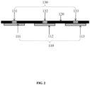
- FIG. 2 is a schematic diagram illustrating another exemplary sensor according to some embodiments of the present disclosure.
- the sensor 100 may include a plurality of sensing elements 110.
- the sensor 100 may also include a plurality of conductive structures 130 having the same count as the sensing elements 110.
- the plurality of conductive structures 130 and the plurality of sensing elements 110 are in one-to-one correspondence.
- the housing 120 is provided with an aperture portion corresponding to each of the plurality of conductive structures 130.
- one end of the conductive structure 130 is electrically connected with a corresponding sensing element 110, and the other end of the conductive structure 130 extends to the outer surface of the housing 120 through its corresponding aperture portion.
- the end of the conductive structure 130 away from the sensing element 110 is exposed to the external environment of the housing 120, so that the user's finger may be in direct contact with a portion of the conductive structure 130 exposed to the external environment of the housing 120 during the touch operation, thereby enabling the human body impedance to be connected to the circuit.
- the conductive structure 130 may be in interference contact with the inner wall of its corresponding aperture portion to ensure the sealing performance and the waterproof performance of the sensor 100.
- the cross-sectional area of the end of the conductive structure 130 that extends to the outer surface of the housing 120 may be larger than the cross-sectional area of the aperture portion, such that the end of the conductive structure 130 that extends to the outer surface of the housing 120 covers the outer side of the aperture portion.
- a waterproofing process may also be used to treat the connection between the conductive structure 130 and the aperture portion, for example, by filling the connection gap between the conductive structure 130 and the aperture portion with waterproofing adhesive, or the like.
- the conductive structures 130 corresponding to the plurality of sensing elements 110 in the sensor 100 may extend into the external environment of the housing 120, such that the skin of the user may contact the conductive structures 130 exposed to the external environment.
- the sensor 100 may include a first sensing element 111 and a first conductive structure 131 corresponding to the first sensing element 111, a second sensing element 112 and a second conductive structure 132 corresponding to the second sensing element 112, and a third sensing element 113 and a third conductive structure 133 corresponding to the third sensing element 113.
- the housing 120 is provided with aperture portions corresponding to the first conductive structure 131, the second conductive structure 132, and the third conductive structure 133.
- One end of the first conductive structure 131, one end of the second conductive structure 132, and one end of the third conductive structure 133 are electrically connected with the first sensing element 111, the second sensing element 112, and the third sensing element 113, disposed inside or on the inner sidewall of the housing 120, respectively.
- the other ends of the first conductive structure 131, the second conductive structure 132, and the third conductive structure 133 extend to the outer surface of the housing 120 through the corresponding aperture portions.
- the senor 100 shown in FIG. 2 is illustrative only, and in some other embodiments, the count of the sensing element 110 and the count of the conductive structure 130 may be, but is not limited to, three. In some embodiments, the count of the sensing elements 110 and the count of the conductive structures 130 may also be 2, 4, 5, or more.
- the plurality of sensing elements 110 may be arranged in an array or a non-arrayed arrangement. In some embodiments, the plurality of sensing elements 110 may be arranged in a linear row. In some embodiments, the plurality of sensing elements 110 may be arranged in an array. In some embodiments, the plurality of sensing elements 110 may be arranged in an array of regular shapes such as triangles, circles, ovals, etc., or other irregular shapes. In some embodiments, the plurality of conductive structures 130 corresponding to the plurality of sensing elements may be spaced apart from each other. In some embodiments, the plurality of conductive structures 130 may be arranged in the same or a different shape as the plurality of sensing elements 110.
- the plurality of sensing elements 110 are spaced apart when the sensor 100 includes the plurality of sensing elements 110.
- the sensor 100 may further include a processor, which may recognize a gesture of the user in response to time points of the user touching different sensing elements 110.
- the plurality of conductive structures 130 (or sensing elements 110) may be distributed in a straight line, and the user slides along an extension direction of the straight line. During the sliding process of the user's finger, the time points acting on different conductive structures 130 are different, and the time points at which the different sensing elements 110 generate electrical signals are different.
- the processor may determine the gesture (e.g., a direction of sliding) of the user based on the time points at which the different sensing elements 110 generate the electrical signals.
- the gesture e.g., a sliding direction
- the processor controls one or more of the progress (e.g., fast-forward or fast-reverse) of audio or video, the volume level, the sliding of pages, or the like, of the wearable device or electronic device based on the gesture of the user.
- a plurality of conductive structures 130 may be distributed in an array, and during the sliding process of the user's finger, the time points acting on different conductive structures 130 are different, and the time points at which the different sensing elements 110 generate electrical signals are different.
- the processor may determine the gesture of the user based on the time points at which the different sensing elements 110 generate the electrical signals.
- the shape of the trajectory presented by the sliding gesture of the user may be any one or more of a letter (e.g., L, Z, M, V, O, C, U, I, S, N, etc.), an Arabic numeral, a geometrical shape (e.g., a circle, an ellipse, a polygon, etc.), or the like.
- the gesture of the user may be applied to device status (e.g., unlocking or locking the screen), calling shortcut commands, etc., of the wearable device or the electronic device.
- the material of the conductive structure 130 may include, but is not limited to, any one or more of silver, copper, gold, aluminum, nickel, alloy, carbon, or the like.
- a droplet may cover two adjacent conductive structures 130 at the same time if a distance between two adjacent conductive structures 130 is too small. That is, the two adjacent conductive structures 130 are connected by the droplet.
- the other conductive structure 130 may also be indirectly connected with the user's finger through the droplet, thereby affecting the accuracy of the sensor 110 in recognizing the gesture of the user.
- the distance between the two adjacent conductive structures in the plurality of conductive structures 130 may be within a range of 0.05 mm-5 cm. In some embodiments, the distance between the two adjacent conductive structures in the plurality of conductive structures 130 may be within a range of 0.08 mm-3 cm. In some embodiments, the distance between the two adjacent conductive structures in the plurality of conductive structures 130 may be within a range of 0.1 mm-1 cm.
- the droplet may be prevented from simultaneously covering two adjacent conductive structures 130, thereby improving the accuracy of the sensor 110 in recognizing the gesture of the user.
- the housing of the sensor 100 may be provided with a relatively large count of conductive structures 130, so that more gestures of the user may be acquired and the applicability of the sensor 100 may be improved.
- two adjacent conductive structures 130 may have the same distance or different distances.
- a droplet may be prevented from covering a plurality of (e.g., two or more) conductive structures 130 at the same time by controlling the distance between the two adjacent conductive structures 130.
- the diameter of the sweat or water droplet deposited on the surface of the housing 120 is usually less than 5 mm.
- the distance between two adjacent conductive structures 130 may be within a range of 8 mm-1 cm.
- a hydrophobic coating may be applied to the portion of the conductive structure 130 that extends to the outside environment of the housing 120 and/or to the outer surface of the housing 120, to reduce the adhesion force between the liquid and the structure of the conductive structure 130 extending into the outer surface of the housing 120 and/or the outer surface of the housing 120.
- the liquid slides off the outer surface of the housing 120 when the user sweats during exercise or touches water, which prevents the liquid from accumulating on the surface of the housing 120.
- a protruding structure may be provided between two adjacent conductive structures 130 to form a curved surface on the housing 120 between the adjacent conductive structures 130 to prevent the liquid from accumulating at the conductive structures 130.
- the portion of the conductive structure 130 that extends to the outer environment of the housing 120 may be concave downwardly with respect to the outer surface of the housing 120. In such cases, the two adjacent conductive structures 130 are separated by the housing region. The volume of the droplet is usually small.
- the droplet When the droplet accumulates on the outer surface of the housing 120, the droplet usually accumulates at a single conductive structure 130 due to the downward concavity of the conductive structure 130 with respect to the outer surface of the housing 120, thereby preventing the droplet from connecting the two adjacent conductive structures 130.
- the conductivity of the conductive structure 130 may be greater than 10 6 S/m to ensure that the conductive structure 130 has good conductivity, allowing the sensor to have a high response sensitivity when the user performs the touch operation and contacts the conductive structure 130.
- a damping structure may be provided at the end of the conductive structure 130 that extends out of the outer surface of the housing 120.
- the damping structure and the outer surface of the housing 120 may have different roughness.
- the damping structure may include stripes, indentations, etc.
- only a portion of the conductive structures 130 of the plurality of conductive structures 130 of the sensor 100 may extend to the outer surface of the housing 120 and be exposed to the external environment of the housing 120, and the other conductive structures 130 may not extend to the outer surface of the housing 120.
- the conductive structures 130 may be located in the interior chamber of the housing 120 or on the inner sidewall of the housing 120.
- the count of conductive structures 130 that extend to the outer surface of the housing 120 may be within a range of 1-4.
- the conductive structures 130 that extend to the outer surface of the housing 120 may be adjacent conductive structures arranged continuously in the plurality of conductive structures 130, or may be non-adjacent conductive structures at least partially spaced apart from one another in the plurality of conductive structures 130 of the sensor 100.
- the sensor 100 includes the plurality of conductive structures 130 and the plurality of sensing elements 110, and when the sensing elements 110 are the capacitive sensing elements, one of the plurality of conductive structures 130 may extend to the outer surface of the housing 120, and the other conductive structures 130 may be disposed in the interior chamber of the housing 120 or on the inner sidewall of the housing 120.
- the droplet may be avoided from covering the plurality of conductive structures 130 at the same time.
- the conductive structure 130 in the sensor 100 that extends to the outer surface of the housing 120 may be provided on a side of the wearable device that is close to the skin of the user for detecting the wearable state. In some embodiments, the conductive structure 130 in the sensor 100 that extends to the outer surface of the housing 120 may be provided on the side of the wearable device that is away from the skin of the user, or other positions that allow for a touch operation in a wearing state for touch operation. A count of the conductive structure 130 in the sensor 100 that extends to the outer surface of the housing 120 may be one or more when applied to wearable detection. When applied to touch operation, the count of the conductive structure 130 in the sensor 100 that extends to the outer surface of the housing 120 may be one or more.
- the wearable device may be controlled by pressing (e.g., a long press) and tapping (e.g., a single click, a double click, etc.).
- pressing e.g., a long press
- tapping e.g., a single click, a double click, etc.
- the user gesture may be recognized by the plurality of conductive structures 130 acting on different sensing elements 110 to control the wearable device.
- the side of the wearable device that is close to the skin of the user refers to a side of the wearable device that is close to the skin of the user in the wearing state.
- the side of the wearable device that is away from the skin of the user refers to a side of the wearable device that is away from the skin of the user in the wearing state.
- the wearable device includes a headphone, a smart watch, a smart bracelet, a smart ring, smart glasses, a smart helmet, a virtual reality device, an augmented reality device, or the like.
- the user's finger may sequentially contact at least two of the plurality of conductive structures 130, and the sensors may sequentially generate electrical signals in the order of contact.
- the processor may determine the gesture of the user based on the position information of the contacted sensors and the time point at which the electrical signals are generated.
- the conductive structures 130 when applied to wearable detection, may be provided on a contact region of the wearable device.
- the contact region refers to a region that may be in contact with the skin of the user when the wearable device is worn.
- a wearing part When the wearable device is worn, a wearing part is in contact with the contact region, which may lead to deformation of the contact region, and the sensor generates a corresponding electrical signal.
- the wearing state of the wearable device may be determined by combining the deformation of the contact region and the electrical signal generated by the sensor.
- the sensing element 110 may include a capacitive sensing element. Electrodes of the capacitive sensing element are electrically connected to an end of the conductive structure 130 disposed inside the housing 120, and the capacitance value may change in response to the finger or skin of the user contacting the conductive structure 130.
- the conductive structure 130 and the electrodes of the capacitive sensing element to which it is connected may be two separate structures or a one-piece structure.
- the conductive structure 130 may be an element independently disposed with respect to the electrodes of the capacitive sensing element, and one end of the conductive structure 130 is electrically connected to an electrode plate of the capacitive sensing element.
- the conductive structure 130 may be part of the electrodes of the capacitive sensing element.
- the conductive structure 130 is integrally structured with an electrode plate of the capacitive sensing element, and the conductive structure 130 is a protruding structure on one side of the electrode plate. That is, a portion of an electrode plate of the capacitive sensing element may be exposed to the external environment of the housing 120. In some embodiments, one side of the electrode plate of the capacitive sensing element may be completely exposed to the external environment of the housing 120, and another electrode plate of the capacitive sensing element may be located inside or on the inner sidewall of the housing 120.
- an electrode plate of the capacitive sensing element is embedded in a sidewall of the housing 120, at which point the electrode plate may be considered as a part of the sidewall of the housing 120.
- the conductive structure such as the conductive structure 130 illustrated in FIG. 3 , is replaced with the first electrode 1101.
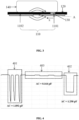
- FIG. 3 is a schematic diagram illustrating another exemplary sensor according to some embodiments of the present disclosure.
- the electrodes of the capacitive sensing element may include a first electrode 1101 and a second electrode 1102, with the first electrode 1101 and the second electrode 1102 disposed in the housing 120.
- one side of the first electrode 1101 and one side of the second electrode 1102 may be connected to an inner surface of the same sidewall of the housing 120, and the first electrode 1101 and the second electrode 1102 are spaced apart along the inner surface of the same sidewall of the housing 120.
- the conductive structure 130 may be electrically connected to one of the first electrode 1101 or the second electrode 1102.
- the finger 140 of the user may be in contact with the conductive structure 130, thereby allowing the human body impedance to be connected to the circuit.
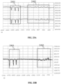
- FIG. 4 is a schematic diagram illustrating a response waveform of an exemplary sensor according to some embodiments of the present disclosure.
- the waveform 401 is a response waveform generated by the sensor during the touch operation using a dry finger in some embodiments, wherein a capacitance change ⁇ C is about 1.892 pF.
- the waveform 402 is a response waveform generated when a concentrated saline droplet is used to cover two electrodes at the same time, wherein a capacitance change ⁇ C is about 1.250 pF.
- the waveband 403 is a response waveform generated by the sensor when the electrodes are covered with purified water, saline, and concentrated saline, wherein a capacitance change of ⁇ C is about 0.164 pF.
- a capacitance change of ⁇ C is about 0.164 pF.
- FIG. 4 there is a significant difference between the response generated in the touch operation using the finger and the response generated when the electrodes are wetted with water (e.g., pure water, saline, or concentrated saline).
- water e.g., pure water, saline, or concentrated saline.
- signal saturation may be generated, which may cause some interference with the recognition of the touch operation.
- the liquid should be located on a single electrode (e.g., the first electrode 1101 or second electrode 1102) as much as possible.
- the droplet may be avoided from covering a plurality of (e.g., two or more) electrodes simultaneously by optimizing an electrode size and a distance between two adjacent electrodes.
- the size (e.g., length) of a single electrode may be within a range of 2 mm-5 mm, and the distance between two adjacent electrodes may be within a range of 8 mm-10 mm.
- a hydrophobic coating may be applied to the outer surface of the housing 120 to reduce the adhesion force between the liquid and the end of the conductive structure 130 protruding out of the outer surface of the housing 120 and/or the outer surface of the housing 120.
- the liquid may slide off the surface of the housing 120 to avoid accumulation of liquid on the surface of the housing 120.
- the plurality of electrodes may be arranged in a direction different from the sliding direction of the liquid in the wearing state.
- the droplet of the liquid slides downwards along a direction that is approximately perpendicular to the ground under the influence of gravity.
- a wearable device e.g., a headphone
- the two electrodes of the sensor 100 may be spaced apart in a direction that is parallel to the ground.
- a protruding structure may be provided on the housing 120 between two adjacent electrodes to block the flow of the droplet.
- droplets are free to flow in a flat plane, and providing the protruding structure on the housing 120 between two adjacent electrodes or setting the portion of the housing to a curved surface structure protruding toward the outside of the housing, the droplets at a single electrode may be blocked from flowing toward the other electrode, thereby effectively avoiding the droplets from covering two electrodes of a single sensor at the same time.
- a shield may be provided between electrodes and voltage may be applied to the shield such that when the sensor scans other buttons, the voltage of the shield is consistent with the voltage of the electrodes, which may minimize the effect of droplets on the electrodes.
- FIG. 5 is a schematic diagram illustrating another exemplary sensor according to some embodiments of the present disclosure.
- the electrodes of the capacitive sensing element may include a first electrode 1101 and a second electrode 1102.
- the first electrode 1101 and the second electrode 1102 are disposed in the interior of the housing 120.
- a first side A of the first electrode 1101 faces a side (e.g., a side B) of the second electrode 1102. That is, a projection of the first electrode 1101 in a direction perpendicular to the first side A of the first electrode 1101 overlaps at least partially with the second electrode 1102.
- first electrode 1101 and the second electrode 1102 have sheet-like structures, and the first side A is a sidewall with the largest area among the sidewalls of the first electrode 1101. Similarly, the side of the second electrode 1102 is a sidewall with the largest area among the sidewalls of the second electrode 1102.
- the first electrode 1101 may be connected to the inner surface of the housing 120, and the second electrode 1102 may be disposed in an interior chamber of the housing 120.
- the second electrode 1102 is disposed parallel or approximately parallel relative to the first electrode 1101, and there is a distance between the two to constitute the capacitive sensing element.
- the finger 140 of the user is not in direct contact with the first electrode 1101 and the second electrode 1102, but can change the capacitance value of the capacitive sensing element constituted by the first electrode 1101 and the second electrode 1102.
- the first electrode 1101 may also not be connected to the inner surface of the housing 120.
- the first electrode 1101 or the second electrode 1102 may be provided in an interior chamber of the housing 120 by a fixed structure (e.g., a bracket).
- the first electrode 1101 may be attached to an inner surface of the housing 120 or at least partially embedded in an inner wall of the housing 120.
- a thickness of the housing 120 in a region corresponding to the first electrode 1101 may be not greater than 1 mm.
- the thickness of the sidewall of the housing 120 in the region corresponding to the first electrode 1101 in a direction perpendicular to the first electrode 1101 is not greater than 1 mm, thereby ensuring the sensitivity of the sensor without exposing the electrode.
- the first electrode 1101 may not take up too much space, making the sensor as small as possible. If the thickness of the sidewall of the housing 120 in the region corresponding to the first electrode 1101 is too small, the stability of the sidewall of the housing 120 may be affected and the sidewall may be prone to damage. To ensure that the sensor has a high sensitivity without exposing the electrode and to ensure the stability of the sidewall of the housing 120, in some embodiments, the thickness of the sidewall of the housing 120 in the region corresponding to the first electrode 1101 may be within a range of 0.2 mm-1 mm.
- FIG. 6 is a schematic diagram illustrating another exemplary sensor according to some embodiments of the present disclosure.
- the electrodes of the capacitive sensing element may include a first electrode 1101 and a second electrode 1102.
- the first electrode 1101 and the second electrode 1102 are located inside the housing 120.
- a first side A of the first electrode 1101 faces a side (e.g., a side B) of the second electrode 1102. That is, a projection of the first electrode 1101 in a direction perpendicular to the first side A of the first electrode 1101 overlaps at least partially with the second electrode 1102.
- a side e.g., a side B
- first electrode 1101 and the second electrode 1102 there is a distance between the first electrode 1101 and the second electrode 1102, and the first electrode 1101 and the second electrode 1102 may form a capacitive sensing element.
- one side of the first electrode 1101 may be directly connected with an inner surface of the housing 120 or embedded in a sidewall of the housing 120.
- the first electrode 1101 and the second electrode 1102 may not be connected to the inner surface of the housing 120.
- the first electrode 1101 and the second electrode 1102 may be fixed in an interior chamber of the housing by a fixing structure (e.g., a bracket, etc.).
- the distance between the first electrode 1101 and the second electrode 1102 may be within a range of 8 mm-10 mm.
- one end of the conductive structure 130 is electrically connected to the first electrode 1101, the other end of the conductive structure 130 may extend out of the inner surface of the housing 120, and the other end of the conductive structure 130 is concave downwardly with respect to the outer surface of the housing 120.
- two adjacent conductive structures 130 are separated by a housing region between the two adjacent conductive structures 130.
- the volume of a droplet is usually small, and when the droplet accumulates on the outer surface of the housing 120, since the conductive structures 130 are concave downwardly relative to the outer surface of the housing 120, the droplet accumulates at a single conductive structure 130, thereby preventing the droplet from connecting the two adjacent conductive structures 130.
- the other end of the conductive structure 130 may protrude out of the outer surface of the housing 120 such that a portion of the conductive structure 130 may be exposed to the external environment of the housing 120 for user contact. Further, the other end of the conductive structure 130 may extend out of the housing 120 until it protrudes out of the outer surface. When the other end of the conductive structure 130 protrudes with respect to the outer surface of the housing 120, the user may quickly determine the distribution position of the conductive structure 130 based on the sense of touch, to perform the relevant operation.
- the sensor 100 may further include a processor that may determine whether the user is contacting the sensor based on a capacitance change value of the capacitive sensing element.
- the processor determining whether the user is contacting the sensor based on the capacitance change value of the capacitive sensing element may include: when the capacitance change value of the capacitive sensing element is greater than a predetermined threshold, determining that the user is contacting the sensor, or when the capacitance change value of the capacitive sensing element is less than the preset threshold, determining that the user is not contacting the sensor.
- the count of the sensing element 110, the count of the conductive structure 130, and the count of other elements in the sensor shown in FIG. 3 to FIG. 6 are not limited to one shown in the drawings but may be multiple. More description regarding the distribution of the plurality of sensing elements 110 or the conductive structures 130 may be found in FIG. 2 of the present disclosure and its related descriptions and will not be repeated herein.
- FIG. 7 is a schematic diagram illustrating a response waveform of another exemplary sensor according to some embodiments of the present disclosure.
- the response waveform is shown as waveform 701.
- the response waveform is shown as waveform 702.
- the touch operation response of the finger of the user may be greatly different from the response generated when the sensor is wet but not touched by the finger, which may eliminate the influence of liquid such as water or sweat on the touch operation, thereby improving the touch sensitivity of the sensor.
- the capacitive sensing element when the sensing element is a capacitive sensing element, the capacitive sensing element may be connected with a measurement circuit to obtain a capacitance change value of the capacitive sensing element.
- the measurement circuit obtaining the capacitance change value of the capacitive sensing element is described in detail in the following in conjunction with FIGs. 8 to FIG. 10 .
- FIG. 8 is a schematic diagram illustrating a circuit structure of an exemplary sensor according to some embodiments of the present disclosure.
- a capacitive element C1 and a capacitive element C2 may be included in the circuit structure of the sensor.
- C1 denotes a capacitor formed by the first electrode 1101 and the second electrode 1102 as shown in FIG. 3 , FIG. 5, or FIG. 6
- the capacitive element C2 denotes the equivalent capacitor corresponding to the human body impedance when it is connected to the circuit.
- the finger 140 of the user may both change the capacitance value of the capacitive element C1 and introduce the capacitive element C2 into the circuit (i.e., to introduce the human body impedance) when the finger 140 of the user performs the touch operation.
- the capacitive element C2 in the circuit is considered to be absent, and only the capacitance value of the capacitive element C1 may be changed.
- the difference between the capacitance value generated when the finger of the user contacts the conductive structure 130 and the capacitance value generated when the water, sweat, or other liquids contacts the conductive structure 130 may be increased, which eliminates the influence of water, sweat, or other liquids on the touch operation and increases the touch sensitivity of the sensor after being wetted with water.
- FIG. 9 is a schematic diagram illustrating a circuit structure of another exemplary sensor according to some embodiments of the present disclosure.
- the measurement circuit of the sensor may include a resistive element R0, a resistive element R1, a capacitive element C3, and a capacitive element C4.
- the capacitive element C3 denotes the capacitive sensing element formed by the first electrode 1101 and the second electrode 1102 as shown in FIG. 3 , FIG. 5, or FIG. 6 .
- the capacitive element C4 denotes the equivalent capacitive element corresponding to the human body impedance when the human body impedance is connected to the circuit.
- the resistive element R0 denotes the equivalent resistance corresponding to the human body impedance when the human body impedance is connected to the circuit. As shown in FIG. 9 , the resistive element R0 may be connected in parallel with the capacitive element C4, and the resistive element R1 and the capacitive element C3 may be connected in series with the capacitive element C4, thereby forming an RC circuit. In some embodiments, the resistive element R0, the capacitive element C4, and the capacitive element C3 may form a capacitor Ct, which may reflect the overall capacitance change in the circuit after the human body impedance is connected to the circuit. In some embodiments, the RC circuit may be used to obtain the capacitance value of the capacitor Ct.
- the measurement circuit of the sensor may further include an inductive element, a capacitive element, and a processing chip.
- the inductive element and the capacitive element are connected in parallel to form a loop, and the processing chip may be configured to read a resonant frequency of the loop formed by the inductive element and the capacitive element.
- the capacitance value of the capacitor Ct may be characterized by the resonant frequency of the loop formed by the inductive element and the capacitive element in the parallel connection.
- the loop formed by the inductive element and the capacitive element may be equivalent to a resonance circuit, which may face the position of the capacitive sensing element to obtain the resonant frequency of the capacitive sensing element.
- the resonance circuit may include a first inductive element L0, a first capacitive element C0, and a first processing chip.
- the first inductive element L0 is connected with the first capacitive element C0 in parallel to form a loop, and the first processing chip is configured to read out a resonant frequency of the loop.
- FIG. 10 is a schematic diagram illustrating a circuit structure of another exemplary sensor according to some embodiments of the present disclosure.
- the measurement circuit of the sensor may include a resistive element R2 and a capacitive element C5.
- the resistive element R2 is connected in parallel with the capacitive element C5 to form an RC loop.
- the capacitance value of the capacitor Ct may be changed.
- the capacitor Ct may be understood as the equivalent capacitor formed by the human body impedance when it is connected to the circuit together with a built-in capacitive sensing element in the sensor. More descriptions regarding the capacitor Ct may be found elsewhere in the present disclosure and may not be repeated here.
- the RC loop formed by the resistive element R2 and the capacitive element C5 in parallel may be configured to obtain the capacitance value of the capacitor Ct.
- the sensing element 110 may include an inductive sensing element, which may include an inductive element, a capacitive element, and a processing chip.
- the inductive element is electrically connected with one end of the conductive structure 130 disposed inside of the housing 120, and the inductive element is connected in parallel with the capacitive element to form a loop.
- the processing chip may be connected to the loop formed by the inductive element and the capacitive element to read a resonant frequency of the loop. In some embodiments, the processing chip may recognize a touch operation of the user based on the resonant frequency of the loop.
- the count of the inductive elements may be one or more (e.g., two or more).
- the sensor 100 may also include a plurality of conductive structures 130 having the same count as the inductive elements, and the plurality of conductive structures 130 and the plurality of inductive elements are in one-to-one correspondence.
- the sensing element 110 is an inductive sensing element
- the sensor 100 may also be configured for wear detection or touch operation detection.
- the count of the inductive sensing elements may be only one.
- the count of the inductive sensing elements may be one or more.
- the count of the inductive sensing elements may be at least two.
- the touch control operation is a single click, a double click, etc.
- the count of the inductive sensing elements may be only one.
- Embodiments of the present disclosure also provide a wearable device that may include a wearable device body and a sensor as provided in any of the above embodiments.
- the wearable device body refers to the remaining body portion without the sensor.
- the wearable device body may include at least a carrier structure, which may be configured to carry the sensing element of the sensor.
- the sensing element may be disposed in an interior chamber or on an inner sidewall of the carrier structure, and one end of the conductive structure away from the sensing element may extend to an outer surface of the carrier structure.
- the carrier structure may be understood as a structure or part that has a certain degree of rigidity and is used to mount the sensor.
- the carrier structure may refer to the housing of the wearable device. Descriptions regarding the position of the conductive structure relative to the carrier structure may be found in the descriptions regarding the conductive structure relative to the housing, which will not be repeated here.
- the user can directly contact the conductive structure with the finger when performing a touch operation, such that the human body impedance may be connected to the electric circuit, which increases the difference between the capacitance value generated when the user's finger is in contact with the conductive structure and the capacitance value generated when the water, sweat, or other liquids is in contact with the conductive structure, thereby eliminating the effect of water, sweat, or other liquids on the touch operation, thus improving the touch sensitivity of the wearable device wetted with water. More details regarding the sensor may be found elsewhere in the present disclosure (e.g., FIGs. 1-10 , and their related descriptions) and will not be repeated here.
- the wearable device may include a headphone, a smart bracelet, a smart ring, smart glasses, a smart helmet, a virtual reality device, an augmented reality device, or the like. It should be understood that the above wearable device is only an exemplary illustration, and in embodiments of the present disclosure, the wearable device may include, but is not limited to, the foregoing devices.
- FIG. 11 is a schematic diagram illustrating an exemplary wearable device according to some embodiments of the present disclosure.
- the wearable device may be an acoustic output device 200, and the wearable device body may include an acoustic output unit 210 and an ear hook 220.
- One end of the ear hook 220 is connected to the acoustic output unit 210, and the user may hang the acoustic output unit 210 near the user's ear via the ear hook 220 when using the acoustic output device 200.
- the conductive structure 130 may be provided on any one or more of the inner, outer, and circumferential sides of the housing of the acoustic output unit 210.
- the inner side refers to a side that is close to the skin of the user when the acoustic output device 200 is worn by the user
- the outer side refers to a side that is away from the skin of the user when the acoustic output device 200 is worn by the user
- the circumferential side refers to the side that is adjacent to either the inner or outer side of the acoustic output unit 210.
- the conductive structure 130 when the user wears the acoustic output device 200, the conductive structure 130 provided at the outer side or the circumferential side of the housing of the acoustic output unit 210 that is not in contact with the skin of the user may be used for touch operation. In some embodiments, the conductive structure 130 may be provided on the outer side of the housing of the acoustic output unit 210 so that the user's hand can act on the sensor.
- the inclination angle of a side surface corresponding to the outer side of the housing of the acoustic output unit 210 relative to the sagittal plane of the human body is extremely small or approximately regarded as parallel, and the droplets at the outer side of the acoustic output unit 210 slide down directly under the effect of gravity and do not accumulate, thereby reducing the interference of the droplets on the sensor.
- the touch operation may include, but is not limited to, clicking, double-clicking, swiping, long pressing, or the like.
- the wearable device may be controlled to perform operations such as waking up the device, answering the phone call, playing the music, adjusting the volume, hanging up the phone call, pausing the music, music switching, audio adjustment, unlocking or locking the device, etc., by the touch operation.
- the user may click on the conductive structure 130 of the sensor to adjust the audio volume output by the acoustic output unit.
- the progress of the audio output from the acoustic output unit may be changed (pause, on, fast-forward, or rewind) or the audio output from the acoustic output unit may be changed.
- the user when sliding along the distribution direction of the conductive structure 130, may adjust the audio volume or the audio progress of the output of the acoustic output unit.
- the sensor may also be configured to detect the wearing state of the acoustic output unit 200.
- the conductive structure 130 when the user is wearing the acoustic output device 200, the conductive structure 130 may be provided on the housing of the acoustic output unit 210 or the ear hook 220 in a region in contact with the skin of the user to perform the wear detection. Specifically, when the acoustic output device 200 is not worn, the conductive structure 130 is not in contact with the human skin, and the sensor does not generate an electrical signal.
- the conductive structure 130 is in contact with the human skin, the sensor generates a corresponding electrical signal, and the processor of the acoustic output device 200 may determine that the acoustic output device 200 is in a wearing state based on the electrical signal, thereby activating or unlocking the acoustic output device 200.
- the ear hook When the conductive structure 130 is provided on the ear hook 220, the ear hook includes a memory alloy (e.g., titanium alloy) strip structure and an adhesive sleeve encasing the strip structure, electrodes corresponding to the conductive structure 130 may be connected to the memory alloy strip structure by adhesive bonding or plating, and at least a portion of the conductive structure 130 may protrude out of the adhesive sleeve to be exposed to the external environment. In some embodiments, at least a portion of the electrodes may be exposed to the external environment when the sensing element is not provided with the conductive structure 130.
- a memory alloy e.g., titanium alloy
- FIG. 12 is a schematic diagram illustrating another exemplary wearable device according to some embodiments of the present disclosure.
- the acoustic output device 200 may also include a rear hook 240, in other words, the acoustic output device 200 may also be a rear-hook earphone, which may include an ear hook 220, a rear hook 240, and an acoustic output unit 210.
- the ear hook 220 may cooperate with the ear contour of the user, so that the acoustic output device 200 may be hung on the ear of the user.
- the rear hook 240 may be placed behind the user's neck or head.
- the ear hook 220 and the rear hook 240 may cooperate to provide a clamping force for wearing the acoustic output unit 210 on the user's head or ear so that the acoustic output device 200 may be stably hung on the user's ear and not easily fall off.
- the acoustic output unit 210 may include a first acoustic output unit 2101 and a second acoustic output unit 2102.
- the ear hook 220 may include a first ear hook 2201 and a second ear hook 2202.
- the first ear hook 2201 is connected to the first acoustic output unit 2101 and one end of the rear hook 240
- the second ear hook 2202 is connected to the second acoustic output unit 2102 and the other end of the rear hook 240.
- the first ear hook 2201 may be configured to hang the first acoustic output unit 2101 near one ear of the user, and the second ear hook 2202 may be configured to hang the second acoustic output unit 2102 near the other ear of the user.
- the wearable device body may further include a core assembly 250, which may be disposed between the ear hook 220 and the rear hook 240.
- the core assembly 250 may include an accommodating cavity that may be configured to hold or accommodate one or more components (e.g., a processor, a control circuit, a Bluetooth module, a battery, etc.) of the acoustic output device 200.
- the core assembly 250 may include a first core assembly 2501 and a second core assembly 2502. The first core assembly 2501 is connected to the first ear hook 2201 and one end of the rear hook 240, and the second core assembly 2502 is connected to the second ear hook 2202 and the other end of the rear hook 240.
- the conductive structure 130 may be disposed on an inner, outer, or circumferential side of the core assembly 250. Specifically, when the conductive structure 130 is provided on the inner side of the core assembly 250, wear detection may be performed through the conductive structure 130. When the conductive structure 130 is provided on the outer or the circumferential side of the core assembly 250, touch operation may be performed through the conductive structure 130. Similarly, in some embodiments, the conductive structure 130 may be provided on the inner, outer, or circumferential side of the acoustic output unit 210. Specifically, when the conductive structure 130 is provided on the inner side of the acoustic output unit 210 that is in contact with human skin, wear detection may be performed through the conductive structure 130.
- touch operation may be performed through the conductive structure 130. More descriptions regarding the conductive structure 130 may be found elsewhere in the present disclosure, and will not be repeated here.
- the wearable device may further include a second inductive sensing element (not shown in the figure), which may have the same structure as the first inductive sensing element.
- the second inductive sensing element may be disposed on the ear hook 220 or the rear hook 240, and the second inductive sensing element may determine the deformation amount of the ear hook 220 or the rear hook 240 based on the deformation of the ear hook 220 or the rear hook 240.
- the deformation amount of the ear hook 220 or the rear hook 240 may be determined based on the inductance change of the second inductive sensing element caused by the deformation of the ear hook 220 or the rear hook 240.
- the processor of the wearable device may determine the wearing state of the wearable device based on the deformation amount of the ear hook 220 or the rear hook 240 detected by the second inductive sensing element.
- FIG. 13 is a schematic diagram illustrating another exemplary wearable device according to some embodiments of the present disclosure.
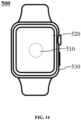
- the wearable device may be a cell phone or a tablet, and the cell phone or tablet computer 300 may include a display 320 and a body 330, with the display 320 embedded in the body 330.
- the sensor may be provided in a touch region 310 of the cell phone or tablet 300.
- the touch region 310 may be understood as an operation region where the user performs the touch operation.
- the touch region 310 may be located on a side of the body 330 that is coplanar with the display 320.
- the touch region 310 may be disposed on a side of the body 330 that is adjacent or opposite to the plane on which the display 320 is located. In some embodiments, the touch region 310 may also be integrated into the display 320. The user may control the cell phone or tablet 300 by acting on the touch region 310 by tapping, long pressing, or swiping.
- the user acts on the touch region 310 to wake up the cell phone or tablet 300 or put it into a standby mode.
- the user may long press on the touch region 310 to turn the cell phone or tablet 300 on or off.
- the user may act on the touch region 310 to adjust the volume of the cell phone or tablet 300.
- the user may act on the touch region 310 to start a voice call or a video call on the cell phone or tablet 300.
- the user may act on the touch region 310 to adjust the progress of the video or audio.
- one or more sensors may be provided at the touch region 310.
- the touch region 310 may include a first sensor and a second sensor, and the user acts on the first sensor by tapping or pressing, etc., to advance the progress of the video or audio.
- a control gesture of the user may be recognized through a plurality of sensors provided in the touch region 310.
- the plurality of sensors may be distributed in the form of a rectangle, triangle, or any combination thereof, and the user swipes through at least two sensors in the touch region 310 to realize different functional controls of the cell phone or tablet 300.
- the user may control the progress of the video or audio by controlling the direction of the swipe of the gesture.
- the user may slide a corresponding pattern within the touch region 310 to compare with a preset pattern to unlock the cell phone or tablet 300.
- the user may slide downward within the touch region 310 to realize a downward page turn of the cell phone or tablet 300, and the user may also slide upward within the touch region 310 to realize an upward page turn of the cell phone or tablet 300.
- the user may slide a "Z" shape within the touch region 310 to take a screenshot of the cell phone or tablet 300.
- FIG. 14 is a schematic diagram illustrating another exemplary wearable device according to some embodiments of the present disclosure.
- the wearable device may be a smartwatch 500.
- the smartwatch 500 may include a display 520 and a dial 530, with the display 520 embedded in the dial 530.
- the sensor is disposed in the smartwatch 500 in a similar manner as the sensor disposed in the cell phone or tablet 300.
- the touch region 510 of the smartwatch 500 may be integrated into the display 520 or disposed on a side adjacent to the display 520. The user may control the smartwatch 500 by acting on the touch region 510 by tapping, long pressing, or swiping.
- the user may tap the touch region 510 to wake up the smartwatch 500 or put the smartwatch into a standby mode.
- the user may long press the touch region 510 to turn the smartwatch 500 on or off, or terminate a functional process of the smartwatch 500 (e.g., music switching, App conversion, audio adjustment), etc.
- the touch region 510 may be disposed on a side of the dial 530 away from the display 520 to detect whether the smartwatch 500 is in a wearing state.
- the wearing detection is similar to the wearing detection of the acoustic output device 200.
- the sensors at the touch region 510 may respond to other processes of the smartwatch 500, such as monitoring the heart rate, etc.
- the sensors may respond to other processing processes of the smartwatch 500, such as ending a non-essential process, etc.
- the touch region 510 may include one or more sensors.
- the plurality of sensors may be centrally distributed within the touch region 510 of the smartwatch 500 shown in FIG. 14 .
- the plurality of sensors may be distributed in a rectangle, a triangle, or any combination thereof, and the user may slide through at least two sensors within the touch region 510 to realize different functional controls of the smartwatch 500.
- the user may slide a corresponding pattern within the touch region 510 to compare with a preset pattern to realize the unlocking of the smartwatch 500.
- the user may slide downward within the touch region 510 to realize a downward page turn of the smartwatch 500, and the user may also slide upward within the touch region 510 to realize an upward page turn.
- the user may slide out an "O" shape within the touch region 510 to enable the smartwatch 500 to hang up the phone.
- the wearable device is not limited to the acoustic output device 200, the cell phone or tablet 300, and the smartwatch 500 as described above.
- the wearable device may include other electronic devices, such as a virtual reality device, an augmented reality device, a smart helmet, smart glasses, or the like.
- the sensors provided by embodiments of the present disclosure may be applied to electronic devices other than wearable devices, such as home appliances (e.g., televisions, refrigerators, air conditioners, control switches, smart door locks, etc.).
- home appliances e.g., televisions, refrigerators, air conditioners, control switches, smart door locks, etc.
- the capacitive sensing element in the embodiments of the present disclosure may also include at least one detecting end, which may be electrically connected with the circuits of the sensor.
- the detecting end may be a structure made of a conductive material (e.g., made of copper, aluminum, silver, carbon, etc.). The following is illustrated in conjunction with FIG. 15A and FIG. 15B .
- FIG. 15A and FIG. 15B The following is illustrated in conjunction with FIG. 15A and FIG. 15B .
- the capacitive sensing element 1501 may include a first electrode 151 and a second electrode 152 provided side by side, and a dielectric 153 provided between the first electrode 151 and the second electrode 152.
- the capacitive sensing element may include two detecting ends, and the two detecting ends are electrically connected with two electrodes of the capacitive sensing element, respectively.
- the human body When the capacitive sensing element 1501 is applied to the sensor, the human body may be approximately equivalent to a capacitor when the human body acts on the capacitive sensing element, the human body capacitance is connected in parallel to the measurement circuit of the sensor.
- the two detecting ends may include a first detecting end 154 and a second detecting end 155.
- the capacitive sensing element 1502 shown in FIG. 15B has substantially the same structure as the capacitive sensing element 1501 shown in FIG. 15A . The difference is that the capacitive sensing element 1502 shown in FIG.
- the first detecting end 154 in the capacitive sensing element 1502 shown in FIG. 15B is not limited to being connected to the first electrode 151, as long as the first detecting end 154 is connected to one of the two electrodes.
- the first detecting end 154 may be connected to the second electrode 152 only.
- FIG. 16A-FIG. 16C are schematic diagrams illustrating exemplary sensors according to some embodiments of the present disclosure.
- the sensor includes a sensing element, the sensing element may be applied to the housing 163, and the housing 163 is configured to carry the sensing element.
- the sensing element may include an electrode 161 and a detecting end 164.
- a count of the detecting end 164 corresponds to a count of the electrode.
- one electrode 161 corresponds to one detecting end 164, one end of the detecting end 164 is connected with the electrode 161, and the other end of the detecting end 164 is connected with the circuit of the sensor.
- the electrode 161 connects the impedance of the body of the user into the sensor when the user is in contact with the electrode 161 or a region of the housing corresponding to the electrode 161.
- the electrode 161 of the sensor 1601 may be embedded in a sidewall of the housing 163, and a portion or all of one side of the electrode 161 may be exposed to the external environment of the housing 163.
- the electrode 161 may also be disposed inside or on the inner sidewall of the housing 163.
- the electrode 161 may be attached to the inner sidewall of the housing 163.
- the electrode 161 may be fixed in the interior chamber of the housing 163 by a fixing structure (e.g., a bracket). As the sensor 1602 shown in FIG.
- one side of the electrode 161 is attached to the inner sidewall in the housing 163, or at least a portion of the electrode 161 is embedded in the inner sidewall of the housing 163, where the connection manner includes, but is not limited to, any one or more of bonding, welding, embedding, or the like.
- the region of the housing 163 corresponding to the electrode 161 may be made of a conductive material (e.g., conductive silicone, copper, aluminum, silver, carbon, etc.) so that human impedance may be connected into the circuit of the sensor when the user contacts the region.
- the electrode 161 when the electrode 161 is provided in the interior chamber of the housing 163, the electrode 161 may be electrically connected with a conductive region of the housing 163 (e.g., the region of the housing 163 corresponding to the electrode 161 described above) via a wire.
- the electrode 161 may include an electrode body 1610 and a conductive structure 165, one end of the conductive structure 165 is electrically connected with the electrode body 1610, the other end of the conductive structure 165 may extend out of an inner surface of the housing 163, and the other end of the conductive structure 165 is concave downwardly with respect to the outer surface of the housing 163.
- the other end of the conductive structure 165 may extend out of the outer surface of the housing 163, such that a portion of the conductive structure 165 may be exposed to the external environment of the housing 163 for user contact.
- the other end of the conductive structure 165 may extend out of the housing 163 until it protrudes from the outer surface. When the end of the conductive structure 165 protrudes relative to the outer surface of the housing 163, the user may quickly determine the distribution position of the conductive structure 165 based on the sense of touch, so as to perform the relevant operation.
- the conductive structure 165 may be an element made of a material having an electrically conductive capability.
- the material of the conductive structure 165 may include, but is not limited to, any one or more of silver, copper, gold, aluminum, nickel, alloy, carbon, or the like.
- the conductive structure 165 may be made of a transparent conductive material, such as an indium tin oxide film, etc.
- the conductive structure 165 may be an element disposed independently with respect to the electrode body 1610.
- one end of the conductive structure 165 is electrically connected with the electrode body 1610.
- the material of the conductive structure 165 may be the same as or different from the material of the electrode body 1610.
- the conductive structure 165 may be a portion of the electrode body 1610.
- the conductive structure 165 and the electrode body 1610 are an integrated structure, and the conductive structure 165 is a protruding structure on one side of the electrode body 1610. In other words, a portion of the electrode body 1610 may be exposed to the external environment of the housing 163.
- FIG. 17 is a schematic diagram illustrating the body of a user in contact with a sensor according to some embodiments of the present disclosure.
- FIG. 18 is a schematic diagram illustrating a droplet acting on a sensor according to some embodiments of the present disclosure.
- FIG. 17 when a finger touches the touch region of the sensor shown in FIG. 16A-FIG. 16C (e.g., the electrode 161 shown in FIG. 16A , the housing 163 with the conductive capability shown in FIG. 16B , or the conductive structure 165 shown in FIG.
- the potential of the finger in the touching system may be considered to be approximated as the potential of the device ground.
- a droplet 168 e.g., salt water
- the droplet 168 may also change the electric field coupling between electrodes 161.
- the surface area of the droplet 161 is much smaller than the human body, the capacitance 166 between the human body and the ground no longer exists, and the capacitance between the droplet 161 and the ground is very small, which is approximated to zero.
- the potential of the droplet 161 in the touch system may not be approximated as the potential of the device ground, and the potential of the droplet 161 is determined by the potential of the electrode 161. It is thus known that when the human body contacts the touch region of the sensor provided in the embodiments of the present disclosure, the human body may form a path with the ground and the device corresponding to the sensor. However, the droplet 168 acting on the touch region of the sensor may not form a path with the device corresponding to the sensor and the earth. Therefore, by measuring the current change in the path formed by the human body, the ground, and the sensor, the human touch and droplet action can be distinguished, thereby preventing the interference of the droplet on the sensor and improving the accuracy of the sensor for human touch control.
- FIG. 19 is a graph illustrating a change curve of a resonant frequency when a finger and a droplet act on the electrodes of a sensor according to some embodiments of the present disclosure.
- the horizontal coordinate denotes the time (ms)
- the vertical coordinate denotes the resonant frequency (Hz).
- the resonant frequency may be used to reflect the amount of the change in capacitance.
- the region 2001 shows the change curve of the resonant frequency corresponding to the electrode of the sensor lightly touched by dry hands
- region 2002 shows the change curve of the resonant frequency corresponding to the electrode of the sensor lightly touched by saltwater droplets
- region 2003 shows the change curve of the resonant frequency corresponding to the electrode of the sensor lightly touched by wet hands.
- the resonant frequency i.e., the capacitance of the sensor
- the resonant frequency when the saltwater droplets act on the electrodes of the sensor has almost no fluctuation.
- the sensor provided by the embodiments of the present disclosure prevents the interference of the droplets on the sensor and improves the accuracy of the sensor for human touch control.
- the count of the sensing elements may be but not limited to two.
- the count of the sensing elements may also be 3, 4, 5, or more.
- the plurality of sensing elements may be arranged in an array or a nonarray.
- the plurality of sensing elements may be arranged in a linear arrangement.
- the plurality of sensing elements may be arranged in an array.
- the plurality of sensing elements may be arranged in a regular shape such as a triangle, a circle, etc., an ellipse, etc., or other irregular shapes.
- the sensing element of the sensor is not limited to the case where the electrodes are disposed inside the housing, but may also be the electrode structure and distribution shown in FIG. 16A and FIG. 16C .
- the plurality of sensing elements are spaced apart.
- the sensor may also include a processor, and the processor may recognize, in response to the time of the user touching different sensing elements, the gesture of the user.
- the droplet may cover the electrodes of two adjacent sensing elements at the same time.
- the two adjacent electrodes are connected by the droplet, and the two adjacent electrodes and the droplet form a structure similar to a capacitive structure, thus forming an additional capacitance field.
- the touch signal of the sensor when the human body touches (tapping or sliding) different electrodes may be submerged, making the sensor unable to distinguish between the human touch and the droplet action.
- the processor may also use a signal differential processing to minimize the effect of the droplet covering two adjacent electrodes.
- the sensor may include a first electrode and a second electrode.
- the signal differential processing may include obtaining a first electrical signal change value corresponding to the first electrode and a second electrical signal change value corresponding to the second electrode and determining a touch manner of the user based on difference information between the second electrical signal change value and the first electrical signal change value.
- the difference information may include a difference magnitude and a positive or negative of the difference.
- the sensor having two electrodes i.e., the sensor having two sensing elements
- the two electrodes may include a first electrode and a second electrode disposed sequentially from top to bottom along a spatial direction, the first electrical signal change value corresponding to the first electrode and the second electrical signal change value corresponding to the second electrode are obtained, and the difference between the second electrical signal change value and the first electrical signal change value is calculated.
- the first electrical signal change value generated by the first electrode is A1
- the second electrical signal change value corresponding to the second electrode is 0.
- the difference information between the second electrical signal change value and the first electrical signal change value is -A1.
- the second electrical signal change value generated by the second electrode is A2
- the first electrical signal change value corresponding to the first electrode is 0.
- the difference information between the second electrical signal change value and the first electrical signal change value is A2.
- the difference information between the second electrical signal change value and the first electrical signal change value changes from A2 to - A1; and when the user slides downwards and contacts the first electrode first and then the second electrode, the difference information between the second electrical signal change value and the first electrical signal change value changes from -A1 to A2.
- the saltwater droplet covers both the first electrode and the second electrode, or when the saltwater droplet is located at one of the first electrode or the second electrode, the difference information remains unchanged, as shown in FIG. 21.
- Region 2201 shows the change curve of the electrical signal corresponding to the first electrode of the sensor touched lightly by a finger
- region 2202 shows the change curve of the electrical signal corresponding to the second electrode of the sensor touched lightly by a finger
- region 2203 shows the change curve of the electrical signal corresponding to sliding the first electrode and the second electrode of the sensor downward with a finger
- region 2204 shows the change curve of the electrical signal corresponding to sliding the second electrode and the first electrode of the sensor upward with a finger
- region 2205 shows the change curve of the electrical signal corresponding to applying the saltwater droplet to one of the second electrode or the first electrode of the sensor
- region 2206 shows the change curve of the electrical signal corresponding to applying the saltwater droplet to the second electrode and the first electrode of the sensor.
- the electric signal remains unchanged when the saltwater droplet is applied to a single electrode of the sensor, and the fluctuation of the electric signal is very small when the saltwater droplet is applied to the first electrode and the second electrode of the sensor at the same time.
- the electrodes of the sensor are touched or slid by a finger, the electrical signal has obvious changes.
- a sensing element having a conductive structure as illustrated in FIG. 16C may be used, and a distance between two adjacent conductive structures 165 of the plurality of conductive structures 165 may be within a range of 0.05 mm-5 cm.
- the distance between two adjacent conductive structures in the plurality of conductive structures 165 may be within a range of 0.08 mm-3 cm.
- the distance between two adjacent conductive structures 165 in the plurality of conductive structures 165 may be within a range of 0.1 mm-1 cm.
- the distance between two adjacent conductive structures 165 may be the same or different.
- the droplet may be prevented from covering a plurality (e.g., two or more) of conductive structures 165 at the same time by controlling the distance between two adjacent conductive structures 165.
- the diameter of the sweat or droplets deposited on the surface of the housing 163 is less than 5 mm. Based on this, in order to avoid a single droplet covering a plurality of (e.g., two or more) conductive structures 165 at the same time, the distance between two adjacent conductive structures 165 may be within a range of 8 mm-1 cm.
- a hydrophobic coating may be applied to the end of the conductive structure 165 that extends out of the outer surface of the housing 163 and/or to the outer surface of the housing 163 to reduce the adhesion force between the liquid and the end of the conductive structure 165 that extends out of the outer surface of the housing 163 and/or the outer surface of the housing 163.
- the liquid may slide off on the surface of the housing 163, thereby preventing the liquid from accumulating on the surface of the housing 163.
- a protruding structure may be provided between two adjacent conductive structures 165 to form a curved surface of the housing 163 between the adjacent conductive structures 165 to prevent the liquid from accumulating at the conductive structure 165.
- the sensing elements are electrodes
- the sensing elements are electrodes
- the sensing elements are electrodes
- the electrodes are large in size and form a large facing area with the liquid, which makes the signals generated by the sensing elements of the sensor when the wet hair, sweat, etc. act on the sensor very close to and difficult to distinguish from the signals generated by the sensing elements of the sensor when the finger contacts the sensor.
- the facing area in the embodiment of the present disclosure refers to the area where the liquid overlaps with the electrode.
- the electrode may be a needle electrode, and compared with a sheet electrode, the needle electrode may reduce the coupling capacitance caused by the facing area.
- the capacitance of the human body is greater than the capacitance of the sweat, thus enabling the sensor to distinguish between the human touch and sweat accumulation on the sensor, ensuring the accuracy of the sensor in recognizing the user's action.
- FIG. 22 is a graph illustrating change curves of resonant frequencies collected when a finger and wet hair act on two needle electrodes of a sensor according to some embodiments of the present disclosure. As shown in FIG. 22 , the horizontal coordinate denotes the time (ms), and the vertical coordinate denotes the resonant frequency (Hz). As shown in FIG.
- region 2301 shows the change curve of the resonant frequency collected when wet hair is used to lightly touch the needle electrode of the sensor
- region 2302 shows the change curve of the resonant frequency collected when wet hair is used to slide the needle electrode of the sensor
- region 2303 shows the change curve of the resonant frequency collected when the hand is used to lightly touch the needle electrode of the sensor
- region 2304 shows the change curve of the resonant frequency collected when the hand is used to slide on the needle electrode of the sensor.
- the resonant frequency i.e., the amount of change in capacitance of the sensor
- the sensor provided by the embodiment of the present disclosure may prevent the interference of wet hair or wet clothing on the sensor and improve the accuracy of the sensor for human touch control.
- FIG. 23A-FIG. 23D are graphs illustrating change curves of resonant frequencies collected by sensors according to some embodiments of the present disclosure.
- each of the sensors in FIGs. 23A-23D includes two electrodes (e.g., a first electrode and a second electrode).
- the hand and the wet hair of the user slide along the two electrodes of the sensor, respectively.
- Region 2401 in FIGs. 23A-23D shows the change curve of the resonant frequency collected when the hand of the user acts on the electrodes of the sensor
- region 2402 in FIGs. 23A-23D shows the change curve of the resonant frequency collected when the wet hair acts on the electrodes of the sensor.
- the size of the electrodes are progressively larger in size. According to FIG. 23A-FIG. 23D , as the size of the electrodes increases, the change in the resonant frequency collected when the wet hair acts on the electrodes in the sensor becomes more significant. Thus, in order to increase the difference between the effect of the liquid or wet hair on the sensor and the effect of the human hand on the sensor, thus reduce the interference of the wet hair or wet clothing on the sensor in recognizing the touch of the user's hand, the size of the electrode should not be too large.
- the size of the electrode here refers to the area of the electrode exposed to the external environment.
- the electrodes of the sensor may be needle electrodes to reduce the coupling capacitance caused by the facing area.
- the capacitance of the human body is greater than the capacitance of the sweat, so that the sensor may distinguish between the human touch and the sweat accumulation on the sensor, which ensures the accuracy of the sensor in recognizing the user's action.
- the size of the needle electrode along a long axis direction is within a range of 5 mm-50 mm, and the size of the needle electrode along a short axis direction is within a range of 0.1 mm-5 mm.
- the electrodes of the sensor and the liquid form a relatively small facing area, thus increasing the difference between the effect of the liquid or wet hair on the sensor and the effect of the human hand acting on the sensor.
- the size of the needle electrode along the long axis direction is within a range of 10mm-15mm, and the size of the needle electrode along the short axis direction is within a range of 0.5mm-2mm.
- a ratio of the size of the needle electrode along the long axis direction to the size of the needle electrode along the short axis direction may be greater than 2. In some embodiments, the ratio of the size of the needle electrode along the long axis direction to the size of the needle electrode along the short axis direction may be greater than 5 to further reduce the facing area between the electrodes of the sensor and the liquid.
- FIG. 24 is a diagram illustrating a signal of a sensor according to some embodiments of the present disclosure.
- the signal graph read by the measurement circuit of the sensor is not a straight line when the signal is read due to noise fluctuation, zero drift, environmental interference, etc.
- Th2 a specific judgment threshold used to analyze the fluctuation of the resonant frequency to determine whether the user acts on the sensor, there may be a problem of misjudgment and wrong judgment.
- a zero-following algorithm is adopted in some embodiments of the present disclosure to eliminate disturbances caused by noise fluctuation, zero drift, environmental disturbances, etc.
- the processor of the sensor is configured to adjust the zero point based on fluctuation information of the resonant frequency.
- the S1 segment in FIG. 25 is the resonant frequency collected when the user doesn't act on the sensor, wherein the resonant frequency only has small amplitude noise, slow drift.
- the zero point changes with the resonant frequency. For example, the zero point increases as the resonant frequency increases and decreases as the resonant frequency decreases, and the resonant frequency fluctuates over a small range.
- three adjacent data points A 1 , B 1 , and C 1 may be selected in the resonant frequency, and the data changes of two adjacent data points ⁇ 1 and ⁇ 2 may be obtained by calculating a difference between the two adjacent data points, respectively.
- the processor of the sensor is further configured to remain the zero point until falling change information of the electrical signal reaches a minimum value of the electrical signal.
- the body e.g., the finger
- the impedance of the body of the user begins to be connected to the measurement circuit of the sensor.
- the resonant frequency read by the sensor suddenly decreases due to the high impedance of the body of the user.
- the resonant frequency read by the sensor reaches the minimum value.
- the change in the resonant frequency read by the measurement circuit of the sensor is primarily caused by the connection of the impedance of the body of the user, the zero point is kept constant.
- the falling change information of the resonant frequency includes the data change of two adjacent data points. For example, in segment S2, the difference ⁇ 1 between data points A 1 and B 1 is less than the fluctuation threshold Th1, and the difference ⁇ 2 between data points B 1 and C 1 is greater than the fluctuation threshold Th1.
- the difference ⁇ 1 between data points A 1 and B 1 and the difference ⁇ 2 between data points B 1 and C 1 are both less than the fluctuation threshold Th1, and the differences between the zero point corresponding to the end of the segment S1 (also referred to as the zero values before the breakthrough of the resonant frequency), and data points A 1 , B 1 , and C 1 are all greater than a determination threshold Th2.
- the processor of the sensor is further configured to rise the zero point with the resonant frequency based on rising change information of the resonant frequency.
- the body e.g., the finger
- the impedance of the body of the user is no longer connected into the measurement circuit of the sensor.
- the resonant frequency read by the sensor suddenly rises, and the zero point increases with the resonant frequency until the resonant frequency returns to segment S1.
- the falling change information of the resonant frequency includes the data change of two adjacent data points. For example, in segment S3, the difference ⁇ 1 between data points A 1 and B 1 is less than the fluctuation threshold Th1, the difference ⁇ 2 between data points B 1 and C 1 is greater than the fluctuation threshold Th1.
- FIG. 24-FIG.26 are implementations in which a single electrode is provided in the sensor to recognize the user's tapping control operation.
- a plurality of electrodes may be included in the sensor, and a processor of the sensor may recognize a gesture of the user in response to the time points when the user touches the different electrodes.
- the plurality of electrodes may be distributed in a straight line, and the user slides along an extension direction of the straight line. When the user's finger slides, the time points at which it acts on different electrodes are different, and the time points at which the resonance frequencies corresponding to the different electrodes are collected are different.
- the processor may determine the gesture of the user (e.g., the sliding direction) based on the time point at which the resonant frequency of the sensor corresponding to different electrodes changes.
- FIG. 27 is a graph illustrating change curves of resonant frequencies when the hand of a user acts on two electrodes in a sensor according to some embodiments of the present disclosure.
- FIG. 28 is a graph illustrating change curves of resonant frequencies when wet hair acts on two electrodes in a sensor according to some embodiments of the present disclosure. According to FIG. 27 and FIG.
- the change amount of the resonant frequency when the hand of the user acts on the sensor is significantly larger than the change amount of the resonant frequency when the wet hair acts on the sensor.
- the difference between the change amount of the resonant frequency of the electrical signal generated when the hand of the user acts on the sensor and the change amount of the resonant frequency generated when the wet hair acts on the sensor may be further improved, thereby improving the accuracy of the sensor.
- the sensors shown in FIG. 16A-FIG. 28 may be applied to at least one of a headphone, a smart bracelet, a smart ring, smart glasses, a smart helmet, a virtual reality device, or an augmented reality device, for example, the electronic device shown in FIGs. 11-14 .
- beneficial effects that may be produced by different embodiments are different, and the beneficial effects that may be produced in different embodiments may be any one or a combination of any of the foregoing, or any other beneficial effect that may be obtained.
Landscapes
- Engineering & Computer Science (AREA)
- Theoretical Computer Science (AREA)
- General Engineering & Computer Science (AREA)
- Physics & Mathematics (AREA)
- General Physics & Mathematics (AREA)
- Human Computer Interaction (AREA)
- Computer Hardware Design (AREA)
- Power Engineering (AREA)
- Life Sciences & Earth Sciences (AREA)
- Biophysics (AREA)
- General Health & Medical Sciences (AREA)
- Physiology (AREA)
- Health & Medical Sciences (AREA)
- Electronic Switches (AREA)
- Measurement And Recording Of Electrical Phenomena And Electrical Characteristics Of The Living Body (AREA)
Abstract
Description
- The present disclosure relates to the technical field of sensor devices, and in particular, to sensors and wearable devices.
- Touch operation is an important human-computer interaction method for wearable devices. Users can control wearable devices by inputting various control commands to sensors of the wearable devices through touch operations (e.g., swiping, clicking, double-clicking, longpressing, etc.). However, the sensors currently used (e.g., a capacitive sensing element and an inductive sensor) fail to function after being exposed to water, which is not conducive to application in scenarios that are easily contaminated with liquids (e.g., when swimming or in sports scenarios that are prone to sweating) when the sensors are applied to wearable devices.
- Therefore, it is desirable to provide a sensor that may effectively avoid liquid interference.
- One of the embodiments of the present disclosure provides a sensor. The sensor may include a sensing element and a conductive structure. The sensor may be applied to a housing. The housing may be configured to carry the sensing element and the conductive structure, the sensing element may be disposed inside or on an inner sidewall of the housing, at least a portion of the conductive structure may be exposed to an external environment of the housing, and the conductive structure may be electrically connected with the sensing element.
- Embodiments of the present disclosure also provide a wearable device. The wearable device may include a sensor. The sensor may include a sensing element, a conductive structure, and a wearable device body. One end of the conductive structure may be electrically connected with the sensing element. The wearable device body may include at least a carrier structure configured to carry the sensing element and the conductive structure. The sensing element may be disposed inside or on an inner sidewall of the carrier structure, at least a portion of the conductive structure may be exposed to an external environment of the carrier structure, and the conductive structure may be electrically connected with the sensing element.
- One of the embodiments of the present disclosure further provides a sensor including a capacitive sensing element. The capacitive sensing element may be applied to a housing and disposed inside the housing. The capacitive sensing element may include a first electrode and a second electrode. The first electrode may be directly or indirectly connected with an inner surface of the housing and may have a first side, a side of the second electrode may be disposed opposite to the first side, and there may be a distance between the first electrode and the second electrode.
- One of the embodiments of the present disclosure further provides a sensor including a sensing element. The sensing element may be applied to a housing, and the housing may be configured to carry the sensing element. The sensing element may include one or more electrodes and one or more detecting ends. Each electrode of the one or more electrodes may correspond to one detecting end of the one or more detecting ends, one end of the detecting end may be connected with the electrode, and another end of the detecting end may be connected with a circuit of the sensor. When a user is in contact with the electrode or a region of the housing corresponding to the electrode, the electrode and the detecting end may correspond to the electrode wire an impedance of the body of the user into the sensor.
- Additional features may be set forth in part in the following description and may become apparent to those skilled in the art by reference to the following and the accompanying drawings or may be understood by the production or operation of examples. Features of the present disclosure may be realized and obtained by practicing or using aspects of the methods, tools, and combinations set forth in the following detailed examples.
- The present disclosure is further illustrated in terms of exemplary embodiments. These exemplary embodiments are described in detail with reference to the drawings. These embodiments are non-limiting exemplary embodiments, in which like reference numerals represent similar structures, and wherein:
-
FIG. 1 is a schematic diagram illustrating an exemplary sensor according to some embodiments of the present disclosure; -
FIG. 2 is a schematic diagram illustrating another exemplary sensor according to some embodiments of the present disclosure; -
FIG. 3 is a schematic diagram illustrating another exemplary sensor according to some embodiments of the present disclosure; -
FIG. 4 is a schematic diagram illustrating a response waveform of an exemplary sensor according to some embodiments of the present disclosure; -
FIG. 5 is a schematic diagram illustrating another exemplary sensor according to some embodiments of the present disclosure; -
FIG. 6 is a schematic diagram illustrating another exemplary sensor according to some embodiments of the present disclosure; -
FIG. 7 is a schematic diagram illustrating a response waveform of another exemplary sensor according to some embodiments of the present disclosure; -
FIG. 8 is a schematic diagram illustrating a circuit structure of an exemplary sensor according to some embodiments of the present disclosure; -
FIG. 9 is a schematic diagram illustrating a circuit structure of another exemplary sensor according to some embodiments of the present disclosure; -
FIG. 10 is a schematic diagram illustrating a circuit structure of another exemplary sensor according to some embodiments of the present disclosure; -
FIG. 11 is a schematic diagram illustrating an exemplary wearable device according to some embodiments of the present disclosure; -
FIG. 12 is a schematic diagram illustrating another exemplary wearable device according to some embodiments of the present disclosure; -
FIG. 13 is a schematic diagram illustrating another exemplary wearable device according to some embodiments of the present disclosure; -
FIG. 14 is a schematic diagram illustrating another exemplary wearable device according to some embodiments of the present disclosure; -
FIG. 15A is a schematic diagram illustrating an exemplary capacitive sensor according to some embodiments of the present disclosure; -
FIG. 15B is a schematic diagram illustrating another exemplary capacitive sensor according to some embodiments of the present disclosure; -
FIG. 16A is a schematic diagram illustrating another exemplary sensor according to some embodiments of the present disclosure; -
FIG. 16B is a schematic diagram illustrating another exemplary sensor according to some embodiments of the present disclosure; -
FIG. 16C is a schematic diagram illustrating another exemplary sensor according to some embodiments of the present disclosure; -
FIG. 17 is a schematic diagram illustrating a body of a user in contact with a sensor according to some embodiments of the present disclosure; -
FIG. 18 is a schematic diagram illustrating a droplet acting on a sensor according to some embodiments of the present disclosure; -
FIG. 19 is a graph illustrating a change curve of a resonant frequency when a finger and a droplet act on electrodes of a sensor according to some embodiments of the present disclosure; -
FIG. 20 is a schematic diagram illustrating an exemplary sensor according to some embodiments of the present disclosure; -
FIG. 21 is a graph illustrating a change curve of an electrical signal in different touch manners according to some embodiments of the present disclosure; -
FIG. 22 is a graph illustrating change curves of resonant frequencies collected when a finger and wet hair act on two needle electrodes of a sensor according to some embodiments of the present disclosure; -
FIG. 23A is a graph illustrating change curves of resonant frequencies collected by a sensor according to some embodiments of the present disclosure; -
FIG. 23B is a graph illustrating change curves of resonant frequencies collected by another sensor according to some embodiments of the present disclosure; -
FIG. 23C is a graph illustrating change curves of resonant frequencies collected by another sensor according to some embodiments of the present disclosure; -
FIG. 23D is a graph illustrating change curves of resonant frequencies collected by yet another sensor according to some embodiments of the present disclosure; -
FIG. 24 is a diagram illustrating a signal of a sensor according to some embodiments of the present disclosure; -
FIG. 25 is a graph illustrating a change curve of a resonant frequency collected by a sensor with a single electrode according to some embodiments of the present disclosure; -
FIG. 26 is a graph illustrating a change curve of a resonant frequency collected by a sensor with a single electrode according to some embodiments of the present disclosure; -
FIG. 27 is a graph illustrating change curves of resonant frequencies when a hand of a user acts on two electrodes in a sensor according to some embodiments of the present disclosure; and -
FIG. 28 is a graph illustrating change curves of resonant frequencies when wet hair acts on two electrodes in a sensor according to some embodiments of the present disclosure. - To more clearly illustrate the technical solutions related to the embodiments of the present disclosure, a brief introduction of the drawings referred to the description of the embodiments is provided below. Obviously, the drawings described below are only some examples or embodiments of the present disclosure. Those having ordinary skills in the art, without further creative efforts, may apply the present disclosure to other similar scenarios according to these drawings. Unless obviously obtained from the context or the context illustrates otherwise, the same numeral in the drawings refers to the same structure or operation.
- As shown in the present disclosure and claims, the words "one," "a," "a kind," and/or "the" are not especially singular but may include the plural unless the context expressly suggests otherwise. In general, the terms "comprise," "comprises," "comprising," "include," "includes," and/or "including" merely prompt to include operations and elements that have been clearly identified, and these operations and elements do not constitute an exclusive listing. The methods or devices may also include other operations or elements.
- In the description of the present disclosure, it is to be understood that the terms "front," "rear," "ear hook," "rear hook," etc. indicate orientation or positional relationships based on those shown in the accompanying drawings, and are used only for the convenience of describing the present disclosure and simplifying the description, and does not indicate or imply that the device or component referred to must have a specific orientation, be constructed and operated in a specific orientation, and therefore cannot be understood as a limitation of the present disclosure.
- Additionally, the terms "first" and "second" are used for descriptive purposes only and are not to be construed as indicating or implying relative importance or implicitly specifying the number of technical features indicated. Therefore, a feature defined as "first" and "second" may expressly or impliedly include at least one of the features. In the description of the present disclosure, "plurality" means at least two, e.g., two, three, or the like, unless explicitly and specifically limited otherwise.
- In the present disclosure, unless otherwise specified and limited, the terms "mounted," "connected," "connection," "fixed," etc. should be broadly understood, for example, it can be fixed connections, detachable connections, or integrated; it can be a mechanical connection or an electrical connection; it can be directly connected or indirectly connected through an intermediate medium, and can be a connection within two components or an interaction relationship between two components, unless otherwise specified. Those skilled in the art can understand the specific meanings of the above terms in the present disclosure according to the specific situation.
- Embodiments of the present disclosure provide a sensor and a wearable device. The sensor penetrates a sidewall of the housing through a conductive structure, making one end of the conductive structure electrically connected with the sensor and the other end of the conductive structure extend to the outer surface of the housing. Thus, when a user performs a touch operation, the human body impedance may be connected to a measurement circuit of the sensor through the conductive structure to realize the touch operation. Since there is a large difference between the impedance value generated when the human body contacts the conductive structure of the sensor and the impedance value generated when a liquid such as water or sweat contacts the conductive structure of the sensor, the sensor provided by the embodiments of the present disclosure may exclude the influence of water, sweat, or other liquids on the touch operation, and improve the touch sensitivity of the sensor after being exposed to water. In some embodiments, the sensor may be applied to a wearable device, so that when a user manipulates the wearable device, the effect of liquids, such as water, sweat, etc. on the touch operation may be eliminated, and the touch sensitivity of the wearable device may be improved after being exposed to water. Exemplary wearable devices may include headphones, smart bracelets, smart rings, smart glasses, smart helmets, virtual reality devices, augmented reality devices, or the like.
- The sensor and wearable device provided by the embodiments of the present disclosure are described in detail below in connection with the accompanying drawings.
-
FIG. 1 is a schematic diagram illustrating an exemplary sensor according to some embodiments of the present disclosure. - Referring to
FIG. 1 , in some embodiments, thesensor 100 may include asensing element 110 and aconductive structure 130. Thesensing element 110 and theconductive structure 130 are applied to ahousing 120, and thehousing 120 is configured to carry thesensing element 110 and theconductive structure 130. In some embodiments, thesensing element 110 may be disposed inside or on an inner sidewall of thehousing 120. The inner sidewall refers to a sidewall corresponding to an interior chamber of thehousing 120. In some embodiments, at least a portion of theconductive structure 130 is exposed to the external environment of thehousing 120 to be accessible to the skin of a user. In some embodiments, one end of theconductive structure 130 is electrically connected to afirst electrode 1101, the other end of theconductive structure 130 may extend out of an inner surface of thehousing 120, and the other end of theconductive structure 130 is concave downwardly with respect to an outer surface of thehousing 120. When there are a plurality ofconductive structures 130, two adjacentconductive structures 130 are separated by a housing region between the two adjacentconductive structures 130. The volume of a droplet is usually small, and when the droplet accumulates on the outer surface of thehousing 120, the droplet typically accumulates at a singleconductive structure 130, thereby preventing the droplet from connecting the two adjacentconductive structures 130. In some embodiments, the other end of theconductive structure 130 may extend out of the outer surface of thehousing 120 such that a portion of theconductive structure 130 may be exposed to the external environment of thehousing 120 for contact by the user. In some embodiments, the other end of theconductive structure 130 may also extend out of thehousing 120 until it protrudes out of the outer surface. When the other end of theconductive structure 130 protrudes out with respect to the outer surface of thehousing 120, the user may quickly determine the distribution position of theconductive structure 130 based on his/her sense of touch, to perform the relevant operation. When the user touches theconductive structure 130, the human body impedance of the user may be connected with thesensing element 110, and thesensing element 110 may generate a corresponding electrical signal in response to the touch operation of the user. For example, thesensing element 110 may generate a first signal in response to a sliding operation of the user. As another example, thesensing element 110 may generate a second signal in response to a click operation of the user. As yet another example, thesensing element 110 may generate a third signal in response to a double-click or multi-click operation of the user. In some embodiments, thesensing element 110 may include a capacitive sensing element and/or an inductive sensing element. In some embodiments, when thesensing element 110 is a capacitive sensing element, the capacitance value of thesensing element 110 may change in response to contact of the skin of the user (e.g., finger) with theconductive structure 130. Similarly, when thesensing element 110 is an inductive sensing element, the inductance value of thesensing element 110 may change in response to contact of the skin of the user (e.g., finger) with theconductive structure 130. - In some embodiments, the shape of the
housing 120 may be a regular shape such as cylindrical, elliptical column, dome, prismatic (e.g., trigonal, rectangular, pentagonal), or other irregular three-dimensional shapes. In some embodiments, the material of thehousing 120 may include plastic, resin, glass, metal, etc. In some embodiments, thehousing 120 may be made of a transparent material. It should be noted that when thesensor 100 is applied to the wearable device, thehousing 120 may be a structure that is independently disposed with respect to the wearable device, or it may be an integral structure with the wearable device, that is, the wearable device may serve as the housing of thesensor 100. - The
conductive structure 130 may be an element made of a material that conducts electricity. In some embodiments, the material of theconductive structure 130 may include, but is not limited to, any one or more of silver, copper, gold, aluminum, nickel, alloys, carbon, etc. In some embodiments, theconductive structure 130 may be made of a transparent conductive material, such as an indium tin oxide film. In some embodiments, at least a portion of theconductive structure 130 is exposed to the external environment of thehousing 120, and theconductive structure 130 may penetrate the sidewall of thehousing 120 corresponding to theconductive structure 130 and be electrically connected with thesensing element 110 in the interior chamber or on the inner sidewall of thehousing 120. When the user performs the touch operation, the user's finger may be in direct contact with the portion of theconductive structure 130 that is exposed to the external environment of thehousing 120, thereby allowing the human body impedance to be connected with the measurement circuit of thesensor 100. In some embodiments, theconductive structure 130 may be an independently disposed element relative to thesensor element 110. For example, when thesensing element 110 is a capacitive sensing element, one end of theconductive structure 130 is electrically connected with an electrode plate of the capacitive sensing element. In some embodiments, the material of theconductive structure 130 may be the same as or different from the material of thesensing element 110. In some embodiments, theconductive structure 130 may be a portion of thesensor element 110. For example, when thesensing element 110 is a capacitive sensing element, theconductive structure 130 is integrally structured with an electrode plate of the capacitive sensing element, and theconductive structure 130 is a protruding structure on one side of the electrode plate. That is, a portion of an electrode plate of the capacitive sensing element may be exposed to the external environment of thehousing 120. In some embodiments, one side of one electrode plate of the capacitive sensing element may all be exposed to the outside environment of thehousing 120, and an other electrode plate of the capacitive sensing element may be located inside or on the inner sidewall of thehousing 120. For example, one electrode plate of the capacitive sensing element is embedded in the sidewall of thehousing 120, at which point the electrode plate may be considered as a portion of the sidewall of thehousing 120, and, for ease of understanding, theconductive structure 130, as illustrated inFIG. 3 , is replaced with afirst electrode 1101. - It should be noted that since there is a large difference between the impedance value generated when the human body (e.g., the user's finger) contacts the
conductive structure 130 and the impedance value generated when the droplet (e.g., a water droplet, sweat) contacts theconductive structure 130, the effect of liquids on the touch operation may be eliminated by the solution provided by the embodiments of the present disclosure, and a difference between a circuit output when the user contacts theconductive structure 130 and a circuit output when the user does not contact theconductive structure 130 may be increased, thereby increasing the touch sensitivity of the wearable device when exposed to water. -
FIG. 2 is a schematic diagram illustrating another exemplary sensor according to some embodiments of the present disclosure. In some embodiments, thesensor 100 may include a plurality ofsensing elements 110. Correspondingly, thesensor 100 may also include a plurality ofconductive structures 130 having the same count as thesensing elements 110. The plurality ofconductive structures 130 and the plurality ofsensing elements 110 are in one-to-one correspondence. Thehousing 120 is provided with an aperture portion corresponding to each of the plurality ofconductive structures 130. For each of the plurality ofconductive structures 130, one end of theconductive structure 130 is electrically connected with a correspondingsensing element 110, and the other end of theconductive structure 130 extends to the outer surface of thehousing 120 through its corresponding aperture portion. In such cases, the end of theconductive structure 130 away from thesensing element 110 is exposed to the external environment of thehousing 120, so that the user's finger may be in direct contact with a portion of theconductive structure 130 exposed to the external environment of thehousing 120 during the touch operation, thereby enabling the human body impedance to be connected to the circuit. - In some embodiments, the
conductive structure 130 may be in interference contact with the inner wall of its corresponding aperture portion to ensure the sealing performance and the waterproof performance of thesensor 100. In some embodiments, in order to ensure the sealing performance and the waterproof performance of thesensor 100, the cross-sectional area of the end of theconductive structure 130 that extends to the outer surface of thehousing 120 may be larger than the cross-sectional area of the aperture portion, such that the end of theconductive structure 130 that extends to the outer surface of thehousing 120 covers the outer side of the aperture portion. In some embodiments, a waterproofing process may also be used to treat the connection between theconductive structure 130 and the aperture portion, for example, by filling the connection gap between theconductive structure 130 and the aperture portion with waterproofing adhesive, or the like. - In some embodiments, all the
conductive structures 130 corresponding to the plurality ofsensing elements 110 in thesensor 100 may extend into the external environment of thehousing 120, such that the skin of the user may contact theconductive structures 130 exposed to the external environment. Referring toFIG. 2 , in some embodiments, thesensor 100 may include afirst sensing element 111 and a firstconductive structure 131 corresponding to thefirst sensing element 111, asecond sensing element 112 and a secondconductive structure 132 corresponding to thesecond sensing element 112, and athird sensing element 113 and a thirdconductive structure 133 corresponding to thethird sensing element 113. Thehousing 120 is provided with aperture portions corresponding to the firstconductive structure 131, the secondconductive structure 132, and the thirdconductive structure 133. One end of the firstconductive structure 131, one end of the secondconductive structure 132, and one end of the thirdconductive structure 133 are electrically connected with thefirst sensing element 111, thesecond sensing element 112, and thethird sensing element 113, disposed inside or on the inner sidewall of thehousing 120, respectively. The other ends of the firstconductive structure 131, the secondconductive structure 132, and the thirdconductive structure 133 extend to the outer surface of thehousing 120 through the corresponding aperture portions. - It should be noted that the
sensor 100 shown inFIG. 2 is illustrative only, and in some other embodiments, the count of thesensing element 110 and the count of theconductive structure 130 may be, but is not limited to, three. In some embodiments, the count of thesensing elements 110 and the count of theconductive structures 130 may also be 2, 4, 5, or more. - In some embodiments, the plurality of
sensing elements 110 may be arranged in an array or a non-arrayed arrangement. In some embodiments, the plurality ofsensing elements 110 may be arranged in a linear row. In some embodiments, the plurality ofsensing elements 110 may be arranged in an array. In some embodiments, the plurality ofsensing elements 110 may be arranged in an array of regular shapes such as triangles, circles, ovals, etc., or other irregular shapes. In some embodiments, the plurality ofconductive structures 130 corresponding to the plurality of sensing elements may be spaced apart from each other. In some embodiments, the plurality ofconductive structures 130 may be arranged in the same or a different shape as the plurality ofsensing elements 110. In some embodiments, the plurality ofsensing elements 110 are spaced apart when thesensor 100 includes the plurality ofsensing elements 110. Thesensor 100 may further include a processor, which may recognize a gesture of the user in response to time points of the user touchingdifferent sensing elements 110. For example, in some embodiments, the plurality of conductive structures 130 (or sensing elements 110) may be distributed in a straight line, and the user slides along an extension direction of the straight line. During the sliding process of the user's finger, the time points acting on differentconductive structures 130 are different, and the time points at which thedifferent sensing elements 110 generate electrical signals are different. The processor may determine the gesture (e.g., a direction of sliding) of the user based on the time points at which thedifferent sensing elements 110 generate the electrical signals. In some embodiments, the gesture (e.g., a sliding direction) of the user may be applied to a work process of a wearable device (e.g., a smart helmet, a virtual reality device, an augmented reality device, smart glasses) or an electronic device (e.g., a headphone, a smartphone, a tablet, a smartwatch). For example, the processor controls one or more of the progress (e.g., fast-forward or fast-reverse) of audio or video, the volume level, the sliding of pages, or the like, of the wearable device or electronic device based on the gesture of the user. As another example, in some embodiments, a plurality of conductive structures 130 (or sensing elements 110) may be distributed in an array, and during the sliding process of the user's finger, the time points acting on differentconductive structures 130 are different, and the time points at which thedifferent sensing elements 110 generate electrical signals are different. The processor may determine the gesture of the user based on the time points at which thedifferent sensing elements 110 generate the electrical signals. For example, the shape of the trajectory presented by the sliding gesture of the user may be any one or more of a letter (e.g., L, Z, M, V, O, C, U, I, S, N, etc.), an Arabic numeral, a geometrical shape (e.g., a circle, an ellipse, a polygon, etc.), or the like. In some embodiments, the gesture of the user may be applied to device status (e.g., unlocking or locking the screen), calling shortcut commands, etc., of the wearable device or the electronic device. - In some embodiments, the material of the
conductive structure 130 may include, but is not limited to, any one or more of silver, copper, gold, aluminum, nickel, alloy, carbon, or the like. When there is a plurality ofsensing elements 110 andconductive structures 130 in thesensor 100, a droplet may cover two adjacentconductive structures 130 at the same time if a distance between two adjacentconductive structures 130 is too small. That is, the two adjacentconductive structures 130 are connected by the droplet. When the user's finger acts on one of the two adjacentconductive structures 130 covered by the droplet, the otherconductive structure 130 may also be indirectly connected with the user's finger through the droplet, thereby affecting the accuracy of thesensor 110 in recognizing the gesture of the user. In addition, since the size of thesensor 100 is small, if the distance between the two adjacentconductive structures 130 is too large, a small count ofconductive structures 130 may be provided, which is not conducive to accurately obtaining a complex gesture of the user. Based on the above considerations, the distance between the two adjacent conductive structures in the plurality ofconductive structures 130 may be within a range of 0.05 mm-5 cm. In some embodiments, the distance between the two adjacent conductive structures in the plurality ofconductive structures 130 may be within a range of 0.08 mm-3 cm. In some embodiments, the distance between the two adjacent conductive structures in the plurality ofconductive structures 130 may be within a range of 0.1 mm-1 cm. By adjusting the two adjacentconductive structures 130 to maintain an appropriate distance, the droplet may be prevented from simultaneously covering two adjacentconductive structures 130, thereby improving the accuracy of thesensor 110 in recognizing the gesture of the user. Moreover, the housing of thesensor 100 may be provided with a relatively large count ofconductive structures 130, so that more gestures of the user may be acquired and the applicability of thesensor 100 may be improved. In some embodiments, two adjacentconductive structures 130 may have the same distance or different distances. In some embodiments, a droplet may be prevented from covering a plurality of (e.g., two or more)conductive structures 130 at the same time by controlling the distance between the two adjacentconductive structures 130. Merely by way of example, in some embodiments, it is found that the diameter of the sweat or water droplet deposited on the surface of thehousing 120 is usually less than 5 mm. To avoid one droplet covering a plurality (e.g., two or more) of theconductive structures 130 at the same time, the distance between two adjacentconductive structures 130 may be within a range of 8 mm-1 cm. In some embodiments, to prevent liquid from accumulating at theconductive structure 130, a hydrophobic coating may be applied to the portion of theconductive structure 130 that extends to the outside environment of thehousing 120 and/or to the outer surface of thehousing 120, to reduce the adhesion force between the liquid and the structure of theconductive structure 130 extending into the outer surface of thehousing 120 and/or the outer surface of thehousing 120. Thus, the liquid slides off the outer surface of thehousing 120 when the user sweats during exercise or touches water, which prevents the liquid from accumulating on the surface of thehousing 120. In some embodiments, a protruding structure may be provided between two adjacentconductive structures 130 to form a curved surface on thehousing 120 between the adjacentconductive structures 130 to prevent the liquid from accumulating at theconductive structures 130. In some embodiments, the portion of theconductive structure 130 that extends to the outer environment of thehousing 120 may be concave downwardly with respect to the outer surface of thehousing 120. In such cases, the two adjacentconductive structures 130 are separated by the housing region. The volume of the droplet is usually small. When the droplet accumulates on the outer surface of thehousing 120, the droplet usually accumulates at a singleconductive structure 130 due to the downward concavity of theconductive structure 130 with respect to the outer surface of thehousing 120, thereby preventing the droplet from connecting the two adjacentconductive structures 130. In some embodiments, the conductivity of theconductive structure 130 may be greater than 106 S/m to ensure that theconductive structure 130 has good conductivity, allowing the sensor to have a high response sensitivity when the user performs the touch operation and contacts theconductive structure 130. - In some embodiments, in order to facilitate the user to more clearly perceive the position of the
conductive structure 130 when performing the touch operation, a damping structure may be provided at the end of theconductive structure 130 that extends out of the outer surface of thehousing 120. The damping structure and the outer surface of thehousing 120 may have different roughness. In some embodiments, the damping structure may include stripes, indentations, etc. - In some embodiments, only a portion of the
conductive structures 130 of the plurality ofconductive structures 130 of thesensor 100 may extend to the outer surface of thehousing 120 and be exposed to the external environment of thehousing 120, and the otherconductive structures 130 may not extend to the outer surface of thehousing 120. For example, theconductive structures 130 may be located in the interior chamber of thehousing 120 or on the inner sidewall of thehousing 120. For example, when thesensor 100 may include 5conductive structures 130 and 5sensing elements 110 corresponding to the 5conductive structures 130, the count ofconductive structures 130 that extend to the outer surface of thehousing 120 may be within a range of 1-4. As another example, when the count ofconductive structures 130 that extend to the outer surface of thehousing 120 is two or more, theconductive structures 130 that extend to the outer surface of thehousing 120 may be adjacent conductive structures arranged continuously in the plurality ofconductive structures 130, or may be non-adjacent conductive structures at least partially spaced apart from one another in the plurality ofconductive structures 130 of thesensor 100. In some embodiments, when thesensor 100 includes the plurality ofconductive structures 130 and the plurality ofsensing elements 110, and when thesensing elements 110 are the capacitive sensing elements, one of the plurality ofconductive structures 130 may extend to the outer surface of thehousing 120, and the otherconductive structures 130 may be disposed in the interior chamber of thehousing 120 or on the inner sidewall of thehousing 120. When thesensor 100 includes the plurality ofconductive structures 130 and only oneconductive structure 130 extends to the outer surface of thehousing 120, the droplet may be avoided from covering the plurality ofconductive structures 130 at the same time. - In some embodiments, the
conductive structure 130 in thesensor 100 that extends to the outer surface of thehousing 120 may be provided on a side of the wearable device that is close to the skin of the user for detecting the wearable state. In some embodiments, theconductive structure 130 in thesensor 100 that extends to the outer surface of thehousing 120 may be provided on the side of the wearable device that is away from the skin of the user, or other positions that allow for a touch operation in a wearing state for touch operation. A count of theconductive structure 130 in thesensor 100 that extends to the outer surface of thehousing 120 may be one or more when applied to wearable detection. When applied to touch operation, the count of theconductive structure 130 in thesensor 100 that extends to the outer surface of thehousing 120 may be one or more. Specifically, when the count of the conductive structure 130 (or the sensing elements 110) is one, the wearable device may be controlled by pressing (e.g., a long press) and tapping (e.g., a single click, a double click, etc.). When there are a plurality of conductive structures 130 (e.g., two or more), the user gesture may be recognized by the plurality ofconductive structures 130 acting ondifferent sensing elements 110 to control the wearable device. It should be noted that in the present disclosure, the side of the wearable device that is close to the skin of the user refers to a side of the wearable device that is close to the skin of the user in the wearing state. Similarly, the side of the wearable device that is away from the skin of the user refers to a side of the wearable device that is away from the skin of the user in the wearing state. In some embodiments, the wearable device includes a headphone, a smart watch, a smart bracelet, a smart ring, smart glasses, a smart helmet, a virtual reality device, an augmented reality device, or the like. For example, when the user performs a swipe-touch operation, the user's finger may sequentially contact at least two of the plurality ofconductive structures 130, and the sensors may sequentially generate electrical signals in the order of contact. Further, the processor may determine the gesture of the user based on the position information of the contacted sensors and the time point at which the electrical signals are generated. In some embodiments, when applied to wearable detection, theconductive structures 130 may be provided on a contact region of the wearable device. The contact region refers to a region that may be in contact with the skin of the user when the wearable device is worn. When the wearable device is worn, a wearing part is in contact with the contact region, which may lead to deformation of the contact region, and the sensor generates a corresponding electrical signal. In some embodiments, the wearing state of the wearable device may be determined by combining the deformation of the contact region and the electrical signal generated by the sensor. - In some embodiments, the
sensing element 110 may include a capacitive sensing element. Electrodes of the capacitive sensing element are electrically connected to an end of theconductive structure 130 disposed inside thehousing 120, and the capacitance value may change in response to the finger or skin of the user contacting theconductive structure 130. In some embodiments, theconductive structure 130 and the electrodes of the capacitive sensing element to which it is connected may be two separate structures or a one-piece structure. For example, in some embodiments, theconductive structure 130 may be an element independently disposed with respect to the electrodes of the capacitive sensing element, and one end of theconductive structure 130 is electrically connected to an electrode plate of the capacitive sensing element. In some embodiments, theconductive structure 130 may be part of the electrodes of the capacitive sensing element. For example, theconductive structure 130 is integrally structured with an electrode plate of the capacitive sensing element, and theconductive structure 130 is a protruding structure on one side of the electrode plate. That is, a portion of an electrode plate of the capacitive sensing element may be exposed to the external environment of thehousing 120. In some embodiments, one side of the electrode plate of the capacitive sensing element may be completely exposed to the external environment of thehousing 120, and another electrode plate of the capacitive sensing element may be located inside or on the inner sidewall of thehousing 120. For example, an electrode plate of the capacitive sensing element is embedded in a sidewall of thehousing 120, at which point the electrode plate may be considered as a part of the sidewall of thehousing 120. For ease of understanding, the conductive structure, such as theconductive structure 130 illustrated inFIG. 3 , is replaced with thefirst electrode 1101. -
FIG. 3 is a schematic diagram illustrating another exemplary sensor according to some embodiments of the present disclosure. Referring toFIG. 3 , in some embodiments, the electrodes of the capacitive sensing element may include afirst electrode 1101 and asecond electrode 1102, with thefirst electrode 1101 and thesecond electrode 1102 disposed in thehousing 120. In some embodiments, one side of thefirst electrode 1101 and one side of thesecond electrode 1102 may be connected to an inner surface of the same sidewall of thehousing 120, and thefirst electrode 1101 and thesecond electrode 1102 are spaced apart along the inner surface of the same sidewall of thehousing 120. Thefirst electrode 1101 and thesecond electrode 1102 may be approximated as two electrode plates located in the same plane, and thefirst electrode 1101 and thesecond electrode 1102 have a distance between oppositely disposed ends, thereby constituting the capacitive sensing element. In some embodiments, thefirst electrode 1101 and thesecond electrode 1102 may not be connected to the inner surface of thehousing 120. Thefirst electrode 1101 and thesecond electrode 1102 are sheet-like structures, thefirst electrode 1101 has a first side A, and the first side A is a sidewall having the largest area among the sidewalls of thefirst electrode 1101. A side of thesecond electrode 1102 is provided side by side along an extension direction of the first side A (the direction indicated by the arrow x shown inFIG. 3 ), and one end portion of thefirst electrode 1101 is spaced apart from one end portion of thesecond electrode 1102. For example, thefirst electrode 1101 and thesecond electrode 1102 may be fixed in an interior chamber of thehousing 120 by a fixing structure (e.g., a bracket, etc.). The extension direction of the first side A may be understood as the extension direction of a straight line passing through two points arbitrarily selected on the first side A. It will be understood that, in the present disclosure, the inner surface of thehousing 120 refers to the inner wall of the cavity formed by thehousing 120, and the outer surface of thehousing 120 refers to a side of thehousing 120 that is in direct contact with the outside space. As shown inFIG. 3 , in some embodiments, theconductive structure 130 may be electrically connected to one of thefirst electrode 1101 or thesecond electrode 1102. When the user performs a touch operation, thefinger 140 of the user may be in contact with theconductive structure 130, thereby allowing the human body impedance to be connected to the circuit. -
FIG. 4 is a schematic diagram illustrating a response waveform of an exemplary sensor according to some embodiments of the present disclosure. As shown inFIG. 4 , thewaveform 401 is a response waveform generated by the sensor during the touch operation using a dry finger in some embodiments, wherein a capacitance change ΔC is about 1.892 pF. Thewaveform 402 is a response waveform generated when a concentrated saline droplet is used to cover two electrodes at the same time, wherein a capacitance change ΔC is about 1.250 pF. Thewaveband 403 is a response waveform generated by the sensor when the electrodes are covered with purified water, saline, and concentrated saline, wherein a capacitance change of ΔC is about 0.164 pF. According toFIG. 4 , there is a significant difference between the response generated in the touch operation using the finger and the response generated when the electrodes are wetted with water (e.g., pure water, saline, or concentrated saline). However, when the droplet covers two or more electrodes at the same time, signal saturation may be generated, which may cause some interference with the recognition of the touch operation. - In some embodiments, to avoid or attenuate the oversized droplet leading to signal saturation, the liquid should be located on a single electrode (e.g., the
first electrode 1101 or second electrode 1102) as much as possible. For example, the droplet may be avoided from covering a plurality of (e.g., two or more) electrodes simultaneously by optimizing an electrode size and a distance between two adjacent electrodes. For example, in some embodiments, the size (e.g., length) of a single electrode may be within a range of 2 mm-5 mm, and the distance between two adjacent electrodes may be within a range of 8 mm-10 mm. In some embodiments, a hydrophobic coating may be applied to the outer surface of thehousing 120 to reduce the adhesion force between the liquid and the end of theconductive structure 130 protruding out of the outer surface of thehousing 120 and/or the outer surface of thehousing 120. Thus, when the user sweats during exercise or touches water, the liquid may slide off the surface of thehousing 120 to avoid accumulation of liquid on the surface of thehousing 120. In some embodiments, considering that the liquid is usually sliding downward by gravity during sliding off the surface of thehousing 120, to avoid the liquid from covering two or more electrodes at the same time during the sliding process, the plurality of electrodes may be arranged in a direction different from the sliding direction of the liquid in the wearing state. For example, when a user wears a wearable device (e.g., a headphone) including thesensor 100, the droplet of the liquid slides downwards along a direction that is approximately perpendicular to the ground under the influence of gravity. Taking asingle sensor 100 as an example, the two electrodes of thesensor 100 may be spaced apart in a direction that is parallel to the ground. In some embodiments, a protruding structure may be provided on thehousing 120 between two adjacent electrodes to block the flow of the droplet. Merely by way of example, droplets are free to flow in a flat plane, and providing the protruding structure on thehousing 120 between two adjacent electrodes or setting the portion of the housing to a curved surface structure protruding toward the outside of the housing, the droplets at a single electrode may be blocked from flowing toward the other electrode, thereby effectively avoiding the droplets from covering two electrodes of a single sensor at the same time. In some embodiments, a shield may be provided between electrodes and voltage may be applied to the shield such that when the sensor scans other buttons, the voltage of the shield is consistent with the voltage of the electrodes, which may minimize the effect of droplets on the electrodes. -
FIG. 5 is a schematic diagram illustrating another exemplary sensor according to some embodiments of the present disclosure. - Referring to
FIG. 5 , in some embodiments, the electrodes of the capacitive sensing element may include afirst electrode 1101 and asecond electrode 1102. Thefirst electrode 1101 and thesecond electrode 1102 are disposed in the interior of thehousing 120. A first side A of thefirst electrode 1101 faces a side (e.g., a side B) of thesecond electrode 1102. That is, a projection of thefirst electrode 1101 in a direction perpendicular to the first side A of thefirst electrode 1101 overlaps at least partially with thesecond electrode 1102. In some embodiments, there is a distance between thefirst electrode 1101 and thesecond electrode 1102, and thefirst electrode 1101 and thesecond electrode 1102 may form a capacitive sensing element. It should be noted that thefirst electrode 1101 and thesecond electrode 1102 have sheet-like structures, and the first side A is a sidewall with the largest area among the sidewalls of thefirst electrode 1101. Similarly, the side of thesecond electrode 1102 is a sidewall with the largest area among the sidewalls of thesecond electrode 1102. - As shown in
FIG. 5 , in some embodiments, thefirst electrode 1101 may be connected to the inner surface of thehousing 120, and thesecond electrode 1102 may be disposed in an interior chamber of thehousing 120. Thesecond electrode 1102 is disposed parallel or approximately parallel relative to thefirst electrode 1101, and there is a distance between the two to constitute the capacitive sensing element. When the user performs a touch operation, thefinger 140 of the user is not in direct contact with thefirst electrode 1101 and thesecond electrode 1102, but can change the capacitance value of the capacitive sensing element constituted by thefirst electrode 1101 and thesecond electrode 1102. It is noted that thefirst electrode 1101 may also not be connected to the inner surface of thehousing 120. For example, thefirst electrode 1101 or thesecond electrode 1102 may be provided in an interior chamber of thehousing 120 by a fixed structure (e.g., a bracket). - Referring to
FIG. 5 , in some embodiments, thefirst electrode 1101 may be attached to an inner surface of thehousing 120 or at least partially embedded in an inner wall of thehousing 120. In some embodiments, a thickness of thehousing 120 in a region corresponding to thefirst electrode 1101 may be not greater than 1 mm. Specifically, the thickness of the sidewall of thehousing 120 in the region corresponding to thefirst electrode 1101 in a direction perpendicular to the first electrode 1101 (e.g., the z-z' direction shown inFIG. 5 ) is not greater than 1 mm, thereby ensuring the sensitivity of the sensor without exposing the electrode. In some embodiments, by embedding at least a portion of thefirst electrode 1101 in the inner wall of thehousing 120, thefirst electrode 1101 may not take up too much space, making the sensor as small as possible. If the thickness of the sidewall of thehousing 120 in the region corresponding to thefirst electrode 1101 is too small, the stability of the sidewall of thehousing 120 may be affected and the sidewall may be prone to damage. To ensure that the sensor has a high sensitivity without exposing the electrode and to ensure the stability of the sidewall of thehousing 120, in some embodiments, the thickness of the sidewall of thehousing 120 in the region corresponding to thefirst electrode 1101 may be within a range of 0.2 mm-1 mm. -
FIG. 6 is a schematic diagram illustrating another exemplary sensor according to some embodiments of the present disclosure. Referring toFIG. 6 , in some embodiments, the electrodes of the capacitive sensing element may include afirst electrode 1101 and asecond electrode 1102. Thefirst electrode 1101 and thesecond electrode 1102 are located inside thehousing 120. A first side A of thefirst electrode 1101 faces a side (e.g., a side B) of thesecond electrode 1102. That is, a projection of thefirst electrode 1101 in a direction perpendicular to the first side A of thefirst electrode 1101 overlaps at least partially with thesecond electrode 1102. As shown inFIG. 6 , there is a distance between thefirst electrode 1101 and thesecond electrode 1102, and thefirst electrode 1101 and thesecond electrode 1102 may form a capacitive sensing element. In some embodiments, one side of thefirst electrode 1101 may be directly connected with an inner surface of thehousing 120 or embedded in a sidewall of thehousing 120. In some embodiments, thefirst electrode 1101 and thesecond electrode 1102 may not be connected to the inner surface of thehousing 120. For example, thefirst electrode 1101 and thesecond electrode 1102 may be fixed in an interior chamber of the housing by a fixing structure (e.g., a bracket, etc.). In some embodiments, the distance between thefirst electrode 1101 and thesecond electrode 1102 may be within a range of 8 mm-10 mm. In some embodiments, one end of theconductive structure 130 is electrically connected to thefirst electrode 1101, the other end of theconductive structure 130 may extend out of the inner surface of thehousing 120, and the other end of theconductive structure 130 is concave downwardly with respect to the outer surface of thehousing 120. When there are a pluralityconductive structures 130, two adjacentconductive structures 130 are separated by a housing region between the two adjacentconductive structures 130. The volume of a droplet is usually small, and when the droplet accumulates on the outer surface of thehousing 120, since theconductive structures 130 are concave downwardly relative to the outer surface of thehousing 120, the droplet accumulates at a singleconductive structure 130, thereby preventing the droplet from connecting the two adjacentconductive structures 130. In some embodiments, the other end of theconductive structure 130 may protrude out of the outer surface of thehousing 120 such that a portion of theconductive structure 130 may be exposed to the external environment of thehousing 120 for user contact. Further, the other end of theconductive structure 130 may extend out of thehousing 120 until it protrudes out of the outer surface. When the other end of theconductive structure 130 protrudes with respect to the outer surface of thehousing 120, the user may quickly determine the distribution position of theconductive structure 130 based on the sense of touch, to perform the relevant operation. - In some embodiments, the
sensor 100 may further include a processor that may determine whether the user is contacting the sensor based on a capacitance change value of the capacitive sensing element. Specifically, in some embodiments, the processor determining whether the user is contacting the sensor based on the capacitance change value of the capacitive sensing element may include: when the capacitance change value of the capacitive sensing element is greater than a predetermined threshold, determining that the user is contacting the sensor, or when the capacitance change value of the capacitive sensing element is less than the preset threshold, determining that the user is not contacting the sensor. - It should be noted that the count of the
sensing element 110, the count of theconductive structure 130, and the count of other elements in the sensor shown inFIG. 3 to FIG. 6 are not limited to one shown in the drawings but may be multiple. More description regarding the distribution of the plurality ofsensing elements 110 or theconductive structures 130 may be found inFIG. 2 of the present disclosure and its related descriptions and will not be repeated herein. -
FIG. 7 is a schematic diagram illustrating a response waveform of another exemplary sensor according to some embodiments of the present disclosure. Referring toFIG. 7 , in some embodiments, when pure water, saline, or concentrated saline is used to act on the sensors illustrated inFIG. 5 or FIG. 6 , the response waveform is shown aswaveform 701. When a dry finger or a watery finger is used to act on the sensor shown inFIG. 5 or FIG. 6 , the response waveform is shown aswaveform 702. As can be seen, using the sensor shown inFIG. 5 or FIG. 6 , the touch operation response of the finger of the user may be greatly different from the response generated when the sensor is wet but not touched by the finger, which may eliminate the influence of liquid such as water or sweat on the touch operation, thereby improving the touch sensitivity of the sensor. - In some embodiments, when the sensing element is a capacitive sensing element, the capacitive sensing element may be connected with a measurement circuit to obtain a capacitance change value of the capacitive sensing element. The measurement circuit obtaining the capacitance change value of the capacitive sensing element is described in detail in the following in conjunction with
FIGs. 8 to FIG. 10 . -
FIG. 8 is a schematic diagram illustrating a circuit structure of an exemplary sensor according to some embodiments of the present disclosure. - Referring to
FIG. 8 , in some embodiments, a capacitive element C1 and a capacitive element C2 may be included in the circuit structure of the sensor. C1 denotes a capacitor formed by thefirst electrode 1101 and thesecond electrode 1102 as shown inFIG. 3 ,FIG. 5, or FIG. 6 , and the capacitive element C2 denotes the equivalent capacitor corresponding to the human body impedance when it is connected to the circuit. - Since the human body has a specific capacitive property that liquids do not have, by electrically connecting the
conductive structure 130 extending to the outer surface of thehousing 120 with the electrodes of the capacitive sensing element, thefinger 140 of the user may both change the capacitance value of the capacitive element C1 and introduce the capacitive element C2 into the circuit (i.e., to introduce the human body impedance) when thefinger 140 of the user performs the touch operation. On the contrary, when only the liquid is in contact with theconductive structure 130, the capacitive element C2 in the circuit is considered to be absent, and only the capacitance value of the capacitive element C1 may be changed. In such cases, in some embodiments of the present disclosure, by electrically connecting theconductive structure 130 extending to the outer surface of thehousing 120 to the electrodes of the capacitive sensing element, the difference between the capacitance value generated when the finger of the user contacts theconductive structure 130 and the capacitance value generated when the water, sweat, or other liquids contacts theconductive structure 130 may be increased, which eliminates the influence of water, sweat, or other liquids on the touch operation and increases the touch sensitivity of the sensor after being wetted with water. -
FIG. 9 is a schematic diagram illustrating a circuit structure of another exemplary sensor according to some embodiments of the present disclosure. Referring toFIG. 9 , in some embodiments, the measurement circuit of the sensor may include a resistive element R0, a resistive element R1, a capacitive element C3, and a capacitive element C4. The capacitive element C3 denotes the capacitive sensing element formed by thefirst electrode 1101 and thesecond electrode 1102 as shown inFIG. 3 ,FIG. 5, or FIG. 6 . The capacitive element C4 denotes the equivalent capacitive element corresponding to the human body impedance when the human body impedance is connected to the circuit. The resistive element R0 denotes the equivalent resistance corresponding to the human body impedance when the human body impedance is connected to the circuit. As shown inFIG. 9 , the resistive element R0 may be connected in parallel with the capacitive element C4, and the resistive element R1 and the capacitive element C3 may be connected in series with the capacitive element C4, thereby forming an RC circuit. In some embodiments, the resistive element R0, the capacitive element C4, and the capacitive element C3 may form a capacitor Ct, which may reflect the overall capacitance change in the circuit after the human body impedance is connected to the circuit. In some embodiments, the RC circuit may be used to obtain the capacitance value of the capacitor Ct. - Continuing with reference to
FIG. 9 , the measurement circuit of the sensor may further include an inductive element, a capacitive element, and a processing chip. The inductive element and the capacitive element are connected in parallel to form a loop, and the processing chip may be configured to read a resonant frequency of the loop formed by the inductive element and the capacitive element. In some embodiments, the capacitance value of the capacitor Ct may be characterized by the resonant frequency of the loop formed by the inductive element and the capacitive element in the parallel connection. - In some embodiments, the loop formed by the inductive element and the capacitive element may be equivalent to a resonance circuit, which may face the position of the capacitive sensing element to obtain the resonant frequency of the capacitive sensing element. Referring to
FIG. 9 , in some embodiments, the resonance circuit may include a first inductive element L0, a first capacitive element C0, and a first processing chip. The first inductive element L0 is connected with the first capacitive element C0 in parallel to form a loop, and the first processing chip is configured to read out a resonant frequency of the loop. -
FIG. 10 is a schematic diagram illustrating a circuit structure of another exemplary sensor according to some embodiments of the present disclosure. - Referring to
FIG. 10 , in some embodiments, the measurement circuit of the sensor may include a resistive element R2 and a capacitive element C5. The resistive element R2 is connected in parallel with the capacitive element C5 to form an RC loop. When thefinger 140 of the user contacts the sensor, the capacitance value of the capacitor Ct may be changed. It can be understood that the capacitor Ct may be understood as the equivalent capacitor formed by the human body impedance when it is connected to the circuit together with a built-in capacitive sensing element in the sensor. More descriptions regarding the capacitor Ct may be found elsewhere in the present disclosure and may not be repeated here. In some embodiments, the RC loop formed by the resistive element R2 and the capacitive element C5 in parallel may be configured to obtain the capacitance value of the capacitor Ct. - In some embodiments, the
sensing element 110 may include an inductive sensing element, which may include an inductive element, a capacitive element, and a processing chip. The inductive element is electrically connected with one end of theconductive structure 130 disposed inside of thehousing 120, and the inductive element is connected in parallel with the capacitive element to form a loop. The processing chip may be connected to the loop formed by the inductive element and the capacitive element to read a resonant frequency of the loop. In some embodiments, the processing chip may recognize a touch operation of the user based on the resonant frequency of the loop. - In some embodiments, the count of the inductive elements may be one or more (e.g., two or more). Similarly, the
sensor 100 may also include a plurality ofconductive structures 130 having the same count as the inductive elements, and the plurality ofconductive structures 130 and the plurality of inductive elements are in one-to-one correspondence. When thesensing element 110 is an inductive sensing element, thesensor 100 may also be configured for wear detection or touch operation detection. In some embodiments, when the inductive sensing element is applied for wearable detection, the count of the inductive sensing elements may be only one. In some embodiments, when the inductive sensing element is applied to touch operation detection, the count of the inductive sensing elements may be one or more. For example, when the touch operation is a slide control, the count of the inductive sensing elements may be at least two. As another example, when the touch control operation is a single click, a double click, etc., the count of the inductive sensing elements may be only one. - Embodiments of the present disclosure also provide a wearable device that may include a wearable device body and a sensor as provided in any of the above embodiments. The wearable device body refers to the remaining body portion without the sensor. In some embodiments, the wearable device body may include at least a carrier structure, which may be configured to carry the sensing element of the sensor. Specifically, in some embodiments, the sensing element may be disposed in an interior chamber or on an inner sidewall of the carrier structure, and one end of the conductive structure away from the sensing element may extend to an outer surface of the carrier structure. In some embodiments, the carrier structure may be understood as a structure or part that has a certain degree of rigidity and is used to mount the sensor. In some embodiments, the carrier structure may refer to the housing of the wearable device. Descriptions regarding the position of the conductive structure relative to the carrier structure may be found in the descriptions regarding the conductive structure relative to the housing, which will not be repeated here.
- It should be noted that, in some embodiments, by electrically connecting the conductive structure extending to the outer surface of the carrier structure to the sensing element, the user can directly contact the conductive structure with the finger when performing a touch operation, such that the human body impedance may be connected to the electric circuit, which increases the difference between the capacitance value generated when the user's finger is in contact with the conductive structure and the capacitance value generated when the water, sweat, or other liquids is in contact with the conductive structure, thereby eliminating the effect of water, sweat, or other liquids on the touch operation, thus improving the touch sensitivity of the wearable device wetted with water. More details regarding the sensor may be found elsewhere in the present disclosure (e.g.,
FIGs. 1-10 , and their related descriptions) and will not be repeated here. - In some embodiments of the present disclosure, the wearable device may include a headphone, a smart bracelet, a smart ring, smart glasses, a smart helmet, a virtual reality device, an augmented reality device, or the like. It should be understood that the above wearable device is only an exemplary illustration, and in embodiments of the present disclosure, the wearable device may include, but is not limited to, the foregoing devices.
-
FIG. 11 is a schematic diagram illustrating an exemplary wearable device according to some embodiments of the present disclosure. - Referring to
FIG. 11 , in some embodiments, the wearable device may be anacoustic output device 200, and the wearable device body may include anacoustic output unit 210 and anear hook 220. One end of theear hook 220 is connected to theacoustic output unit 210, and the user may hang theacoustic output unit 210 near the user's ear via theear hook 220 when using theacoustic output device 200. - As shown in
FIG. 11 , in some embodiments, theacoustic output device 200 may include a single-ear hanging earphone, which may be a bone-conducting earphone, an air-conducting earphone, or a bone-air-conducting combined earphone. In some embodiments, theacoustic output device 200 may include various types, such as an electromagnetic type (e.g., moving coil type, moving iron type, etc.), a piezoelectric type, an inverse piezoelectric type, an electrostatic type, or the like. In some embodiments, theconductive structure 130 may be provided on theacoustic output unit 210 and/or theear hook 220. In some embodiments, theconductive structure 130 may be provided on any one or more of the inner, outer, and circumferential sides of the housing of theacoustic output unit 210. The inner side refers to a side that is close to the skin of the user when theacoustic output device 200 is worn by the user, the outer side refers to a side that is away from the skin of the user when theacoustic output device 200 is worn by the user, and the circumferential side refers to the side that is adjacent to either the inner or outer side of theacoustic output unit 210. In some embodiments, when the user wears theacoustic output device 200, theconductive structure 130 provided at the outer side or the circumferential side of the housing of theacoustic output unit 210 that is not in contact with the skin of the user may be used for touch operation. In some embodiments, theconductive structure 130 may be provided on the outer side of the housing of theacoustic output unit 210 so that the user's hand can act on the sensor. Furthermore, when theacoustic output device 200 is in the wearing state, the inclination angle of a side surface corresponding to the outer side of the housing of theacoustic output unit 210 relative to the sagittal plane of the human body is extremely small or approximately regarded as parallel, and the droplets at the outer side of theacoustic output unit 210 slide down directly under the effect of gravity and do not accumulate, thereby reducing the interference of the droplets on the sensor. In some embodiments, the touch operation may include, but is not limited to, clicking, double-clicking, swiping, long pressing, or the like. In some embodiments, the wearable device may be controlled to perform operations such as waking up the device, answering the phone call, playing the music, adjusting the volume, hanging up the phone call, pausing the music, music switching, audio adjustment, unlocking or locking the device, etc., by the touch operation. For example, when the count of the sensors is one, the user may click on theconductive structure 130 of the sensor to adjust the audio volume output by the acoustic output unit. As another example, when the user long presses on the conductive structure of the sensor, the progress of the audio output from the acoustic output unit may be changed (pause, on, fast-forward, or rewind) or the audio output from the acoustic output unit may be changed. As a further example, when the count of the sensors is more than one, the user, when sliding along the distribution direction of theconductive structure 130, may adjust the audio volume or the audio progress of the output of the acoustic output unit. In some embodiments, the sensor may also be configured to detect the wearing state of theacoustic output unit 200. In some embodiments, when the user is wearing theacoustic output device 200, theconductive structure 130 may be provided on the housing of theacoustic output unit 210 or theear hook 220 in a region in contact with the skin of the user to perform the wear detection. Specifically, when theacoustic output device 200 is not worn, theconductive structure 130 is not in contact with the human skin, and the sensor does not generate an electrical signal. However, when the user wears theacoustic output device 200, theconductive structure 130 is in contact with the human skin, the sensor generates a corresponding electrical signal, and the processor of theacoustic output device 200 may determine that theacoustic output device 200 is in a wearing state based on the electrical signal, thereby activating or unlocking theacoustic output device 200. When theconductive structure 130 is provided on theear hook 220, the ear hook includes a memory alloy (e.g., titanium alloy) strip structure and an adhesive sleeve encasing the strip structure, electrodes corresponding to theconductive structure 130 may be connected to the memory alloy strip structure by adhesive bonding or plating, and at least a portion of theconductive structure 130 may protrude out of the adhesive sleeve to be exposed to the external environment. In some embodiments, at least a portion of the electrodes may be exposed to the external environment when the sensing element is not provided with theconductive structure 130. -
FIG. 12 is a schematic diagram illustrating another exemplary wearable device according to some embodiments of the present disclosure. - Referring to
FIG. 12 , in some embodiments, theacoustic output device 200 may also include arear hook 240, in other words, theacoustic output device 200 may also be a rear-hook earphone, which may include anear hook 220, arear hook 240, and anacoustic output unit 210. Theear hook 220 may cooperate with the ear contour of the user, so that theacoustic output device 200 may be hung on the ear of the user. Therear hook 240 may be placed behind the user's neck or head. Theear hook 220 and therear hook 240 may cooperate to provide a clamping force for wearing theacoustic output unit 210 on the user's head or ear so that theacoustic output device 200 may be stably hung on the user's ear and not easily fall off. - As shown in
FIG. 12 , in some embodiments, theacoustic output unit 210 may include a firstacoustic output unit 2101 and a secondacoustic output unit 2102. Theear hook 220 may include afirst ear hook 2201 and asecond ear hook 2202. Thefirst ear hook 2201 is connected to the firstacoustic output unit 2101 and one end of therear hook 240, and thesecond ear hook 2202 is connected to the secondacoustic output unit 2102 and the other end of therear hook 240. Thefirst ear hook 2201 may be configured to hang the firstacoustic output unit 2101 near one ear of the user, and thesecond ear hook 2202 may be configured to hang the secondacoustic output unit 2102 near the other ear of the user. - Referring to
FIG. 12 , in some embodiments, the wearable device body may further include acore assembly 250, which may be disposed between theear hook 220 and therear hook 240. In some embodiments, thecore assembly 250 may include an accommodating cavity that may be configured to hold or accommodate one or more components (e.g., a processor, a control circuit, a Bluetooth module, a battery, etc.) of theacoustic output device 200. In some embodiments, thecore assembly 250 may include afirst core assembly 2501 and asecond core assembly 2502. Thefirst core assembly 2501 is connected to thefirst ear hook 2201 and one end of therear hook 240, and thesecond core assembly 2502 is connected to thesecond ear hook 2202 and the other end of therear hook 240. - In some embodiments, the
conductive structure 130 may be disposed on an inner, outer, or circumferential side of thecore assembly 250. Specifically, when theconductive structure 130 is provided on the inner side of thecore assembly 250, wear detection may be performed through theconductive structure 130. When theconductive structure 130 is provided on the outer or the circumferential side of thecore assembly 250, touch operation may be performed through theconductive structure 130. Similarly, in some embodiments, theconductive structure 130 may be provided on the inner, outer, or circumferential side of theacoustic output unit 210. Specifically, when theconductive structure 130 is provided on the inner side of theacoustic output unit 210 that is in contact with human skin, wear detection may be performed through theconductive structure 130. When theconductive structure 130 is provided on the outer or circumferential side of theacoustic output unit 210 that is not in contact with human skin, touch operation may be performed through theconductive structure 130. More descriptions regarding theconductive structure 130 may be found elsewhere in the present disclosure, and will not be repeated here. - In some embodiments, the wearable device may further include a second inductive sensing element (not shown in the figure), which may have the same structure as the first inductive sensing element. In some embodiments, the second inductive sensing element may be disposed on the
ear hook 220 or therear hook 240, and the second inductive sensing element may determine the deformation amount of theear hook 220 or therear hook 240 based on the deformation of theear hook 220 or therear hook 240. For example, in some embodiments, the deformation amount of theear hook 220 or therear hook 240 may be determined based on the inductance change of the second inductive sensing element caused by the deformation of theear hook 220 or therear hook 240. In some embodiments, the processor of the wearable device may determine the wearing state of the wearable device based on the deformation amount of theear hook 220 or therear hook 240 detected by the second inductive sensing element. -
FIG. 13 is a schematic diagram illustrating another exemplary wearable device according to some embodiments of the present disclosure. Referring toFIG. 13 , in some embodiments, the wearable device may be a cell phone or a tablet, and the cell phone ortablet computer 300 may include adisplay 320 and abody 330, with thedisplay 320 embedded in thebody 330. The sensor may be provided in atouch region 310 of the cell phone ortablet 300. Thetouch region 310 may be understood as an operation region where the user performs the touch operation. In some embodiments, thetouch region 310 may be located on a side of thebody 330 that is coplanar with thedisplay 320. In some embodiments, thetouch region 310 may be disposed on a side of thebody 330 that is adjacent or opposite to the plane on which thedisplay 320 is located. In some embodiments, thetouch region 310 may also be integrated into thedisplay 320. The user may control the cell phone ortablet 300 by acting on thetouch region 310 by tapping, long pressing, or swiping. - In some embodiments, the user acts on the
touch region 310 to wake up the cell phone ortablet 300 or put it into a standby mode. In some embodiments, the user may long press on thetouch region 310 to turn the cell phone ortablet 300 on or off. In some embodiments, the user may act on thetouch region 310 to adjust the volume of the cell phone ortablet 300. In some embodiments, the user may act on thetouch region 310 to start a voice call or a video call on the cell phone ortablet 300. In some embodiments, the user may act on thetouch region 310 to adjust the progress of the video or audio. In some embodiments, one or more sensors may be provided at thetouch region 310. For example, in some embodiments, thetouch region 310 may include a first sensor and a second sensor, and the user acts on the first sensor by tapping or pressing, etc., to advance the progress of the video or audio. The user acts on the second sensor by tapping or pressing, etc. to rewind the progress of the video or audio. - In some embodiments, a control gesture of the user may be recognized through a plurality of sensors provided in the
touch region 310. In some embodiments, the plurality of sensors may be distributed in the form of a rectangle, triangle, or any combination thereof, and the user swipes through at least two sensors in thetouch region 310 to realize different functional controls of the cell phone ortablet 300. In some embodiments, the user may control the progress of the video or audio by controlling the direction of the swipe of the gesture. In some embodiments, the user may slide a corresponding pattern within thetouch region 310 to compare with a preset pattern to unlock the cell phone ortablet 300. In some embodiments, the user may slide downward within thetouch region 310 to realize a downward page turn of the cell phone ortablet 300, and the user may also slide upward within thetouch region 310 to realize an upward page turn of the cell phone ortablet 300. In some embodiments, the user may slide a "Z" shape within thetouch region 310 to take a screenshot of the cell phone ortablet 300. -
FIG. 14 is a schematic diagram illustrating another exemplary wearable device according to some embodiments of the present disclosure. Referring toFIG. 14 , in some embodiments, the wearable device may be asmartwatch 500. In some embodiments, thesmartwatch 500 may include adisplay 520 and adial 530, with thedisplay 520 embedded in thedial 530. The sensor is disposed in thesmartwatch 500 in a similar manner as the sensor disposed in the cell phone ortablet 300. In some embodiments, thetouch region 510 of thesmartwatch 500 may be integrated into thedisplay 520 or disposed on a side adjacent to thedisplay 520. The user may control thesmartwatch 500 by acting on thetouch region 510 by tapping, long pressing, or swiping. - In some embodiments, the user may tap the
touch region 510 to wake up thesmartwatch 500 or put the smartwatch into a standby mode. In some embodiments, the user may long press thetouch region 510 to turn thesmartwatch 500 on or off, or terminate a functional process of the smartwatch 500 (e.g., music switching, App conversion, audio adjustment), etc. - In some embodiments, the
touch region 510 may be disposed on a side of thedial 530 away from thedisplay 520 to detect whether thesmartwatch 500 is in a wearing state. The wearing detection is similar to the wearing detection of theacoustic output device 200. When thesmartwatch 500 is in the wearing state, the sensors at thetouch region 510 may respond to other processes of thesmartwatch 500, such as monitoring the heart rate, etc. When thesmartwatch 500 is not in the wearing state, the sensors may respond to other processing processes of thesmartwatch 500, such as ending a non-essential process, etc. - In some embodiments, the
touch region 510 may include one or more sensors. When thetouch region 510 includes a plurality of sensors, the plurality of sensors may be centrally distributed within thetouch region 510 of thesmartwatch 500 shown inFIG. 14 . In some embodiments, the plurality of sensors may be distributed in a rectangle, a triangle, or any combination thereof, and the user may slide through at least two sensors within thetouch region 510 to realize different functional controls of thesmartwatch 500. In some embodiments, the user may slide a corresponding pattern within thetouch region 510 to compare with a preset pattern to realize the unlocking of thesmartwatch 500. In some embodiments, the user may slide downward within thetouch region 510 to realize a downward page turn of thesmartwatch 500, and the user may also slide upward within thetouch region 510 to realize an upward page turn. In some embodiments, the user may slide out an "O" shape within thetouch region 510 to enable thesmartwatch 500 to hang up the phone. - It should be noted that the wearable device is not limited to the
acoustic output device 200, the cell phone ortablet 300, and thesmartwatch 500 as described above. In some embodiments, the wearable device may include other electronic devices, such as a virtual reality device, an augmented reality device, a smart helmet, smart glasses, or the like. - It is also noted that in some embodiments, the sensors provided by embodiments of the present disclosure may be applied to electronic devices other than wearable devices, such as home appliances (e.g., televisions, refrigerators, air conditioners, control switches, smart door locks, etc.).
- It should be noted that the capacitive sensing element in the embodiments of the present disclosure (e.g., the capacitive sensing elements shown in
FIGs. 1-3 ,FIGs. 5, and 6 ) may also include at least one detecting end, which may be electrically connected with the circuits of the sensor. In some embodiments, the detecting end may be a structure made of a conductive material (e.g., made of copper, aluminum, silver, carbon, etc.). The following is illustrated in conjunction withFIG. 15A and FIG. 15B . In some embodiments, as shown inFIG. 15A , thecapacitive sensing element 1501 may include afirst electrode 151 and asecond electrode 152 provided side by side, and a dielectric 153 provided between thefirst electrode 151 and thesecond electrode 152. In some embodiments, the capacitive sensing element may include two detecting ends, and the two detecting ends are electrically connected with two electrodes of the capacitive sensing element, respectively. When thecapacitive sensing element 1501 is applied to the sensor, the human body may be approximately equivalent to a capacitor when the human body acts on the capacitive sensing element, the human body capacitance is connected in parallel to the measurement circuit of the sensor. For example, the two detecting ends may include a first detectingend 154 and a second detectingend 155. One end of the first detectingend 154 is electrically connected to thefirst electrode 151, and the other end of the first detectingend 151 is electrically connected to the measurement circuit of the sensor. One end of the second detectingend 155 is electrically connected to thesecond electrode 152, and the other end of the second detectingend 155 is electrically connected to the measurement circuit of the sensor. Descriptions regarding measuring the capacitance change of thecapacitive sensing element 1501 in the sensor inFIG. 15A may be referred toFIG. 9 and FIG. 10 and related descriptions thereof. Thecapacitive sensing element 1502 shown inFIG. 15B has substantially the same structure as thecapacitive sensing element 1501 shown inFIG. 15A . The difference is that thecapacitive sensing element 1502 shown inFIG. 15B has only afirst capacitance 154, one end of the first detectingend 154 is electrically connected to one electrode of the capacitive sensing element, and the other end of the first detectingend 154 is electrically connected to the measurement circuit of the sensor. When thecapacitive sensing element 1502 is applied to the sensor, the human body may be approximately equivalent to a capacitor when the human body is acting on the sensor, and the human body capacitance is connected in parallel to the circuit of the sensor. It should be noted that the first detectingend 154 in thecapacitive sensing element 1502 shown inFIG. 15B is not limited to being connected to thefirst electrode 151, as long as the first detectingend 154 is connected to one of the two electrodes. For example, the first detectingend 154 may be connected to thesecond electrode 152 only. -
FIG. 16A-FIG. 16C are schematic diagrams illustrating exemplary sensors according to some embodiments of the present disclosure. In some embodiments, the sensor includes a sensing element, the sensing element may be applied to thehousing 163, and thehousing 163 is configured to carry the sensing element. In some embodiments, the sensing element may include anelectrode 161 and a detectingend 164. A count of the detectingend 164 corresponds to a count of the electrode. For example, oneelectrode 161 corresponds to one detectingend 164, one end of the detectingend 164 is connected with theelectrode 161, and the other end of the detectingend 164 is connected with the circuit of the sensor. In some embodiments, theelectrode 161 connects the impedance of the body of the user into the sensor when the user is in contact with theelectrode 161 or a region of the housing corresponding to theelectrode 161. For example, the following will be specifically described in conjunction with the sensor shown inFIGs. 16A-16C . As shown inFIG. 16A , in some embodiments, theelectrode 161 of thesensor 1601 may be embedded in a sidewall of thehousing 163, and a portion or all of one side of theelectrode 161 may be exposed to the external environment of thehousing 163. A portion or all of one side of theelectrode 161 is exposed to the outer surface of thehousing 163 such that when the user is in contact with theelectrode 161, the human body impedance of the body of the user is connected in series into the circuit of the sensor. In some embodiments, theelectrode 161 may also be disposed inside or on the inner sidewall of thehousing 163. For example, theelectrode 161 may be attached to the inner sidewall of thehousing 163. As another example, theelectrode 161 may be fixed in the interior chamber of thehousing 163 by a fixing structure (e.g., a bracket). As thesensor 1602 shown inFIG. 16B , in some embodiments, one side of theelectrode 161 is attached to the inner sidewall in thehousing 163, or at least a portion of theelectrode 161 is embedded in the inner sidewall of thehousing 163, where the connection manner includes, but is not limited to, any one or more of bonding, welding, embedding, or the like. In some embodiments, the region of thehousing 163 corresponding to theelectrode 161 may be made of a conductive material (e.g., conductive silicone, copper, aluminum, silver, carbon, etc.) so that human impedance may be connected into the circuit of the sensor when the user contacts the region. In some embodiments, when theelectrode 161 is provided in the interior chamber of thehousing 163, theelectrode 161 may be electrically connected with a conductive region of the housing 163 (e.g., the region of thehousing 163 corresponding to theelectrode 161 described above) via a wire. As thesensor 1603 shown inFIG. 16C , in some embodiments, theelectrode 161 may include anelectrode body 1610 and aconductive structure 165, one end of theconductive structure 165 is electrically connected with theelectrode body 1610, the other end of theconductive structure 165 may extend out of an inner surface of thehousing 163, and the other end of theconductive structure 165 is concave downwardly with respect to the outer surface of thehousing 163. When there are a plurality ofconductive structures 165, two adjacentconductive structures 165 are separated by a housing region between the two. Since the volume of the droplet is small, when the droplet accumulates on the outer surface of thehousing 163, as theconductive structure 165 is concave downwardly with respect to the outer surface of thehousing 163, the droplet accumulates at a singleconductive structure 165, thereby preventing the droplet from connecting the two adjacentconductive structures 165. In some embodiments, the other end of theconductive structure 165 may extend out of the outer surface of thehousing 163, such that a portion of theconductive structure 165 may be exposed to the external environment of thehousing 163 for user contact. In some embodiments, the other end of theconductive structure 165 may extend out of thehousing 163 until it protrudes from the outer surface. When the end of theconductive structure 165 protrudes relative to the outer surface of thehousing 163, the user may quickly determine the distribution position of theconductive structure 165 based on the sense of touch, so as to perform the relevant operation. In some embodiments, theconductive structure 165 may be an element made of a material having an electrically conductive capability. In some embodiments, the material of theconductive structure 165 may include, but is not limited to, any one or more of silver, copper, gold, aluminum, nickel, alloy, carbon, or the like. In some embodiments, theconductive structure 165 may be made of a transparent conductive material, such as an indium tin oxide film, etc. In some embodiments, theconductive structure 165 may be an element disposed independently with respect to theelectrode body 1610. For example, one end of theconductive structure 165 is electrically connected with theelectrode body 1610. In some embodiments, the material of theconductive structure 165 may be the same as or different from the material of theelectrode body 1610. In some embodiments, theconductive structure 165 may be a portion of theelectrode body 1610. For example, theconductive structure 165 and theelectrode body 1610 are an integrated structure, and theconductive structure 165 is a protruding structure on one side of theelectrode body 1610. In other words, a portion of theelectrode body 1610 may be exposed to the external environment of thehousing 163. - The sensors shown in the
FIGs. 16A- FIG. 16C may effectively distinguish between the human touch and the case where the droplets act on the sensor, which will be described in detail in connection withFIG. 17 and FIG. 18 below.FIG. 17 is a schematic diagram illustrating the body of a user in contact with a sensor according to some embodiments of the present disclosure.FIG. 18 is a schematic diagram illustrating a droplet acting on a sensor according to some embodiments of the present disclosure. As shown inFIG. 17 , when a finger touches the touch region of the sensor shown inFIG. 16A-FIG. 16C (e.g., theelectrode 161 shown inFIG. 16A , thehousing 163 with the conductive capability shown inFIG. 16B , or theconductive structure 165 shown inFIG. 16C ), since the finger and the human body may be considered to be a conductor, and the capacitance166 between the human body and the ground and the capacitance167 between the device ground corresponding to the sensor and the ground are sufficiently large to have only a very small capacitive resistance to the high-frequency alternating current excitation signal, the potential of the finger in the touching system may be considered to be approximated as the potential of the device ground. As shown inFIG. 18 , when a droplet 168 (e.g., salt water) acts on the touch region of the sensor shown inFIGs. 16A-16C , since thedroplet 168 is electrically conductive and may be considered a conductor, thedroplet 168 may also change the electric field coupling betweenelectrodes 161. However, the surface area of thedroplet 161 is much smaller than the human body, thecapacitance 166 between the human body and the ground no longer exists, and the capacitance between thedroplet 161 and the ground is very small, which is approximated to zero. The potential of thedroplet 161 in the touch system may not be approximated as the potential of the device ground, and the potential of thedroplet 161 is determined by the potential of theelectrode 161. It is thus known that when the human body contacts the touch region of the sensor provided in the embodiments of the present disclosure, the human body may form a path with the ground and the device corresponding to the sensor. However, thedroplet 168 acting on the touch region of the sensor may not form a path with the device corresponding to the sensor and the earth. Therefore, by measuring the current change in the path formed by the human body, the ground, and the sensor, the human touch and droplet action can be distinguished, thereby preventing the interference of the droplet on the sensor and improving the accuracy of the sensor for human touch control. -
FIG. 19 is a graph illustrating a change curve of a resonant frequency when a finger and a droplet act on the electrodes of a sensor according to some embodiments of the present disclosure. As shown inFIG. 19 , the horizontal coordinate denotes the time (ms), and the vertical coordinate denotes the resonant frequency (Hz). It should be noted that, according to the equation of the resonant frequency f 0:
FIG. 19 , theregion 2001 shows the change curve of the resonant frequency corresponding to the electrode of the sensor lightly touched by dry hands,region 2002 shows the change curve of the resonant frequency corresponding to the electrode of the sensor lightly touched by saltwater droplets, andregion 2003 shows the change curve of the resonant frequency corresponding to the electrode of the sensor lightly touched by wet hands. According toregion 2001,region 2002, andregion 2003, the resonant frequency (i.e., the capacitance of the sensor) when the human hand acts on the electrodes of the sensor has significant changes, whereas the resonant frequency when the saltwater droplets act on the electrodes of the sensor has almost no fluctuation. Thus, the sensor provided by the embodiments of the present disclosure prevents the interference of the droplets on the sensor and improves the accuracy of the sensor for human touch control. - In some embodiments, there may be a plurality of sensing elements arranged in an array. It should be noted that the sensors shown in
FIG. 20 are illustrative only, and in some other embodiments, the count of the sensing elements may be but not limited to two. For example, in some embodiments, the count of the sensing elements may also be 3, 4, 5, or more. In some embodiments, the plurality of sensing elements may be arranged in an array or a nonarray. For example, in some embodiments, the plurality of sensing elements may be arranged in a linear arrangement. In some embodiments, the plurality of sensing elements may be arranged in an array. In some embodiments, the plurality of sensing elements may be arranged in a regular shape such as a triangle, a circle, etc., an ellipse, etc., or other irregular shapes. In addition, the sensing element of the sensor is not limited to the case where the electrodes are disposed inside the housing, but may also be the electrode structure and distribution shown inFIG. 16A and FIG. 16C . In some embodiments, when the sensor includes a plurality of sensing elements, the plurality of sensing elements are spaced apart. The sensor may also include a processor, and the processor may recognize, in response to the time of the user touching different sensing elements, the gesture of the user. - When the sensor includes the plurality of sensing elements, the droplet may cover the electrodes of two adjacent sensing elements at the same time. The two adjacent electrodes are connected by the droplet, and the two adjacent electrodes and the droplet form a structure similar to a capacitive structure, thus forming an additional capacitance field. In such cases, the touch signal of the sensor when the human body touches (tapping or sliding) different electrodes may be submerged, making the sensor unable to distinguish between the human touch and the droplet action.
- Based on the issues described above, in some embodiments, the processor may also use a signal differential processing to minimize the effect of the droplet covering two adjacent electrodes. In some embodiments, the sensor may include a first electrode and a second electrode. The signal differential processing may include obtaining a first electrical signal change value corresponding to the first electrode and a second electrical signal change value corresponding to the second electrode and determining a touch manner of the user based on difference information between the second electrical signal change value and the first electrical signal change value. In some embodiments, the difference information may include a difference magnitude and a positive or negative of the difference. In order to more clearly describe the signal differencing processing, the sensor having two electrodes (i.e., the sensor having two sensing elements) is used here as an example. The two electrodes may include a first electrode and a second electrode disposed sequentially from top to bottom along a spatial direction, the first electrical signal change value corresponding to the first electrode and the second electrical signal change value corresponding to the second electrode are obtained, and the difference between the second electrical signal change value and the first electrical signal change value is calculated. For example, when the user contacts only the first electrode, the first electrical signal change value generated by the first electrode is A1, and the second electrical signal change value corresponding to the second electrode is 0. At this time, the difference information between the second electrical signal change value and the first electrical signal change value is -A1. As another example, when the user contacts only the second electrode, the second electrical signal change value generated by the second electrode is A2, the first electrical signal change value corresponding to the first electrode is 0. At this time, the difference information between the second electrical signal change value and the first electrical signal change value is A2. As yet another example, when the user slides upwards and contacts the second electrode first and then the first electrode, the difference information between the second electrical signal change value and the first electrical signal change value changes from A2 to - A1; and when the user slides downwards and contacts the first electrode first and then the second electrode, the difference information between the second electrical signal change value and the first electrical signal change value changes from -A1 to A2. When the saltwater droplet covers both the first electrode and the second electrode, or when the saltwater droplet is located at one of the first electrode or the second electrode, the difference information remains unchanged, as shown in
FIG. 21. FIG. 21 is a graph illustrating a change curve of an electrical signal in different touch manners according to some embodiments of the present disclosure.Region 2201 shows the change curve of the electrical signal corresponding to the first electrode of the sensor touched lightly by a finger,region 2202 shows the change curve of the electrical signal corresponding to the second electrode of the sensor touched lightly by a finger,region 2203 shows the change curve of the electrical signal corresponding to sliding the first electrode and the second electrode of the sensor downward with a finger,region 2204 shows the change curve of the electrical signal corresponding to sliding the second electrode and the first electrode of the sensor upward with a finger,region 2205 shows the change curve of the electrical signal corresponding to applying the saltwater droplet to one of the second electrode or the first electrode of the sensor, andregion 2206 shows the change curve of the electrical signal corresponding to applying the saltwater droplet to the second electrode and the first electrode of the sensor. According toFIG. 21 , with the above signal differential processing, the electric signal remains unchanged when the saltwater droplet is applied to a single electrode of the sensor, and the fluctuation of the electric signal is very small when the saltwater droplet is applied to the first electrode and the second electrode of the sensor at the same time. On the contrary, when the electrodes of the sensor are touched or slid by a finger, the electrical signal has obvious changes. - Based on the above issues, in some embodiments, in order to prevent the droplet from contacting two electrodes at the same time, a sensing element having a conductive structure as illustrated in
FIG. 16C may be used, and a distance between two adjacentconductive structures 165 of the plurality ofconductive structures 165 may be within a range of 0.05 mm-5 cm. For example, in some embodiments, the distance between two adjacent conductive structures in the plurality ofconductive structures 165 may be within a range of 0.08 mm-3 cm. In some embodiments, the distance between two adjacentconductive structures 165 in the plurality ofconductive structures 165 may be within a range of 0.1 mm-1 cm. In some embodiments, the distance between two adjacentconductive structures 165 may be the same or different. In some embodiments, the droplet may be prevented from covering a plurality (e.g., two or more) ofconductive structures 165 at the same time by controlling the distance between two adjacentconductive structures 165. Merely by way of example, in some embodiments, it has been experimentally found that the diameter of the sweat or droplets deposited on the surface of thehousing 163 is less than 5 mm. Based on this, in order to avoid a single droplet covering a plurality of (e.g., two or more)conductive structures 165 at the same time, the distance between two adjacentconductive structures 165 may be within a range of 8 mm-1 cm. In some embodiments, in order to prevent liquid from accumulating at theconductive structure 165, a hydrophobic coating may be applied to the end of theconductive structure 165 that extends out of the outer surface of thehousing 163 and/or to the outer surface of thehousing 163 to reduce the adhesion force between the liquid and the end of theconductive structure 165 that extends out of the outer surface of thehousing 163 and/or the outer surface of thehousing 163. When the user sweats during exercise or touches water, the liquid may slide off on the surface of thehousing 163, thereby preventing the liquid from accumulating on the surface of thehousing 163. In some embodiments, a protruding structure may be provided between two adjacentconductive structures 165 to form a curved surface of thehousing 163 between the adjacentconductive structures 165 to prevent the liquid from accumulating at theconductive structure 165. - When the sensor includes a plurality of sensing elements and the sensing elements are electrodes, when the user wears the sensor during exercise, the user's wet hair or wet clothing (e.g., when the arm is lifted) may accidentally touch the sensor, which may affect the recognition of the sensor on the touch action of the user. The electrodes are large in size and form a large facing area with the liquid, which makes the signals generated by the sensing elements of the sensor when the wet hair, sweat, etc. act on the sensor very close to and difficult to distinguish from the signals generated by the sensing elements of the sensor when the finger contacts the sensor. It should be noted that the facing area in the embodiment of the present disclosure refers to the area where the liquid overlaps with the electrode. In some embodiments, the electrode may be a needle electrode, and compared with a sheet electrode, the needle electrode may reduce the coupling capacitance caused by the facing area. The capacitance of the human body is greater than the capacitance of the sweat, thus enabling the sensor to distinguish between the human touch and sweat accumulation on the sensor, ensuring the accuracy of the sensor in recognizing the user's action.
FIG. 22 is a graph illustrating change curves of resonant frequencies collected when a finger and wet hair act on two needle electrodes of a sensor according to some embodiments of the present disclosure. As shown inFIG. 22 , the horizontal coordinate denotes the time (ms), and the vertical coordinate denotes the resonant frequency (Hz). As shown inFIG. 22 ,region 2301 shows the change curve of the resonant frequency collected when wet hair is used to lightly touch the needle electrode of the sensor,region 2302 shows the change curve of the resonant frequency collected when wet hair is used to slide the needle electrode of the sensor,region 2303 shows the change curve of the resonant frequency collected when the hand is used to lightly touch the needle electrode of the sensor, andregion 2304 shows the change curve of the resonant frequency collected when the hand is used to slide on the needle electrode of the sensor. According toregion 2301,region 2302,region 2303, andregion 2304, the resonant frequency (i.e., the amount of change in capacitance of the sensor) when the human hand acts on the needle electrode of the sensor is significantly changed, while the fluctuation of the resonant frequency when the wet hair acts on the needle electrodes of the sensor is small. Therefore, by using the needle electrode, the sensor provided by the embodiment of the present disclosure may prevent the interference of wet hair or wet clothing on the sensor and improve the accuracy of the sensor for human touch control. To further illustrate the influence of the size of the electrode on the accuracy of the sensor, the following will be illustrated in conjunction withFIG. 23A to FIG. 23D . -
FIG. 23A-FIG. 23D are graphs illustrating change curves of resonant frequencies collected by sensors according to some embodiments of the present disclosure. Merely by way of example, each of the sensors inFIGs. 23A-23D includes two electrodes (e.g., a first electrode and a second electrode). The hand and the wet hair of the user slide along the two electrodes of the sensor, respectively.Region 2401 inFIGs. 23A-23D shows the change curve of the resonant frequency collected when the hand of the user acts on the electrodes of the sensor, andregion 2402 inFIGs. 23A-23D shows the change curve of the resonant frequency collected when the wet hair acts on the electrodes of the sensor. The electrodes inFIG. 23A-FIG. 23D are progressively larger in size. According toFIG. 23A-FIG. 23D , as the size of the electrodes increases, the change in the resonant frequency collected when the wet hair acts on the electrodes in the sensor becomes more significant. Thus, in order to increase the difference between the effect of the liquid or wet hair on the sensor and the effect of the human hand on the sensor, thus reduce the interference of the wet hair or wet clothing on the sensor in recognizing the touch of the user's hand, the size of the electrode should not be too large. The size of the electrode here refers to the area of the electrode exposed to the external environment. - In order to make the electrodes of the sensor form a small facing area with the liquid, increase the difference between the effect of the liquid or the wet hair on the sensor and the effect of the human hand on the sensor, and reduce the interference of the wet hair or the wet clothing on the sensor in recognizing the touch of the user's hand, in some embodiments, the electrodes of the sensor may be needle electrodes to reduce the coupling capacitance caused by the facing area. In addition, the capacitance of the human body is greater than the capacitance of the sweat, so that the sensor may distinguish between the human touch and the sweat accumulation on the sensor, which ensures the accuracy of the sensor in recognizing the user's action. In some embodiments, the size of the needle electrode along a long axis direction is within a range of 5 mm-50 mm, and the size of the needle electrode along a short axis direction is within a range of 0.1 mm-5 mm. In such cases, the electrodes of the sensor and the liquid form a relatively small facing area, thus increasing the difference between the effect of the liquid or wet hair on the sensor and the effect of the human hand acting on the sensor. In some embodiments, the size of the needle electrode along the long axis direction is within a range of 10mm-15mm, and the size of the needle electrode along the short axis direction is within a range of 0.5mm-2mm. By controlling the size of the needle electrode to be very small, the facing area between the electrode and the liquid is further reduced, thereby increasing the difference between the effect of the liquid or wet hair on the sensor and the effect of the human hand on the sensor. In some embodiments, to reduce the facing area between the electrodes of the sensor and the liquid, a ratio of the size of the needle electrode along the long axis direction to the size of the needle electrode along the short axis direction may be greater than 2. In some embodiments, the ratio of the size of the needle electrode along the long axis direction to the size of the needle electrode along the short axis direction may be greater than 5 to further reduce the facing area between the electrodes of the sensor and the liquid.
-
FIG. 24 is a diagram illustrating a signal of a sensor according to some embodiments of the present disclosure. As shown inFIG. 24 , the signal graph read by the measurement circuit of the sensor is not a straight line when the signal is read due to noise fluctuation, zero drift, environmental interference, etc. If a specific judgment threshold Th2 is used to analyze the fluctuation of the resonant frequency to determine whether the user acts on the sensor, there may be a problem of misjudgment and wrong judgment. A zero-following algorithm is adopted in some embodiments of the present disclosure to eliminate disturbances caused by noise fluctuation, zero drift, environmental disturbances, etc. In some embodiments, the processor of the sensor is configured to adjust the zero point based on fluctuation information of the resonant frequency. In conjunction withFIG. 25 and FIG. 26 , the S1 segment inFIG. 25 is the resonant frequency collected when the user doesn't act on the sensor, wherein the resonant frequency only has small amplitude noise, slow drift. When an electrical reference value is changed, the zero point changes with the resonant frequency. For example, the zero point increases as the resonant frequency increases and decreases as the resonant frequency decreases, and the resonant frequency fluctuates over a small range. Specifically, three adjacent data points A1, B1, and C1 may be selected in the resonant frequency, and the data changes of two adjacent data points δ 1 and δ 2 may be obtained by calculating a difference between the two adjacent data points, respectively. When δ 1 and δ 2 are both less than a fluctuation threshold Th1, and the differences between the data points A1, B1, and C1 and the zero point corresponding to the end of the S1 segment (which is also referred to as a zero point value before a breakthrough of the resonant frequency) are all less than the fluctuation threshold Th1, it indicates that the user doesn't act on the sensor. - In some embodiments, the processor of the sensor is further configured to remain the zero point until falling change information of the electrical signal reaches a minimum value of the electrical signal. Continuing to refer to the segment S2 of the resonant frequency curve in
FIG. 25 , as the body (e.g., the finger) of the user approaches the electrode of the sensor, the impedance of the body of the user begins to be connected to the measurement circuit of the sensor. The resonant frequency read by the sensor suddenly decreases due to the high impedance of the body of the user. Continuing to refer to segment S3 of the resonant frequency curve inFIG. 25 , when the body (e.g., the finger) of the user remains in contact with the electrode of the sensor, the resonant frequency read by the sensor reaches the minimum value. In the process of the body of the user approaching the sensor until it remains in contact with the sensor, the change in the resonant frequency read by the measurement circuit of the sensor is primarily caused by the connection of the impedance of the body of the user, the zero point is kept constant. In some embodiments, the falling change information of the resonant frequency includes the data change of two adjacent data points. For example, in segment S2, the difference δ 1 between data points A1 and B1 is less than the fluctuation threshold Th1, and the difference δ 2 between data points B1 and C1 is greater than the fluctuation threshold Th1. As another example, in the segment S3, the difference δ 1 between data points A1 and B1 and the difference δ 2 between data points B1 and C1 are both less than the fluctuation threshold Th1, and the differences between the zero point corresponding to the end of the segment S1 (also referred to as the zero values before the breakthrough of the resonant frequency), and data points A1, B1, and C1 are all greater than a determination threshold Th2. - In some embodiments, the processor of the sensor is further configured to rise the zero point with the resonant frequency based on rising change information of the resonant frequency. Continuing to refer to the segment S2 of the resonant frequency curve in
FIG. 25 , when the body (e.g., the finger) of the user moves away from the electrodes of the sensor, the impedance of the body of the user is no longer connected into the measurement circuit of the sensor. At this time, the resonant frequency read by the sensor suddenly rises, and the zero point increases with the resonant frequency until the resonant frequency returns to segment S1. In some embodiments, the falling change information of the resonant frequency includes the data change of two adjacent data points. For example, in segment S3, the difference δ 1 between data points A1 and B1 is less than the fluctuation threshold Th1, the difference δ 2 between data points B1 and C1 is greater than the fluctuation threshold Th1. -
FIG. 24-FIG.26 are implementations in which a single electrode is provided in the sensor to recognize the user's tapping control operation. In some embodiments, a plurality of electrodes may be included in the sensor, and a processor of the sensor may recognize a gesture of the user in response to the time points when the user touches the different electrodes. Merely by way of example, the plurality of electrodes may be distributed in a straight line, and the user slides along an extension direction of the straight line. When the user's finger slides, the time points at which it acts on different electrodes are different, and the time points at which the resonance frequencies corresponding to the different electrodes are collected are different. The processor may determine the gesture of the user (e.g., the sliding direction) based on the time point at which the resonant frequency of the sensor corresponding to different electrodes changes.FIG. 27 is a graph illustrating change curves of resonant frequencies when the hand of a user acts on two electrodes in a sensor according to some embodiments of the present disclosure.FIG. 28 is a graph illustrating change curves of resonant frequencies when wet hair acts on two electrodes in a sensor according to some embodiments of the present disclosure. According toFIG. 27 and FIG. 28 , under the premise of adopting the zero-following algorithm, the change amount of the resonant frequency when the hand of the user acts on the sensor is significantly larger than the change amount of the resonant frequency when the wet hair acts on the sensor. Thus, by adopting the zero-following algorithm to obtain the change amount of the resonant frequency of the sensor, the difference between the change amount of the resonant frequency of the electrical signal generated when the hand of the user acts on the sensor and the change amount of the resonant frequency generated when the wet hair acts on the sensor may be further improved, thereby improving the accuracy of the sensor. - It should be noted that the sensors shown in
FIG. 16A-FIG. 28 may be applied to at least one of a headphone, a smart bracelet, a smart ring, smart glasses, a smart helmet, a virtual reality device, or an augmented reality device, for example, the electronic device shown inFIGs. 11-14 . - It should be noted that beneficial effects that may be produced by different embodiments are different, and the beneficial effects that may be produced in different embodiments may be any one or a combination of any of the foregoing, or any other beneficial effect that may be obtained.
- Having thus described the basic concepts, it may be rather apparent to those skilled in the art after reading this detailed disclosure that the foregoing detailed disclosure is intended to be presented by way of example only and is not limiting. Although not explicitly stated here, those skilled in the art may make various modifications, improvements, and amendments to the present disclosure. These alterations, improvements, and amendments are intended to be suggested by this disclosure and are within the spirit and scope of the exemplary embodiments of the present disclosure.
Claims (49)
- A sensor, comprising:a sensing element and a conductive structure, wherein the sensor is applied to a housing; andthe housing is configured to carry the sensing element and the conductive structure, the sensing element is disposed inside or on an inner sidewall of the housing, at least a portion of the conductive structure is exposed to an external environment of the housing, and the conductive structure is electrically connected with the sensing element.
- The sensor of claim 1, wherein the sensor includes a plurality of sensing elements, the plurality of sensing elements are arranged in an array, and each of the plurality of sensing elements has a corresponding conductive structure in a plurality of conductive structures.
- The sensor of claim 2, wherein the plurality of conductive structures corresponding to the plurality of sensing elements are arranged at intervals.
- The sensor of claim 3, wherein a distance between two adjacent conductive structures among the plurality of conductive structures is within a range of 0.05 mm-5 cm.
- The sensor of any one of claims 1-4, wherein the conductive structure is concave downwardly with respect to an outer surface of the housing.
- The sensor of any one of claims 1-5, wherein the housing includes an aperture portion corresponding to the conductive structure, the conductive structure is in flow communication with the external environment of the housing through the aperture portion, and the conductive structure is in an interference fit with the aperture portion.
- The sensor of any one of claims 1-6, wherein the sensing element includes a capacitive sensing element, the capacitive sensing element is disposed inside or on the inner sidewall of the housing, and an electrode of the capacitive sensing element is electrically connected with the conductive structure.
- The sensor of claim 7, whereinthe electrode includes a first electrode and a second electrode, the first electrode and the second electrode are disposed inside the housing,the first electrode has a first side, a side of the second electrode is arranged side by side along an extension direction of the first side, and one end portion of the first electrode is spaced apart from one end portion of the second electrode, andthe conductive structure is electrically connected with one of the first electrode or the second electrode.
- The sensor of claim 8, wherein a distance between the first electrode and the second electrode is within a range of 8 mm-10 mm.
- The sensor of any one of claims 7-9, further comprising a measurement circuit, wherein the measurement circuit is electrically connected with the capacitive sensing element and configured to obtain a capacitance change value of the capacitive sensing element.
- The sensor of any one of claims 1-6, whereinthe sensing element includes an inductive sensing element disposed inside the housing and includes an inductive element, a capacitive element, and a processing chip,the inductive element is connected in parallel with the capacitive element to form a loop, the processing chip is configured to obtain a resonant frequency of the loop, and the inductive element is electrically connected with the conductive structure.
- A wearable device, comprising:
a sensor including:a sensing element;a conductive structure, one end of the conductive structure being electrically connected with the sensing element; anda wearable device body, including at least a carrier structure configured to carry the sensing element and the conductive structure, wherein the sensing element is disposed inside or on an inner sidewall of the carrier structure, at least a portion of the conductive structure is exposed to an external environment of the carrier structure, and the conductive structure is electrically connected with the sensing element. - The wearable device of claim 12, wherein the conductive structure is disposed at a position on the carrier structure that is in contact with a user, and the sensing element is configured to detect a wearing state of the wearable device.
- The wearable device of claim 12, wherein the conductive structure is disposed at a position on the carrier structure that is not in contact with the user, and the sensor controls, in response to a touch gesture of the user, a work process of the wearable device.
- The wearable device of any one of claims 12-14, wherein the sensor includes a plurality of sensing elements, the plurality of sensing elements are arranged in an array, and each of the plurality of sensing elements has a corresponding conductive structure in a plurality of conductive structures.
- The wearable device of claim 15, wherein the plurality of conductive structures corresponding to the plurality of sensing elements are arranged at intervals.
- The wearable device of claim 16, wherein a distance between two adjacent conductive structures among the plurality of conductive structures is within a range of 0.05 mm-5 cm.
- The wearable device of any one of claims 12-17, wherein the conductive structure is concave downwardly with respect to an outer surface of the carrier structure.
- The wearable device of any one of claims 12-18, wherein the carrier structure includes an aperture portion corresponding to the conductive structure, the conductive structure is in flow communication with the external environment of the carrier structure through the aperture portion, and the conductive structure is in an interference fit with the aperture portion.
- The wearable device of any one of claims 12-18, wherein the sensing element includes a capacitive sensing element, the capacitive sensing element is disposed inside the carrier structure, and an electrode of the capacitive sensing element is electrically connected with an end of the conductive structure away from an outer surface of the carrier structure.
- The wearable device of claim 20, whereinthe electrode includes a first electrode and a second electrode, the first electrode and the second electrode are disposed inside the carrier structure,the first electrode has a first side, a side of the second electrode is arranged side by side along an extension direction of the first side, and one end portion of the first electrode is spaced apart from one end portion of the second electrode, andthe conductive structure is electrically connected with one of the first electrode or the second electrode.
- The wearable device of claim 21, wherein a distance between the first electrode and the second electrode is within a range of 8 mm-10 mm.
- The wearable device of any one of claims 20-22, further comprising a measurement circuit, wherein the measurement circuit is electrically connected with the capacitive sensing element and configured to obtain a capacitance change value of the capacitive sensing element.
- The wearable device of any one of claims 11-17, whereinthe sensor includes a first inductive sensing element disposed inside the carrier structure, the first inductive sensing element includes an inductive element, a capacitive element, and a processing chip,the inductive element is connected in parallel with the capacitive element to form a loop, the processing chip is configured to obtain a resonant frequency of the loop, and the inductive element is electrically connected with the conductive structure.
- The wearable device of any one of claims 12-24, comprising at least one of a headphone, a smart bracelet, a smart ring, smart glasses, a smart helmet, a virtual reality device, or an augmented reality device.
- The wearable device of any one of claims 12-24, wherein the wearable device is an acoustic output device, the wearable device body includes an acoustic output unit, the acoustic output device further includes an ear hook configured to suspend the acoustic output unit at a position near the ear of the user.
- The wearable device of claim 26, whereinthe acoustic output unit further includes a rear hook, the ear hook includes a first ear hook and a second ear hook, the acoustic output unit includes a first acoustic output unit and a second acoustic output unit, the first ear hook is connected with the first acoustic output unit and the rear hook, the second ear hook is connected with the second acoustic output unit and the rear hook,the first ear hook suspends the first acoustic output unit at a position near one ear of the user, and the second ear hook suspends the second acoustic output unit at a position near the other ear of the user, and the first ear hook is connected with the second ear hook through the rear hook.
- The wearable device of claim 27, wherein the wearable device body further comprises a core assembly including a first core assembly and a second core assembly, the first core assembly is connected with the first ear hook and the rear hook, and the second core assembly is connected with the second ear hook and the rear hook.
- The wearable device of claim 28, further comprising a second inductive sensing element disposed on the ear hook or the rear hook, and the second inductive sensing element determines, based on a deformation of the ear hook or the rear hook, a deformation amount of the ear hook or rear hook.
- A sensor, comprising:a capacitive sensing element, wherein the capacitive sensing element is applied to a housing and disposed inside the housing,the capacitive sensing element includes a first electrode and a second electrode, the first electrode is directly or indirectly connected with an inner surface of the housing and has a first side, a side of the second electrode is disposed opposite to the first side, and there is a distance between the first electrode and the second electrode.
- The sensor of claim 30, wherein a thickness of a sidewall of the housing in a region corresponding to the first electrode is not greater than 1 mm.
- The sensor of claim 30, further comprising a conductive structure, wherein one end of the conductive structure is electrically connected with the first electrode, and another end of the conductive structure is exposed to an external environment of the housing.
- The sensor of claim 30 or 32, wherein the sensor includes a plurality of capacitive sensing elements, the plurality of capacitive sensing elements are arranged in an array, and each of the plurality of capacitive sensing elements has a corresponding conductive structure in a plurality of conductive structures.
- The sensor of claim 33, wherein the plurality of conductive structures corresponding to the plurality of capacitive sensing elements are arranged at intervals.
- The sensor of claim 34, wherein a distance between two adjacent conductive structures among the plurality of conductive structures is within a range of 0.05 mm-5 cm.
- The sensor of any one of claims 32-35, wherein the conductive structure is concave downwardly with respect to an outer surface of the housing.
- The sensor of any one of claims 32-36, wherein the housing includes an aperture portion corresponding to the conductive structure, the conductive structure is in flow communication with the external environment of the housing through the aperture portion, and the conductive structure is in an interference fit with the aperture portion.
- The sensor of claim 31, further comprising a processor, wherein the processor determines whether a user is in contact with the sensor based on a capacitance change value of the capacitive sensing element.
- The sensor of claim 38, wherein the processor determining whether the user is in contact with the sensor based on a capacitance change value of the capacitive sensing element includes:
in response to determining that the capacitance change value is greater than a preset threshold, determining that the user is in contact with the sensor. - A sensor, comprising:a sensing element, wherein the sensing element is applied to a housing, and the housing is configured to carry the sensing element; andthe sensing element includes:one or more electrodes; andone or more detecting ends, wherein each electrode of the one or more electrodes corresponds to one detecting end of the one or more detecting ends, one end of a detecting end is connected with its corresponding electrode, and another end of the detecting end is connected with a circuit of the sensor;
wherein when a user is in contact with an electrode or a region of the housing corresponding to the electrode, the electrode and the detecting end corresponding to the electrode connect an impedance of the body of the user into the sensor. - The sensor of claim 40, wherein at least a portion of the electrode is exposed to an outside environment of the housing.
- The sensor of claim 40 or 41, wherein the electrode is affixed to an outer surface of the housing, a dimension of the electrode along a long axis direction is within a range of 5 mm-50 mm, and a dimension of the electrode along a short axis direction is within a range of 0.1 mm-5 mm.
- The sensor of claim 42, wherein the dimension of the electrode along the long axis direction is within a range of 10 mm-15 mm, and the dimension of the electrode along the short axis direction is within a range of 0.5 mm-2 mm.
- The sensor of claim 40 or 41, wherein the electrode is affixed to an outer surface of the housing, and a ratio of a dimension of the electrode in a long axis direction to a dimension of the electrode in a short axis direction is greater than 2.
- The sensor of claim 41, wherein the electrode includes an electrode body and a conductive structure, the electrode body is disposed inside or on an inner surface of the housing, one end of the conductive structure is electrically connected with the electrode body, and at least a portion of the conductive structure is exposed to an external environment of the housing.
- The sensor of claim 45, wherein the sensor includes a plurality of sensing elements, the plurality of sensing elements are arranged in an array, each of the plurality of sensing elements has a corresponding conductive structure, and each of the plurality of the sensing elements is spaced apart from the corresponding conductive structure.
- The sensor of claim 40, wherein the one or more electrodes are disposed inside or on an inner sidewall of the housing, and a region of the housing corresponding to the one or more electrodes is made of a conductive material.
- The sensor of any one of claims 45-47, wherein the plurality of sensing elements include a first electrode and a second electrode, and the sensor further includes a processor configured to:obtain a first electrical signal change value corresponding to the first electrode and a second electrical signal change value corresponding to the second electrode; anddetermine a touch manner of the user based on difference information between the second electrical signal change value and the first electrical signal change value.
- The sensor of claims 45-47, further comprising a processor configured to.adjust a zero point based on first change information of an electrical signal;remainthe zero point until falling change information of the electrical signal reaches a minimum value of the electrical signal; andrise the zero point with the electrical signal based on rising change information of the electrical signal.
Applications Claiming Priority (1)
| Application Number | Priority Date | Filing Date | Title |
|---|---|---|---|
| PCT/CN2023/095165 WO2024239126A1 (en) | 2023-05-19 | 2023-05-19 | Sensor and wearable device |
Publications (2)
| Publication Number | Publication Date |
|---|---|
| EP4575438A1 true EP4575438A1 (en) | 2025-06-25 |
| EP4575438A4 EP4575438A4 (en) | 2025-10-22 |
Family
ID=93588757
Family Applications (1)
| Application Number | Title | Priority Date | Filing Date |
|---|---|---|---|
| EP23937807.8A Pending EP4575438A4 (en) | 2023-05-19 | 2023-05-19 | Sensor and wearable device |
Country Status (4)
| Country | Link |
|---|---|
| US (1) | US20250251756A1 (en) |
| EP (1) | EP4575438A4 (en) |
| CN (1) | CN119343587A (en) |
| WO (1) | WO2024239126A1 (en) |
Family Cites Families (16)
| Publication number | Priority date | Publication date | Assignee | Title |
|---|---|---|---|---|
| US3755641A (en) * | 1970-02-05 | 1973-08-28 | M Rackman | Mating configurations for connectable components |
| US7656393B2 (en) * | 2005-03-04 | 2010-02-02 | Apple Inc. | Electronic device having display and surrounding touch sensitive bezel for user interface and control |
| US8773370B2 (en) * | 2010-07-13 | 2014-07-08 | Apple Inc. | Table editing systems with gesture-based insertion and deletion of columns and rows |
| US8638549B2 (en) * | 2010-08-24 | 2014-01-28 | Apple Inc. | Electronic device display module |
| US9400576B2 (en) * | 2011-07-19 | 2016-07-26 | Apple Inc. | Touch sensor arrangements for organic light-emitting diode displays |
| US8947627B2 (en) * | 2011-10-14 | 2015-02-03 | Apple Inc. | Electronic devices having displays with openings |
| EP2731356B1 (en) * | 2012-11-07 | 2016-02-03 | Oticon A/S | Body-worn control apparatus for hearing devices |
| EP3278724A4 (en) * | 2015-01-26 | 2019-04-17 | Chang-An Chou | PORTABLE ELECTROCARDIOGRAPHIC DETECTION DEVICE AND PORTABLE PHYSIOLOGICAL DETECTION DEVICE |
| US10324620B2 (en) * | 2016-09-06 | 2019-06-18 | Apple Inc. | Processing capacitive touch gestures implemented on an electronic device |
| CN110114738B (en) * | 2019-03-25 | 2020-12-01 | 深圳市汇顶科技股份有限公司 | Wearable device, wear detection method and storage medium |
| US20220287567A1 (en) * | 2019-07-17 | 2022-09-15 | Ue Lifesciences Inc. | System and method for measuring tissue parameters by use of capacitive tactile sensor |
| KR102236099B1 (en) * | 2019-10-25 | 2021-04-05 | 삼성전기주식회사 | Touch sensing device and electronic device capable of identifying positions of multi-touch |
| CN110784793A (en) * | 2019-10-29 | 2020-02-11 | 歌尔股份有限公司 | Wear detector and wearing formula electronic equipment |
| CN211702349U (en) * | 2020-04-30 | 2020-10-16 | 深圳市韶音科技有限公司 | A bone conduction earphone |
| WO2022015081A1 (en) * | 2020-07-16 | 2022-01-20 | 삼성전자 주식회사 | Wearable device and method for measuring human body impedance |
| KR102364056B1 (en) * | 2020-12-31 | 2022-02-18 | 주식회사 다모아텍 | Hybrrid sensor capable of sensing touch and touch force and method of operation therefor |
-
2023
- 2023-05-19 WO PCT/CN2023/095165 patent/WO2024239126A1/en not_active Ceased
- 2023-05-19 EP EP23937807.8A patent/EP4575438A4/en active Pending
- 2023-05-19 CN CN202380045309.XA patent/CN119343587A/en active Pending
-
2025
- 2025-03-21 US US19/087,440 patent/US20250251756A1/en active Pending
Also Published As
| Publication number | Publication date |
|---|---|
| WO2024239126A1 (en) | 2024-11-28 |
| EP4575438A4 (en) | 2025-10-22 |
| CN119343587A (en) | 2025-01-21 |
| US20250251756A1 (en) | 2025-08-07 |
Similar Documents
| Publication | Publication Date | Title |
|---|---|---|
| CN110384495B (en) | An ECG detection method and wearable device | |
| EP3357415B1 (en) | Electronic device capable of measuring biometric information | |
| US10028227B2 (en) | Mobile terminal and motion-based low power implementing method thereof | |
| US20150130754A1 (en) | Touch sensor | |
| EP3117762A1 (en) | Apparatus and method for measuring heartbeat/stress in mobile terminal | |
| CN212031757U (en) | Proximity detection device and electronic apparatus | |
| KR20180010952A (en) | Electronic device with pressure sensor | |
| JP5656307B1 (en) | Electronics | |
| US20140362036A1 (en) | Capacitive touch screen | |
| CN205941703U (en) | A wearable apparatus | |
| KR20150091322A (en) | Multi-touch interactions on eyewear | |
| CN106790935A (en) | A kind of volume control method and system of curved sides screen mobile phone | |
| CN210960664U (en) | Wearable equipment of intelligence | |
| US20250251756A1 (en) | Sensor and wearable device | |
| EP4483744A1 (en) | Smart ring and control method therefor | |
| CN116166135A (en) | Intelligent ring, interaction method based on intelligent ring, intelligent glasses assembly and computer readable storage medium | |
| US12489200B2 (en) | Antenna apparatus for smart wearable device and smart wearable device | |
| CN119002716A (en) | Sensor wearable device | |
| CN107544624A (en) | A kind of intelligence wearing product | |
| CN120595493A (en) | Smart glasses with wearing detection function and wearing detection method thereof | |
| WO2022174455A1 (en) | Capacitive sensor, terminal device, sensor assembly, and detection method | |
| KR102864611B1 (en) | Electronic device and electrode in the same | |
| CN108693660A (en) | A kind of intelligent glasses | |
| EP4697745A1 (en) | Earphone control method and wearable device | |
| EP3992670B1 (en) | Proximity detection apparatus and electronic device |
Legal Events
| Date | Code | Title | Description |
|---|---|---|---|
| STAA | Information on the status of an ep patent application or granted ep patent |
Free format text: STATUS: THE INTERNATIONAL PUBLICATION HAS BEEN MADE |
|
| PUAI | Public reference made under article 153(3) epc to a published international application that has entered the european phase |
Free format text: ORIGINAL CODE: 0009012 |
|
| STAA | Information on the status of an ep patent application or granted ep patent |
Free format text: STATUS: REQUEST FOR EXAMINATION WAS MADE |
|
| 17P | Request for examination filed |
Effective date: 20250318 |
|
| AK | Designated contracting states |
Kind code of ref document: A1 Designated state(s): AL AT BE BG CH CY CZ DE DK EE ES FI FR GB GR HR HU IE IS IT LI LT LU LV MC ME MK MT NL NO PL PT RO RS SE SI SK SM TR |
|
| A4 | Supplementary search report drawn up and despatched |
Effective date: 20250922 |
|
| RIC1 | Information provided on ipc code assigned before grant |
Ipc: G01L 1/14 20060101AFI20250916BHEP Ipc: G06F 3/044 20060101ALI20250916BHEP Ipc: G04G 17/04 20060101ALI20250916BHEP Ipc: G04G 17/08 20060101ALI20250916BHEP Ipc: G04G 21/02 20100101ALI20250916BHEP Ipc: G06F 1/16 20060101ALI20250916BHEP Ipc: G06F 3/041 20060101ALI20250916BHEP Ipc: G06F 3/04883 20220101ALI20250916BHEP Ipc: H03K 17/96 20060101ALI20250916BHEP Ipc: H03K 17/975 20060101ALI20250916BHEP |