EP4574443A1 - Data carrier with clear effects - Google Patents
Data carrier with clear effects Download PDFInfo
- Publication number
- EP4574443A1 EP4574443A1 EP23307369.1A EP23307369A EP4574443A1 EP 4574443 A1 EP4574443 A1 EP 4574443A1 EP 23307369 A EP23307369 A EP 23307369A EP 4574443 A1 EP4574443 A1 EP 4574443A1
- Authority
- EP
- European Patent Office
- Prior art keywords
- layer
- processing layer
- data carrier
- background layer
- processing
- Prior art date
- Legal status (The legal status is an assumption and is not a legal conclusion. Google has not performed a legal analysis and makes no representation as to the accuracy of the status listed.)
- Withdrawn
Links
Images


Classifications
-
- B—PERFORMING OPERATIONS; TRANSPORTING
- B42—BOOKBINDING; ALBUMS; FILES; SPECIAL PRINTED MATTER
- B42D—BOOKS; BOOK COVERS; LOOSE LEAVES; PRINTED MATTER CHARACTERISED BY IDENTIFICATION OR SECURITY FEATURES; PRINTED MATTER OF SPECIAL FORMAT OR STYLE NOT OTHERWISE PROVIDED FOR; DEVICES FOR USE THEREWITH AND NOT OTHERWISE PROVIDED FOR; MOVABLE-STRIP WRITING OR READING APPARATUS
- B42D25/00—Information-bearing cards or sheet-like structures characterised by identification or security features; Manufacture thereof
- B42D25/40—Manufacture
- B42D25/45—Associating two or more layers
- B42D25/455—Associating two or more layers using heat
-
- B—PERFORMING OPERATIONS; TRANSPORTING
- B42—BOOKBINDING; ALBUMS; FILES; SPECIAL PRINTED MATTER
- B42D—BOOKS; BOOK COVERS; LOOSE LEAVES; PRINTED MATTER CHARACTERISED BY IDENTIFICATION OR SECURITY FEATURES; PRINTED MATTER OF SPECIAL FORMAT OR STYLE NOT OTHERWISE PROVIDED FOR; DEVICES FOR USE THEREWITH AND NOT OTHERWISE PROVIDED FOR; MOVABLE-STRIP WRITING OR READING APPARATUS
- B42D25/00—Information-bearing cards or sheet-like structures characterised by identification or security features; Manufacture thereof
- B42D25/40—Manufacture
- B42D25/405—Marking
- B42D25/43—Marking by removal of material
- B42D25/435—Marking by removal of material using electromagnetic radiation, e.g. laser
Definitions
- the present invention relates to a method of producing a data carrier comprising a target element as claimed in claim 1.
- Data carrier of secure articles such as smart cards, banking cards, identity cards, drivers licences, passports or the like are well-known in the art.
- a common way to protect such data carriers against forgery is by means of elements being formed in the data carrier and which elements allow an authentication test.
- a transparent element or a translucent element can be formed in the data carrier and that can be controlled by a customer office.
- transparent or translucent elements into polycarbonate cards and data pages by using mostly transparent plastics, for instance in a so-called pick-and-place insert process.
- pick-and-place insert process such a manufacturing is cumbersome and is associated with a low throughput and high costs.
- a method of producing a data carrier comprising at least one target element.
- the method comprises the steps of i) arranging a processing layer and a background layer above one another, ii) irradiating electromagnetic radiation onto the processing layer, wherein the processing layer at regions of impingement of the electromagnetic radiation is cut and sealed to the background layer, and iii) removing the processing layer after the irradiation of the electromagnetic radiation, wherein a remaining part of the processing layer being sealed to the background layer remains on the background layer, whereby the at least one target element is formed.
- Steps i) to iii) are preferably consecutive steps.
- the method according to the invention is based on the insight that a cutting process, in particular a laser cutting process, can be used to a) cut at least one part of the processing layer, and b) seal said cut part to the underlying background layer, and c) to allow for a part not being sealed to the processing layer to be removed from the processing layer.
- a target element can be formed in the data carrier, wherein said target element is at least partially delimited or defined by the remaining part of the processing layer that remains sealed to the background layer.
- the target element preferably is at least partially delimited or defined by the remaining part of the processing layer and/or comprises or consists of at least part of the background layer. Additionally or alternatively, a shape of the target element preferably corresponds to a shape of a removable part of the processing layer that is removed from the background layer.
- a cutting path or cutting trajectory of the electromagnetic radiation being irradiated onto the processing layer defines a desired shape or contour of the target element that is thus separated from the processing layer when the processing layer is removed from the background layer.
- the target element is preferably produced by generating a boundary element in the processing layer upon the irradiation of electromagnetic radiation from a source of electromagnetic radiation onto the processing layer, wherein the electromagnetic radiation cuts the processing layer and seals it to the background layer.
- a boundary element is formed in the processing layer, wherein the boundary element corresponds to a remaining part of the processing layer that is delimited by the cut and defined by the cutting path or cutting trajectory of the irradiated electromagnetic radiation.
- the target element in particular a shape of the target element, is preferably defined by a contour of the boundary element.
- the irradiation of electromagnetic radiation onto the processing layer can be seen as separating the processing layer into a removable part and the remaining part.
- the removable part of the processing layer being formed outside of the boundary element is removed from the background layer, leaving the remaining part of the processing layer on the background layer.
- the target element can be seen as a part of the background layer from which the processing layer has been removed.
- the cutting trajectory or cutting path can be formed by moving the source of electromagnetic radiation with respect to the processing layer and the background layer. Additionally or alternatively, the cutting trajectory or cutting path can be formed by moving a direction along which the electromagnetic radiation is irradiated onto the processing layer. Additionally or alternatively, the cutting path or cutting trajectory can be formed by moving the processing layer and the background layer with respect to the source of electromagnetic radiation.
- a single target element can be formed. However, it is likewise conceivable that two or more target elements are formed. Explanations made herein regarding a target element preferably likewise apply to two or more target elements and vice versa.
- a shape and/or a location of the target element on the data carrier preferably is arbitrary.
- the electromagnetic radiation can be irradiated onto the processing layer arbitrarily, various cutting shapes at various locations on the processing layer can be generated.
- a shape and/or location of the target element in the data carrier is arbitrary as well.
- the target element can be in edge regions of the data carrier or remote from the edge regions of the data carrier such as entirely within the data carrier.
- the target element can have the shape of an image and/or of an alphanumeric character, etc.
- the target element and/or the background layer are preferably at least partially transparent.
- the method according to the invention allows the generation of so-called transparent elements, i.e. see-through elements such as window elements.
- transparent elements i.e. see-through elements such as window elements.
- These transparent elements can be surrounded by opaque material, can correspond to clear elements on edges of the data carrier, or can be any other geometrical combination of transparent and opaque parts, for instance.
- translucent elements e.g. when a target element in a direction perpendicular to a surface of the data carrier is followed by a layer that is non-transparent and which layer is not cut or otherwise removed.
- a translucent element can be formed by an uncut white layer, by an arbitrary cut in regions of a white material inside the just mentioned 'transparent elements' etc.
- the present invention allows the generation of translucent and/or transparent elements such as window elements according that is in a sense opposite to the methods known in the state of the art, i.e. the present invention allows the generation of opaque regions into a transparent body rather than transparent regions (windows) into an opaque body.
- the present invention allows several applications: One is that clear edges or the like can be formed in the data carrier, wherein an additional window element is present or no window element is present at all.
- a desired element could be the letter 'O' or a doughnut where the circular shape is transparent and both the outside and inside are opaque.
- the clear region may be surrounded by an opaque region and thus be a window element, but it may also be located in an edge region of the data carrier.
- the background layer and/or the processing layer preferably comprise or consist of at least one polymer and/or plastics, preferably thermoplastics, particularly preferably polycarbonate and/or polyvinyl chloride and/or polyethylene terephthalate.
- the background layer and/or the processing layer can comprise or consist of at least one polymer and/or plastics, in particular at least one thermoplastics.
- the background layer is preferably at least partially transparent. That is, the background layer can be partially transparent or entirely transparent.
- the background layer comprises or consists of at least one polymer and/or plastics that is partially or entirely transparent. Examples of such partially or entirely transparent polymers and/or plastics are polycarbonate (PC), poly(ethylene terephthalate) (PET), polypropylene (PP) or polyethylene (PE), for instance.
- the target element and/or the background layer are, at least in regions, opaque.
- the processing layer is preferably opaque. That is, the processing layer preferably comprises or consists of at least one polymer and/or plastics that is opaque. Examples of such opaque polymers and/or plastics polycarbonate (PC), poly(ethylene terephthalate) (PET), polypropylene (PP) or polyethylene (PE), for instance.
- PC polycarbonate
- PET poly(ethylene terephthalate)
- PP polypropylene
- PE polyethylene
- the background layer could be at least partially or entirely transparent and the processing layer could be at least partially or entirely opaque.
- the background layer is opaque and that the processing layer adds a piece of different material or opaque such as differently coloured material etc. being visible from an outside of the data carrier and/or to cover one or more regions on the background layer in a translucent manner.
- at least part of the processing layer could be provided as a protective element, for instance against light or some mechanical stress, or the combination could produce some desired effect.
- one or more pieces of the processing layer being cut could be arranged in the data carrier so as to provide an extra thickness to fill some void(s) in the layer structure during lamination of the data carrier, for instance.
- both layers i.e. the background layer and the processing layer, are transparent.
- the background layer and the processing layer have an opposite opacity and translucence, or one or both of these layers could be translucent in the sense that it has light transmittivity in at least some wave length range falling in between clear (e.g. plastic) and opaque (e.g. plastic; such as white), or that one or both of these layers have a surface treatment, for example a coating, that introduces further visual/optical functionalities.
- the background layer and/or the processing layer comprise or consist of a clear or colored material, where the coloring may refer to a substrate characteristic or be the result of surface treatment.
- the coloring could be an optical characteristic in some wave length range, and/or the extent of coloring can range from 'tinted' translucent to opaque of some color.
- a thickness of the background layer with respect to an extension direction of the data carrier preferably is between 10 micrometer to 1000 micrometer, for instance between 10 micrometer to 500 micrometer, more preferably between 50 micrometer to 150 micrometer.
- a thickness of the processing layer with respect to an extension direction of the data carrier preferably is between 30 micrometer to 1000 micrometer, for instance between 30 micrometer to 100 micrometer such as about 50 micrometer.
- the extension direction of the data carrier preferably runs perpendicular to the transverse direction of the data carrier.
- the extension direction can be seen as a vertical direction and the transverse direction can be seen as a horizontal direction.
- the processing layer preferably is opaque. Additionally or alternatively, the remaining part of the processing layer is preferably configured to block, in particular visually block, at least part of the background layer towards an outside of the data carrier.
- the remaining part of the processing layer is preferably configured to block, in particular visually block, at least part of the background layer towards an outside.
- the remaining part of the processing layer preferably covers or hides part of the background layer towards an outside of the data carrier such that said part of the background layer is not visible to an observer of the data carrier.
- Said visually blocking is preferably achieved by the opaque processing layer.
- the target element can be seen as a part of the background layer from which the processing layer has been removed.
- the target element preferably comprises or consists of a part of the background layer that is not blocked by the remaining opaque processing layer.
- the processing layer and the background layer are preferably arranged immediately above one another. Additionally or alternatively, the processing layer is preferably sealed to the background layer in the absence of any additional sealing element, in particular in the absence of any adhesive element.
- the processing layer and the background layer being arranged immediately above one another means that these layers are preferably in surface contact with one another. In fact, it is preferred that the processing layer is arranged above the background layer, and wherein a lower surface of the processing layer is in surface contact with an upper surface of the background layer.
- a sealing of the processing layer to the background layer is preferably solely achieved by the irradiation of the electromagnetic radiation and a thus produced melting of the processing layer.
- the background layer preferably is a continuous layer and/or extends along an entire width of the data carrier when seen along a transverse direction of the data carrier. Additionally or alternatively, in the final data carrier, the remaining part of the processing layer preferably forms an intermittent processing layer when seen along the transverse direction of the data carrier.
- the background layer preferably is a continuous layer that lacks any recesses or holes or the like when seen along the transverse direction of the data carrier.
- the background layer preferably extends along an entire width of the final data carrier when seen along the transverse direction of the data carrier. That is, the background layer preferably extends all the way up to the edge regions of the data carrier.
- the final data carrier can comprise two or more processing layers and/or two or more background layers being arranged above one another with respect to the extension direction.
- Said layers can be alternatingly arranged, wherein a processing layer follows a background layer or vice versa, or said layers can be arranged non-alternatingly, wherein two processing layers are arranged above one another, for example.
- said two or more processing layers and/or said two or more background layers can be the same or different from one another.
- the final data carrier could comprise two processing layers being arranged above a background layer, wherein one of the processing layers covers a large area of the background layer leaving, for instance, just the edges of the data carrier clear and the other processing layer covers a smaller area of the background layer and serves the purpose of adding, for instance, a small piece of processing layer that comprises one or more additional elements or properties such as optical properties.
- the two processing layers are seen as being different from one another with respect to their areal extension, the presence of the window element(s) and of the optical properties. Other differences are of course likewise conceivable.
- the remaining parts of the processing layer can be seen in the final data carrier as an intermittent layer when seen along the transverse direction of the data carrier.
- the processing layer is preferably simultaneously cut and sealed to the background layer. Additionally or alternatively, the processing layer is preferably cut by ablation and/or the processing layer at the region of impingement of the electromagnetic radiation is preferably melted and thereby sealed to the background layer.
- the irradiation of the electromagnetic radiation onto the processing layer simultaneously cuts and seals the processing layer in the region of the impingement of the electromagnetic radiation to the background layer.
- the electromagnetic radiation preferably is laser radiation. It is furthermore preferred that the irradiation of laser radiation results in an ablation, in particular in a laser ablation, of the processing layer at the region of impingement.
- the electromagnetic radiation only cuts, in particular ablates, only the processing layer, while it leaves the background layer intact.
- the cutting of the processing layer by the irradiation of the electromagnetic radiation can therefore be seen as kiss cutting, in particular laser kiss cutting the processing layer.
- the irradiation of the laser radiation preferably melts the processing layer at the region of impingement and thereby seals the processing layer to the background layer. It is particularly preferred that the laser ablation and the melting take place simultaneously.
- the production of the target element in the data carrier can be seen as generating a sealing effect of a laser in kiss cutting mode, wherein the laser cuts only the processing layer but not the background layer, while the heat of the laser seals the cutting edges of the processing layer onto the background layer. Then, when removing the processing layer, the sealed cutting edges break away from a "skeleton side" of the processing layer, leaving the cut element, i.e. the remaining part of the processing layer being delimited by the boundary element, attached onto the background layer.
- the background layer and/or the processing layer are preferably provided in roll-form or sheet form. Additionally or alternatively, the background layer and/or the processing layer are preferably processed in a reel-to-reel process, in a sheet-to-sheet process or in a reel-to-sheet process.
- processing layer and/or the background layer are preferably provided in roll-form and are removed from the roll during the production of the data carrier. It is likewise preferred that the processing layer and/or the background layer are provided in sheet form.
- the background layer and/or the processing layer can be processed in a reel-to-reel process or in a sheet-to-sheet process or in a reel-to-sheet process as they are well-known in the art.
- any such process is conceivable as long as a cutting such as laser cutting can cut parts of the processing layer and seal at least these parts to the background layer such that the former can be removed/pulled off while the cut parts remain attached to the background layer.
- the processing layer and the background layer are preferably arranged above one another prior to an irradiation of the electromagnetic radiation.
- the processing layer is arranged above the background layer with respect to a processing direction, wherein the lower surface of the processing layer faces the upper surfaces of the background layer.
- the electromagnetic radiation is preferably irradiated onto an upper surface of the processing layer being arranged opposite to the lower surface of the processing layer.
- the processing layer and the background layer are arranged above one another, the processing layer and the background layer are preferably moved with respect to the source of electromagnetic radiation and thus the irradiation of the electromagnetic radiation from the source of electromagnetic radiation.
- the processing layer and the background layer are preferably in surface contact with each other, particularly preferably because of a static force
- the processing layer is preferably removed from the background layer.
- the processing layer after the irradiation of electromagnetic radiation, is preferably removed from the background layer by unwinding and/or in reel
- the processing layer can be unwound from the background layer, for instance in reel.
- the background layer and the remaining part of the processing layer being arranged thereon are singulated into a particular format being associated with an end-use of the data carrier.
- the background layer and the processing layer are preferably singulated.
- the background layer and the remaining part of the processing layer, preferably after being singulated, are preferably incorporated into a carrier body.
- the carrier body preferably comprises or consists of one or more layers, the layers preferably comprising or consisting of at least one of a paper-based compound, a cardboard-based compound, a metallic compound, a plastics or a polymer.
- a carrier body that comprises or consists of one or more layers.
- Said one or more layers of the carrier body preferably comprise or consist of polymers and/or plastics as mentioned earlier with respect to the background layer and the processing layer.
- the carrier body can comprise one or more layers comprising or consisting of one or more paper-based compounds and/or one or more cardboard-based compounds.
- the layers of the carrier body are preferably arranged above one another with respect to the extension direction and/or are preferably connected to one another by means commonly known in the state of the art. For instance, if the carrier body comprises two or more layers comprising or consisting of polymers and/or plastics, these layers could be connected to one another via lamination. However, other types of connection means are likewise conceivable. For instance, layers of a paper-based compound could be glued to one another.
- the carrier body preferably corresponds to a card body as it is known in the card industry.
- the background layer and the remaining part of the processing layer correspond to an inlay element or semi-finished element that is incorporated into the carrier body, in particular into the card body, by lamination.
- This state preferably provides the final data carrier.
- At least one further target element is preferably formed from at least one further processing layer.
- the target element and the further target element can be arranged congruent or at least partially offset with respect to one another when seen along an extension direction of the data carrier.
- the remaining parts of the processing layer and the remaining parts of the further processing layer can be arranged congruent or at least partially offset with respect to one another when seen along the extension direction of the data carrier.
- the data carrier preferably is part of or constitutes a secure article, for instance a smart card, a banking card, an identity card, a drivers licence, a passport or the like.
- the data carrier being part of a secure article could be a data carrier integrated into a passport page of a passport.
- the data carrier constituting a secure article could be a data carrier in the form of a smart card, an identity card, a drivers licence, a banking card, etc.
- the data carrier or the secure article can comprise further components as they are known in the art.
- the data carrier and/or the secure article can comprise one or more security elements.
- security elements are an image and/or an alphanumeric character such as an image or name of the holder of the data carrier.
- Said security element can be provided in the form of a print, an embossing, debossing, an ablation, etc., as it is known in the field of the art.
- the present invention concerns a method of producing a data carrier 1 that comprises at least one target element 2.
- a processing layer 3 is arranged immediately above a background layer 4 in the absence of any sealing element, see figure 1 .
- electromagnetic radiation R is irradiated onto the processing layer 3, wherein the processing layer 3 at regions of impingement of the electromagnetic radiation R is cut and sealed to the background layer 4.
- the processing layer 3 is simultaneously cut by ablation and melted and thereby sealed to the background layer 4 at the region of impingement of the electromagnetic radiation R.
- the processing layer 3 is removed from the background layer 4. A remaining part 5 of the processing layer 3 being sealed to the background layer 4 remains on the background layer 4, whereby the target element 2 is formed.
- the target element 2 can be seen as a part of the background layer 2 from which the processing layer 3 has been removed.
- the background layer 4 and the processing layer 3 are both provided in roll-form and are processed in a reel-to-reel process. After the irradiation of electromagnetic radiation R, the processing layer 3 is removed from the background layer 4 by unwinding and in reel.
- the target element 2 is at least partially delimited or defined by the remaining part 5 of the processing layer 3, wherein a shape of the target element 2 corresponds to a shape of a removable part 6 of the processing layer 3 that is removed from the background layer 4.
- the background layer 4 and the remaining part 5 of the processing layer 3 correspond here to an inlay element or semi-finished element that is incorporated into a carrier body 7 of the data carrier 1, see figure 2 .
- the carrier body 7 comprises several layers that are arranged above one another with respect to an extension direction E of the data carrier 1.
- the carrier body 7 comprises remaining parts 5, 5a of processing layers 3, 3a being arranged on an upper surface 8 and on a lower surface 9 of the background layer 4. That is, the data carrier 1 comprises a first target element 2 being associated with the upper surface 8 of the background layer 4 and a second target element 2a being associated with the lower surface 9 of the background layer 4.
- the carrier body 7 furthermore comprises a top layer 10 being arranged on the remaining part 5 of the upper processing layer 3 and a bottom layer 11 being arranged on the remaining part 5a of the lower processing layer 3a.
- Said top layer 10 and bottom layer 11 constitute a top side 12 and a bottom side 13 of the data carrier 1, respectively.
- the background layer 4 is a continuous layer that extends along an entire width of the data carrier 1 when seen along a transverse direction T of the data carrier 1 running perpendicularly to the extension direction E of the data carrier 1.
- the remaining parts 5, 5a of the processing layers 3, 3a however are intermittent when seen along the transverse direction T of the data carrier 1.
- the background layer 4 is transparent and the processing layers 3, 3a are opaque.
- target elements 2, 2a in the form of transparent elements are formed.
- target elements in the form of translucent elements are formed.
- figure 3 illustrates a data carrier 1 that comprises a target element 2 in the form of clear edge regions 14 of the data carrier.
- Figure 4 illustrates a data carrier 1 comprising target elements 2, 2a in the form of clear edge regions 14 as well as a transparent window element being arranged within the data carrier.
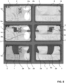
- Figure 5 illustrates that data carriers 1 can be manufactured that comprise target elements 2, 2a of arbitrary shapes and at arbitrary locations on and/or within the data carrier 1.
Landscapes
- Engineering & Computer Science (AREA)
- Manufacturing & Machinery (AREA)
- Physics & Mathematics (AREA)
- Health & Medical Sciences (AREA)
- Electromagnetism (AREA)
- General Health & Medical Sciences (AREA)
- Optics & Photonics (AREA)
- Toxicology (AREA)
- Credit Cards Or The Like (AREA)
Abstract
A method of producing a data carrier (1) comprising at least one target element (2) comprises the steps of i) arranging a processing layer (3) and a background layer (4) above one another, ii) irradiating electromagnetic radiation (R) onto the processing layer (3), wherein the processing layer (3) at regions of impingement of the electromagnetic radiation (R) is cut and sealed to the background layer (4), and iii) removing the processing layer (3) after the irradiation of the electromagnetic radiation (R), wherein a remaining part (5) of the processing layer (3) being sealed to the background layer (4) remains on the background layer (4), whereby the at least one target element (2) is formed.
Description
- The present invention relates to a method of producing a data carrier comprising a target element as claimed in
claim 1. - Data carrier of secure articles such as smart cards, banking cards, identity cards, drivers licences, passports or the like are well-known in the art. A common way to protect such data carriers against forgery is by means of elements being formed in the data carrier and which elements allow an authentication test. For instance, a transparent element or a translucent element can be formed in the data carrier and that can be controlled by a customer office. To this end it is common to introduce transparent or translucent elements into polycarbonate cards and data pages by using mostly transparent plastics, for instance in a so-called pick-and-place insert process. However, such a manufacturing is cumbersome and is associated with a low throughput and high costs.
- It is an object of the present invention to provide a method of producing a data carrier comprising at least one target element such as a transparent element or a translucent element that enables the production of the data carrier with high-throughput and at low costs.
- This object is achieved with a method according to
claim 1. That is, a method of producing a data carrier is provided, wherein the data carrier comprises at least one target element. The method comprises the steps of i) arranging a processing layer and a background layer above one another, ii) irradiating electromagnetic radiation onto the processing layer, wherein the processing layer at regions of impingement of the electromagnetic radiation is cut and sealed to the background layer, and iii) removing the processing layer after the irradiation of the electromagnetic radiation, wherein a remaining part of the processing layer being sealed to the background layer remains on the background layer, whereby the at least one target element is formed. - Steps i) to iii) are preferably consecutive steps.
- That is, the method according to the invention is based on the insight that a cutting process, in particular a laser cutting process, can be used to a) cut at least one part of the processing layer, and b) seal said cut part to the underlying background layer, and c) to allow for a part not being sealed to the processing layer to be removed from the processing layer. In this way a target element can be formed in the data carrier, wherein said target element is at least partially delimited or defined by the remaining part of the processing layer that remains sealed to the background layer.
- The target element preferably is at least partially delimited or defined by the remaining part of the processing layer and/or comprises or consists of at least part of the background layer. Additionally or alternatively, a shape of the target element preferably corresponds to a shape of a removable part of the processing layer that is removed from the background layer.
- As such, it is preferred that a cutting path or cutting trajectory of the electromagnetic radiation being irradiated onto the processing layer defines a desired shape or contour of the target element that is thus separated from the processing layer when the processing layer is removed from the background layer.
- In other words, the target element is preferably produced by generating a boundary element in the processing layer upon the irradiation of electromagnetic radiation from a source of electromagnetic radiation onto the processing layer, wherein the electromagnetic radiation cuts the processing layer and seals it to the background layer. In this way, a boundary element is formed in the processing layer, wherein the boundary element corresponds to a remaining part of the processing layer that is delimited by the cut and defined by the cutting path or cutting trajectory of the irradiated electromagnetic radiation. When the processing layer is removed, parts of the processing layer being outside of the boundary element are removed from the background layer, while said remaining part of the processing layer remains on the background layer. Hence, the boundary element can be seen as the remaining part of the processing layer that remains on the background layer.
- Consequently, the target element, in particular a shape of the target element, is preferably defined by a contour of the boundary element.
- Again in other words, the irradiation of electromagnetic radiation onto the processing layer can be seen as separating the processing layer into a removable part and the remaining part. Upon removal of the processing layer, the removable part of the processing layer being formed outside of the boundary element is removed from the background layer, leaving the remaining part of the processing layer on the background layer.
- As such, the target element can be seen as a part of the background layer from which the processing layer has been removed.
- The cutting trajectory or cutting path can be formed by moving the source of electromagnetic radiation with respect to the processing layer and the background layer. Additionally or alternatively, the cutting trajectory or cutting path can be formed by moving a direction along which the electromagnetic radiation is irradiated onto the processing layer. Additionally or alternatively, the cutting path or cutting trajectory can be formed by moving the processing layer and the background layer with respect to the source of electromagnetic radiation.
- It should be noted that a single target element can be formed. However, it is likewise conceivable that two or more target elements are formed. Explanations made herein regarding a target element preferably likewise apply to two or more target elements and vice versa.
- A shape and/or a location of the target element on the data carrier preferably is arbitrary.
- That is, since the electromagnetic radiation can be irradiated onto the processing layer arbitrarily, various cutting shapes at various locations on the processing layer can be generated. As such, a shape and/or location of the target element in the data carrier is arbitrary as well. For instance, the target element can be in edge regions of the data carrier or remote from the edge regions of the data carrier such as entirely within the data carrier. The target element can have the shape of an image and/or of an alphanumeric character, etc.
- The target element and/or the background layer are preferably at least partially transparent.
- That is, the method according to the invention allows the generation of so-called transparent elements, i.e. see-through elements such as window elements. These transparent elements can be surrounded by opaque material, can correspond to clear elements on edges of the data carrier, or can be any other geometrical combination of transparent and opaque parts, for instance.
- It is also possible to generate so-called translucent elements, e.g. when a target element in a direction perpendicular to a surface of the data carrier is followed by a layer that is non-transparent and which layer is not cut or otherwise removed. Such a translucent element can be formed by an uncut white layer, by an arbitrary cut in regions of a white material inside the just mentioned 'transparent elements' etc. Hence, the present invention allows the generation of translucent and/or transparent elements such as window elements according that is in a sense opposite to the methods known in the state of the art, i.e. the present invention allows the generation of opaque regions into a transparent body rather than transparent regions (windows) into an opaque body.
- That is, the present invention allows several applications: One is that clear edges or the like can be formed in the data carrier, wherein an additional window element is present or no window element is present at all. One is that there is a clear region and an opaque region arranged within the data carrier. For example, in the latter application a desired element could be the letter 'O' or a doughnut where the circular shape is transparent and both the outside and inside are opaque. In this case the clear region may be surrounded by an opaque region and thus be a window element, but it may also be located in an edge region of the data carrier.
- The background layer and/or the processing layer preferably comprise or consist of at least one polymer and/or plastics, preferably thermoplastics, particularly preferably polycarbonate and/or polyvinyl chloride and/or polyethylene terephthalate.
- That is, the background layer and/or the processing layer can comprise or consist of at least one polymer and/or plastics, in particular at least one thermoplastics. As mentioned initially, the background layer is preferably at least partially transparent. That is, the background layer can be partially transparent or entirely transparent. As such, it is preferred that the background layer comprises or consists of at least one polymer and/or plastics that is partially or entirely transparent. Examples of such partially or entirely transparent polymers and/or plastics are polycarbonate (PC), poly(ethylene terephthalate) (PET), polypropylene (PP) or polyethylene (PE), for instance.
- Additionally or alternatively, it is conceivable that the target element and/or the background layer are, at least in regions, opaque.
- The processing layer is preferably opaque. That is, the processing layer preferably comprises or consists of at least one polymer and/or plastics that is opaque. Examples of such opaque polymers and/or plastics polycarbonate (PC), poly(ethylene terephthalate) (PET), polypropylene (PP) or polyethylene (PE), for instance.
- That is, many options for the background layer and the processing layer are conceivable, wherein these layers taking different types of roles. For instance, the background layer could be at least partially or entirely transparent and the processing layer could be at least partially or entirely opaque. However, it is likewise conceivable that the background layer is opaque and that the processing layer adds a piece of different material or opaque such as differently coloured material etc. being visible from an outside of the data carrier and/or to cover one or more regions on the background layer in a translucent manner. For example, at least part of the processing layer could be provided as a protective element, for instance against light or some mechanical stress, or the combination could produce some desired effect.
- Additionally or alternatively, one or more pieces of the processing layer being cut could be arranged in the data carrier so as to provide an extra thickness to fill some void(s) in the layer structure during lamination of the data carrier, for instance. In this case it is preferred that both layers, i.e. the background layer and the processing layer, are transparent.
- That is to say, it is conceivable that the background layer and the processing layer have an opposite opacity and translucence, or one or both of these layers could be translucent in the sense that it has light transmittivity in at least some wave length range falling in between clear (e.g. plastic) and opaque (e.g. plastic; such as white), or that one or both of these layers have a surface treatment, for example a coating, that introduces further visual/optical functionalities. Again in other words, it is conceivable that the background layer and/or the processing layer comprise or consist of a clear or colored material, where the coloring may refer to a substrate characteristic or be the result of surface treatment. The coloring could be an optical characteristic in some wave length range, and/or the extent of coloring can range from 'tinted' translucent to opaque of some color.
- By way of illustration, it is conceivable that a window like element is produced, where at least some opaque layer is cut to have an opening and the cut and sealed piece produced in the method according to the invention is located at least partially overlapping this area to provide extra material during a lamination step to fill the opening. It is likewise conceivable in the case of coatings some material layer that is sensitive to material flow upon heating (e.g. lamination step) and it may be advantageous to provide such an element with a compensation layer, i.e. a layer of essentially similar thickness and with an opening for the more sensitive material to limit the material flow and deformation upon heating (lamination step).
- A thickness of the background layer with respect to an extension direction of the data carrier preferably is between 10 micrometer to 1000 micrometer, for instance between 10 micrometer to 500 micrometer, more preferably between 50 micrometer to 150 micrometer.
- A thickness of the processing layer with respect to an extension direction of the data carrier preferably is between 30 micrometer to 1000 micrometer, for instance between 30 micrometer to 100 micrometer such as about 50 micrometer.
- The extension direction of the data carrier preferably runs perpendicular to the transverse direction of the data carrier. In the final data carrier, the extension direction can be seen as a vertical direction and the transverse direction can be seen as a horizontal direction.
- The processing layer preferably is opaque. Additionally or alternatively, the remaining part of the processing layer is preferably configured to block, in particular visually block, at least part of the background layer towards an outside of the data carrier.
- That is, the remaining part of the processing layer is preferably configured to block, in particular visually block, at least part of the background layer towards an outside. In other words, the remaining part of the processing layer preferably covers or hides part of the background layer towards an outside of the data carrier such that said part of the background layer is not visible to an observer of the data carrier.
- Said visually blocking is preferably achieved by the opaque processing layer.
- Hence, and as mentioned earlier, the target element can be seen as a part of the background layer from which the processing layer has been removed. In other words, the target element preferably comprises or consists of a part of the background layer that is not blocked by the remaining opaque processing layer.
- The processing layer and the background layer are preferably arranged immediately above one another. Additionally or alternatively, the processing layer is preferably sealed to the background layer in the absence of any additional sealing element, in particular in the absence of any adhesive element.
- The processing layer and the background layer being arranged immediately above one another means that these layers are preferably in surface contact with one another. In fact, it is preferred that the processing layer is arranged above the background layer, and wherein a lower surface of the processing layer is in surface contact with an upper surface of the background layer.
- Moreover, a sealing of the processing layer to the background layer is preferably solely achieved by the irradiation of the electromagnetic radiation and a thus produced melting of the processing layer.
- In the final data carrier, the background layer preferably is a continuous layer and/or extends along an entire width of the data carrier when seen along a transverse direction of the data carrier. Additionally or alternatively, in the final data carrier, the remaining part of the processing layer preferably forms an intermittent processing layer when seen along the transverse direction of the data carrier.
- In the final data carrier, i.e. once the processing layer has been removed from the background layer, the background layer preferably is a continuous layer that lacks any recesses or holes or the like when seen along the transverse direction of the data carrier.
- Additionally or alternatively, the background layer preferably extends along an entire width of the final data carrier when seen along the transverse direction of the data carrier. That is, the background layer preferably extends all the way up to the edge regions of the data carrier.
- It should be noted that the final data carrier can comprise two or more processing layers and/or two or more background layers being arranged above one another with respect to the extension direction. Said layers can be alternatingly arranged, wherein a processing layer follows a background layer or vice versa, or said layers can be arranged non-alternatingly, wherein two processing layers are arranged above one another, for example.
- Moreover, said two or more processing layers and/or said two or more background layers can be the same or different from one another. For example, the final data carrier could comprise two processing layers being arranged above a background layer, wherein one of the processing layers covers a large area of the background layer leaving, for instance, just the edges of the data carrier clear and the other processing layer covers a smaller area of the background layer and serves the purpose of adding, for instance, a small piece of processing layer that comprises one or more additional elements or properties such as optical properties. In this case, the two processing layers are seen as being different from one another with respect to their areal extension, the presence of the window element(s) and of the optical properties. Other differences are of course likewise conceivable.
- Since parts of the processing layer are removed during the production of the data carrier while parts of the processing layer remain on the background layer upon removal of the processing layer from the background layer, the remaining parts of the processing layer can be seen in the final data carrier as an intermittent layer when seen along the transverse direction of the data carrier.
- The processing layer is preferably simultaneously cut and sealed to the background layer. Additionally or alternatively, the processing layer is preferably cut by ablation and/or the processing layer at the region of impingement of the electromagnetic radiation is preferably melted and thereby sealed to the background layer.
- That is, it is preferred that the irradiation of the electromagnetic radiation onto the processing layer simultaneously cuts and seals the processing layer in the region of the impingement of the electromagnetic radiation to the background layer.
- The electromagnetic radiation preferably is laser radiation. It is furthermore preferred that the irradiation of laser radiation results in an ablation, in particular in a laser ablation, of the processing layer at the region of impingement.
- To this end it is particularly preferred that the electromagnetic radiation only cuts, in particular ablates, only the processing layer, while it leaves the background layer intact.
- The cutting of the processing layer by the irradiation of the electromagnetic radiation can therefore be seen as kiss cutting, in particular laser kiss cutting the processing layer.
- Moreover, the irradiation of the laser radiation preferably melts the processing layer at the region of impingement and thereby seals the processing layer to the background layer. It is particularly preferred that the laser ablation and the melting take place simultaneously.
- Hence, in a sense, the production of the target element in the data carrier can be seen as generating a sealing effect of a laser in kiss cutting mode, wherein the laser cuts only the processing layer but not the background layer, while the heat of the laser seals the cutting edges of the processing layer onto the background layer. Then, when removing the processing layer, the sealed cutting edges break away from a "skeleton side" of the processing layer, leaving the cut element, i.e. the remaining part of the processing layer being delimited by the boundary element, attached onto the background layer.
- However, other technologies could be applied as well. For instance, US welding could be used instead of the above-described cutting and attaching, or punching and attaching by heat.
- The background layer and/or the processing layer are preferably provided in roll-form or sheet form. Additionally or alternatively, the background layer and/or the processing layer are preferably processed in a reel-to-reel process, in a sheet-to-sheet process or in a reel-to-sheet process.
- That is, the processing layer and/or the background layer are preferably provided in roll-form and are removed from the roll during the production of the data carrier. It is likewise preferred that the processing layer and/or the background layer are provided in sheet form.
- To this end various processing methods are conceivable. For instance, the background layer and/or the processing layer can be processed in a reel-to-reel process or in a sheet-to-sheet process or in a reel-to-sheet process as they are well-known in the art.
- In fact, any such process is conceivable as long as a cutting such as laser cutting can cut parts of the processing layer and seal at least these parts to the background layer such that the former can be removed/pulled off while the cut parts remain attached to the background layer.
- In any case, the processing layer and the background layer are preferably arranged above one another prior to an irradiation of the electromagnetic radiation. To this end it is particularly preferred that the processing layer is arranged above the background layer with respect to a processing direction, wherein the lower surface of the processing layer faces the upper surfaces of the background layer. Then, the electromagnetic radiation is preferably irradiated onto an upper surface of the processing layer being arranged opposite to the lower surface of the processing layer.
- During a reel-to-reel or reel-to-sheet or sheet-to-sheet process, wherein the processing layer and the background layer are arranged above one another, the processing layer and the background layer are preferably moved with respect to the source of electromagnetic radiation and thus the irradiation of the electromagnetic radiation from the source of electromagnetic radiation.
- Before and/or during and/or after the irradiation of electromagnetic radiation onto the processing layer, the processing layer and the background layer are preferably in surface contact with each other, particularly preferably because of a static force After the irradiation of the electromagnetic radiation, the processing layer is preferably removed from the background layer.
- The processing layer, after the irradiation of electromagnetic radiation, is preferably removed from the background layer by unwinding and/or in reel
- That is, after the irradiation of the electromagnetic radiation the processing layer can be unwound from the background layer, for instance in reel.
- Thereafter, it is preferred to singulate the background layer and the remaining part of the processing layer being arranged thereon in order to generate "units" of a desired size. The thus formed smaller units of the background layer and the remaining part of the processing layer preferably constitute a so-called inlay element or semi-finished element for a carrier body or card body as it is well-known in the field of the card industry, see also further below. To this end it is particularly preferred that the background layer and the remaining part of the processing layer being arranged thereon are singulated into a particular format being associated with an end-use of the data carrier.
- The background layer and the processing layer, preferably after the irradiation of the electromagnetic radiation and particularly preferably also after removing the processing layer from the background layer, are preferably singulated.
- The background layer and the remaining part of the processing layer, preferably after being singulated, are preferably incorporated into a carrier body. The carrier body preferably comprises or consists of one or more layers, the layers preferably comprising or consisting of at least one of a paper-based compound, a cardboard-based compound, a metallic compound, a plastics or a polymer.
- That is, it is preferred to incorporate such as laminate the background layer and the remaining part of the processing layer into a carrier body that comprises or consists of one or more layers.
- Said one or more layers of the carrier body preferably comprise or consist of polymers and/or plastics as mentioned earlier with respect to the background layer and the processing layer.
- Additionally or alternatively, the carrier body can comprise one or more layers comprising or consisting of one or more paper-based compounds and/or one or more cardboard-based compounds.
- The layers of the carrier body are preferably arranged above one another with respect to the extension direction and/or are preferably connected to one another by means commonly known in the state of the art. For instance, if the carrier body comprises two or more layers comprising or consisting of polymers and/or plastics, these layers could be connected to one another via lamination. However, other types of connection means are likewise conceivable. For instance, layers of a paper-based compound could be glued to one another.
- The carrier body preferably corresponds to a card body as it is known in the card industry.
- To this end it is particularly preferred that the background layer and the remaining part of the processing layer correspond to an inlay element or semi-finished element that is incorporated into the carrier body, in particular into the card body, by lamination.
- This state preferably provides the final data carrier.
- At least one further target element is preferably formed from at least one further processing layer. In the final data carrier, the target element and the further target element can be arranged congruent or at least partially offset with respect to one another when seen along an extension direction of the data carrier. In particular, the remaining parts of the processing layer and the remaining parts of the further processing layer can be arranged congruent or at least partially offset with respect to one another when seen along the extension direction of the data carrier. To this end it is preferred to arrange the processing layer on an upper surface of the background layer and the further processing layer on a lower surface of the background layer, wherein the target element is associated with the upper surface and the further target element is associated with the lower surface of the background layer. It is however also conceivable to provide at least one further background layer, and wherein the further processing layer is arranged on the further background layer.
- Depending on an arrangement of the target element with respect to the further target element, or of the background layer comprising the remaining part of the processing layer with respect to the further background layer comprising the remaining part of the further processing layer, different appearances or visual effects can be generated in the data carrier.
- The data carrier preferably is part of or constitutes a secure article, for instance a smart card, a banking card, an identity card, a drivers licence, a passport or the like.
- The data carrier being part of a secure article could be a data carrier integrated into a passport page of a passport.
- The data carrier constituting a secure article could be a data carrier in the form of a smart card, an identity card, a drivers licence, a banking card, etc.
- The data carrier or the secure article can comprise further components as they are known in the art. For instance, the data carrier and/or the secure article can comprise one or more security elements. Examples of security elements are an image and/or an alphanumeric character such as an image or name of the holder of the data carrier. Said security element can be provided in the form of a print, an embossing, debossing, an ablation, etc., as it is known in the field of the art.
- Preferred embodiments of the invention are described in the following with reference to the drawings, which are for the purpose of illustrating the present preferred embodiments of the invention and not for the purpose of limiting the same. In the drawings,
- Fig. 1
- shows a schematics of a method of producing a data carrier according to the invention;
- Fig. 2
- shows a cross-sectional view of a data carrier produced in the method according to the invention, wherein the data carrier comprises a target element;
- Fig. 3
- shows a photograph of a data carrier produced in the method according to the invention, wherein the data carrier comprises another target element;
- Fig. 4
- shows a photograph of a data carrier produced in the method according to the invention, wherein the data carrier comprises another target element;
- Fig. 5
- shows photographs of data carriers produced in the method according to the invention, wherein the data carriers comprises other target elements.
- Aspects of the present invention shall now be illustrated with reference to the figures.
- That is, the present invention concerns a method of producing a
data carrier 1 that comprises at least onetarget element 2. To this end aprocessing layer 3 is arranged immediately above abackground layer 4 in the absence of any sealing element, seefigure 1 . Thereafter, electromagnetic radiation R is irradiated onto theprocessing layer 3, wherein theprocessing layer 3 at regions of impingement of the electromagnetic radiation R is cut and sealed to thebackground layer 4. In fact, theprocessing layer 3 is simultaneously cut by ablation and melted and thereby sealed to thebackground layer 4 at the region of impingement of the electromagnetic radiation R. After the irradiation of the electromagnetic radiation, theprocessing layer 3 is removed from thebackground layer 4. A remainingpart 5 of theprocessing layer 3 being sealed to thebackground layer 4 remains on thebackground layer 4, whereby thetarget element 2 is formed. That is, thetarget element 2 can be seen as a part of thebackground layer 2 from which theprocessing layer 3 has been removed. In the depicted example, thebackground layer 4 and theprocessing layer 3 are both provided in roll-form and are processed in a reel-to-reel process. After the irradiation of electromagnetic radiation R, theprocessing layer 3 is removed from thebackground layer 4 by unwinding and in reel. - As follows from
figure 1 , thetarget element 2 is at least partially delimited or defined by the remainingpart 5 of theprocessing layer 3, wherein a shape of thetarget element 2 corresponds to a shape of aremovable part 6 of theprocessing layer 3 that is removed from thebackground layer 4. - The
background layer 4 and the remainingpart 5 of theprocessing layer 3 correspond here to an inlay element or semi-finished element that is incorporated into acarrier body 7 of thedata carrier 1, seefigure 2 . As furthermore follows fromfigure 2 , thecarrier body 7 comprises several layers that are arranged above one another with respect to an extension direction E of thedata carrier 1. In the example depicted infigure 2 , thecarrier body 7 comprises remainingparts processing layers upper surface 8 and on alower surface 9 of thebackground layer 4. That is, thedata carrier 1 comprises afirst target element 2 being associated with theupper surface 8 of thebackground layer 4 and asecond target element 2a being associated with thelower surface 9 of thebackground layer 4. Thecarrier body 7 furthermore comprises atop layer 10 being arranged on the remainingpart 5 of theupper processing layer 3 and abottom layer 11 being arranged on the remainingpart 5a of the lower processing layer 3a. Saidtop layer 10 andbottom layer 11 constitute atop side 12 and abottom side 13 of thedata carrier 1, respectively. In thisfinal data carrier 1, thebackground layer 4 is a continuous layer that extends along an entire width of thedata carrier 1 when seen along a transverse direction T of thedata carrier 1 running perpendicularly to the extension direction E of thedata carrier 1. The remainingparts data carrier 1. - In the depicted examples, the
background layer 4 is transparent and the processing layers 3, 3a are opaque. - In the event that the remaining
parts parts target elements parts - As such, the method according to the invention allows the formation of a single opaque such as white element within a translucent structure such that a floating effect is created. However, many other designs and arrangements of the
target elements figure 3 illustrates adata carrier 1 that comprises atarget element 2 in the form ofclear edge regions 14 of the data carrier.Figure 4 illustrates adata carrier 1 comprisingtarget elements clear edge regions 14 as well as a transparent window element being arranged within the data carrier.Figure 5 illustrates thatdata carriers 1 can be manufactured that comprisetarget elements data carrier 1.LIST OF REFERENCE SIGNS 1 data carrier 9 lower surface 2, 2a target element 10 top layer 3, 3a processing layer 11 bottom layer 4 background layer 12 top side 5 remaining part of processing layer 13 bottom side 14 edge region 6 removable part of processing layer R electromagnetic radiation 7 carrier body E extension direction 8 upper surface T transverse direction
Claims (15)
- A method of producing a data carrier (1),wherein the data carrier (1) comprises at least one target element (2),
andwherein the method comprises the steps of:- Arranging a processing layer (3) and a background layer (4) above one another;- Irradiating electromagnetic radiation (R) onto the processing layer (3), wherein the processing layer (3) at regions of impingement of the electromagnetic radiation (R) is cut and sealed to the background layer (4); and- Removing the processing layer (3) after the irradiation of the electromagnetic radiation (R), wherein a remaining part (5) of the processing layer (3) being sealed to the background layer (4) remains on the background layer (4), whereby the at least one target element (2) is formed. - The method according to claim 1, wherein the target element (2) is at least partially delimited or defined by the remaining part (5) of the processing layer (3) and/or comprises or consists of at least part of the background layer (4), and/or
wherein a shape of the target element (2) corresponds to a shape of a removable part (6) of the processing layer (3) that is removed from the background layer (4). - The method according to any one of the preceding claims, wherein a shape and/or a location of the target element (2) on the data carrier (1) is arbitrary.
- The method according to any one of the preceding claims, wherein the target element (2) and/or the background layer (4) are at least partially transparent, and/or
wherein the target element (2) and/or the background layer (4) are at least in regions opaque. - The method according to any one of the preceding claims, wherein the background layer (4) and/or the processing layer (3) comprises or consists of at least one polymer and/or plastics, preferably thermoplastics, particularly preferably polycarbonate and/or polyvinyl chloride and/or polyethylene terephthalate.
- The method according to any one of the preceding claims, wherein the processing layer (3) is opaque, and/or
wherein the remaining part (5) of the processing layer (3) is configured to block, in particular visually block, at least part of the background layer (4) towards an outside of the data carrier (1). - The method according to any one of the preceding claims, wherein the processing layer (3) and the background layer (4) are arranged immediately above one another, and/or
wherein the processing layer (3) is sealed to the background layer (4) in the absence of any additional sealing element, in particular in the absence of any adhesive element. - The method according to any one of the preceding claims, wherein, in the final data carrier (1), the background layer (4) is a continuous layer and/or extends along an entire width of the data carrier (1) when seen along a transverse direction (T) of the data carrier (1), and/or
wherein, in the final data carrier (1), the remaining part (5) of the processing layer (3) forms an intermittent processing layer (3) when seen along the transverse direction (T) of the data carrier (1). - The method according to any one of the preceding claims, wherein the processing layer (3) is simultaneously cut and sealed to the background layer (4), and/or
wherein at least one of the processing layer (3) is cut by ablation and the processing layer (3) at the region of impingement of the electromagnetic radiation (R) is melted and thereby sealed to the background layer (4). - The method according to any one of the preceding claims, wherein the background layer (4) and/or the processing layer (3) are provided in roll-form or sheet form and/or are processed in a reel-to-reel process, in a sheet-to-sheet process or in a reel-to-sheet process.
- The method according to claim 10, wherein the processing layer (3), after the irradiation of electromagnetic radiation (R), is removed from the background layer (4) by unwinding and/or in reel.
- The method according to any one of the preceding claims, wherein the background layer (4) and the processing layer (3), preferably after the irradiation of the electromagnetic radiation (R) and particularly preferably also after removing the processing layer (3) from the background layer (4), are singulated.
- The method according to any one of the preceding claims, wherein the background layer (4) and the remaining part (5) of the processing layer (3), preferably after being singulated, are incorporated into a carrier body (7), and
wherein the carrier body (7) preferably comprises or consists of one or more layers, the layers preferably comprising or consisting of at least one of a paper-based compound, a cardboard-based compound, a metallic compound, a plastics or a polymer. - The method according to any one of the preceding claims, wherein at least one further target element (2a) is formed from at least one further processing layer (3a), and
wherein, in the final data carrier (1), the target element (2) and the further target element (2a) are arranged congruent or at least partially offset with respect to one another when seen along an extension direction (E) of the data carrier (1). - The method according to any one of the preceding claims, wherein the data carrier (1) is part of or constitutes a secure article, for instance a smart card, a banking card, an identity card, a drivers licence, a passport or the like.
Priority Applications (4)
| Application Number | Priority Date | Filing Date | Title |
|---|---|---|---|
| EP23307369.1A EP4574443A1 (en) | 2023-12-22 | 2023-12-22 | Data carrier with clear effects |
| PCT/EP2024/088269 WO2025133365A1 (en) | 2023-12-22 | 2024-12-20 | Data carrier with clear effects |
| AU2024404775A AU2024404775A1 (en) | 2023-12-22 | 2024-12-20 | Data carrier with clear effects |
| CN202480079903.5A CN122497592A (en) | 2023-12-22 | 2024-12-20 | Data carrier with clear effect |
Applications Claiming Priority (1)
| Application Number | Priority Date | Filing Date | Title |
|---|---|---|---|
| EP23307369.1A EP4574443A1 (en) | 2023-12-22 | 2023-12-22 | Data carrier with clear effects |
Publications (1)
| Publication Number | Publication Date |
|---|---|
| EP4574443A1 true EP4574443A1 (en) | 2025-06-25 |
Family
ID=90053618
Family Applications (1)
| Application Number | Title | Priority Date | Filing Date |
|---|---|---|---|
| EP23307369.1A Withdrawn EP4574443A1 (en) | 2023-12-22 | 2023-12-22 | Data carrier with clear effects |
Country Status (4)
| Country | Link |
|---|---|
| EP (1) | EP4574443A1 (en) |
| CN (1) | CN122497592A (en) |
| AU (1) | AU2024404775A1 (en) |
| WO (1) | WO2025133365A1 (en) |
Citations (2)
| Publication number | Priority date | Publication date | Assignee | Title |
|---|---|---|---|---|
| US20200114677A1 (en) * | 2018-10-16 | 2020-04-16 | Idemia Identity & Security USA LLC | Fused polyester identification documents |
| EP4177066A1 (en) * | 2021-11-09 | 2023-05-10 | Thales Dis France SAS | Data carriers and methods of producing them |
-
2023
- 2023-12-22 EP EP23307369.1A patent/EP4574443A1/en not_active Withdrawn
-
2024
- 2024-12-20 CN CN202480079903.5A patent/CN122497592A/en active Pending
- 2024-12-20 WO PCT/EP2024/088269 patent/WO2025133365A1/en active Pending
- 2024-12-20 AU AU2024404775A patent/AU2024404775A1/en active Pending
Patent Citations (2)
| Publication number | Priority date | Publication date | Assignee | Title |
|---|---|---|---|---|
| US20200114677A1 (en) * | 2018-10-16 | 2020-04-16 | Idemia Identity & Security USA LLC | Fused polyester identification documents |
| EP4177066A1 (en) * | 2021-11-09 | 2023-05-10 | Thales Dis France SAS | Data carriers and methods of producing them |
Also Published As
| Publication number | Publication date |
|---|---|
| WO2025133365A1 (en) | 2025-06-26 |
| CN122497592A (en) | 2026-07-31 |
| AU2024404775A1 (en) | 2026-06-18 |
Similar Documents
| Publication | Publication Date | Title |
|---|---|---|
| DK2756963T3 (en) | PROCEDURE FOR MANUFACTURING A MULTIPLE LAYER DATA AND A DATA SHEET MADE USING THIS PROCEDURE | |
| US20110204617A1 (en) | Security article and method of manufacture | |
| DE3268726D1 (en) | Flat card of thermoplastic material with visually readable security marks, and process for manufacturing the same | |
| EP3359391B1 (en) | A security sheet for an identity document | |
| KR20010024592A (en) | Method and apparatus for the automatic production of personalized cards and pouches | |
| KR101230122B1 (en) | Valuable document and method for producing a valuable document | |
| EP3463924A1 (en) | Sheet of paper for a security document, method for producing the sheet of paper, and security document produced therewith | |
| EP2081775B1 (en) | Method for producing a data carrier and data carrier produced therefrom | |
| WO2025133365A1 (en) | Data carrier with clear effects | |
| CN113195240A (en) | Method for producing a film intermediate product, film intermediate product and method for producing a product | |
| CA2368056C (en) | Data carrier and method for producing same | |
| GB2269340A (en) | Security card produced as continuous stationery | |
| EP4303027B1 (en) | Valuable or security product and method for the production thereof | |
| EP3892473A1 (en) | Data carrier with protection against subsequent laser marking | |
| DE102017012496B4 (en) | security document and process for its production | |
| DE102017117271B4 (en) | Security document and method of making it | |
| NZ707967B2 (en) | Method for producing a multilayer data carrier and data carrier produced by said method |
Legal Events
| Date | Code | Title | Description |
|---|---|---|---|
| PUAI | Public reference made under article 153(3) epc to a published international application that has entered the european phase |
Free format text: ORIGINAL CODE: 0009012 |
|
| STAA | Information on the status of an ep patent application or granted ep patent |
Free format text: STATUS: THE APPLICATION HAS BEEN PUBLISHED |
|
| AK | Designated contracting states |
Kind code of ref document: A1 Designated state(s): AL AT BE BG CH CY CZ DE DK EE ES FI FR GB GR HR HU IE IS IT LI LT LU LV MC ME MK MT NL NO PL PT RO RS SE SI SK SM TR |
|
| STAA | Information on the status of an ep patent application or granted ep patent |
Free format text: STATUS: THE APPLICATION IS DEEMED TO BE WITHDRAWN |
|
| 18D | Application deemed to be withdrawn |
Effective date: 20260103 |