EP4572562A1 - Power semiconductor device and power converter including the same - Google Patents
Power semiconductor device and power converter including the same Download PDFInfo
- Publication number
- EP4572562A1 EP4572562A1 EP24219704.4A EP24219704A EP4572562A1 EP 4572562 A1 EP4572562 A1 EP 4572562A1 EP 24219704 A EP24219704 A EP 24219704A EP 4572562 A1 EP4572562 A1 EP 4572562A1
- Authority
- EP
- European Patent Office
- Prior art keywords
- conductivity type
- power semiconductor
- well
- semiconductor device
- wells
- Prior art date
- Legal status (The legal status is an assumption and is not a legal conclusion. Google has not performed a legal analysis and makes no representation as to the accuracy of the status listed.)
- Pending
Links
Images




Classifications
-
- H—ELECTRICITY
- H10—SEMICONDUCTOR DEVICES; ELECTRIC SOLID-STATE DEVICES NOT OTHERWISE PROVIDED FOR
- H10D—INORGANIC ELECTRIC SEMICONDUCTOR DEVICES
- H10D62/00—Semiconductor bodies, or regions thereof, of devices having potential barriers
- H10D62/10—Shapes, relative sizes or dispositions of the regions of the semiconductor bodies; Shapes of the semiconductor bodies
- H10D62/102—Constructional design considerations for preventing surface leakage or controlling electric field concentration
- H10D62/103—Constructional design considerations for preventing surface leakage or controlling electric field concentration for increasing or controlling the breakdown voltage of reverse-biased devices
- H10D62/105—Constructional design considerations for preventing surface leakage or controlling electric field concentration for increasing or controlling the breakdown voltage of reverse-biased devices by having particular doping profiles, shapes or arrangements of PN junctions; by having supplementary regions, e.g. junction termination extension [JTE]
- H10D62/106—Constructional design considerations for preventing surface leakage or controlling electric field concentration for increasing or controlling the breakdown voltage of reverse-biased devices by having particular doping profiles, shapes or arrangements of PN junctions; by having supplementary regions, e.g. junction termination extension [JTE] having supplementary regions doped oppositely to or in rectifying contact with regions of the semiconductor bodies, e.g. guard rings with PN or Schottky junctions
- H10D62/107—Buried supplementary regions, e.g. buried guard rings
-
- H—ELECTRICITY
- H02—GENERATION; CONVERSION OR DISTRIBUTION OF ELECTRIC POWER
- H02M—APPARATUS FOR CONVERSION BETWEEN AC AND AC, BETWEEN AC AND DC, OR BETWEEN DC AND DC, AND FOR USE WITH MAINS OR SIMILAR POWER SUPPLY SYSTEMS; CONVERSION OF DC OR AC INPUT POWER INTO SURGE OUTPUT POWER; CONTROL OR REGULATION THEREOF
- H02M7/00—Conversion of AC power input into DC power output; Conversion of DC power input into AC power output
- H02M7/42—Conversion of DC power input into AC power output without possibility of reversal
- H02M7/44—Conversion of DC power input into AC power output without possibility of reversal by static converters
- H02M7/48—Conversion of DC power input into AC power output without possibility of reversal by static converters using discharge tubes with control electrode or semiconductor devices with control electrode
- H02M7/53—Conversion of DC power input into AC power output without possibility of reversal by static converters using discharge tubes with control electrode or semiconductor devices with control electrode using devices of a triode or transistor type requiring continuous application of a control signal
- H02M7/537—Conversion of DC power input into AC power output without possibility of reversal by static converters using discharge tubes with control electrode or semiconductor devices with control electrode using devices of a triode or transistor type requiring continuous application of a control signal using semiconductor devices only, e.g. single switched pulse inverters
- H02M7/5387—Conversion of DC power input into AC power output without possibility of reversal by static converters using discharge tubes with control electrode or semiconductor devices with control electrode using devices of a triode or transistor type requiring continuous application of a control signal using semiconductor devices only, e.g. single switched pulse inverters in a bridge configuration
-
- H—ELECTRICITY
- H02—GENERATION; CONVERSION OR DISTRIBUTION OF ELECTRIC POWER
- H02P—CONTROL OR REGULATION OF ELECTRIC MOTORS, ELECTRIC GENERATORS OR DYNAMO-ELECTRIC CONVERTERS; CONTROLLING TRANSFORMERS, REACTORS OR CHOKE COILS
- H02P27/00—Arrangements or methods for the control of AC motors characterised by the kind of supply voltage
- H02P27/04—Arrangements or methods for the control of AC motors characterised by the kind of supply voltage using variable-frequency supply voltage, e.g. inverter or converter supply voltage
- H02P27/06—Arrangements or methods for the control of AC motors characterised by the kind of supply voltage using variable-frequency supply voltage, e.g. inverter or converter supply voltage using DC to AC converters or inverters
-
- H—ELECTRICITY
- H10—SEMICONDUCTOR DEVICES; ELECTRIC SOLID-STATE DEVICES NOT OTHERWISE PROVIDED FOR
- H10D—INORGANIC ELECTRIC SEMICONDUCTOR DEVICES
- H10D30/00—Field-effect transistors [FET]
- H10D30/01—Manufacture or treatment
- H10D30/021—Manufacture or treatment of FETs having insulated gates [IGFET]
- H10D30/028—Manufacture or treatment of FETs having insulated gates [IGFET] of double-diffused metal oxide semiconductor [DMOS] FETs
- H10D30/0291—Manufacture or treatment of FETs having insulated gates [IGFET] of double-diffused metal oxide semiconductor [DMOS] FETs of vertical DMOS [VDMOS] FETs
- H10D30/0297—Manufacture or treatment of FETs having insulated gates [IGFET] of double-diffused metal oxide semiconductor [DMOS] FETs of vertical DMOS [VDMOS] FETs using recessing of the gate electrodes, e.g. to form trench gate electrodes
-
- H—ELECTRICITY
- H10—SEMICONDUCTOR DEVICES; ELECTRIC SOLID-STATE DEVICES NOT OTHERWISE PROVIDED FOR
- H10D—INORGANIC ELECTRIC SEMICONDUCTOR DEVICES
- H10D30/00—Field-effect transistors [FET]
- H10D30/60—Insulated-gate field-effect transistors [IGFET]
- H10D30/64—Double-diffused metal-oxide semiconductor [DMOS] FETs
- H10D30/65—Lateral DMOS [LDMOS] FETs
-
- H—ELECTRICITY
- H10—SEMICONDUCTOR DEVICES; ELECTRIC SOLID-STATE DEVICES NOT OTHERWISE PROVIDED FOR
- H10D—INORGANIC ELECTRIC SEMICONDUCTOR DEVICES
- H10D30/00—Field-effect transistors [FET]
- H10D30/60—Insulated-gate field-effect transistors [IGFET]
- H10D30/64—Double-diffused metal-oxide semiconductor [DMOS] FETs
- H10D30/66—Vertical DMOS [VDMOS] FETs
-
- H—ELECTRICITY
- H10—SEMICONDUCTOR DEVICES; ELECTRIC SOLID-STATE DEVICES NOT OTHERWISE PROVIDED FOR
- H10D—INORGANIC ELECTRIC SEMICONDUCTOR DEVICES
- H10D30/00—Field-effect transistors [FET]
- H10D30/60—Insulated-gate field-effect transistors [IGFET]
- H10D30/64—Double-diffused metal-oxide semiconductor [DMOS] FETs
- H10D30/66—Vertical DMOS [VDMOS] FETs
- H10D30/668—Vertical DMOS [VDMOS] FETs having trench gate electrodes, e.g. UMOS transistors
-
- H—ELECTRICITY
- H10—SEMICONDUCTOR DEVICES; ELECTRIC SOLID-STATE DEVICES NOT OTHERWISE PROVIDED FOR
- H10D—INORGANIC ELECTRIC SEMICONDUCTOR DEVICES
- H10D62/00—Semiconductor bodies, or regions thereof, of devices having potential barriers
- H10D62/10—Shapes, relative sizes or dispositions of the regions of the semiconductor bodies; Shapes of the semiconductor bodies
- H10D62/124—Shapes, relative sizes or dispositions of the regions of semiconductor bodies or of junctions between the regions
- H10D62/126—Top-view geometrical layouts of the regions or the junctions
- H10D62/127—Top-view geometrical layouts of the regions or the junctions of cellular field-effect devices, e.g. multicellular DMOS transistors or IGBTs
-
- H—ELECTRICITY
- H10—SEMICONDUCTOR DEVICES; ELECTRIC SOLID-STATE DEVICES NOT OTHERWISE PROVIDED FOR
- H10D—INORGANIC ELECTRIC SEMICONDUCTOR DEVICES
- H10D62/00—Semiconductor bodies, or regions thereof, of devices having potential barriers
- H10D62/10—Shapes, relative sizes or dispositions of the regions of the semiconductor bodies; Shapes of the semiconductor bodies
- H10D62/13—Semiconductor regions connected to electrodes carrying current to be rectified, amplified or switched, e.g. source or drain regions
- H10D62/149—Source or drain regions of field-effect devices
- H10D62/151—Source or drain regions of field-effect devices of IGFETs
- H10D62/156—Drain regions of DMOS transistors
- H10D62/157—Impurity concentrations or distributions
-
- H—ELECTRICITY
- H10—SEMICONDUCTOR DEVICES; ELECTRIC SOLID-STATE DEVICES NOT OTHERWISE PROVIDED FOR
- H10D—INORGANIC ELECTRIC SEMICONDUCTOR DEVICES
- H10D62/00—Semiconductor bodies, or regions thereof, of devices having potential barriers
- H10D62/80—Semiconductor bodies, or regions thereof, of devices having potential barriers characterised by the materials
- H10D62/83—Semiconductor bodies, or regions thereof, of devices having potential barriers characterised by the materials being Group IV materials, e.g. B-doped Si or undoped Ge
- H10D62/832—Semiconductor bodies, or regions thereof, of devices having potential barriers characterised by the materials being Group IV materials, e.g. B-doped Si or undoped Ge being Group IV materials comprising two or more elements, e.g. SiGe
- H10D62/8325—Silicon carbide
Definitions
- the embodiment relates to a power semiconductor device, a power semiconductor module, a power converter, and a method of manufacturing the same.
- Power semiconductors are one of the key elements that determine the efficiency, speed, durability, and reliability of power electronic systems.
- WBG wide bandgap
- SiC silicon carbide
- GaN gallium nitride
- WBG power semiconductor devices have a band gap energy that is approximately three times that of Si power semiconductor devices. Due to this, WBG power semiconductor device has the characteristics of low intrinsic carrier concentration, high breakdown electric field (about 4 to 20 times), high thermal conductivity (about 3 to 13 times), and large electron saturation rate (about 2 to 2.5 times).
- gallium nitride (GaN) power semiconductor devices can be used in low-voltage systems
- silicon carbide (SiC) power semiconductor devices can be suitable for high-voltage systems.
- SiC MOSFET power semiconductors of the prior art are generally denoted as VDMOSFET with a vertical diffused structure, and may also be simply denoted as double-diffused structure DMOSFET. Additionally, SiC MOSFET can be classified into Planar MOSFET and Trench MOSFET depending on the direction of the channel.
- Trench MOSFET is a structure in which a channel is formed on the sidewall of the trench.
- a gate insulating film is formed on the sidewall of the trench and a gate electrode is formed in the trench.
- Trench MOSFET has the advantage of increasing channel density by forming channels on the sidewalls of the trench.
- the trench MOSFET has a larger electric field in the trench gate oxide, which has a shorter drift distance than the P-base (P-well).
- the electric field is concentrated at the trench edge of the trench, there is a problem that gate oxide breakdown occurs quickly and the breakdown voltage (BV) decreases.
- the breakdown field strength is 10 times that of silicon (Si), so SiC semiconductor devices are used with a voltage close to 10 times that of Si devices. For this reason, an electric field 10 times stronger than that of the silicon device is applied to the gate insulating film formed in the trench, causing a problem in which the gate insulating film is easily destroyed at the corners of the trench.
- One of the technical objects of the embodiment is to solve the technical contradiction of preventing breakdown voltage drop and increasing on-resistance (R on ) due to preventing electric field concentration at the corner of the trench.
- the embodiment is intended to prevent the On-resistance from increasing while preventing electric field concentration in the bottom P-well at the corner of the trench.
- a power semiconductor device includes a substrate, a first epitaxial (“epi") layer of a first conductivity type disposed on the substrate, a second epi layer of the first conductivity type disposed on the first epi layer of first conductivity type, first wells of the second conductivity type spaced apart from each other and disposed on or in the second epi layer of the first conductivity type, a third well of the second conductivity type disposed in the second epi layer of the first conductivity type and below the spaced apart first wells of the second conductivity type and an ion implantation connection region of the second conductivity type configured to connect the first wells of the second conductivity type to the third well of the second conductivity type.
- epi epitaxial
- a power semiconductor device includes a substrate 110, a first epi layer 111 of a first conductivity type disposed on the substrate 110, and a second epi layer 112 of the first conductivity type disposed on the first epi layer 111 of the first conductivity type, and first wells 121 of a second conductivity type spaced apart from each other and disposed on or in the second epi layer 112 of the first conductivity type.
- the power semiconductor device may further include a source region of the first conductivity type 141 disposed on at least one of the first wells 121 of the second conductivity type.
- the power semiconductor device may further include a second gate insulating layer 131b disposed on at least one of the source region of the first conductivity type 141, and said at least one of the first wells 121 of the second conductivity type and the second epi layer 112 of the first conductivity type, and a second gate 132b disposed on the second gate insulating layer 131b.
- the power semiconductor device may include a third well 124b of the second conductivity type disposed in or on the second epi layer 112 of the first conductivity type below the spaced apart first wells 121 of the second conductivity type (and/or on a lower side between the spaced apart first wells 121 of the second conductivity type).
- the power semiconductor device may include a ion implantation connection region 126 of the second conductivity type connecting the first wells 121 of the second conductivity type and the third well 124b of the second conductivity type.
- a ground potential When a ground potential is applied to the first wells 121 of the second conductivity type, a ground potential may also be applied to the third well 124b of the second conductivity type is formed by the ion implantation connection region 126 of the second conductivity type.
- a horizontal width of the third well 124b of the second conductivity type may be greater than or equal to a distance between the first wells 121 of the second conductivity type.
- the third well 124b of the second conductivity type may be disposed below a region between the spaced apart first wells 121 of the second conductivity type.
- the second gate may be disposed in a continuous form along a region of second gate.
- the third well 124b of the second conductivity type may be arranged in a continuous form along the second gate.
- the third well 124b of the second conductivity type may be arranged to extend (e.g. horizontally) in a first direction (Y), which is the direction in which the second gate 132b extends.
- the ion implantation connection region 126 of the second conductivity type may be arranged to extend in a second direction (X) perpendicular to the first direction (Y).
- the ion implantation connection region 126 of the second conductivity type may be arranged to extend in the second direction (X) perpendicular to the first direction (Y) while connecting the third well 124b of the second conductivity type disposed horizontally in the first direction (Y) while being spaced apart in the first direction (Y).
- the ion implantation connection region 126 of the second conductivity type may include a first ion implantation connection region 126a of the second conductivity type connecting the third well 124b of the second conductivity type disposed below the second gate 132b of a first cell region to the third well 124b of the second conductivity type disposed below the second gate 132b of a third cell region adjacent in the positive direction of said first cell region.
- a cell region may denote a region which includes a gate, a source region and a drain region.
- the third cell region may be disposed adjacent at a left side of the first cell region.
- a second cell region may be disposed adjacent at a right side of the first cell region.
- a fourth cell region may be disposed adjacent at a right side of the second cell region.
- the third well of the second conductivity type may include a third-first well of the second conductivity type disposed below the second gate of a first cell region, and a third-second well of the second conductivity type disposed below the second gate of a third cell region adjacent to a positive X-axis direction of the first cell region.
- the ion implantation connection region of the second conductivity type may include a first ion implantation connection region of the second conductivity type connecting the third-first well of second conductivity type to the third-second well of the second conductivity type.
- a ground potential When a ground potential is applied to the first wells of the second conductivity type, a ground potential may also be applied to the third well of the second conductivity type by the ion implantation connection region of the second conductivity type.
- a horizontal width of the third-first well of the second conductivity type may be greater than or equal to a distance between the first wells of the second conductivity type.
- the first ion implantation connection region 126a of the second conductivity type may connect the third well 124b of the second conductivity type of the first cell region and the third well 124b of the second conductivity type of the third cell region to the first wells 121 of the second conductivity type on the upper side.
- the ion implantation connection region 126 of the second conductivity type may include a second ion implantation connection region 126b of the second conductivity type connecting the third well 124b of the second conductivity type disposed below the second gate 132b of the second cell region to the third well 124b of the second conductivity type disposed below the second gate 132b of the fourth cell region adjacent in the negative (-) direction of the X-axis of second cell region.
- the second ion implantation connection region 126b of the second conductivity type may connect the third well 124b of the second conductivity type of second cell region and third well 124b of the second conductivity type well of the fourth cell region to the first wells 121 of the second conductivity type on the upper side.
- a power converter may include any of the above described power semiconductor devices.
- the power converter including the same, and the manufacturing method of the power semiconductor device according to the embodiment, there is a technical effect that it can solve the problem of increasing on-resistance (R on ) while preventing electric field concentration at the trench corner or the problem that adversely affect the electrical characteristics of the power semiconductor device.
- R on on-resistance
- the second well 124 of second conductivity type is disposed on the bottom side of the trench, and is disposed in a continuous form along the trench area, there is a technical effect of dispersing the electric field concentrated at the corner of the trench, preventing the breakdown voltage drop of the gate insulating layer, and improving the reliability of the gate insulating layer.
- the ion implantation connection region 126 of second conductivity type may connect the second well 124 of second conductivity type and the first wells 121 of second conductivity type. Accordingly, the first wells 121 of second conductivity type to which the ground potential is applied is connected to the second well 124 of second conductivity type by the ion implantation connection region 126 of second conductivity type, allowing the second well 124 of second conductivity type to also be at ground potential.
- the second well 124 of second conductivity type does not directly contact the bottom of the gate trench, there is an advantage in terms of thickness and characteristics that there is a reduced risk of forming an unexpectedly grown oxide layer during the thermal oxidation process for forming the gate insulating layer.
- the first wells 121 of second conductivity type to which the ground potential is applied is connected to the third well 124b of second conductivity type by the ion implantation connection region 126 of second conductivity type. Accordingly, the ground potential may also be applied to the third well 124b of second conductivity type. Therefore, there is a complex technical effect of preventing an increase in on-resistance (Ron) by applying the ground potential to the third well 124b of second conductivity type, which prevents electric field concentration.
- Ron on-resistance
- the first ion implantation connection region 126a of second conductivity type or the second ion implantation connection region 126b of second conductivity type can be disposed only on one side or the other side below the second gate 132b of each cell, there is a complex technical effect that can improve current flow.
- module and “unit” for the elements used in the following description are simply given in consideration of ease of writing this specification, and do not themselves give a particularly important meaning or role. Accordingly, the “module” and “unit” can be used interchangeably.
- FIG. 1 is a circuit diagram of a power converter 1000 according to an embodiment.
- the power converter 1000 according to the embodiment can receive DC power from a battery or fuel cell, convert it into AC power, and supply AC power to a predetermined load.
- the power converter 1000 according to the embodiment can include an inverter, which receive DC power from a battery, convert DC power into 3-phase AC power, and supply 3-phase AC power to a motor M.
- motor M can provide power to electric vehicles or fuel cell vehicles.
- the power converter 1000 can include the power semiconductor device 100.
- the power semiconductor device 100 can be a Metal Oxide Semiconductor Field Effect Transistor (MOSFET), but is not limited thereto, and can include an Insulated Gate Bipolar Transistor (IGBT).
- MOSFET Metal Oxide Semiconductor Field Effect Transistor
- IGBT Insulated Gate Bipolar Transistor
- the power converter 1000 can include a plurality of power semiconductor devices 100a, 100b, 100c, 100d, 100e, and 100f, and can include a plurality of diodes (not shown).
- Each of the plurality of diodes can be internally incorporated in each of the power semiconductor devices 100a, 100b, 100c, 100d, 100e, and 100f in the form of an internal diode, but is not limited thereto, and can be disposed separately.
- DC power can be converted into AC power through on-off control of the plurality of power semiconductor devices 100a to 100f.
- the first power semiconductor device 100a can be turned on and the second power semiconductor device 100b can be turned off in a first time period of one cycle to supply positive polarity power to the motor M.
- the first power semiconductor device 100a can be turned off and the second power semiconductor device 100b can be turned on to supply negative polarity power to the motor M.
- a group of power semiconductor devices disposed in series in a high voltage line and a low voltage line of an input side can be referred to as an arm.
- the first power semiconductor device 100a and the second power semiconductor device 100b can constitute a first arm
- the third power semiconductor device 100c and the fourth power semiconductor device 100d can constitute a second arm
- the fifth power semiconductor device 100e and the sixth power semiconductor device 100f can constitute a third arm.
- an upper side power semiconductor device and a bottom side power semiconductor device can be controlled not to turn on at the same time.
- the first power semiconductor device 100a and the second power semiconductor device 100b do not simultaneously turn on, but can turn on and off alternately.
- Each of the power semiconductor devices 100a to 100f can receive high power in an off state.
- the input voltage can be applied to the second power semiconductor device 100b as it is.
- the voltage input to the second power semiconductor device 100b can be a relatively high voltage, and a withstand voltage of each power semiconductor device 100a to 100f can be designed to have a high level to withstand such a high voltage.
- Each of the power semiconductor devices 100a to 100f can conduct a high current in a turn on state.
- the motor M can be driven with a relatively high current, and this high current can be supplied to the motor M through a power semiconductor device that is turned on.
- a high voltage applied to each of the power semiconductor devices 100a to 100f can cause a high switching loss.
- a high current conducting the power semiconductor devices 100a to 100f can cause a high conduction loss.
- the power semiconductor devices 100a to 100f can be packaged as a power semiconductor module including a heat dissipation means.
- the power semiconductor device 100 of the embodiment can be a silicon carbide (SiC) power semiconductor device, can operate in a high-temperature, high-voltage environment, and can have a high switching speed and low switching loss.
- SiC silicon carbide
- the power converter 1000 can include a plurality of power semiconductor modules.
- the plurality of power semiconductor devices 100a to 100f shown in FIG. 1 can be packaged into one power semiconductor module, or the power semiconductor devices constituting each arm can be packaged into one power semiconductor module.
- the first power semiconductor device 100a, the second power semiconductor device 100b, the third power semiconductor device 100c, the fourth power semiconductor device 100d, and the fifth power semiconductor device 100e and the sixth power semiconductor device 100f shown in FIG. 1 can be packaged into one power semiconductor module.
- the number of power semiconductor devices included in the power semiconductor module can be greater than six.
- the power converter 1000 can include a diode-type power semiconductor device in addition to the transistor-type power semiconductor devices 100a to 100f.
- a first diode (not shown) can be disposed in parallel with the first power semiconductor device 100a
- a second diode (not shown) can be disposed in parallel with the second power semiconductor device 100b.
- these diodes can be packaged together in one power semiconductor module.
- the diode can be disposed in the form of an internal diode in each power semiconductor device.
- the power semiconductor devices constituting each arm can be packaged into one power semiconductor module.
- the first power semiconductor device 100a and the second power semiconductor device 100b constituting the first arm can be packaged as a first power semiconductor module.
- the third power semiconductor device 100c and the fourth power semiconductor device 100d constituting the second arm can be packaged into a second power semiconductor module.
- the fifth power semiconductor device 100e and the sixth power semiconductor device 100f constituting the third arm can be packaged into a third power semiconductor module.
- each power semiconductor module can include additional power semiconductor devices arranged in parallel with each power semiconductor device 100a to 100f to increase a current capacity.
- the number of power semiconductor devices included in each power semiconductor module can be more than two.
- each arm can include a diode-type power semiconductor device (not shown) in addition to the transistor-type power semiconductor devices 100a to 100f, and these diodes can also be packaged together in one power semiconductor module.
- the diode can be disposed in a form of an internal diode in each power semiconductor device.
- FIG. 2 is a cross-sectional view of one of the power semiconductor devices 100 according to an embodiment.
- the power semiconductor device 100 may include a source electrode 140, a gate electrode 130 arranged to be spaced apart from each other on the upper side of a predetermined semiconductor epitaxial layer 110E, and a drain electrode 160 disposed below the semiconductor epitaxial layer 110E.
- the source electrode 140 or the gate electrode 130 may include an Al-based metal and may include a Ni layer, a Ti layer, a Ni/Ti layer, or a TiN/Ti silicide layer.
- the drain electrode 160 may include a Ni-based metal and may include a Ti layer, a Ni layer, or an Ag layer.
- the drain electrode 160 may include Ti/Ag, Ti/Ni/Ag, NiV/Ag, or V(vanadium)/Ni/Ag, etc., but is not limited thereto.
- One of the technical objects of the embodiment is to solve the technical contradiction of preventing breakdown voltage drop and increasing on-resistance (R on ) due to preventing electric field concentration at the corner of the trench.
- FIG. 3 is a three-dimensional cross-sectional view of the power semiconductor device 101 according to the first embodiment.
- FIGS. 4A and 4B are cross-sectional views along lines A-A' and B-B', respectively, of the power semiconductor device 101 shown in FIG. 3 .
- ⁇ first embodiment' may be abbreviated and described as 'embodiment'.
- the power semiconductor device 101 may include a drain electrode 160 (see FIG. 4A ), a substrate 110, an epi layer 110E, first wells 121 of second conductivity type, a first conductivity type source area 141, a source contact area 142 (see FIG. 4A ), a second conductivity type contact area 123 (see FIG. 4B ), a source electrode 140 (see FIG. 4A ), a gate insulating layer 131, a trench gate 132, and an interlayer insulating layer 150 (see FIG. 4A ).
- the epi layer 110E may include a first epi layer 111 of first conductivity type and a second epi layer 112 of first conductivity type.
- the embodiment may include first wells 121 of second conductivity type, a second well 124 of second conductivity type, and an ion implantation connection region 126 of second conductivity type.
- the first conductivity type may be N-type
- the second conductivity type may be P-type, but are not limited thereto.
- the N-type dopant may be implanted with N or P, but is not limited thereto.
- the P-type dopant may be implanted with Al or Boron, but is not limited thereto.
- the power semiconductor device 101 may include a substrate 110 and a first epi layer 111 of first conductivity type disposed on the substrate 110 and a second epi layer 112 of first conductivity type disposed on the first epi layer 111 of first conductivity type.
- the substrate 110, the first epitaxial layer 111 of first conductivity type, and the second epitaxial layer 112 of first conductivity type may include silicon carbide (SiC) and may be doped into N-type, but are not limited thereto.
- the substrate 110 and the first and second epi layers 111 and 112 of first conductivity type may include a 4H-SiC material, but are not limited thereto.
- the substrate 110 and the first and second epi layers 111 and 112 of first conductivity type may include 3C-SiC or 6H-SiC.
- the first epi layer 111 of first conductivity type may include a first conductivity type buffer layer (not shown) and a first conductivity type drift layer (not shown).
- the first epi layer 111 of first conductivity type is doped at a lower concentration than the substrate 110, thereby preventing a breakdown voltage (VB) drop.
- VB breakdown voltage
- the second epitaxial layer 112 of first conductivity type is doped at a higher concentration than the first epitaxial layer 111 of first conductivity type, allowing the second epitaxial layer (112) of first conductivity type to function as a current spreading layer (CSL) and thereby reducing the on-resistance.
- CSL current spreading layer
- the first wells 121 of second conductivity type may be formed by ion implantation of second conductivity type dopant into the second epi layer 112 of first conductivity type or by growing the second conductivity type epi layer.
- the first wells 121 of second conductivity type may be referred to as a second conductivity type base layer, but is not limited thereto.
- the first conductivity type source area 141 and the second conductivity type contact area 123 may be formed by ion implantation into the first wells 121 of second conductivity type.
- the doping concentration of first conductivity type source area 141 and the second conductivity type contact area 123 may be higher than that of first wells 121 of second conductivity type.
- the second conductive type contact area 123 may be partially formed as shown in FIG. 3 .
- the second conductivity type contact area 123 may function to maintain the zero potential of first wells 121 of second conductivity type.
- the gate insulating layer 131 can be formed by thermal oxidation or deposition process on a bottom and sidewall of the trench area where the first conductivity type source area 141, the first wells 121 of second conductivity type and the second epi layer 112 of first conductivity type has been removed.
- a trench gate 132 may be formed on the trench above the gate insulating layer 131 through a process involving polysilicon deposition and etch-back.
- a source contact area 142 may be formed on first conductive type source area 141 and/or the second conductive type contact area 123.
- the source contact area 142 may be formed using Ti or Ni, but is not limited thereto.
- the interlayer insulating layer 150 may be formed on the trench gate 132 through a deposition process such as an oxide film.
- a source electrode 140, a gate electrode (not shown), and a drain electrode 160 may be formed.
- the source electrode 140 or the gate electrode 130 may include an Al-based metal and may include a Ni layer, a Ti layer, a Ni/Ti layer, or a TiN/Ti silicide layer.
- the drain electrode 160 may include a Ni-based metal and may include a Ti layer, a Ni layer, and an Ag layer.
- the drain electrode 160 may include Ti/Ag, Ti/Ni/Ag, or NiV/Ag, V(vanadium)/Ni/Ag, etc., but is not limited thereto.
- the embodiment may include a second well 124 of second conductivity type disposed on the second epi layer 112 of first conductivity type and spaced apart from the gate insulating layer 131 and the first wells 121 of second conductivity type. Also, the embodiment may include an ion implantation connection region 126 of second conductivity type connecting the first wells 121 of second conductivity type and the second well 124 of second conductivity type.
- the second well 124 of second conductivity type is disposed below the trench.
- the ion implantation connection region 126 of second conductivity type may be doped at a concentration lower than that of second well 124 of second conductivity type, but is not limited thereto.
- the second well 124 of second conductivity type is disposed below the trench and may be disposed in a continuous form along the trench area.
- the second well 124 of second conductivity type can be formed by high-energy ion implantation or by using a re-growth process. For example, after growing the second epi layer 112 of first conductivity type on the first epi layer 111 of first conductivity type, the second well 124 of second conductivity type may be formed through high-energy ion implantation. Alternatively, after forming the first epi layer 111 of first conductivity type, the second well 124 of second conductivity type may be formed by ion implantation, and then the second epi layer 112 of first conductivity type may be formed.
- the second well 124 of second conductivity type may be arranged to extend horizontally in the first direction Y, which is which is the extension direction of the trench gate 132.
- the ion implantation connection region 126 of second conductivity type may be arranged to extend in the second direction X perpendicular to the first direction Y, which is the extension direction of the trench gate 132.
- the ion implantation connection region 126 of second conductivity type can be arranged to extend vertically in the second direction X while connecting the horizontally arranged the second well 124 of second conductivity type in the first direction Y, which is offset in the first direction Y.
- the top of second conductivity type ion implantation connection region 126 may be disposed higher than the bottom of the gate insulating layer 131, and the bottom of second conductivity type ion implantation connection region 126 may be disposed lower than the bottom of the gate insulation layer 131.
- the power converter including the same, and the manufacturing method of the power semiconductor device according to the embodiment, there are technical effects that can be solve the problem of increasing on-resistance (R on ) while preventing electric field concentration at the corner of the trench or affecting negative impact to characteristics of the power semiconductor device.
- R on on-resistance
- the second well 124 of second conductivity type is disposed on the bottom side of the trench, and is disposed in a continuous form along the trench area, there is a technical effect of dispersing the electric field concentrated at the corner of the trench, preventing the breakdown voltage drop of the gate insulating layer, and improving the reliability of the gate insulating layer.
- the ion implantation connection region 126 of second conductivity type may connect the second well 124 of second conductivity type and the first wells 121 of second conductivity type. Accordingly, the first wells 121 of second conductivity type to which the ground potential is applied is connected to the second well 124 of second conductivity type by the ion implantation connection region 126 of second conductivity type, allowing the second well 124 of second conductivity type to also be at ground potential.
- the second well 124 of second conductivity type does not directly contact the bottom of the gate trench, there is an advantage in terms of thickness and characteristics that there is a reduced risk of forming an unexpectedly grown oxide layer during the thermal oxidation process for forming the gate insulating layer.
- a 'floating bottom P-well' was formed in a floating state spaced apart from the trench gate and gate insulating layer.
- This 'floating bottom P-well' has the effect of preventing a breakdown voltage drop by relieving the electric field concentration at the corner of the trench, but a problem was studied in which charging and discharging continuously occur repeatedly inside the floating bottom P-well, thereby affecting the potential around the floating bottom P-well.
- Ron /R DS ON-resistance
- a 'contacted bottom P-well' was formed on the bottom side of the trench to contact the trench gate insulating layer.
- the ion implantation connection region 126 of second conductivity type may connect the second well 124 of second conductivity type and the first wells 121 of second conductivity type. Accordingly, the first wells 121 of second conductivity type to which the ground potential is applied is connected to the second well 124 of second conductivity type by the ion implantation connection region 126 of second conductivity type, allowing the second well 124 of second conductivity type to also be at ground potential.
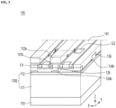
- FIG. 5 is a three-dimensional cross-sectional view of the power semiconductor device 105 according to the second embodiment.
- FIGS. 6A and 6B are cross-sectional views along lines A-A' and B-B', respectively, of the power semiconductor device 105 shown in FIG. 5 .
- the second embodiment is a planar MOSFET structure, and the technical features of first embodiment described above can be adopted. Accordingly, the description will focus on the features of second embodiment.
- the power semiconductor device 105 may include a drain electrode 160 (see FIG. 6A ), a substrate 110, and an epi layer 110E, the first wells 121 of second conductivity type, the first conductivity type source area 141, the source contact area 142 (see FIG. 6A ), and the second conductivity type contact area 123, a source electrode 140 (see FIG. 6A ), a second gate insulating layer 131b, a second gate 132b, and an interlayer insulating layer 150 (see FIG. 6A ).
- the epi layer 110E may include a first epi layer 111 of first conductivity type and a second epi layer 112 of first conductivity type.
- the second embodiment may include first wells 121 of second conductivity type, a third well 124b of second conductivity type, and an ion implantation connection region 126 of second conductivity type.
- the second gate insulating layer 131b may be formed through a thermal oxidation or deposition process on the first conductivity type source region 141, the first wells 121 of second conductivity type, and the second epitaxial layer 112 of first conductivity type.
- the second gate 132b may be formed on the second gate insulating layer 131b through a polysilicon deposition process.
- the second embodiment may include a third well 124b of second conductivity type disposed on the second epi layer 112 of first conductivity type on the lower side between spaced apart first wells 121 of second conductivity type. Additionally, the second embodiment may include an ion implantation connection region 126 of second conductivity type connecting the first wells 121 of second conductivity type to the third well 124b of second conductivity type.
- the third well 124b of second conductivity type may be disposed on the lower side between the spaced apart first wells 121 of second conductivity type.
- the horizontal width of the third well 124b of second conductivity type may be formed to be greater than or equal to the distance between the first wells 121 of second conductivity type, which is the width of the JFET.
- the third well 124b of second conductivity type is disposed below the region between the spaced apart first wells 121 of second conductivity type, and can be arranged continuous form along the second gate region.
- the third well 124b of second conductivity type may be arranged to extend horizontally in the first direction Y, which is the direction in which the second gate 132b extends.
- the ion implantation connection region 126 of second conductivity type is arranged to extend in the second direction (X) perpendicular to the first direction (Y), which is the extending direction of second gate (132b).
- the ion implantation connection region 126 of second conductivity type may be arranged to be spaced apart in the first direction (Y), may connect the third well 124b of second conductivity type arranged horizontally in the first direction (Y) and may be arranged to extend in a second direction (X) perpendicular to the first direction (Y).
- the third well 124b of second conductivity type is disposed below the area between the first wells 121 of second conductivity type, which are JFET regions, there is a technical effect of dispersing the electric field concentrated at the corner of first wells 121 of second conductivity type.
- the first wells 121 of second conductivity type to which the ground potential is applied is connected to the third well 124b of the second conductivity type by the ion implantation connection region 126 of second conductivity type by being connected to the third well 124b, a ground potential can also be applied to the third well 124b of second conductivity type.
- Ron On-resistance
- FIGS. 7A and 7B are cross-sectional views of the power semiconductor device 106 according to the third embodiment, respectively.
- the third embodiment may adopt the technical features of first or second embodiment described above, and the description will focus on the features of the third embodiment below.
- the third embodiment may include a first ion implantation connection region 126a of second conductivity type and a second ion implantation connection region 126b of second conductivity type.
- the ion implantation connection region 126 of second conductivity type has a structure that continually connects the third well 124b of second conductivity type of the adjacent cell in a stripe structure (see FIG. 5 ).
- the first ion implantation connection region 126a of second conductivity type or the second ion implantation connection region 126b of second conductivity type intersects on a cell basis to form a structure that connects the third well 124b of second conductivity type.
- FIGS. 7A and 7B may be cross-sectional views of first cell region and the second cell region of the power semiconductor device 106 according to the third embodiment.
- the first ion implantation connection region 126a of second conductivity type is disposed on one side, for example, on the left side, of second gate 132b.
- the first ion implantation connection region 126a of second conductivity type may connect the third well 124b of second conductivity type to the first wells 121 of second conductivity type.
- first ion implantation connection region 126a of second conductivity type may be disposed on the lower side between the second gates 132b of first cell region and the second gates 132b of the third cell region adjacent to the second gate 132b of first cell region in the positive (+) direction.
- the first ion implantation connection region 126a of second conductivity type may connect the third well 124b of second conductivity type disposed below the second gate 132b of first cell region to the third well 124b of second conductivity type disposed below the second gate 132b in the third cell region adjacent to the first cell region in the positive direction of the X-axis.
- first ion implantation connection region 126a of second conductivity type may connect the third well 124b of second conductivity type of first cell region and the third well of second conductivity type 124b of the third cell region to the first wells 121 of second conductivity type on the upper side.
- the second ion implantation connection region 126b of second conductivity type is disposed on the other side, for example, on the right side, of second gate 132b. So, the third well 124b of second conductive type may be connected to the upper first wells 121 of second conductive type.
- the second ion implantation connection region 126b of second conductivity type may be disposed on the lower side between the second gates 132b of second cell region and the second gate 132b of the fourth cell region in the negative (-) direction of second cell region.
- the second ion implantation connection region 126b of second conductivity type may connect the third well 124b of second conductivity type below the second gate 132b of second cell region to the third well 124b of second conductivity type disposed below the second gate 132b in the fourth cell region adjacent to the second cell region in the negative (-) direction of the X-axis.
- the second ion implantation connection region 126b of second conductivity type may connect the third well 124b of second conductivity type in the second cell region and the third well 124b of second conductivity type in the fourth cell region to the first wells 121 of second conductivity type on the upper side.
- the third well 124b of second conductivity type is disposed below the area between the first wells 121 of second conductivity type, which are JFET regions, so that there is a technical effect of dispersing the electric field concentrated at the corner of first wells 121 of second conductivity type.
- the first wells 121 of second conductivity type to which the ground potential is applied is connected to the third well 124b of the second conductivity type by the ion implantation connection region 126 of second conductivity type, a ground potential can also be applied to the third well 124b of second conductivity type.
- Ron On-resistance
- the first ion implantation connection region 126a of second conductivity type or the second ion implantation connection region 126b of second conductivity type can be disposed below only on one side or part of the other side of second gate 132b of each cell, so there is a complex technical effect that can improve current flow.
Landscapes
- Engineering & Computer Science (AREA)
- Power Engineering (AREA)
- Electrodes Of Semiconductors (AREA)
- Semiconductor Integrated Circuits (AREA)
Abstract
A power semiconductor device may include a substrate, a first epitaxial layer of first conductivity type disposed on the substrate, a second epi layer of first conductivity type disposed on the first epi layer of first conductivity type, first wells of second conductivity type spaced apart disposed on the second epi layer of first conductivity type, a third well of second conductivity type disposed in the second epi layer of first conductivity type below the spaced apart first wells of second conductivity type and an ion implantation connection region of second conductivity type configured to connect the first wells of second conductivity type to the third well of second conductivity type.
Description
- The embodiment relates to a power semiconductor device, a power semiconductor module, a power converter, and a method of manufacturing the same.
- Power semiconductors are one of the key elements that determine the efficiency, speed, durability, and reliability of power electronic systems.
- With the recent development of the power electronics industry, the previously used silicon (Si) power semiconductors have reached their physical limits. And to replace silicon power semiconductor, research is being actively conducted on WBG (wide bandgap) power semiconductors such as silicon carbide (SiC) and gallium nitride (GaN).
- WBG power semiconductor devices have a band gap energy that is approximately three times that of Si power semiconductor devices. Due to this, WBG power semiconductor device has the characteristics of low intrinsic carrier concentration, high breakdown electric field (about 4 to 20 times), high thermal conductivity (about 3 to 13 times), and large electron saturation rate (about 2 to 2.5 times).
- These characteristics enable operation in high temperature and high voltage environments and have high switching speed and low switching loss. Among these, gallium nitride (GaN) power semiconductor devices can be used in low-voltage systems, and silicon carbide (SiC) power semiconductor devices can be suitable for high-voltage systems.
- SiC MOSFET power semiconductors of the prior art are generally denoted as VDMOSFET with a vertical diffused structure, and may also be simply denoted as double-diffused structure DMOSFET. Additionally, SiC MOSFET can be classified into Planar MOSFET and Trench MOSFET depending on the direction of the channel.
- Among these, Trench MOSFET is a structure in which a channel is formed on the sidewall of the trench. For this, a gate insulating film is formed on the sidewall of the trench and a gate electrode is formed in the trench.
- Since SiC MOSFET have high ON-resistance (Ron) due to low channel mobility and large channel resistance, trench MOSFET were proposed to reduce this. Trench MOSFET has the advantage of increasing channel density by forming channels on the sidewalls of the trench.
- However, the trench MOSFET has a larger electric field in the trench gate oxide, which has a shorter drift distance than the P-base (P-well). In particular, since the electric field is concentrated at the trench edge of the trench, there is a problem that gate oxide breakdown occurs quickly and the breakdown voltage (BV) decreases.
- For example, in the case of SiC Trench MOSFET, the breakdown field strength is 10 times that of silicon (Si), so SiC semiconductor devices are used with a voltage close to 10 times that of Si devices. For this reason, an
electric field 10 times stronger than that of the silicon device is applied to the gate insulating film formed in the trench, causing a problem in which the gate insulating film is easily destroyed at the corners of the trench. - In internal technology, research was conducted to place a bottom P-well under the trench to prevent electric field concentration at the trench corner of the SiC Trench MOSFET.
- However, although the bottom P-well to prevent electric field concentration at the corner of the trench contributes to preventing breakdown voltage drop, there is a technical contradiction in that the On-resistance (Ron) increases due to the bottom P-well.
- One of the technical objects of the embodiment is to solve the technical contradiction of preventing breakdown voltage drop and increasing on-resistance (Ron) due to preventing electric field concentration at the corner of the trench. For example, the embodiment is intended to prevent the On-resistance from increasing while preventing electric field concentration in the bottom P-well at the corner of the trench.
- At least one of these objects is solved by the features of the independent claim(s).
- The technical problems of the embodiments are not limited to those described in this item and include those that can be understood through the description of the invention.
- A power semiconductor device according to an embodiment includes a substrate, a first epitaxial ("epi") layer of a first conductivity type disposed on the substrate, a second epi layer of the first conductivity type disposed on the first epi layer of first conductivity type, first wells of the second conductivity type spaced apart from each other and disposed on or in the second epi layer of the first conductivity type, a third well of the second conductivity type disposed in the second epi layer of the first conductivity type and below the spaced apart first wells of the second conductivity type and an ion implantation connection region of the second conductivity type configured to connect the first wells of the second conductivity type to the third well of the second conductivity type.
- A power semiconductor device according to an embodiment includes a
substrate 110, afirst epi layer 111 of a first conductivity type disposed on thesubstrate 110, and asecond epi layer 112 of the first conductivity type disposed on thefirst epi layer 111 of the first conductivity type, andfirst wells 121 of a second conductivity type spaced apart from each other and disposed on or in thesecond epi layer 112 of the first conductivity type. The power semiconductor device may further include a source region of thefirst conductivity type 141 disposed on at least one of thefirst wells 121 of the second conductivity type. The power semiconductor device may further include a secondgate insulating layer 131b disposed on at least one of the source region of thefirst conductivity type 141, and said at least one of thefirst wells 121 of the second conductivity type and thesecond epi layer 112 of the first conductivity type, and asecond gate 132b disposed on the secondgate insulating layer 131b. The power semiconductor device may include athird well 124b of the second conductivity type disposed in or on thesecond epi layer 112 of the first conductivity type below the spaced apartfirst wells 121 of the second conductivity type (and/or on a lower side between the spaced apartfirst wells 121 of the second conductivity type). The power semiconductor device may include a ionimplantation connection region 126 of the second conductivity type connecting thefirst wells 121 of the second conductivity type and thethird well 124b of the second conductivity type. - When a ground potential is applied to the
first wells 121 of the second conductivity type, a ground potential may also be applied to thethird well 124b of the second conductivity type is formed by the ionimplantation connection region 126 of the second conductivity type. - A horizontal width of the
third well 124b of the second conductivity type may be greater than or equal to a distance between thefirst wells 121 of the second conductivity type. - The
third well 124b of the second conductivity type may be disposed below a region between the spaced apartfirst wells 121 of the second conductivity type. The second gate may be disposed in a continuous form along a region of second gate. Thethird well 124b of the second conductivity type may be arranged in a continuous form along the second gate. - The
third well 124b of the second conductivity type may be arranged to extend (e.g. horizontally) in a first direction (Y), which is the direction in which thesecond gate 132b extends. - The ion
implantation connection region 126 of the second conductivity type may be arranged to extend in a second direction (X) perpendicular to the first direction (Y). - The ion
implantation connection region 126 of the second conductivity type may be arranged to extend in the second direction (X) perpendicular to the first direction (Y) while connecting thethird well 124b of the second conductivity type disposed horizontally in the first direction (Y) while being spaced apart in the first direction (Y). - The ion
implantation connection region 126 of the second conductivity type may include a first ionimplantation connection region 126a of the second conductivity type connecting thethird well 124b of the second conductivity type disposed below thesecond gate 132b of a first cell region to thethird well 124b of the second conductivity type disposed below thesecond gate 132b of a third cell region adjacent in the positive direction of said first cell region. A cell region may denote a region which includes a gate, a source region and a drain region. The third cell region may be disposed adjacent at a left side of the first cell region. In addition, a second cell region may be disposed adjacent at a right side of the first cell region. In addition, a fourth cell region may be disposed adjacent at a right side of the second cell region. - The third well of the second conductivity type may include a third-first well of the second conductivity type disposed below the second gate of a first cell region, and a third-second well of the second conductivity type disposed below the second gate of a third cell region adjacent to a positive X-axis direction of the first cell region. The ion implantation connection region of the second conductivity type may include a first ion implantation connection region of the second conductivity type connecting the third-first well of second conductivity type to the third-second well of the second conductivity type. When a ground potential is applied to the first wells of the second conductivity type, a ground potential may also be applied to the third well of the second conductivity type by the ion implantation connection region of the second conductivity type. A horizontal width of the third-first well of the second conductivity type may be greater than or equal to a distance between the first wells of the second conductivity type.
- The first ion
implantation connection region 126a of the second conductivity type may connect thethird well 124b of the second conductivity type of the first cell region and thethird well 124b of the second conductivity type of the third cell region to thefirst wells 121 of the second conductivity type on the upper side. - The ion
implantation connection region 126 of the second conductivity type may include a second ionimplantation connection region 126b of the second conductivity type connecting thethird well 124b of the second conductivity type disposed below thesecond gate 132b of the second cell region to thethird well 124b of the second conductivity type disposed below thesecond gate 132b of the fourth cell region adjacent in the negative (-) direction of the X-axis of second cell region. - The second ion
implantation connection region 126b of the second conductivity type may connect thethird well 124b of the second conductivity type of second cell region andthird well 124b of the second conductivity type well of the fourth cell region to thefirst wells 121 of the second conductivity type on the upper side. - According to an embodiment, a power converter may include any of the above described power semiconductor devices.
- According to the power semiconductor device, the power converter including the same, and the manufacturing method of the power semiconductor device according to the embodiment, there is a technical effect that it can solve the problem of increasing on-resistance (Ron) while preventing electric field concentration at the trench corner or the problem that adversely affect the electrical characteristics of the power semiconductor device.
- For example, according to an embodiment, since the
second well 124 of second conductivity type is disposed on the bottom side of the trench, and is disposed in a continuous form along the trench area, there is a technical effect of dispersing the electric field concentrated at the corner of the trench, preventing the breakdown voltage drop of the gate insulating layer, and improving the reliability of the gate insulating layer. - Additionally, according to the embodiment, the ion
implantation connection region 126 of second conductivity type may connect thesecond well 124 of second conductivity type and thefirst wells 121 of second conductivity type. Accordingly, thefirst wells 121 of second conductivity type to which the ground potential is applied is connected to thesecond well 124 of second conductivity type by the ionimplantation connection region 126 of second conductivity type, allowing thesecond well 124 of second conductivity type to also be at ground potential. - In addition, according to the embodiment, since the
second well 124 of second conductivity type does not directly contact the bottom of the gate trench, there is an advantage in terms of thickness and characteristics that there is a reduced risk of forming an unexpectedly grown oxide layer during the thermal oxidation process for forming the gate insulating layer. - In addition, according to the embodiment, by applying a ground potential to the second conductivity type second
well 124 that prevents electric field concentration at the trench corners, it is possible to prevent the formation of depletion regions in the second conductivity type secondwell 124, thereby preventing an increase in On-resistance (Ron). - Also, according to the second embodiment, the
first wells 121 of second conductivity type to which the ground potential is applied is connected to thethird well 124b of second conductivity type by the ionimplantation connection region 126 of second conductivity type. Accordingly, the ground potential may also be applied to thethird well 124b of second conductivity type. Therefore, there is a complex technical effect of preventing an increase in on-resistance (Ron) by applying the ground potential to thethird well 124b of second conductivity type, which prevents electric field concentration. - Also, according to the third embodiment, the first ion
implantation connection region 126a of second conductivity type or the second ionimplantation connection region 126b of second conductivity type can be disposed only on one side or the other side below thesecond gate 132b of each cell, there is a complex technical effect that can improve current flow. - The technical effects of the embodiments are not limited to those described in this item and include those that can be understood through the description of the invention.
-
-
FIG. 1 is an exemplary configuration diagram of apower converter 1000 according to an embodiment. -
FIG. 2 is a cross-sectional view of apower semiconductor device 100 according to an embodiment. -
FIG. 3 is a three-dimensional cross-sectional view of thepower semiconductor device 101 according to the first embodiment. -
FIGS. 4A and4B are cross-sectional views taken along lines A-A' and B-B', respectively, of thepower semiconductor device 101 shown inFIG. 3 . -
FIG. 5 is a three-dimensional cross-sectional view of thepower semiconductor device 105 according to the second embodiment. -
FIGS. 6A and6B are cross-sectional views along lines A-A' and B-B', respectively, of thepower semiconductor device 105 shown inFIG. 5 . -
FIGS. 7A and7B are cross-sectional views of thepower semiconductor device 106 according to the third embodiment, respectively. - Hereinafter, embodiments are described in detail with reference to the drawings.
- The suffixes "module" and "unit" for the elements used in the following description are simply given in consideration of ease of writing this specification, and do not themselves give a particularly important meaning or role. Accordingly, the "module" and "unit" can be used interchangeably.
- Terms including ordinal numbers, such as first and second, can be used to describe various elements, but the elements are not limited by the terms. These terms are only used for the purpose of distinguishing one element from another.
- Singular expressions include plural expressions unless the context clearly dictates otherwise.
- In this application, terms such as "comprise", "have" or "include" are intended to designate that there is a feature, number, step, operation, component, part, or combination thereof described in the specification, and it is not precluded from being excluded one or other features, numbers, steps, operations, components, parts, or combinations thereof, or any combination thereof.
-
FIG. 1 is a circuit diagram of apower converter 1000 according to an embodiment. - The
power converter 1000 according to the embodiment can receive DC power from a battery or fuel cell, convert it into AC power, and supply AC power to a predetermined load. For example, thepower converter 1000 according to the embodiment can include an inverter, which receive DC power from a battery, convert DC power into 3-phase AC power, and supply 3-phase AC power to a motor M. And motor M can provide power to electric vehicles or fuel cell vehicles. - The
power converter 1000 according to the embodiment can include thepower semiconductor device 100. Thepower semiconductor device 100 can be a Metal Oxide Semiconductor Field Effect Transistor (MOSFET), but is not limited thereto, and can include an Insulated Gate Bipolar Transistor (IGBT). - For example, the
power converter 1000 can include a plurality ofpower semiconductor devices power semiconductor devices - In the embodiment, DC power can be converted into AC power through on-off control of the plurality of
power semiconductor devices 100a to 100f. For example, in thepower converter 1000 according to the embodiment, the firstpower semiconductor device 100a can be turned on and the secondpower semiconductor device 100b can be turned off in a first time period of one cycle to supply positive polarity power to the motor M. In addition, in the second time period of one cycle, the firstpower semiconductor device 100a can be turned off and the secondpower semiconductor device 100b can be turned on to supply negative polarity power to the motor M. - In the embodiment, a group of power semiconductor devices disposed in series in a high voltage line and a low voltage line of an input side can be referred to as an arm. For example, the first
power semiconductor device 100a and the secondpower semiconductor device 100b can constitute a first arm, and the thirdpower semiconductor device 100c and the fourthpower semiconductor device 100d can constitute a second arm. And the fifthpower semiconductor device 100e and the sixthpower semiconductor device 100f can constitute a third arm. - In the arm, an upper side power semiconductor device and a bottom side power semiconductor device can be controlled not to turn on at the same time. For example, in the first arm, the first
power semiconductor device 100a and the secondpower semiconductor device 100b do not simultaneously turn on, but can turn on and off alternately. - Each of the
power semiconductor devices 100a to 100f can receive high power in an off state. For example, when the secondpower semiconductor device 100b is turned off while the firstpower semiconductor device 100a is turned on, the input voltage can be applied to the secondpower semiconductor device 100b as it is. The voltage input to the secondpower semiconductor device 100b can be a relatively high voltage, and a withstand voltage of eachpower semiconductor device 100a to 100f can be designed to have a high level to withstand such a high voltage. - Each of the
power semiconductor devices 100a to 100f can conduct a high current in a turn on state. The motor M can be driven with a relatively high current, and this high current can be supplied to the motor M through a power semiconductor device that is turned on. - A high voltage applied to each of the
power semiconductor devices 100a to 100f can cause a high switching loss. A high current conducting thepower semiconductor devices 100a to 100f can cause a high conduction loss. In order to dissipate heat generated by such switching loss or conduction loss, thepower semiconductor devices 100a to 100f can be packaged as a power semiconductor module including a heat dissipation means. - The
power semiconductor device 100 of the embodiment can be a silicon carbide (SiC) power semiconductor device, can operate in a high-temperature, high-voltage environment, and can have a high switching speed and low switching loss. - Meanwhile, the
power converter 1000 according to the embodiment can include a plurality of power semiconductor modules. - For example, the plurality of
power semiconductor devices 100a to 100f shown inFIG. 1 can be packaged into one power semiconductor module, or the power semiconductor devices constituting each arm can be packaged into one power semiconductor module. - For example, the first
power semiconductor device 100a, the secondpower semiconductor device 100b, the thirdpower semiconductor device 100c, the fourthpower semiconductor device 100d, and the fifthpower semiconductor device 100e and the sixthpower semiconductor device 100f shown inFIG. 1 can be packaged into one power semiconductor module. - In addition, there can be additional power semiconductor devices disposed in parallel with each of the
power semiconductor devices 100a to 100f to increase a current capacity. In this case, the number of power semiconductor devices included in the power semiconductor module can be greater than six. - The
power converter 1000 according to the embodiment can include a diode-type power semiconductor device in addition to the transistor-typepower semiconductor devices 100a to 100f. For example, a first diode (not shown) can be disposed in parallel with the firstpower semiconductor device 100a, and a second diode (not shown) can be disposed in parallel with the secondpower semiconductor device 100b. Also, these diodes can be packaged together in one power semiconductor module. In addition, the diode can be disposed in the form of an internal diode in each power semiconductor device. - Next, the power semiconductor devices constituting each arm can be packaged into one power semiconductor module.
- For example, the first
power semiconductor device 100a and the secondpower semiconductor device 100b constituting the first arm can be packaged as a first power semiconductor module. The thirdpower semiconductor device 100c and the fourthpower semiconductor device 100d constituting the second arm can be packaged into a second power semiconductor module. And the fifthpower semiconductor device 100e and the sixthpower semiconductor device 100f constituting the third arm can be packaged into a third power semiconductor module. - In addition, there can be additional power semiconductor devices arranged in parallel with each
power semiconductor device 100a to 100f to increase a current capacity. In this case, the number of power semiconductor devices included in each power semiconductor module can be more than two. Also, each arm can include a diode-type power semiconductor device (not shown) in addition to the transistor-typepower semiconductor devices 100a to 100f, and these diodes can also be packaged together in one power semiconductor module. In addition, the diode can be disposed in a form of an internal diode in each power semiconductor device. - Next,
FIG. 2 is a cross-sectional view of one of thepower semiconductor devices 100 according to an embodiment. - The
power semiconductor device 100 according to the embodiment may include asource electrode 140, agate electrode 130 arranged to be spaced apart from each other on the upper side of a predeterminedsemiconductor epitaxial layer 110E, and adrain electrode 160 disposed below thesemiconductor epitaxial layer 110E. - In the form of a MOSFET, the
source electrode 140 or thegate electrode 130 may include an Al-based metal and may include a Ni layer, a Ti layer, a Ni/Ti layer, or a TiN/Ti silicide layer. - The
drain electrode 160 may include a Ni-based metal and may include a Ti layer, a Ni layer, or an Ag layer. For example, thedrain electrode 160 may include Ti/Ag, Ti/Ni/Ag, NiV/Ag, or V(vanadium)/Ni/Ag, etc., but is not limited thereto. - One of the technical objects of the embodiment is to solve the technical contradiction of preventing breakdown voltage drop and increasing on-resistance (Ron) due to preventing electric field concentration at the corner of the trench.
- Hereinafter, technical features of a power semiconductor device according to an embodiment for solving the above technical problems will be described.
-
FIG. 3 is a three-dimensional cross-sectional view of thepower semiconductor device 101 according to the first embodiment. -
FIGS. 4A and4B are cross-sectional views along lines A-A' and B-B', respectively, of thepower semiconductor device 101 shown inFIG. 3 . Hereinafter, `first embodiment' may be abbreviated and described as 'embodiment'. - Referring to
FIGS. 3 ,4A , and4B , thepower semiconductor device 101 according to the first embodiment may include a drain electrode 160 (seeFIG. 4A ), asubstrate 110, anepi layer 110E,first wells 121 of second conductivity type, a first conductivitytype source area 141, a source contact area 142 (seeFIG. 4A ), a second conductivity type contact area 123 (seeFIG. 4B ), a source electrode 140 (seeFIG. 4A ), agate insulating layer 131, atrench gate 132, and an interlayer insulating layer 150 (seeFIG. 4A ). - The
epi layer 110E may include afirst epi layer 111 of first conductivity type and asecond epi layer 112 of first conductivity type. - Additionally, the embodiment may include
first wells 121 of second conductivity type, asecond well 124 of second conductivity type, and an ionimplantation connection region 126 of second conductivity type. - The first conductivity type may be N-type, and the second conductivity type may be P-type, but are not limited thereto. For example, the N-type dopant may be implanted with N or P, but is not limited thereto. Additionally, the P-type dopant may be implanted with Al or Boron, but is not limited thereto.
- Specifically, referring to
FIGS. 4A and4B , thepower semiconductor device 101 according to the embodiment may include asubstrate 110 and afirst epi layer 111 of first conductivity type disposed on thesubstrate 110 and asecond epi layer 112 of first conductivity type disposed on thefirst epi layer 111 of first conductivity type. - The
substrate 110, thefirst epitaxial layer 111 of first conductivity type, and thesecond epitaxial layer 112 of first conductivity type may include silicon carbide (SiC) and may be doped into N-type, but are not limited thereto. For example, thesubstrate 110 and the first and second epi layers 111 and 112 of first conductivity type may include a 4H-SiC material, but are not limited thereto. For example, thesubstrate 110 and the first and second epi layers 111 and 112 of first conductivity type may include 3C-SiC or 6H-SiC. - The
first epi layer 111 of first conductivity type may include a first conductivity type buffer layer (not shown) and a first conductivity type drift layer (not shown). Thefirst epi layer 111 of first conductivity type is doped at a lower concentration than thesubstrate 110, thereby preventing a breakdown voltage (VB) drop. - In addition, the
second epitaxial layer 112 of first conductivity type is doped at a higher concentration than thefirst epitaxial layer 111 of first conductivity type, allowing the second epitaxial layer (112) of first conductivity type to function as a current spreading layer (CSL) and thereby reducing the on-resistance. - The
first wells 121 of second conductivity type may be formed by ion implantation of second conductivity type dopant into thesecond epi layer 112 of first conductivity type or by growing the second conductivity type epi layer. Thefirst wells 121 of second conductivity type may be referred to as a second conductivity type base layer, but is not limited thereto. - Referring to
FIG. 4B , the first conductivitytype source area 141 and the second conductivitytype contact area 123 may be formed by ion implantation into thefirst wells 121 of second conductivity type. - The doping concentration of first conductivity
type source area 141 and the second conductivitytype contact area 123 may be higher than that offirst wells 121 of second conductivity type. The second conductivetype contact area 123 may be partially formed as shown inFIG. 3 . The second conductivitytype contact area 123 may function to maintain the zero potential offirst wells 121 of second conductivity type. - Next, the
gate insulating layer 131 can be formed by thermal oxidation or deposition process on a bottom and sidewall of the trench area where the first conductivitytype source area 141, thefirst wells 121 of second conductivity type and thesecond epi layer 112 of first conductivity type has been removed. - Next, a
trench gate 132 may be formed on the trench above thegate insulating layer 131 through a process involving polysilicon deposition and etch-back. - Next, a
source contact area 142 may be formed on first conductivetype source area 141 and/or the second conductivetype contact area 123. For example, thesource contact area 142 may be formed using Ti or Ni, but is not limited thereto. - Next, the
interlayer insulating layer 150 may be formed on thetrench gate 132 through a deposition process such as an oxide film. - Next, a
source electrode 140, a gate electrode (not shown), and adrain electrode 160 may be formed. - For example, the
source electrode 140 or thegate electrode 130 may include an Al-based metal and may include a Ni layer, a Ti layer, a Ni/Ti layer, or a TiN/Ti silicide layer. Additionally, thedrain electrode 160 may include a Ni-based metal and may include a Ti layer, a Ni layer, and an Ag layer. For example, thedrain electrode 160 may include Ti/Ag, Ti/Ni/Ag, or NiV/Ag, V(vanadium)/Ni/Ag, etc., but is not limited thereto. - Next, referring to
FIG. 4B , the embodiment may include asecond well 124 of second conductivity type disposed on thesecond epi layer 112 of first conductivity type and spaced apart from thegate insulating layer 131 and thefirst wells 121 of second conductivity type. Also, the embodiment may include an ionimplantation connection region 126 of second conductivity type connecting thefirst wells 121 of second conductivity type and the second well 124 of second conductivity type. - The second well 124 of second conductivity type is disposed below the trench.
- The ion
implantation connection region 126 of second conductivity type may be doped at a concentration lower than that of second well 124 of second conductivity type, but is not limited thereto. - Referring to
FIG. 3 , the second well 124 of second conductivity type is disposed below the trench and may be disposed in a continuous form along the trench area. - The second well 124 of second conductivity type can be formed by high-energy ion implantation or by using a re-growth process. For example, after growing the
second epi layer 112 of first conductivity type on thefirst epi layer 111 of first conductivity type, the second well 124 of second conductivity type may be formed through high-energy ion implantation. Alternatively, after forming thefirst epi layer 111 of first conductivity type, the second well 124 of second conductivity type may be formed by ion implantation, and then thesecond epi layer 112 of first conductivity type may be formed. - The second well 124 of second conductivity type may be arranged to extend horizontally in the first direction Y, which is which is the extension direction of the
trench gate 132. - On the other hand, the ion
implantation connection region 126 of second conductivity type may be arranged to extend in the second direction X perpendicular to the first direction Y, which is the extension direction of thetrench gate 132. - The ion
implantation connection region 126 of second conductivity type can be arranged to extend vertically in the second direction X while connecting the horizontally arranged the second well 124 of second conductivity type in the first direction Y, which is offset in the first direction Y. - The top of second conductivity type ion
implantation connection region 126 may be disposed higher than the bottom of thegate insulating layer 131, and the bottom of second conductivity type ionimplantation connection region 126 may be disposed lower than the bottom of thegate insulation layer 131. - According to the power semiconductor device, the power converter including the same, and the manufacturing method of the power semiconductor device according to the embodiment, there are technical effects that can be solve the problem of increasing on-resistance (Ron) while preventing electric field concentration at the corner of the trench or affecting negative impact to characteristics of the power semiconductor device.
- For example, according to an embodiment, the second well 124 of second conductivity type is disposed on the bottom side of the trench, and is disposed in a continuous form along the trench area, there is a technical effect of dispersing the electric field concentrated at the corner of the trench, preventing the breakdown voltage drop of the gate insulating layer, and improving the reliability of the gate insulating layer.
- Additionally, according to the embodiment, the ion
implantation connection region 126 of second conductivity type may connect the second well 124 of second conductivity type and thefirst wells 121 of second conductivity type. Accordingly, thefirst wells 121 of second conductivity type to which the ground potential is applied is connected to the second well 124 of second conductivity type by the ionimplantation connection region 126 of second conductivity type, allowing the second well 124 of second conductivity type to also be at ground potential. - In addition, according to the embodiment, since the second well 124 of second conductivity type does not directly contact the bottom of the gate trench, there is an advantage in terms of thickness and characteristics that there is a reduced risk of forming an unexpectedly grown oxide layer during the thermal oxidation process for forming the gate insulating layer.
- Meanwhile, in internal technology, research was conducted to place a bottom P-well under the trench to prevent electric field concentration at the corner of the trench.
- First, using the first internal technology, a 'floating bottom P-well' was formed in a floating state spaced apart from the trench gate and gate insulating layer.
- This 'floating bottom P-well' has the effect of preventing a breakdown voltage drop by relieving the electric field concentration at the corner of the trench, but a problem was studied in which charging and discharging continuously occur repeatedly inside the floating bottom P-well, thereby affecting the potential around the floating bottom P-well.
- In other words, the problem of adversely affecting the electrical characteristics of power semiconductor devices was studied by generating an unknown internal potential in the floating bottom P-well in addition to the applied external potential.
- Additionally, the floating bottom P-well interferes with current flow in the on state, causing an increase in ON-resistance (Ron/RDS), which is the resistance between drain and source.
- Next, using the second internal technology, a 'contacted bottom P-well' was formed on the bottom side of the trench to contact the trench gate insulating layer.
- However, when a 'contacted bottom P-well' is formed at the bottom of the trench to be in contact with the trench gate insulating layer, there is an effect of alleviating electric field concentration at the trench corner, but the problem of deterioration of forward current characteristics due to an increase in the width of the depletion layer in the 'contacted bottom P-well' in contact with the gate insulating layer according to the drain voltage was studied.
- Additionally, when the 'contacted bottom P-well' is formed close to the P-base (P-well) to be in contact with the trench gate insulating layer, the problem of increasing ON-resistance (Ron) due to JFET resistance occurring between the P-base (P-well) and the bottom P-well in contact was studied.
- On the other hand, referring to
FIGS. 3 and4B , in the embodiment, the ionimplantation connection region 126 of second conductivity type may connect the second well 124 of second conductivity type and thefirst wells 121 of second conductivity type. Accordingly, thefirst wells 121 of second conductivity type to which the ground potential is applied is connected to the second well 124 of second conductivity type by the ionimplantation connection region 126 of second conductivity type, allowing the second well 124 of second conductivity type to also be at ground potential. - Therefore, according to the embodiment, by applying a ground potential to the second well 124 of second conductivity type that prevents electric field concentration at the trench corners, it is possible to prevent the formation of depletion regions in the second conductivity type second well 124, thereby preventing an increase in On-resistance (Ron).
- Next,
FIG. 5 is a three-dimensional cross-sectional view of thepower semiconductor device 105 according to the second embodiment. -
FIGS. 6A and6B are cross-sectional views along lines A-A' and B-B', respectively, of thepower semiconductor device 105 shown inFIG. 5 . - The second embodiment is a planar MOSFET structure, and the technical features of first embodiment described above can be adopted. Accordingly, the description will focus on the features of second embodiment.
- Referring to
FIGS. 5 ,6A , and6B , thepower semiconductor device 105 according to the second embodiment may include a drain electrode 160 (seeFIG. 6A ), asubstrate 110, and anepi layer 110E, thefirst wells 121 of second conductivity type, the first conductivitytype source area 141, the source contact area 142 (seeFIG. 6A ), and the second conductivitytype contact area 123, a source electrode 140 (seeFIG. 6A ), a secondgate insulating layer 131b, asecond gate 132b, and an interlayer insulating layer 150 (seeFIG. 6A ). - The
epi layer 110E may include afirst epi layer 111 of first conductivity type and asecond epi layer 112 of first conductivity type. - Additionally, the second embodiment may include
first wells 121 of second conductivity type, athird well 124b of second conductivity type, and an ionimplantation connection region 126 of second conductivity type. - In the second embodiment, the second
gate insulating layer 131b may be formed through a thermal oxidation or deposition process on the first conductivitytype source region 141, thefirst wells 121 of second conductivity type, and thesecond epitaxial layer 112 of first conductivity type. - Additionally, the
second gate 132b may be formed on the secondgate insulating layer 131b through a polysilicon deposition process. - Next, referring to
FIGS. 5 and6B , the second embodiment may include athird well 124b of second conductivity type disposed on thesecond epi layer 112 of first conductivity type on the lower side between spaced apartfirst wells 121 of second conductivity type. Additionally, the second embodiment may include an ionimplantation connection region 126 of second conductivity type connecting thefirst wells 121 of second conductivity type to thethird well 124b of second conductivity type. - The
third well 124b of second conductivity type may be disposed on the lower side between the spaced apartfirst wells 121 of second conductivity type. - The horizontal width of the
third well 124b of second conductivity type may be formed to be greater than or equal to the distance between thefirst wells 121 of second conductivity type, which is the width of the JFET. - Referring to
FIG. 5 , thethird well 124b of second conductivity type is disposed below the region between the spaced apartfirst wells 121 of second conductivity type, and can be arranged continuous form along the second gate region. - The
third well 124b of second conductivity type may be arranged to extend horizontally in the first direction Y, which is the direction in which thesecond gate 132b extends. - On the other hand, the ion
implantation connection region 126 of second conductivity type is arranged to extend in the second direction (X) perpendicular to the first direction (Y), which is the extending direction of second gate (132b). - The ion
implantation connection region 126 of second conductivity type may be arranged to be spaced apart in the first direction (Y), may connect thethird well 124b of second conductivity type arranged horizontally in the first direction (Y) and may be arranged to extend in a second direction (X) perpendicular to the first direction (Y). - According to the second embodiment, since the
third well 124b of second conductivity type is disposed below the area between thefirst wells 121 of second conductivity type, which are JFET regions, there is a technical effect of dispersing the electric field concentrated at the corner offirst wells 121 of second conductivity type. - In addition, according to the second embodiment, the
first wells 121 of second conductivity type to which the ground potential is applied is connected to thethird well 124b of the second conductivity type by the ionimplantation connection region 126 of second conductivity type by being connected to thethird well 124b, a ground potential can also be applied to thethird well 124b of second conductivity type. - Accordingly, there is a complex technical effect of preventing an increase in On-resistance (Ron) by applying the ground potential to the
third well 124b of second conductivity type, which prevents electric field concentration. - Next,
FIGS. 7A and7B are cross-sectional views of thepower semiconductor device 106 according to the third embodiment, respectively. - The third embodiment may adopt the technical features of first or second embodiment described above, and the description will focus on the features of the third embodiment below.
- Unlike the second embodiment, the third embodiment may include a first ion
implantation connection region 126a of second conductivity type and a second ionimplantation connection region 126b of second conductivity type. - For example, in the second embodiment, the ion
implantation connection region 126 of second conductivity type has a structure that continually connects thethird well 124b of second conductivity type of the adjacent cell in a stripe structure (seeFIG. 5 ). - On the other hand, in the third embodiment, the first ion
implantation connection region 126a of second conductivity type or the second ionimplantation connection region 126b of second conductivity type intersects on a cell basis to form a structure that connects thethird well 124b of second conductivity type. - For example,
FIGS. 7A and7B may be cross-sectional views of first cell region and the second cell region of thepower semiconductor device 106 according to the third embodiment. - For example, referring to
FIG. 7A , in the first cell region, the first ionimplantation connection region 126a of second conductivity type is disposed on one side, for example, on the left side, ofsecond gate 132b. The first ionimplantation connection region 126a of second conductivity type may connect thethird well 124b of second conductivity type to thefirst wells 121 of second conductivity type. - For example, the first ion
implantation connection region 126a of second conductivity type may be disposed on the lower side between thesecond gates 132b of first cell region and thesecond gates 132b of the third cell region adjacent to thesecond gate 132b of first cell region in the positive (+) direction. - At this time, the first ion
implantation connection region 126a of second conductivity type may connect thethird well 124b of second conductivity type disposed below thesecond gate 132b of first cell region to thethird well 124b of second conductivity type disposed below thesecond gate 132b in the third cell region adjacent to the first cell region in the positive direction of the X-axis. - In addition, the first ion
implantation connection region 126a of second conductivity type may connect thethird well 124b of second conductivity type of first cell region and the third well ofsecond conductivity type 124b of the third cell region to thefirst wells 121 of second conductivity type on the upper side. - Also, referring to
FIG. 7B , in the second cell region, the second ionimplantation connection region 126b of second conductivity type is disposed on the other side, for example, on the right side, ofsecond gate 132b. So, thethird well 124b of second conductive type may be connected to the upperfirst wells 121 of second conductive type. - For example, the second ion
implantation connection region 126b of second conductivity type may be disposed on the lower side between thesecond gates 132b of second cell region and thesecond gate 132b of the fourth cell region in the negative (-) direction of second cell region. - At this time, the second ion
implantation connection region 126b of second conductivity type may connect thethird well 124b of second conductivity type below thesecond gate 132b of second cell region to thethird well 124b of second conductivity type disposed below thesecond gate 132b in the fourth cell region adjacent to the second cell region in the negative (-) direction of the X-axis. - In addition, the second ion
implantation connection region 126b of second conductivity type may connect thethird well 124b of second conductivity type in the second cell region and thethird well 124b of second conductivity type in the fourth cell region to thefirst wells 121 of second conductivity type on the upper side. - According to the third embodiment, the
third well 124b of second conductivity type is disposed below the area between thefirst wells 121 of second conductivity type, which are JFET regions, so that there is a technical effect of dispersing the electric field concentrated at the corner offirst wells 121 of second conductivity type. - In addition, according to the third embodiment, the
first wells 121 of second conductivity type to which the ground potential is applied is connected to thethird well 124b of the second conductivity type by the ionimplantation connection region 126 of second conductivity type, a ground potential can also be applied to thethird well 124b of second conductivity type. - Accordingly, there is a complex technical effect of preventing an increase in On-resistance (Ron) by applying the ground potential to the
third well 124b of second conductivity type, which prevents electric field concentration. - Also, according to the third embodiment, the first ion
implantation connection region 126a of second conductivity type or the second ionimplantation connection region 126b of second conductivity type can be disposed below only on one side or part of the other side ofsecond gate 132b of each cell, so there is a complex technical effect that can improve current flow. - Although the present invention has been described above with reference to embodiments, those skilled in the art can modify the present invention in various ways without departing from the scope of the present invention as set forth in the claims below. It will be easy to understand that and can be changed.
Claims (15)
- A power semiconductor device comprising:a substrate (110);a first epi layer (111) of a first conductivity type disposed on the substrate (110);a second epi layer (112) of the first conductivity type disposed on the first epi layer (111) of the first conductivity type;first wells (121) of a second conductivity type spaced apart from each other and disposed in the second epi layer (112) of the first conductivity type;at least one third well (124b) of the second conductivity type disposed in the second epi layer (112) of the first conductivity type and below the spaced apart first wells (121) of the second conductivity type; andan ion implantation connection region (126) of the second conductivity type arranged to connect the first wells (121) of the second conductivity type to the third well (124b) of the second conductivity type.
- The power semiconductor device according to claim 1, wherein the ion implantation connection region of the second conductivity type is configured to, when a ground potential is applied to the first wells (121) of the second conductivity type, apply the ground potential to the third well (124b) of the second conductivity type.
- The power semiconductor device according to claim 1 or 2, wherein a horizontal width of the third well (124b) of the second conductivity type is greater than or equal to a distance between the first wells (121) of the second conductivity type.
- The power semiconductor device according to any one of the preceding claims, wherein the third well (124b) of the second conductivity type is disposed below a region formed between the spaced apart first wells (121) of the second conductivity type.
- The power semiconductor device according to any one of the preceding claims,
further comprising:a source region (141) of the first conductivity type disposed on one of the first wells (121) of the second conductivity type;a second gate insulating layer (131b) disposed on the source region (141) of the first conductivity type, said one of the first wells (121) of the second conductivity type, and the second epi layer (112) of the first conductivity type; anda second gate (132b) disposed on the second gate insulating layer (131b). - The power semiconductor device according to claim 5, wherein the third well (124b) of the second conductivity type is arranged in a continuous form along the second gate (132b).
- The power semiconductor device according to claim 5 or 6, wherein the second gate (132b) extends in a first direction (Y) and the third well (124b) of the second conductivity type is arranged to extend in the first direction (Y).
- The power semiconductor device according to claim 7, wherein the ion implantation connection region (126) of the second conductivity type is arranged to extend in a second direction (X) perpendicular to the first direction (Y).
- The power semiconductor device according to any one of the preceding claims,
further comprising:a second gate insulating layer (131b) disposed on the first wells (121) of the second conductivity type and the second epi layer (112) of the first conductivity type; anda second gate (132b) disposed on the second gate insulating layer. - The power semiconductor device according to claim 9, wherein the third well of the second conductivity type comprises a third-first well of the second conductivity type disposed below the second gate of a first cell region, and a third-second well of the second conductivity type disposed below the second gate of a second cell region, wherein the second cell region is adjacent to the first cell region in a positive X-axis direction.
- The power semiconductor device according to claim 10, wherein the ion implantation connection region of the second conductivity type comprises a first ion implantation connection region of the second conductivity type connecting the third-first well of the second conductivity type to the third-second well of the second conductivity type.
- The power semiconductor device according to claim 11, wherein when a ground potential is applied to the first wells of the second conductivity type, the ground potential is also applied to the third well of the second conductivity type by the ion implantation connection region of the second conductivity type.
- The power semiconductor device according to claim 11 or 12, wherein a horizontal width of the third-first well of the second conductivity type is greater than or equal to a distance between the first wells of the second conductivity type.
- The power semiconductor device according to claim 11, 12 or 13, wherein the third-first well of the second conductivity type is disposed below a region between the spaced apart first wells of the second conductivity type, and is disposed in a continuous form along the second gate of the first cell region.
- A power converter comprising the power semiconductor device of any one of claims 1 to 14.
Applications Claiming Priority (1)
| Application Number | Priority Date | Filing Date | Title |
|---|---|---|---|
| KR1020230183770A KR20250093007A (en) | 2023-12-15 | 2023-12-15 | Power semiconductor device and power conversion device including the same |
Publications (1)
| Publication Number | Publication Date |
|---|---|
| EP4572562A1 true EP4572562A1 (en) | 2025-06-18 |
Family
ID=93923946
Family Applications (1)
| Application Number | Title | Priority Date | Filing Date |
|---|---|---|---|
| EP24219704.4A Pending EP4572562A1 (en) | 2023-12-15 | 2024-12-13 | Power semiconductor device and power converter including the same |
Country Status (6)
| Country | Link |
|---|---|
| US (1) | US20250203961A1 (en) |
| EP (1) | EP4572562A1 (en) |
| JP (1) | JP2025096142A (en) |
| KR (1) | KR20250093007A (en) |
| CN (1) | CN120166755A (en) |
| TW (1) | TW202539425A (en) |
Citations (6)
| Publication number | Priority date | Publication date | Assignee | Title |
|---|---|---|---|---|
| US6977414B2 (en) * | 2002-06-14 | 2005-12-20 | Kabushiki Kaisha Toshiba | Semiconductor device |
| CN107331707A (en) * | 2017-06-29 | 2017-11-07 | 电子科技大学 | VDMOS device with anti-single particle effect |
| US10062749B2 (en) * | 2013-06-18 | 2018-08-28 | Monolith Semiconductor Inc. | High voltage semiconductor devices and methods of making the devices |
| US20180331209A1 (en) * | 2015-09-09 | 2018-11-15 | Sumitomo Electric Industries, Ltd. | Silicon carbide semiconductor device |
| CN114709263A (en) * | 2022-03-18 | 2022-07-05 | 中国电子科技集团公司第五十五研究所 | Power VDMOS device capable of resisting single event effect grid damage |
| US20230387194A1 (en) * | 2021-03-11 | 2023-11-30 | Denso Corporation | Field effect transistor and method of manufacturing the same |
-
2023
- 2023-12-15 KR KR1020230183770A patent/KR20250093007A/en active Pending
-
2024
- 2024-09-30 JP JP2024170709A patent/JP2025096142A/en active Pending
- 2024-12-12 CN CN202411825409.7A patent/CN120166755A/en active Pending
- 2024-12-12 TW TW113148367A patent/TW202539425A/en unknown
- 2024-12-13 EP EP24219704.4A patent/EP4572562A1/en active Pending
- 2024-12-13 US US18/980,811 patent/US20250203961A1/en active Pending
Patent Citations (6)
| Publication number | Priority date | Publication date | Assignee | Title |
|---|---|---|---|---|
| US6977414B2 (en) * | 2002-06-14 | 2005-12-20 | Kabushiki Kaisha Toshiba | Semiconductor device |
| US10062749B2 (en) * | 2013-06-18 | 2018-08-28 | Monolith Semiconductor Inc. | High voltage semiconductor devices and methods of making the devices |
| US20180331209A1 (en) * | 2015-09-09 | 2018-11-15 | Sumitomo Electric Industries, Ltd. | Silicon carbide semiconductor device |
| CN107331707A (en) * | 2017-06-29 | 2017-11-07 | 电子科技大学 | VDMOS device with anti-single particle effect |
| US20230387194A1 (en) * | 2021-03-11 | 2023-11-30 | Denso Corporation | Field effect transistor and method of manufacturing the same |
| CN114709263A (en) * | 2022-03-18 | 2022-07-05 | 中国电子科技集团公司第五十五研究所 | Power VDMOS device capable of resisting single event effect grid damage |
Also Published As
| Publication number | Publication date |
|---|---|
| TW202539425A (en) | 2025-10-01 |
| JP2025096142A (en) | 2025-06-26 |
| KR20250093007A (en) | 2025-06-24 |
| CN120166755A (en) | 2025-06-17 |
| US20250203961A1 (en) | 2025-06-19 |
Similar Documents
| Publication | Publication Date | Title |
|---|---|---|
| WO2021240790A1 (en) | Semiconductor device and power conversion device | |
| EP4521882A1 (en) | Power semiconductor device and power converter including the same | |
| JP2024154916A (en) | Semiconductor device, power conversion device, and method for manufacturing the semiconductor device | |
| US20250194145A1 (en) | Power semiconductor devices and power converter including the same | |
| EP4492470A1 (en) | Power semiconductor device, power semiconductor module, power converter including same, and manufacturing method thereof | |
| US20250203961A1 (en) | Power semiconductor device and power converter including the same | |
| US20250098236A1 (en) | A power semiconductor device, a power converter including the same and a manufacturing method of power semiconductor device | |
| US20250203971A1 (en) | Power semiconductor device and power converter including the same | |
| EP4576989A1 (en) | Power semiconductor device and power converter including the same | |
| US20250351432A1 (en) | Power semiconductor device and power convertor including the same | |
| EP4637294A1 (en) | Power semiconductor device and power converter including the same, and manufacturing method of power semiconductor device | |
| EP4546974A1 (en) | Power semiconductor devices and methods | |
| KR20250163252A (en) | Power semiconductor device and power converter including the same | |
| KR20250095466A (en) | Power semiconductor device and Power converter including the same | |
| KR20250109921A (en) | Power semiconductor devices and power conversion devices containing the same | |
| KR20250095471A (en) | Power semiconductor device and power conversion device including the same |
Legal Events
| Date | Code | Title | Description |
|---|---|---|---|
| PUAI | Public reference made under article 153(3) epc to a published international application that has entered the european phase |
Free format text: ORIGINAL CODE: 0009012 |
|
| STAA | Information on the status of an ep patent application or granted ep patent |
Free format text: STATUS: THE APPLICATION HAS BEEN PUBLISHED |
|
| AK | Designated contracting states |
Kind code of ref document: A1 Designated state(s): AL AT BE BG CH CY CZ DE DK EE ES FI FR GB GR HR HU IE IS IT LI LT LU LV MC ME MK MT NL NO PL PT RO RS SE SI SK SM TR |
|
| STAA | Information on the status of an ep patent application or granted ep patent |
Free format text: STATUS: REQUEST FOR EXAMINATION WAS MADE |
|
| 17P | Request for examination filed |
Effective date: 20251215 |