EP4572237A1 - Controller area network (can) transceiver, can device, can system and method for the can transceiver - Google Patents
Controller area network (can) transceiver, can device, can system and method for the can transceiver Download PDFInfo
- Publication number
- EP4572237A1 EP4572237A1 EP23216772.6A EP23216772A EP4572237A1 EP 4572237 A1 EP4572237 A1 EP 4572237A1 EP 23216772 A EP23216772 A EP 23216772A EP 4572237 A1 EP4572237 A1 EP 4572237A1
- Authority
- EP
- European Patent Office
- Prior art keywords
- wake
- bus
- transceiver
- unit
- interface
- Prior art date
- Legal status (The legal status is an assumption and is not a legal conclusion. Google has not performed a legal analysis and makes no representation as to the accuracy of the status listed.)
- Pending
Links
Images



Classifications
-
- H—ELECTRICITY
- H04—ELECTRIC COMMUNICATION TECHNIQUE
- H04L—TRANSMISSION OF DIGITAL INFORMATION, e.g. TELEGRAPHIC COMMUNICATION
- H04L12/00—Data switching networks
- H04L12/28—Data switching networks characterised by path configuration, e.g. LAN [Local Area Networks] or WAN [Wide Area Networks]
- H04L12/40—Bus networks
- H04L12/40006—Architecture of a communication node
-
- H—ELECTRICITY
- H04—ELECTRIC COMMUNICATION TECHNIQUE
- H04L—TRANSMISSION OF DIGITAL INFORMATION, e.g. TELEGRAPHIC COMMUNICATION
- H04L12/00—Data switching networks
- H04L12/28—Data switching networks characterised by path configuration, e.g. LAN [Local Area Networks] or WAN [Wide Area Networks]
- H04L12/40—Bus networks
- H04L12/40006—Architecture of a communication node
- H04L12/40039—Details regarding the setting of the power status of a node according to activity on the bus
-
- H—ELECTRICITY
- H04—ELECTRIC COMMUNICATION TECHNIQUE
- H04L—TRANSMISSION OF DIGITAL INFORMATION, e.g. TELEGRAPHIC COMMUNICATION
- H04L12/00—Data switching networks
- H04L12/28—Data switching networks characterised by path configuration, e.g. LAN [Local Area Networks] or WAN [Wide Area Networks]
- H04L12/40—Bus networks
- H04L2012/40208—Bus networks characterized by the use of a particular bus standard
- H04L2012/40215—Controller Area Network CAN
Definitions
- the present disclosure relates to a CAN transceiver, a CAN device, a CAN system, and a method for the CAN transceiver.
- a Controller Area Network can be used for communications within vehicles, in particular within automobiles. It will be appreciated that CAN also has application outside of the field of automobiles.
- a CAN bus system may include multiple CAN devices, so called as nodes or electronic control units (ECUs), such as an engine control module (ECM), a power train control module (PCM), airbags, antilock brakes, cruise control, electric power steering, audio systems, windows, doors, mirror adjustment, battery and recharging systems for hybrid/electric cars, and many more.
- ECM engine control module
- PCM power train control module
- airbags airbags
- antilock brakes cruise control
- electric power steering audio systems
- windows, doors, mirror adjustment battery and recharging systems for hybrid/electric cars, and many more.
- Several nodes may be connected to a joint CAN bus, such that the nodes can communicate among each other over the CAN bus using a CAN protocol.
- the CAN protocol is used to enable communications between the various nodes.
- CAN Flexible Data-Rate or "CAN FD" is an extension of the standardized CAN data link layer protocol and is integrated into the ISO 11898-1:2015 standard. CAN FD may provide higher data rates.
- the standardized CAN data link layer protocol is being further extended to provide even higher data rates.
- a further extension, referred to as CAN XL, with an optional level scheme on the physical layer allowing even higher data rates, is in the definition phase discussed under CiA610 (CAN in Automation) and is moving towards standardization in the form of ISO11898-1:202x.
- a Controller Area Network, CAN, transceiver comprising: a transmit data, TXD, interface, a receive data, RXD, interface, a bus interface for coupling to a CAN bus, a receiver unit, a transmitter unit, and a wake-up unit, wherein the bus interface is configured to receive a first differential voltage signal, referred to as the bus signal, from the CAN bus via the bus interface, wherein the wake-up unit is configured to detect a silent section of the bus signal representing an end-of-frame, EOF, field of a first CAN frame and/or an inter-mission-space, ITM, following to the EOF field based on the bus signal, wherein the wake-up unit is configured to detect in the silent section of the bus signal at least one wake-up pulse having a differential bus voltage that is less than a first predefined negative threshold voltage, and wherein the wake-up unit is configured to cause a wake-up
- the wake-up unit is configured to detect, based on the bus signal, a trigger pulse having a differential bus voltage that is greater than a positive, predefined second threshold voltage, wherein the wake-up unit is configured to wait for a predefined waiting time, that follows the trigger pulse, wherein the wake-up unit is configured to detect, based on the bus signal, a base section of the bus signal, wherein the base section having a differential bus voltage between the first threshold voltage and the second threshold voltage during a predefined base time following the waiting time, wherein the wake-up unit is configured to detect, based on the bus signal, an observation section of the bus signal, wherein the observation section having a differential bus voltage that is less than the second threshold voltage during a predefined observation time following the base time, wherein the observation section forms at least a part of the silent section, and wherein the wake-up unit is configured to detect in the observation section of the bus signal at least one wake-up pulse having a differential bus voltage that is less than the first threshold voltage.
- the waiting time is between 0.01 ⁇ s and 2 ⁇ s, in particular between 0.1 ⁇ s and 1.3 ⁇ s, and/or wherein the base time is between 2 and 7 times a cycle time according to a predefined bit frequency at the bus interface, and/or wherein the observation time is between 5 and 7 times the cycle time according to the predefined bit frequency at the bus interface.
- the second threshold voltage is between plus 0.5 volts and plus 0.9 volts.
- the first threshold voltage is between minus 0.25 volts and minus 0.45 volts.
- the wake-up unit is configured to detect in the silent section a predefined wake-up pattern comprising a plurality of wake-up pulses each having a differential bus voltage that is less than the first predefined negative threshold voltage, and wherein the wake-up unit is configured to cause the wake-up signal representing a wake-up instruction to be sent, in particular via the RXD interface or another interface of the transceiver, in response to the detected wake-up pattern.
- the wake-up unit is coupled to the receiver unit and/or the RXD interface to cause the sending of the wake-up signal.
- the CAN transceiver and/or the receiver unit is configured to treat a wake-up pulse as a recessive bit.
- the wake-up unit is configured to control the receiver unit such that the receiver unit generates a signal at the RXD interface representing a recessive bit based on the wake-up pulse.
- the wake-up unit is configured to detect a first section of the bus signal representing at least one of the Start-of-frame field, SOF, the arbitration field, and/or the control field of the first CAN frame, wherein the wake-up unit is configured to detect another pattern, referred to as reference pattern, being represented by the first section of the bus signal, and wherein the wake-up unit is configured to cause the wake-up signal only if and/or after the reference pattern was detected.
- the CAN transceiver if being activated, is configured to receive, via an interface of the transceiver other than the bus interface, a control instruction to send out a wake-up pattern, wherein the CAN transceiver is configured to receive another CAN frame, referred to as second CAN frame, via the TXD interface, and wherein the CAN transceiver is configured to transmit an output signal via the bus interface, such that the output signal represents the second CAN frame with the exception that an instruction section of the output signal representing the EOF and/or the ITM of the CAN frame further comprises at least one wake-up pulse having a differential bus voltage less than the first threshold voltage.
- a CAN device comprising: a CAN transceiver according to the first aspect and/or any corresponding embodiment, and a CAN controller, wherein the CAN controller is coupled to the TXD interface of the CAN transceiver and the RXD interface of the CAN transceiver, wherein the wake-up unit of the CAN transceiver is configured, in response to the detected wake-up pulse or the detected wake-up pattern, to cause the wake-up signal to be sent to the CAN controller via the RXD interface or another interface of the CAN transceiver, and wherein the CAN controller is configured to change from an inactive state to an operating state in response to the received wake-up signal.
- a CAN system comprising: a CAN bus, a first CAN transceiver according to first aspect and/or any corresponding embodiment, and a second CAN transceiver according to first aspect and/or any corresponding embodiment, wherein the wake-up unit of the first CAN transceiver is configured to detect as a wake-up pattern a first wake-up pattern, wherein the wake-up unit of the second CAN transceiver is configured to detect as another wake-up pattern a second wake-up pattern, and wherein the first and second wake-up patterns are different.
- the CAN system comprising: a first CAN device according to the second aspect, a second CAN device according to the second aspect, wherein the first CAN device comprises as transceiver the first transceiver, and wherein the second CAN device comprises as transceiver the second transceiver.
- a method for a CAN transceiver comprising a transmit data, TXD, interface, a receive data, RXD, interface, a bus interface for coupling to a CAN bus, a receiver unit, a transmitter unit, and a wake-up unit is provided.
- the method comprises the steps of: (a) receiving a first differential voltage signal, referred to as the bus signal at the bus interface, (b) the wake-up unit detecting a silent section of the bus signal representing an end-of-frame, EOF, field of a CAN frame and/or an inter-mission-space, ITM, following to the EOF field based on the bus signal, (c) the wake-up unit detecting in the silent second of the bus signal at least one wake-up pulse having a differential bus voltage that is less than a first predefined negative threshold voltage (TH1), and (d) the wake-up unit causing a wake-up signal representing a wake-up instruction to be sent via an interface of the transceiver, in particular the RXD interface or another interface of the transceiver, in response to the at least one detected wake-up pulse.
- a first differential voltage signal referred to as the bus signal at the bus interface
- the wake-up unit detecting a silent section of the bus signal representing an end-of-frame, EO
- a computer program comprising executable instructions which, when executed by a processing unit of the transceiver, cause the processing unit being configured to carry out the method of the fourth aspect and/or one or more embodiments thereof.
- CAN Controller Area Network
- CAN communication also has application outside of the field of vehicles.
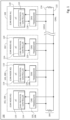
- FIG. 1 schematically illustrates an example of a CAN system 100.
- the CAN system may comprise several CAN devices 102 and a CAN bus 104.
- Each of the CAN devices 102 can be connected to the CAN bus 104.
- the CAN devices 102 are able to communicate among each other via the CAN bus 104.
- a CAN device 102 may also be referred to as a CAN node.
- a CAN device 102 may be at least a part of an electronic control units (ECUs), as an engine control module (ECM), a power train control module (PCM), an airbag module, an antilock brakes module, a cruise control module, an electric power steering module, an audio module, a window module, a door module, a mirror adjustment module, a battery module, in particular a battery management module, a recharging module for hybrid/electric cars, and/or other.
- ECUs electronice control units
- a CAN protocol may enable a communication via the CAN bus 104.
- the CAN protocol may enable communications between at least two CAN devices 102.
- each CAN device 102 includes a CAN transceiver 120 and a microcontroller 110 having an embedded CAN controller 114.
- the CAN controller 114 may be referred to as a controller or a CAN protocol controller.
- the CAN transceiver 120 may be referred to as a transceiver.
- the microcontroller 110 may be connected to at least one further device (not shown) such as a sensor, an actuator, or some other control device.
- the microcontroller 110 may be programmed to determine the meaning of a received message and/or to generate an appropriate outgoing message.
- the microcontroller 110 which may also be referred to as host processor, host or digital signal processor (DSPs).
- DSPs digital signal processor
- the microcontroller 110 may support application software that interacts with the CAN controller 108.
- the CAN bus 104 is preferably configured to carry an analog differential signal, in particular a differential voltage signal representing a CAN frame.
- the CAN bus 104 may comprise a first signal line 124, which is referred to as a first CAN signal line 124 and/or a CAN high (CANH) bus line 124.
- the CAN bus 104 may also comprise a second signal line 126, which is referred to as a second CAN signal line 126 and/or as the CAN low (CANL) bus line 126.
- the CAN transceiver 120 may comprise a transmit data, TXD, interface 128.
- the TXD interface 128 of the CAN transceiver 120 may also be referred to as a first TXD interface 128.
- the CAN transceiver 120 may further comprise a receive data, RXD, interface 130.
- the RXD interface 130 of the CAN transceiver 120 may also be referred to as a first RXD interface 130.
- the CAN transceiver 120 may comprise a further interface 220. This further interface 220 may also be referred to as a first wake-up interface 220.
- the CAN transceiver 120 may comprise a further interface 224.
- the further interface 224 may also be referred to as a first control interface 224.
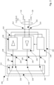
- the first TXD interface 128 of the CAN transceiver 120 is coupled to the second TXD interface 216 of the CAN controller 114 via a signal connection 228.
- the CAN controller 114 may be configured to generate a signal, referred to as a TXD signal, at the second TXD interface 210 that represents a CAN frame.
- a CAN frame comprises a plurality of bits.
- the CAN transceiver 120 comprises another interface 132, referred to as the bus interface 132.
- the bus interface 132 comprises a first bus terminal 212 and a second bus terminal 214.
- the first bus terminal 212 is configured to be connected to the first CAN bus line 124.
- the second bus terminal 214 is configured to be connected to the second CAN bus line 126.
- the CAN transceiver 120 comprises a transmitter unit 138.
- the transmitter unit 138 may be coupled to the first TXD interface 128. Via the first TXD interface 128, the transmitter unit 138 may receive the TXD signal representing a CAN frame.
- the transmitter unit 138 may further be coupled to the bus interface 132.
- the transmitter unit 138 may be configured to generate a bus signal at the CAN BUS interface 132 based on the received CAN frame, such that the bus signal represents the CAN frame.
- the bus signal is preferably a differential voltage signal.
- the corresponding voltage difference refers to a difference between the voltage at the first bus terminal 212 and the voltage at the second bus terminal 214.
- the CAN transceiver 120 comprises a receiver unit 136.
- the receiver unit 136 may be coupled to the CAN BUS interface 132.
- the receiver unit 136 can receive a bus signal 142 via the CAN BUS interface 132.
- the bus signal 142 may also be referred to as CAN bus signal 142.
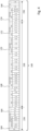
- Figure 3 schematically illustrates an example of a bus signal 142.
- the bus signal 142 may be generated by another CAN device 102 and transmitted to the CAN BUS interface 132 of the CAN transceiver 120 (of Figure 2 ) via the CAN bus 104.
- the CAN bus signal 142 may represent the CAN frame 148 shown schematically and exemplarily in Figure 3 .
- the CAN frame 148 is also referred to as the first CAN frame 148.
- the receiver unit 136 of the CAN transceiver 120 may be coupled to the first RXD interface 130.
- the first RXD interface 130 may be coupled to the second RXD interface 218 of the CAN controller 114 via a signal connection 230.
- the receiver unit 136 may be configured to generate an RXD signal at the first RXD interface 130 based on the first CAN frame 148 such that the RXD signal represents the first CAN frame 148.
- the RXD signal may be transmitted from the first RXD interface 130 to the second RXD interface 218 of the CAN controller 114 via the signal connection 230.
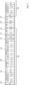
- Figure 4 schematically illustrates an example of the first CAN frame 148.
- the first CAN frame 148 shown in Figure 4 may be a CAN frame according to the CAN XL protocol.
- the first CAN frame 148 may comprise, for example: a start-of-frame, SOF, bit 164, an arbitration field 166, a control field 168, a data field 170, a cycle redundancy check, CRC, field 172, an acknowledge, ACK, field 174, and an end-of-frame, EOF, field 146. Further details on the structural design of a CAN frame according to the CAN XL protocol can be taken from the associated standard.
- the bits of the first CAN frame 148 may be transmitted at two different bit frequencies 236, 238.
- the bit frequency in particular one of the bit frequencies 236, 238, may relate to and/or be the reciprocal of the time (length) of a bit.
- the SOF bit 164 and the bits of the arbitration field 166 may be transmitted at a first bit frequency 236.
- the bits of the control field 168, the bits of the data field 170, and the bits of the CRC field 172 may be transmitted at a second bit frequency 238.
- the second bit frequency 238 is preferably greater than the first bit frequency 236.
- the first bit frequency 236 may correspond to the bit frequency for transmitting bits of a CAN frame according to the classic CAN protocol.
- the bits of the ACK field 174 and the bits of the EOF field 146 may be transmitted at the first bit frequency 236.
- the EOF field 146 comprises seven bits.
- the seven bits of the EOF field 146 are basically each recessive bits.
- Figure 5 schematically illustrates another example of the first CAN frame 148.
- the first CAN frame 148 shown in Figure 5 may be a CAN frame 148 according to the Classical CAN protocol.
- the first CAN frame 148 may comprise, for example: a SOF bit 164, an arbitration field 166, a control field 168, a data field 170, a CRC field 172, an ACK field 174, and an EOF field 146. Further details on the structural design of a CAN frame 148 according to the classical CAN protocol can be obtained from the associated standard.
- the bits of the first CAN frame 148 may be transmitted at the first bit frequency 236.
- the EOF field 146 comprises seven bits. The seven bits of the EOF field 146 are basically each recessive bits.
- intermission, ITM bits directly follow the EOF field 146.
- the ITM bits may form the so-called ITM field 150.
- the ITM field 150 comprises three bits.
- the three bits of the ITM field 150 are basically each recessive bits.
- the ITM field 150 does not form part of the first CAN frame 148.
- an interframe frame space, IFS, field 176 directly adjoins the ITM field 150.
- the IFS field 176 can represent an idle phase.
- the IFS field 176 may comprise any number N of bits, each of which is basically a recessive bit. In particular, the IFS field 176 does not form part of the first CAN frame 148.
- a further, first CAN frame 149 adjoins the IFS field 176.
- the further, first CAN frame 149 is only partially and schematically shown in Figure 5 .
- the further, first CAN frame 149 may be configured analogously to the first CAN frame 148.
- a CAN system 100 is shown schematically in Figure 1 .
- the CAN system 100 may comprise a plurality of CAN devices 102. Each CAN device 102 may be coupled to the CAN bus 104.
- the CAN controller 114 and/or the microcontroller 110 of a CAN device 102 may change from an active operating state to a deactivated state, also referred to as a sleep state. In the sleep state, the CAN controller 114 and/or the microcontroller 110 of the CAN device 102 consumes less electrical energy than in the active operating state.
- the CAN controller 114 and/or the microcontroller 110 may be woken up by the CAN transceiver 120 of the associated CAN device 102.
- the wake-up may be performed via a wake-up signal.
- one of the CAN devices 102 of the CAN system 100 may be configured to generate a CAN bus signal representing a CAN frame 148 on the CAN bus 104.
- the CAN transceivers 120 of the other CAN devices 102 may receive the CAN frame 148 represented by the bus signal.
- each CAN transceiver 102 it would be possible for each CAN transceiver 102 to send a wake-up signal to the CAN controller 114 and/or microcontroller 110 of the associated CAN device 102 in response to the received CAN frame 148 to cause a change from the sleep state to the active operating state, respectively.
- a first section 162 of the bus signal 142 representing a pattern 178 referred to as a reference pattern 178 of a predefined sequence of bits may be detected by each CAN transceiver 120.
- each CAN transceiver 120 may transmit the wake-up signal to the CAN controller 114 and/or microcontroller 110 of the respective associated CAN device 102.
- the SOF bit 164 and the bits of the arbitration field 166 are used not for the dedicated purpose only but also for the purpose of the reference pattern 178.
- the wake-up pulse 152 may be integrated into the silent section 144 of the bus signal 142 in such a way that the wake-up pulse 152 is not evaluated by the receiver unit 136 of the CAN transceiver 120 as a representation of a dominant bit. In the silent section 144, only recessive bits should be represented by the bus signal 142.
- the receiver unit 136 of the CAN transceiver 120 in the silent section 144 exclusively checks whether the differential voltage of the silent section 144 of the bus signal 142 is less than a second threshold voltage TH2.
- the second threshold voltage TH2 may be between 0.5 V and 0.9 V. In an example, the second threshold voltage TH2 is 0.7 V.
- the receiver unit 136 of the CAN transceiver 120 may detect the silent section 144 of the bus signal 142 as a plurality of recessive bits (of the EOF field 146 and/or the ITM field 150) even if at least one wake-up pulse 152 is included in the silent section 144 of the bus signal 142.
- the at least one wake-up pulse 152 in the silent section 144 of the bus signal 142 may be not visible to the receiver unit 136 of the CAN transceiver 120.
- the wake-up pulse 152 may be detected only by a particular group of CAN transceivers 120, each comprising a wake-up unit 140.
- FIG. 2 schematically illustrates an example of a CAN transceiver 120, wherein the CAN transceiver 120 comprises the TXD interface 128, the RXD interface 130, the bus interface 132, the transmitter unit 138 and the receiver unit 136.
- the bus interface 132 is configured to receive a first differential voltage signal, referred to as the bus signal 142, from the CAN bus 104 via the bus interface 132.
- the CAN transceiver 120 further comprises a wake-up unit 140.
- the wake-up unit 140 is preferably coupled to the bus interface 132. In an example, the wake-up unit 140 may receive the bus signal 142 via the bus interface 132.
- the wake-up unit 140 is configured to detect the silent section 144 of the bus signal 144.
- the silent section 144 of the bus signal 142 represents the EOF field 146 of the first CAN frame 148 and/or the ITM field 150 directly following the EOF field 146.
- the wake-up unit 140 is configured to detect, in the silent section 144 of the bus signal 142, at least one wake-up pulse 152 comprising a differential bus voltage Vw1 that is less than a first predefined negative threshold voltage TH1.
- the first threshold voltage TH1 may be between -0.2 V and -0.45 V. In an example, the first threshold voltage TH1 is -0.4 V.
- the wake-up unit 140 is configured to cause a wake-up signal to be sent in response to the at least one detected wake-up pulse 152.
- the wake-up signal may represent a wake-up command.
- the wake-up command may be used to wake up the CAN controller 114 and/or the microcontroller 110.
- the wake-up unit 140 may send the wake-up signal via a further interface 220 of the CAN transceiver 120.
- the further interface 220 may be referred to as the first wake-up interface 220.
- the wake-up unit 140 may be configured to send the wake-up signal via the RXD interface 130 of the CAN transceiver 120.
- Figure 7 schematically illustrates a corresponding embodiment of the CAN transceiver 120. In the following, reference is again made to the example in Figure 2 , wherein the explanations relating to Figure 2 may apply analogously to the example in Figure 7 , and vice versa.
- the wake-up unit 140 detects the silent section 144 of the bus signal. If the wake-up unit 140 detects at least one wake-up pulse 152 in the silent section 144, then the wake-up unit 140 will directly or indirectly send or cause to sent a wake-up signal in response to the detection of the at least one wake-up pulse 152.
- the wake-up signal is used to wake up the CAN controller 114 and/or microcontroller 110, particularly if the CAN transceiver 120 and the wake-up CAN controller 114 and/or the microcontroller 110 belong to the same CAN device 102.
- a selected group of CAN devices 102 from a larger group comprising a plurality of CAN devices 102 may each comprise the wake-up unit 140.
- the selected group of CAN devices 102 may form a partial network via the CAN bus 104 whose CAN controllers 114 and/or microcontrollers 110 may be woken up as a result of the at least one wake-up pulse 152 incorporated in the silent section 144 of the bus signal.
- the at least one wake-up pulse 152 integrated in the silent section 144 may be invisible.
- a single wake-up pulse 152 may be understood to be an embodiment of a wake-up pattern 160.
- the wake-up pattern 160 comprises at least one wake-up pulse 152 or multiple wake-up pulses 152.
- Figure 3 schematically illustrates a wake-up pattern 160, which in an example may be referred to as the first wake-up pattern 194.
- the first wake-up pattern 194 may comprise exactly two wake-up pulses 152.
- Each of the two wake-up pulses 152 may be integrated into the silent section 144 of the bus signal 142, which silent section 144 represents the EOF field 146 and/or the ITM field 150.
- the first wake-up pattern 194 may also be designed differently, in particular comprising more or less wake-up pulses 152.
- FIG. 6 schematically illustrates a further example of the bus signal 142.
- the bus signal 142 in Figure 6 differs from the bus signal 142 in Figure 3 in that a different wake-up pattern 160 is integrated into the silent section 144 of the bus signal 142.
- the wake-up pattern 160 of Figure 6 may be an example of a second wake-up pattern 196.
- the second wake-up pattern 196 may comprise, for example, exactly four wake-up pulses 152.
- the bus signal 142 of Figure 3 may represent the first CAN frame 148.
- the CAN frame 148 may be a CAN frame according to the CAN XL protocol.
- An example of such a first CAN frame 148 is shown schematically in Figure 4 .
- the bits of the data field 170 are represented by different pulses 240, 242, which are formed by the bus signal 142.
- the pulse 240 may also be referred to as the first data pulse 240.
- the pulse 242 may also be referred to as the second data pulse 242.
- the differential bus voltage of the first data pulse 240 may at least approximately correspond to the differential bus voltage Vw1 of the wake-up pulse 252, and/or vice versa.
- the differential bus voltage of the second data pulse 242 may be greater than the fourth threshold voltage TH4.
- the fourth threshold voltage TH4 is between -0.1 V and 0.1 V.
- the fourth threshold voltage TH4 may be 0 V.
- the wake-up unit 140 will not detect or evaluate the first data pulse 240 as a wake-up pulse 142.
- the wake-up unit 140 is configured to detect the at least one wake-up pulse 152 exclusively in the silent section 144 of the bus signal 142. Therefore, only the silent section 144 of the bus signal 142 is considered for the wake-up unit 140 in order to detect for the at least one wake-up pulse 142.
- the wake-up unit 140 will therefore not search for a wake-up pulse 152 in the data field 170 and will not be able to detect a wake-up pulse 152 in the data field 170.
- the wake-up unit 140 may be configured to exclusively monitor the silent section 144 of the bus signal 142 for the at least one wake-up pulse 142. As an effect, the wake-up unit 140 may robustly detect the at least one wake-up pulse 152.
- the differential bus voltage VW 1 of the wake-up pulse 152 may be approximately equal to the differential bus voltage of the first data pulse 240.
- the differential bus voltage of the first data pulse 240 is selected such that as little electromagnetic interference as possible is caused on the CAN bus 104.
- the same advantage also applies to the wake-up pulse 152, which also causes a low electromagnetic interference on the CAN bus 104.
- the differential bus voltage VW1 of the wake-up pulse 152 is between the first threshold voltage TH1 and a third predefined negative threshold voltage TH3.
- the third threshold voltage TH3 may be between -0.8 V and -2 V. Due to the voltage range between the first threshold voltage TH1 and the third threshold voltage TH3 for the differential bus voltage VW 1 of the wake-up pulse 152, it may be achieved in an example that no excessive electromagnetic interference is caused on the CAN bus 104.
- Integration of at least one wake-up pulse 152 into the silent section 144 of the bus signal 142 may be understood to mean, in particular, that the silent section 144 of the bus signal 142 forms the at least one wake-up pulse 152.
- the integration of the at least one wake-up pulse 152 into the silent section 144 of the bus signal 142 can be realized in an example without disadvantages for the data transmission rate.
- the integration of the at least one wake-up pulse 152 into the silent section 144 prevents a potential collision with other frames and/or bus signals.
- the wake-up unit 140 is configured to cause the wake-up signal in response to detecting the at least one detected wake-up pulse 152.
- the wake-up unit 140 may be coupled to the first wake-up interface 220 such that the wake-up unit 140 may send the wake-up signal via the first wake-up interface 220.
- the first wake-up interface 220 may be coupled to the second wake-up interface 222 of the CAN controller 114.
- the first wake-up interface 220 may be coupled to, for example, a power supply unit of the CAN device 102 such that the power supply unit is controllable by the wake-up unit 140 via the wake-up signal.
- the power supply unit of the device 102 may supply an electrical voltage to the microcontroller 110 and/or the CAN controller 114 in response to receiving the wake-up signal. By supplying the electrical voltage, the microcontroller 110 and/or the CAN controller 114 may change from a deactivated state to an activated state.
- the transceiver 120 in an example, is configured to change from an activated (operational) state to a (deactivated) sleep state.
- the transceiver 120 may also change from the sleep state back to the activated operational state.
- the transceiver 120 may be fully functional in the operational state.
- the transceiver 120 may have individual subunits deactivated in the sleep state. By deactivating a subunit of the transceiver 120, less electrical energy is consumed by the transceiver 120.
- the receiver unit 136 and/or the transmitter unit 138 may be deactivated. By deactivating the receiver unit 136, a consumption of electrical energy of the transceiver 120 is reduced.
- the receiver unit 136 By deactivating the transmitter unit 138, the consumption of electrical energy of the transceiver 120 can also be reduced.
- the receiver unit 136, the transmitter unit 138 and, in particular, other units of the transceiver 120 may be deactivated. This can further improve the saving of electrical energy during the sleep state.
- the receiver unit 136 By deactivating the receiver unit 136, the receiver unit 136 is not capable of generating a signal at the first RXD interface 130 that is used to wake up the CAN controller 114.
- the receiver unit 136 and/or the transmitter unit 138 of the transceiver 120 are, in particular, only activated when the transceiver 120 is in an operational state.
- the transceiver 120 is configured such that the wake-up unit 140 is activated in the sleep state of the transceiver 120.
- the wake-up unit 140 may, for example, perform the steps previously explained, such as detecting a silent section 144 of the bus signal 142, detecting a wake-up pulse 152 in the silent section 144, and/or causing a wake-up signal in response to detecting a wake-up pulse 152.
- the wake-up unit 140 which is active during the sleep state of the transceiver 120, offers the advantage that the wake-up unit 140 can directly or indirectly wake up the CAN controller 114 and/or the microcontroller 110 via the wake-up command represented by the wake-up signal.
- the wake-up unit 140 may be operational active even if the receiver unit 136 and/or the transmitter unit 138 are deactivated in the sleep state of the transceiver 120.
- the wake-up unit 140 may be used to monitor the bus signal 142 with respect to a wake-up pulse 152 in a silent section 144 and cause the CAN controller 114 and/or the microcontroller 110 to wake up if necessary.
- the wake-up unit 140 may be configured such that the active wake-up unit 140 consumes less electrical power than an activated receiver unit 136 and/or an activated transmitter unit 138.
- transceiver 120 is in a sleep state while the receiver unit 136 and/or the transmitter unit 138 are deactivated, electrical power may be saved despite the activated wake-up unit 140 without waiving the ability to wake up the CAN controller 114 and/or the microcontroller 110.
- the wake-up unit 140 may be coupled to the receiver unit 136 and/or the transmitter unit 138.
- the wake-up unit 140 may be configured to directly or indirectly control the receiver unit 136 and/or the transmitter unit 138 in response to detecting a wake-up pulse 152 such that the receiver unit 136 and/or the transmitter unit 138 are activated.
- the wake-up unit 140 may be coupled to the receiver unit 136 and/or the transmitter unit 138 such that the wake-up unit 140 may send an activation signal to the receiver unit 136 and/or the transmitter unit 138 representing a command to activate.
- the receiver unit 136 and/or the transmitter unit 138 may each be configured to activate in response to receiving the activation signal.
- the transceiver 120 may comprise a main unit 210, wherein the main unit 210 comprises the receiver unit 136 and/or the transmitter unit 138.
- the main unit 210 may be activated or deactivated.
- the wake-up unit 140 may be coupled to the main unit 210 such as to transmit the activation signal to the main unit 210.
- the main unit 210 may be configured to supply the receiver unit 136 and/or the transmitter unit 138 with an operating voltage in response to receiving the activation signal. By supplying the operating voltage, the receiver unit 136 and/or the transmitter unit 138 may be activated.
- Figure 3 schematically illustrates an example of the bus signal 142.
- a first CAN frame 148 is shown schematically in Figure 3 .
- Sections of the bus signal 142 may be assigned to one or more fields of the first CAN frame 148 by means of several vertical dashed lines.
- the corresponding sections of the bus signal can represent the bits of the respective assigned fields.
- the bus signal is only shown schematically in Figure 3 , and in particular not all parts of the bus signal 142 are shown in Figure 3 .
- the silent section 144 of the bus signal may represent either only a combination of the EOF field 146 and the ITM field 150, or only the EOF field 146 or only the ITM field 150.
- the silent section 144 of the bus signal 142 could represent only the EOF field 146 or only the ITM field 150.
- Figure 3 schematically illustrates another example in which the silent section 144 of the bus signal 142 only represents the combination of the EOF field 146 and the ITM field 150 directly following the EOF field 146.
- the EOF field 146 may comprise 7 bits, in particular exactly 7 bits, of the first CAN frame 148.
- the ITM field 150 may comprise 3 bits, in particular exactly 3 bits.
- the ITM field 150 can follow directly to the EOF field 146.
- the ITM field 180 does not form part of the first CAN frame 148.
- a so-called interframe space, IFS, 176 may directly adjoin the ITM field 150.
- the interframe space 176 may extend from the ITM field 150 to a further first CAN frame 149.
- the interframe space 176 may be represented by the bus signal 142.
- the bus voltage of the bus signal 142 may be at least substantially 0 V.
- the interframe space 176 comprises one recessive bit or more recessive bits.
- the silent section 144 of the bus signal 142 represents the EOF field 146, the ITM field 150 following the EOF field 146, and/or the interframe space 176 following the ITM field 150.
- the silent section 144 of the bus signal 142 may directly follow the trigger pulse 154 of the bus signal 142.
- the trigger pulse voltage VG of the trigger pulse 154 is preferably greater than the second threshold voltage TH2.
- the bus voltage in the silent section 144 of the bus signal 142 is always less than the second threshold voltage TH2.
- the bus voltage of the base section 156 of the bus signal 142 may be at least substantially 0 V.
- the base section 156 may be followed directly by an observation section 158 of the bus signal 142.
- the base section 156 and the subsequent observation section 158 may each form part of the silent section 144 of the bus signal 142.
- the silent section 144 of the bus signal 142 is formed from the base section 156 and the subsequent observation section 158.
- the silent section 144 may further comprise the section of the bus signal 142 during the waiting time TW.
- FIG 8 schematically illustrates an example of a flowchart for the transceiver 120.
- the transceiver 120 if in the sleep state, may provide that the receiver unit 136 and/or the transmitter unit 138 are deactivated.
- the wake-up unit 140 may be active.
- the wake-up unit 140 may be coupled to the bus interface 132 so that the bus signal 142 may be received by the wake-up unit 140 via the bus interface 132.
- the wake-up unit 140 may be configured to detect, based on the bus signal 142, a trigger pulse 154 comprising a differential bus voltage VG of the bus signal 142 that is greater than the second threshold voltage TH2.
- the trigger pulse 154 may, for example, comprise a time duration of at least 0.5 ⁇ s to 5 ⁇ s.
- the second threshold voltage TH2 is a predefined, positive threshold voltage. In an example, the second threshold voltage TH2 may be between +0.5 V and +0.9 V. In an example, the second threshold voltage TH2 may be +0.9V.
- the example of the bus signal 142 from Figure 3 schematically shows that the bus signal 142 can theoretically comprise a plurality of trigger pulses 154.
- the trigger pulse 154 can therefore not be used alone to robustly detect a subsequent silent section 144.
- the detection of the trigger pulse 154 may be followed by the waiting time TW.
- the wake-up unit 140 may be configured to wait for the waiting time TW, which follows the trigger pulse 154.
- the waiting time TW may be a predefined time. In an example, the waiting time TW may be between 0.01 ⁇ s and 2 ⁇ s, in particular between 0.1 ⁇ s and 1.3 ⁇ s.
- oscillations of the bus signal 142 can occur, which can be ignored by the wake-up unit 140, in particular if the oscillations relate to undershoots. Ignoring the possible oscillations of the bus signal 142 during the waiting time TW improves the robustness for detecting a wake-up pulse 152.
- a check may be performed to determine whether the waiting time TW is followed by a base section 156 of the bus signal 142.
- the wake-up unit 140 may be configured to detect the base section 156 of the bus signal 142 based on the bus signal 142.
- the base section 156 comprises a differential bus voltage that is between the first threshold voltage TH1 and the second threshold voltage TH2 during a predefined base time TA.
- the base time TA directly follows the waiting time TW. If a base section 156 actually follows the waiting time TW, then the differential bus voltage of the base section 156 is neither less than the first threshold voltage TH1 nor greater than the second threshold voltage TH2.
- the base section 156 lasts for the predefined base time TA.
- the base time TA may be between 2 ⁇ s and 7 ⁇ s.
- the base time TA may be predefined in relation to the bit frequency 236 used to transmit the SOF bit 164, the bits of the arbitration field 166, the bits of the ACK field 174, and/or the bits of the EOF field 146.
- the base time TA may be two to seven times a cycle time according to the aforementioned bit frequency 236.
- the bits of the data field 170 may be represented by first data pulses 240 of the bus signal 142 and second data pulses 242 of the bus signal 142.
- a so-called stuffing bit is performed at the latest after ten equal (either first or second) data pulses 240, 242.
- ten consecutive second data pulses 242 are followed by a first data pulse 240, which in this example represents the stuffing bit.
- the time TP of the ten consecutive second data pulses 242 is ten times the simple cycle time according to the second bit frequency 238. In an example, the time TP may be about 1.25 ⁇ s.
- a first data pulse 240 is generated at the latest after 1.25 ⁇ s during the transmission of the bits of the data field 170, wherein the differential bus voltage of the first data pulse 240 is less than the first threshold voltage TH1.
- the predefined base time TA should be considered again.
- the base section 156 of the bus signal 142 comprises a differential bus voltage that is neither less than the first threshold voltage TH1 nor greater than the second threshold voltage TH2.
- the base time TA may, for example, be between 2 ⁇ s and 7 ⁇ s.
- it may be determined that no transmission of bits of the data field 170 is performed during the base time TA.
- no trigger pulse 154, no wake-up pulse 152, no first data pulse 240, and also no second data pulse 242 can occur in the base section 156 that lasts a base time TA.
- a potential observation section 158 of the bus signal 142 that may follow the base section 156 of the bus signal 142 may not serve to represent bits of the data field 170.
- a check may be performed to determine whether an observation section 158 follows the base section 156. In the event that the wake-up unit 140 has not detected the base section 156, the wake-up unit 140 may abort the check.
- the wake-up unit 140 is configured to detect the observation section 158 based on the bus signal 142.
- the observation section 158 comprises a differential bus voltage that is less than the second threshold voltage TH2 during a predefined observation time T0.
- the observation time T0 directly follows the base time TA. If an observation section 158 actually follows the base section 156, then the differential bus voltage of the observation section 158 is always less than the second threshold voltage TH2.
- the observation time T0 may be between 5 ⁇ s and 7 ⁇ s.
- the observation time T0 may be predefined in relation to the first bit frequency 236 used to transmit the SOF bit 164, the bits of the arbitration field 166, the bits of the ACK field 174, and/or the bits of the EOF field 146.
- the observation time T0 may be five to seven times a cycle time according to the first bit frequency 236.
- the base time TA and the observation time T0 in total may be eleven times the cycle time of the first bit frequency 236.
- the bus signal 142 comprises a differential bus voltage that is always less than the second threshold voltage TH2.
- the base section 156 and the observation section 158 may form the silent section 144.
- the silent section 144 may further comprise the section of the bus signal 142 during the waiting period TW.
- the silent section 144 may represent the EOF field 146 and/or the ITM field 150.
- a wake-up pulse 152 which may be included in the observation section 158 of the bus signal 142, is invisible to known transceivers 120 and/or to the receiver unit 136. However, this invisibility does not apply to the wake-up unit 140.
- the wake-up unit 140 is configured to detect the at least one wake-up pulse 152 in the observation section 158 of the bus signal 142.
- Each wake-up pulse 152 comprises a differential bus voltage that is less than the first threshold voltage TH1.
- Each wake-up pulse 152 may comprise a time between 0.01 ⁇ s and 10 ⁇ s.
- each wake-up pulse 152 comprises a time that is less than the cycle time of the first bit frequency 236, a plurality of wake-up pulses 152 may be included in the observation section 158.
- each wake-up pulse 152 may comprise a time that is between 0.05 ⁇ s and 5 ⁇ s, in particular between 0.05 ⁇ s and 3 ⁇ s.
- the wake-up signal may be caused, in particular generated, by the wake-up unit 140.
- the wake-up unit 140 may terminate the check.
- the wake-up unit 140 is configured to detect a predefined wake-up pattern 160 in the silent section 144, in particular in the observation section 158.
- the wake-up pattern 160 may be the first wake-up pattern 194 as schematically illustrated in Figure 3 .
- the wake-up pattern 160 may be the second wake-up pattern 196 as schematically illustrated in Figure 6 .
- the wake-up pattern 160 may comprise a plurality of wake-up pulses 152.
- the wake-up pattern 160 may comprise at least two, three, five or ten wake-up pulses 152.
- each wake-up pulse 152 of the wake-up pattern 160 reference may be made to the preceding explanations, preferred features, technical effects, and advantages in an analogous manner as previously described for the wake-up pulse 152.
- each wake-up pulse 152 of the wake-up pattern 160 comprises a differential bus voltage VW1 that is less than the first threshold voltage TH1.
- the plurality of wake-up pulses 152 of the wake-up pattern 160 may each be separated by a signal section 224 of the bus signal 142, referred to as a separation section 224, in which the differential bus voltage is greater than the first threshold voltage TH1 and less than the second threshold voltage TH2.
- the differential bus voltage of each separation section 224 may be approximately 0 V.
- the wake-up pulses 152 of the wake-up pattern 160 are not arranged in direct succession.
- Each separation section 224 may also form a part of the wake-up pattern 160.
- the wake-up pattern 160 is formed of a plurality of wake-up pulses 152 and a plurality of separation sections 244.
- the wake-up unit 140 may be configured to cause the wake-up signal in response to detecting the at least one wake-up pulse 152.
- the wake-up unit 140 is configured such that a single wake-up pulse 152 is not sufficient to cause the wake-up signal.
- the wake-up unit 140 may be configured to cause the wake-up signal to be sent via an interface of the transceiver 120 in response to detection of the wake-up pattern 160.
- the wake-up unit 140 may be coupled to the first wake-up interface 220. In this case, the wake-up unit 140 may generate and send the wake-up signal via the first wake-up interface 220. In another example, the wake-up unit 140 may be coupled to the RXD interface 130.
- Figure 7 schematically illustrates an example of the transceiver 120 wherein the wake-up unit 140 is coupled to the RXD interface 130. In this case, the wake-up unit 140 may generate and send the wake-up signal via the RXD interface 130. In another example, the wake-up unit 140 may be directly or indirectly coupled to the receiver unit 136.
- the wake-up unit 140 may control the receiver unit 136 such that the wake-up signal is sent from the receiver unit 136 via the RXD interface 130. As a result, the wake-up unit 140 causes the receiver unit 136 to send the wake-up signal. However, the sending is caused by the controlling of the receiver unit 136 by the wake-up unit 140.
- the receiver unit 136 may be configured to detect the SOF bit 164, a bit of the arbitration field 166, a bit of the ACK field 174, a bit of the EOF field 146 solely on whether the bus voltage of the bus signal 142 representing the respective bit is either greater than the second threshold voltage TH2 or less than the second threshold voltage TH2. If the bus voltage is greater than the second threshold voltage TH2, then the receiver unit 136 evaluates the bus voltage as a representation of a dominant bit. If the bus voltage is less than the second threshold voltage TH2, then the receiver unit 136 evaluates the bus voltage as a representation of a recessive bit.
- a wake-up pulse 152 which is integrated into the silent section 144 of the bus signal 142, comprises a bus voltage that is less than the first threshold voltage TH1.
- the first threshold voltage TH1 is less than the second threshold voltage TH2.
- the silent section 144 may represent at least a section of the EOF field 146. If the wake-up pulse 152 occurs while the bus signal 142 represents at least a section of the EOF field 146, then the receiver unit 136 will determine that the bus voltage of the bus signal is less than the second threshold voltage TH2. As an effect, the receiver unit 136 will evaluate the wake-up pulse 152 as a representation of a recessive bit.
- the integration of the at least one wake-up pulse 152 into the silent section 144 of the bus signal 142 remains invisible to the receiver unit 136.
- the preceding explanations apply in particular if the silent section 144 of the bus signal 142 is received by a receiver unit 136 that is activated rather than deactivated. If the receiver unit 136 is deactivated, then it may be provided that the receiver unit 136 does not evaluate the silent section 144 of the bus signal 142.
- the receiver unit 136 may be configured, if the receiver unit 136 is activated, to generate an RXD signal at the first RXD interface 130 based on the bus signal 142 representing the first CAN frame 148, such that the RXD signal represents the first CAN frame 148.
- the wake-up unit 140 may be configured to control the receiver unit 136 such that a wake-up pulse 152 incorporated in a silent section 144 of the bus signal 142 representing the EOF field 146 is evaluated as a recessive bit by the receiver unit 136 and/or is represented as a recessive bit by the RXD signal. As an effect, this may prevent the at least one wake-up pulse 152 from resulting in an error signal at the RXD interface 130 and/or at the bus interface 132.
- the wake-up unit 140 may be configured to detect a first section 162 of the bus signal 142 representing the SOF bit 164 and/or the arbitration field 166.
- the wake-up unit 140 may be configured to detect a predefined reference pattern 178 represented by the first section 162 of the bus signal 142.
- the reference pattern 178 is not to be confused with and different to the previously explained wake-up pattern 152.
- the reference pattern 178 does not comprise a voltage that is less than the first threshold voltage TH1. Detecting the reference pattern 178 may be used as a prerequisite to start the check for the wake-up pattern 152, for example according to the flowchart of Figure 8 .
- the wake-up unit 140 may therefore be configured to perform the detection of the wake-up pulse 152 and/or the causing of the wake-up signal only if the reference pattern 178 has been detected beforehand. This can improve the robustness for detecting the wake-up pattern 152 against possible interference signals on the CAN bus 104.
- the wake-up unit 140 is configured to cause the wake-up signal to be sent via an interface, in particular the first wake-up interface 220, in response to the detection of at least one wake-up pulse 152.
- the first wake-up interface 220 may be coupled to a second wake-up interface 222 of the CAN controller 114.
- the CAN controller 114 may be configured to change from the inactive state to the active operational state in response to the received wake-up signal.
- a CAN device 102 as also schematically illustrated in Figure 2 , comprises the CAN transceiver 120 and the CAN controller 114.
- the CAN device 102 may comprise the microcontroller 110, wherein the CAN controller 114 may be implemented by the microcontroller 110.
- FIG. 1 schematically illustrates an example of a CAN system 100.
- the system 100 may comprise a plurality of CAN devices 102 coupled via a CAN bus 104.
- One of the CAN devices 102 may cause a bus signal 142 on the CAN bus 104.
- the bus signal 142 may be received by the other CAN devices 102.
- one of the CAN devices 102 receiving the bus signal 142 comprises a CAN transceiver 120 including a wake-up unit 140
- the CAN controller 114 of the same CAN device 102 may be woken up by a wake-up signal caused by the wake-up unit 140.
- this requires that at least one wake-up pulse 152 is integrated into a silent section 144 of the bus signal 142.
- the CAN transceiver 120 of the CAN device 102 which causes the bus signal 142 on the CAN bus 104, should therefore have the ability to integrate the at least one wake-up pulse 152 in the silent section 144 of the bus signal 142.
- a CAN transceiver 120 may have the ability to integrate the wake-up pulse 152 into the silent section 144 of the bus signal 142.
- the CAN transceiver 120 may be configured to receive a control command via an interface of the CAN transceiver 120 other than the bus interface 132.
- the control command may indicate the sending of the wake-up pulse 152 and/or the integration of the wake-up pulse 152 into the bus signal 142.
- the CAN transceiver 120 may be activated if the transmitter unit 138 and/or the receiver unit 136 are activated.
- the other interface of the CAN transceiver 120 may be referred to as the first control interface 224.
- the first control interface 224 may be other than the first TXD interface 128 and/or the first RXD interface 130 and/or first wake-up interface 220.
- the first control interface 224 may be coupled to a second control interface 226 via a signal connection.
- the CAN controller 114 may be configured to generate the control command.
- the CAN controller 114 may send a control signal from the second control interface 226 to the first control interface 224, wherein the control signal represents the control command.
- the CAN transceiver 120 may, in an example, be configured to receive, via the first TXD interface 128, a TXD signal representing a CAN frame. This CAN frame is to be referred to as the second CAN frame. The TXD signal and/or the second CAN frame do not represent the at least one wake-up pulse 158.
- the CAN transceiver 120 may be configured to generate a bus signal 142 at the CAN BUS interface 132 such that the bus signal 142 represents the second CAN frame.
- the CAN transceiver 120 adapts the bus signal 142 such that a silent section 144 of the bus signal 142 representing the EOF field 146 of the second CAN frame and/or a directly following the ITM field comprises at least one wake-up pulse 152.
- the bus signal 142 is transmitted from the other CAN transceiver 120 to the CAN transceivers 120 of the other CAN devices 102 via the CAN bus 104. If at least one of the CAN transceivers 120 receiving the bus signal 142 comprises a wake-up unit 140, the corresponding wake-up unit 140 may detect the wake-up pulse 152.
- the CAN transceiver 120 receiving the bus signal 142 may be considered to receive the bus signal 142 representing the first CAN frame 148. In this case, the second CAN frame can correspond to the first CAN frame.
- the different wake-up patterns 194, 196 may be used to form different partial networks in a CAN system 100.
- FIG. 1 schematically illustrates an example of a CAN system 100.
- the CAN system 100 comprises a plurality of CAN devices 102.
- Each CAN device 102 comprises a CAN transceiver 120.
- One CAN transceiver 120 of the plurality of CAN transceivers 120 may be referred to as a first CAN transceiver 186.
- Another CAN transceiver 120 of the plurality of CAN transceivers 120 may be referred to as a second CAN transceiver 188.
- a CAN device 102 comprising the first CAN transceiver 186 may be referred to as a first CAN device 198.
- a CAN device 102 comprising the second CAN transceiver 188 may be referred to as a second CAN device 200.
- the wake-up unit 140 of the first CAN transceiver 186 is configured to be capable of detecting a first wake-up pattern 194 as the wake-up pattern 160.
- the wake-up unit 140 of the first CAN transceiver 186 may further be configured to not detect the second wake-up pattern 196 as a wake-up pattern 160, and/or to be able to exclusively detect the first wake-up pattern 194 as a wake-up pattern 160.
- the wake-up unit 140 of the second CAN transceiver 188 is configured to be able to detect a second wake-up pattern 196 as a wake-up pattern 160.
- the second wake-up pattern 196 is different from the first wake-up pattern 194.
- the wake-up unit 140 of the second CAN transceiver 188 may further be configured to not detect the first wake-up pattern 194 as a wake-up pattern 160 and/or to be able to exclusively detect the second wake-up pattern 196 as a wake-up pattern 160.
- the CAN system 100 may comprise the CAN bus 104, at least one first CAN transceiver 186, and at least one second CAN transceiver 188.
- the CAN system 100 may comprise the CAN bus 104, at least one first CAN device 198 comprising the first CAN transceiver 186, and at least one second CAN device 200 comprising the second CAN transceiver 188.
- the CAN system 100 may preferably comprise a plurality of first CAN devices 198 and a plurality of second CAN devices 200.
- the plurality of first CAN devices 198 may form a first partial network via the CAN bus 104.
- the plurality of second CAN devices 200 may form a second partial network via the CAN bus 104.
- Figure 9 schematically illustrates an example of a flowchart for a method 202.
- the method 202 is for the CAN transceiver 120.
- the method 202 may comprise the following steps:
- the systems and methods described herein may at least partially be embodied by a computer program or a plurality of computer programs, which may exist in a variety of forms both active and inactive in a single computer system or across multiple computer systems.
- they may exist as software program(s) comprised of program instructions in source code, object code, executable code or other formats for performing some of the steps.
- Any of the above may be embodied on a computer-readable medium, which may include storage devices and signals, in compressed or uncompressed form.
- the term "computer” refers to any electronic device comprising a processor, such as a general-purpose central processing unit (CPU), a specific-purpose processor or a microcontroller.
- a computer is capable of receiving data (an input), of performing a sequence of predetermined operations thereupon, and of producing thereby a result in the form of information or signals (an output).
- the term "computer” will mean either a processor in particular or more generally a processor in association with an assemblage of interrelated elements contained within a single case or housing.
- processor or “processing unit” refers to a data processing circuit that may be a microcontroller, a co-processor, a microcontroller, a microcomputer, a central processing unit, a field programmable gate array (FPGA), a programmable logic circuit, and/or any circuit that manipulates signals (analog or digital) based on operational instructions that are stored in a memory.
- memory refers to a storage circuit or multiple storage circuits such as read-only memory, random access memory, volatile memory, non-volatile memory, static memory, dynamic memory, Flash memory, cache memory, and/or any circuit that stores digital information.
- a "computer-readable medium” or “storage medium” may be any means that can contain, store, communicate, propagate, or transport a computer program for use by or in connection with the instruction execution system, apparatus, or device.
- the computer-readable medium may be, for example but not limited to, an electronic, magnetic, optical, electromagnetic, infrared, or semiconductor system, apparatus, device, or propagation medium.
- the computer-readable medium may include the following: an electrical connection having one or more wires, a portable computer diskette, a random-access memory (RAM), a read-only memory (ROM), an erasable programmable read-only memory (EPROM or Flash memory), an optical fiber, a portable compact disc read-only memory (CDROM), a digital versatile disc (DVD), a Blu-ray disc (BD), and a memory card.
- RAM random-access memory
- ROM read-only memory
- EPROM or Flash memory erasable programmable read-only memory
- CDROM compact disc read-only memory
- DVD digital versatile disc
- BD Blu-ray disc
Landscapes
- Engineering & Computer Science (AREA)
- Computer Networks & Wireless Communication (AREA)
- Signal Processing (AREA)
- Small-Scale Networks (AREA)
Abstract
The present invention relates to a Controller Area Network, CAN, transceiver, comprising: a transmit data, TXD, interface, a receive data, RXD, interface, a bus interface for coupling to a CAN bus, a receiver unit, a transmitter unit, and a wake-up unit, wherein the bus interface is configured to receive a first differential voltage signal, referred to as the bus signal, from the CAN bus via the bus interface, wherein the wake-up unit is configured to detect a silent section of the bus signal representing an end-of-frame, EOF, field of a first CAN frame and/or an inter-mission-space, ITM, following to the EOF field based on the bus signal, wherein the wake-up unit is configured to detect in the silent section of the bus signal at least one wake-up pulse having a differential bus voltage that is less than a first predefined negative threshold voltage (TH1), and wherein the wake-up unit is configured to cause a wake-up signal representing a wake-up instruction to be sent via an interface of the transceiver, in particular the RXD interface or another interface of the transceiver, in response to the at least one detected wake-up pulse. The present invention also relates to a CAN device, a CAN system and a method for the CAN transceiver.
Description
- The present disclosure relates to a CAN transceiver, a CAN device, a CAN system, and a method for the CAN transceiver.
- A Controller Area Network (CAN) can be used for communications within vehicles, in particular within automobiles. It will be appreciated that CAN also has application outside of the field of automobiles. A CAN bus system may include multiple CAN devices, so called as nodes or electronic control units (ECUs), such as an engine control module (ECM), a power train control module (PCM), airbags, antilock brakes, cruise control, electric power steering, audio systems, windows, doors, mirror adjustment, battery and recharging systems for hybrid/electric cars, and many more. Several nodes may be connected to a joint CAN bus, such that the nodes can communicate among each other over the CAN bus using a CAN protocol. The CAN protocol is used to enable communications between the various nodes. The data link layer of the CAN protocol is standardized as International Standards Organization (ISO) 11898-1:2003. CAN Flexible Data-Rate or "CAN FD" is an extension of the standardized CAN data link layer protocol and is integrated into the ISO 11898-1:2015 standard. CAN FD may provide higher data rates. The standardized CAN data link layer protocol is being further extended to provide even higher data rates. A further extension, referred to as CAN XL, with an optional level scheme on the physical layer allowing even higher data rates, is in the definition phase discussed under CiA610 (CAN in Automation) and is moving towards standardization in the form of ISO11898-1:202x.
- This summary is provided to introduce a selection of concepts in a simplified form that are further described below in the detailed description. This summary is not intended to identify key features or essential features of the claimed subject matter, nor is it intended to be used to limit the scope of the claimed subject matter.
- Aspects of the disclosure are defined in the accompanying claims.
- In accordance with a first aspect of the present disclosure, a Controller Area Network, CAN, transceiver is provided. The CAN transceiver comprising: a transmit data, TXD, interface, a receive data, RXD, interface, a bus interface for coupling to a CAN bus, a receiver unit, a transmitter unit, and a wake-up unit, wherein the bus interface is configured to receive a first differential voltage signal, referred to as the bus signal, from the CAN bus via the bus interface, wherein the wake-up unit is configured to detect a silent section of the bus signal representing an end-of-frame, EOF, field of a first CAN frame and/or an inter-mission-space, ITM, following to the EOF field based on the bus signal, wherein the wake-up unit is configured to detect in the silent section of the bus signal at least one wake-up pulse having a differential bus voltage that is less than a first predefined negative threshold voltage, and wherein the wake-up unit is configured to cause a wake-up signal representing a wake-up instruction to be sent via an interface of the transceiver, in particular the RXD interface or another interface of the transceiver, in response to the at least one detected wake-up pulse.
- In one or more embodiments, the wake-up unit is configured to detect, based on the bus signal, a trigger pulse having a differential bus voltage that is greater than a positive, predefined second threshold voltage, wherein the wake-up unit is configured to wait for a predefined waiting time, that follows the trigger pulse, wherein the wake-up unit is configured to detect, based on the bus signal, a base section of the bus signal, wherein the base section having a differential bus voltage between the first threshold voltage and the second threshold voltage during a predefined base time following the waiting time, wherein the wake-up unit is configured to detect, based on the bus signal, an observation section of the bus signal, wherein the observation section having a differential bus voltage that is less than the second threshold voltage during a predefined observation time following the base time, wherein the observation section forms at least a part of the silent section, and wherein the wake-up unit is configured to detect in the observation section of the bus signal at least one wake-up pulse having a differential bus voltage that is less than the first threshold voltage.
- In one or more embodiments, the waiting time is between 0.01 µs and 2 µs, in particular between 0.1 µs and 1.3 µs, and/or wherein the base time is between 2 and 7 times a cycle time according to a predefined bit frequency at the bus interface, and/or wherein the observation time is between 5 and 7 times the cycle time according to the predefined bit frequency at the bus interface.
- In one or more embodiments, the second threshold voltage is between plus 0.5 volts and plus 0.9 volts.
- In one or more embodiments, the first threshold voltage is between minus 0.25 volts and minus 0.45 volts.
- In one or more embodiments, the wake-up unit is configured to detect in the silent section a predefined wake-up pattern comprising a plurality of wake-up pulses each having a differential bus voltage that is less than the first predefined negative threshold voltage, and wherein the wake-up unit is configured to cause the wake-up signal representing a wake-up instruction to be sent, in particular via the RXD interface or another interface of the transceiver, in response to the detected wake-up pattern.
- In one or more embodiments, the wake-up unit is coupled to the receiver unit and/or the RXD interface to cause the sending of the wake-up signal.
- In one or more embodiments, the CAN transceiver and/or the receiver unit is configured to treat a wake-up pulse as a recessive bit.
- In one or more embodiments, the wake-up unit is configured to control the receiver unit such that the receiver unit generates a signal at the RXD interface representing a recessive bit based on the wake-up pulse.
- In one or more embodiments, the wake-up unit is configured to detect a first section of the bus signal representing at least one of the Start-of-frame field, SOF, the arbitration field, and/or the control field of the first CAN frame, wherein the wake-up unit is configured to detect another pattern, referred to as reference pattern, being represented by the first section of the bus signal, and wherein the wake-up unit is configured to cause the wake-up signal only if and/or after the reference pattern was detected.
- In one or more embodiments, the CAN transceiver, if being activated, is configured to receive, via an interface of the transceiver other than the bus interface, a control instruction to send out a wake-up pattern, wherein the CAN transceiver is configured to receive another CAN frame, referred to as second CAN frame, via the TXD interface, and wherein the CAN transceiver is configured to transmit an output signal via the bus interface, such that the output signal represents the second CAN frame with the exception that an instruction section of the output signal representing the EOF and/or the ITM of the CAN frame further comprises at least one wake-up pulse having a differential bus voltage less than the first threshold voltage.
- According to a second aspect of the present disclosure, a CAN device is provided. The CAN device comprising: a CAN transceiver according to the first aspect and/or any corresponding embodiment, and a CAN controller, wherein the CAN controller is coupled to the TXD interface of the CAN transceiver and the RXD interface of the CAN transceiver, wherein the wake-up unit of the CAN transceiver is configured, in response to the detected wake-up pulse or the detected wake-up pattern, to cause the wake-up signal to be sent to the CAN controller via the RXD interface or another interface of the CAN transceiver, and wherein the CAN controller is configured to change from an inactive state to an operating state in response to the received wake-up signal.
- According to a third aspect of the present disclosure, a CAN system is provided. The CAN system comprising: a CAN bus, a first CAN transceiver according to first aspect and/or any corresponding embodiment, and a second CAN transceiver according to first aspect and/or any corresponding embodiment, wherein the wake-up unit of the first CAN transceiver is configured to detect as a wake-up pattern a first wake-up pattern, wherein the wake-up unit of the second CAN transceiver is configured to detect as another wake-up pattern a second wake-up pattern, and wherein the first and second wake-up patterns are different.
- In one or more embodiment, the CAN system comprising: a first CAN device according to the second aspect, a second CAN device according to the second aspect, wherein the first CAN device comprises as transceiver the first transceiver, and wherein the second CAN device comprises as transceiver the second transceiver.
- According to a fourth aspect of the present disclosure, a method for a CAN transceiver comprising a transmit data, TXD, interface, a receive data, RXD, interface, a bus interface for coupling to a CAN bus, a receiver unit, a transmitter unit, and a wake-up unit is provided. The method comprises the steps of: (a) receiving a first differential voltage signal, referred to as the bus signal at the bus interface, (b) the wake-up unit detecting a silent section of the bus signal representing an end-of-frame, EOF, field of a CAN frame and/or an inter-mission-space, ITM, following to the EOF field based on the bus signal, (c) the wake-up unit detecting in the silent second of the bus signal at least one wake-up pulse having a differential bus voltage that is less than a first predefined negative threshold voltage (TH1), and (d) the wake-up unit causing a wake-up signal representing a wake-up instruction to be sent via an interface of the transceiver, in particular the RXD interface or another interface of the transceiver, in response to the at least one detected wake-up pulse.
- In accordance with a fifth aspect of the present disclosure, a computer program is provided, comprising executable instructions which, when executed by a processing unit of the transceiver, cause the processing unit being configured to carry out the method of the fourth aspect and/or one or more embodiments thereof.
- Embodiments of the present disclosure will be described in more detail with reference to the appended drawings. It is to be noted, however, that the appended drawings illustrate only typical embodiments of the present disclosure and are therefore not to be considered limiting of its scope, such that other equally effective embodiments may be implemented. Advantages of the subject matter claimed will become apparent to those skilled in the art upon reading this description in conjunction with the accompanying drawings, in which like reference numerals have been used to designate like elements, and in which:
-
Figure 1 shows an embodiment of a simplified block diagram of a CAN system. -
Figure 2 shows an embodiment of a simplified block diagram of a CAN device. -
Figure 3 shows an embodiment of a waveform. -
Figure 4 shows an embodiment of a simplified CAN XL frame. -
Figure 5 shows an embodiment of a simplified CAN frame. -
Figure 6 shows another embodiment of a simplified waveform. -
Figure 7 shows another embodiment of a simplified block diagram of a CAN device. -
Figure 8 shows an embodiment of a simplified flow chart. -
Figure 9 shows an embodiment of a simplified method flow chart. - As indicated in the background section of the present disclosure, a Controller Area Network (CAN) can be used for communications, in particular within vehicles. It will be appreciated that CAN communication also has application outside of the field of vehicles.
-
Figure 1 schematically illustrates an example of aCAN system 100. The CAN system may compriseseveral CAN devices 102 and aCAN bus 104. Each of theCAN devices 102 can be connected to theCAN bus 104. As a result, the CANdevices 102 are able to communicate among each other via the CANbus 104. ACAN device 102 may also be referred to as a CAN node. In an example, aCAN device 102 may be at least a part of an electronic control units (ECUs), as an engine control module (ECM), a power train control module (PCM), an airbag module, an antilock brakes module, a cruise control module, an electric power steering module, an audio module, a window module, a door module, a mirror adjustment module, a battery module, in particular a battery management module, a recharging module for hybrid/electric cars, and/or other. - A CAN protocol may enable a communication via the CAN
bus 104. For example, the CAN protocol may enable communications between at least twoCAN devices 102. In an example, eachCAN device 102 includes aCAN transceiver 120 and amicrocontroller 110 having an embeddedCAN controller 114. The CANcontroller 114 may be referred to as a controller or a CAN protocol controller. TheCAN transceiver 120 may be referred to as a transceiver. - The
microcontroller 110 may be connected to at least one further device (not shown) such as a sensor, an actuator, or some other control device. Themicrocontroller 110 may be programmed to determine the meaning of a received message and/or to generate an appropriate outgoing message. Themicrocontroller 110, which may also be referred to as host processor, host or digital signal processor (DSPs). In an example, themicrocontroller 110 may support application software that interacts with the CAN controller 108. - The
CAN bus 104 is preferably configured to carry an analog differential signal, in particular a differential voltage signal representing a CAN frame. TheCAN bus 104 may comprise afirst signal line 124, which is referred to as a firstCAN signal line 124 and/or a CAN high (CANH)bus line 124. TheCAN bus 104 may also comprise asecond signal line 126, which is referred to as a secondCAN signal line 126 and/or as the CAN low (CANL)bus line 126. -
Figure 2 schematically illustrates an example of aCAN device 102. TheCAN device 102 comprises theCAN transceiver 120 and theCAN controller 114. In an example, theCAN device 102 comprises themicrocontroller 110 comprising theCAN controller 114. If advantageous explanations, preferred features, technical effects and/or advantages are presented in the following with respect to theCAN device 102, these may apply in an analogous manner to theCAN transceiver 120. - The
CAN transceiver 120 may comprise a transmit data, TXD,interface 128. TheTXD interface 128 of theCAN transceiver 120 may also be referred to as afirst TXD interface 128. TheCAN transceiver 120 may further comprise a receive data, RXD,interface 130. TheRXD interface 130 of theCAN transceiver 120 may also be referred to as afirst RXD interface 130. TheCAN transceiver 120 may comprise afurther interface 220. Thisfurther interface 220 may also be referred to as a first wake-upinterface 220. TheCAN transceiver 120 may comprise afurther interface 224. Thefurther interface 224 may also be referred to as afirst control interface 224. - The
CAN controller 114 may comprise aTXD interface 216, which may be referred to as asecond TXD interface 216. In addition, theCAN controller 114 may comprise anRXD interface 218, which is referred to as asecond RXD interface 218. In an example, theCAN controller 114 may comprise anotherinterface 222, referred to as a second wake-upinterface 222. TheCAN controller 114 may comprise anotherinterface 226, referred to as thesecond control interface 226. - In an example, the
first TXD interface 128 of theCAN transceiver 120 is coupled to thesecond TXD interface 216 of theCAN controller 114 via asignal connection 228. In an example, theCAN controller 114 may be configured to generate a signal, referred to as a TXD signal, at thesecond TXD interface 210 that represents a CAN frame. A CAN frame comprises a plurality of bits. - The
CAN transceiver 120 comprises anotherinterface 132, referred to as thebus interface 132. In an example, thebus interface 132 comprises afirst bus terminal 212 and asecond bus terminal 214. Thefirst bus terminal 212 is configured to be connected to the firstCAN bus line 124. Thesecond bus terminal 214 is configured to be connected to the secondCAN bus line 126. - The
CAN transceiver 120 comprises atransmitter unit 138. Thetransmitter unit 138 may be coupled to thefirst TXD interface 128. Via thefirst TXD interface 128, thetransmitter unit 138 may receive the TXD signal representing a CAN frame. Thetransmitter unit 138 may further be coupled to thebus interface 132. Thetransmitter unit 138 may be configured to generate a bus signal at theCAN BUS interface 132 based on the received CAN frame, such that the bus signal represents the CAN frame. The bus signal is preferably a differential voltage signal. The corresponding voltage difference refers to a difference between the voltage at thefirst bus terminal 212 and the voltage at thesecond bus terminal 214. - The
CAN transceiver 120 comprises areceiver unit 136. Thereceiver unit 136 may be coupled to theCAN BUS interface 132. Thereceiver unit 136 can receive abus signal 142 via theCAN BUS interface 132. Thebus signal 142 may also be referred to asCAN bus signal 142.Figure 3 schematically illustrates an example of abus signal 142. Thebus signal 142 may be generated by anotherCAN device 102 and transmitted to theCAN BUS interface 132 of the CAN transceiver 120 (ofFigure 2 ) via theCAN bus 104. In an example, theCAN bus signal 142 may represent theCAN frame 148 shown schematically and exemplarily inFigure 3 . TheCAN frame 148 is also referred to as thefirst CAN frame 148. - The
receiver unit 136 of theCAN transceiver 120 may be coupled to thefirst RXD interface 130. Thefirst RXD interface 130 may be coupled to thesecond RXD interface 218 of theCAN controller 114 via asignal connection 230. In an example, thereceiver unit 136 may be configured to generate an RXD signal at thefirst RXD interface 130 based on thefirst CAN frame 148 such that the RXD signal represents thefirst CAN frame 148. The RXD signal may be transmitted from thefirst RXD interface 130 to thesecond RXD interface 218 of theCAN controller 114 via thesignal connection 230. -
Figure 4 schematically illustrates an example of thefirst CAN frame 148. Thefirst CAN frame 148 shown inFigure 4 may be a CAN frame according to the CAN XL protocol. Thefirst CAN frame 148 may comprise, for example: a start-of-frame, SOF,bit 164, anarbitration field 166, acontrol field 168, adata field 170, a cycle redundancy check, CRC,field 172, an acknowledge, ACK,field 174, and an end-of-frame, EOF,field 146. Further details on the structural design of a CAN frame according to the CAN XL protocol can be taken from the associated standard. - If the
first CAN frame 148 is configured according to the CAN XL protocol, the bits of thefirst CAN frame 148 may be transmitted at twodifferent bit frequencies bit frequencies SOF bit 164 and the bits of thearbitration field 166 may be transmitted at afirst bit frequency 236. The bits of thecontrol field 168, the bits of thedata field 170, and the bits of theCRC field 172 may be transmitted at asecond bit frequency 238. Thesecond bit frequency 238 is preferably greater than thefirst bit frequency 236. Thefirst bit frequency 236 may correspond to the bit frequency for transmitting bits of a CAN frame according to the classic CAN protocol. In an example, the bits of theACK field 174 and the bits of theEOF field 146 may be transmitted at thefirst bit frequency 236. As can be seen fromFigure 4 , theEOF field 146 comprises seven bits. The seven bits of theEOF field 146 are basically each recessive bits. -
Figure 5 schematically illustrates another example of thefirst CAN frame 148. Thefirst CAN frame 148 shown inFigure 5 may be aCAN frame 148 according to the Classical CAN protocol. Also in this embodiment, thefirst CAN frame 148 may comprise, for example: aSOF bit 164, anarbitration field 166, acontrol field 168, adata field 170, aCRC field 172, anACK field 174, and anEOF field 146. Further details on the structural design of aCAN frame 148 according to the classical CAN protocol can be obtained from the associated standard. If thefirst CAN frame 148 is configured according to the Classical CAN protocol, the bits of thefirst CAN frame 148 may be transmitted at thefirst bit frequency 236. As can be seen fromFigure 5 , theEOF field 146 comprises seven bits. The seven bits of theEOF field 146 are basically each recessive bits. - In the example shown in
Figure 5 , intermission, ITM, bits directly follow theEOF field 146. The ITM bits may form the so-calledITM field 150. In an example, theITM field 150 comprises three bits. The three bits of theITM field 150 are basically each recessive bits. In particular, theITM field 150 does not form part of thefirst CAN frame 148. - In the example shown in
Figure 5 , an interframe frame space, IFS,field 176 directly adjoins theITM field 150. TheIFS field 176 can represent an idle phase. TheIFS field 176 may comprise any number N of bits, each of which is basically a recessive bit. In particular, theIFS field 176 does not form part of thefirst CAN frame 148. - In the example shown in
Figure 5 , a further,first CAN frame 149 adjoins theIFS field 176. The further,first CAN frame 149 is only partially and schematically shown inFigure 5 . The further,first CAN frame 149 may be configured analogously to thefirst CAN frame 148. - A
CAN system 100 is shown schematically inFigure 1 . TheCAN system 100 may comprise a plurality ofCAN devices 102. EachCAN device 102 may be coupled to theCAN bus 104. In order to save electrical energy, theCAN controller 114 and/or themicrocontroller 110 of aCAN device 102 may change from an active operating state to a deactivated state, also referred to as a sleep state. In the sleep state, theCAN controller 114 and/or themicrocontroller 110 of theCAN device 102 consumes less electrical energy than in the active operating state. In order to change from the sleep state back to the active operating state, theCAN controller 114 and/or themicrocontroller 110 may be woken up by theCAN transceiver 120 of the associatedCAN device 102. The wake-up may be performed via a wake-up signal. - In an example, one of the
CAN devices 102 of theCAN system 100 may be configured to generate a CAN bus signal representing aCAN frame 148 on theCAN bus 104. TheCAN transceivers 120 of theother CAN devices 102 may receive theCAN frame 148 represented by the bus signal. In principle, it would be possible for each CAN transceiver 102 to send a wake-up signal to theCAN controller 114 and/ormicrocontroller 110 of the associatedCAN device 102 in response to the received CAN frame 148 to cause a change from the sleep state to the active operating state, respectively. In an example, afirst section 162 of thebus signal 142 representing apattern 178 referred to as areference pattern 178 of a predefined sequence of bits may be detected by eachCAN transceiver 120. In response to the detection of thereference pattern 178, each CAN transceiver 120 may transmit the wake-up signal to theCAN controller 114 and/ormicrocontroller 110 of the respective associated CANdevice 102. - By using the bits represented in the
first section 162 at the beginning of a CAN frame, it may turn out that theSOF bit 164 and the bits of thearbitration field 166 are used not for the dedicated purpose only but also for the purpose of thereference pattern 178. - It may be desirable not to wake up all CAN
controllers 114 ormicrocontrollers 110 of all CANdevices 102, but to wake up only a predetermined group ofCAN controllers 114 or microcontrollers 110 (of respective associated devices 102). In other words, it may be desirable to be able to specifically wake up a partial group of theCAN devices 102 or associated CANcontrollers 114 ormicrocontrollers 110. - As can be deduced from the following explanations, it is possible to integrate at least one wake-up
pulse 152 in asilent section 144 of thebus signal 142, wherein thesilent section 144 of thebus signal 142 represents theEOF field 146 and/or theITM field 150. The wake-uppulse 152 may be integrated into thesilent section 144 of thebus signal 142 in such a way that the wake-uppulse 152 is not evaluated by thereceiver unit 136 of theCAN transceiver 120 as a representation of a dominant bit. In thesilent section 144, only recessive bits should be represented by thebus signal 142. In simplified terms, thereceiver unit 136 of theCAN transceiver 120 in thesilent section 144 exclusively checks whether the differential voltage of thesilent section 144 of thebus signal 142 is less than a second threshold voltage TH2. The second threshold voltage TH2 may be between 0.5 V and 0.9 V. In an example, the second threshold voltage TH2 is 0.7 V. In an example, if the differential voltage of thesilent section 144 of thebus signal 142 is less than the second threshold voltage TH2, then thereceiver unit 136 of theCAN transceiver 120 may detect thesilent section 144 of thebus signal 142 as a plurality of recessive bits (of theEOF field 146 and/or the ITM field 150) even if at least one wake-uppulse 152 is included in thesilent section 144 of thebus signal 142. As an effect, the at least one wake-uppulse 152 in thesilent section 144 of thebus signal 142 may be not visible to thereceiver unit 136 of theCAN transceiver 120. The wake-uppulse 152 may be detected only by a particular group ofCAN transceivers 120, each comprising a wake-upunit 140. -
Figure 2 schematically illustrates an example of aCAN transceiver 120, wherein theCAN transceiver 120 comprises theTXD interface 128, theRXD interface 130, thebus interface 132, thetransmitter unit 138 and thereceiver unit 136. Thebus interface 132 is configured to receive a first differential voltage signal, referred to as thebus signal 142, from theCAN bus 104 via thebus interface 132. TheCAN transceiver 120 further comprises a wake-upunit 140. The wake-upunit 140 is preferably coupled to thebus interface 132. In an example, the wake-upunit 140 may receive thebus signal 142 via thebus interface 132. The wake-upunit 140 is configured to detect thesilent section 144 of thebus signal 144. Thesilent section 144 of thebus signal 142 represents theEOF field 146 of thefirst CAN frame 148 and/or theITM field 150 directly following theEOF field 146. - The wake-up
unit 140 is configured to detect, in thesilent section 144 of thebus signal 142, at least one wake-uppulse 152 comprising a differential bus voltage Vw1 that is less than a first predefined negative threshold voltage TH1. The first threshold voltage TH1 may be between -0.2 V and -0.45 V. In an example, the first threshold voltage TH1 is -0.4 V. The wake-upunit 140 is configured to cause a wake-up signal to be sent in response to the at least one detected wake-uppulse 152. The wake-up signal may represent a wake-up command. The wake-up command may be used to wake up theCAN controller 114 and/or themicrocontroller 110. In an example, the wake-upunit 140 may send the wake-up signal via afurther interface 220 of theCAN transceiver 120. Thefurther interface 220 may be referred to as the first wake-upinterface 220. In another example, the wake-upunit 140 may be configured to send the wake-up signal via theRXD interface 130 of theCAN transceiver 120.Figure 7 schematically illustrates a corresponding embodiment of theCAN transceiver 120. In the following, reference is again made to the example inFigure 2 , wherein the explanations relating toFigure 2 may apply analogously to the example inFigure 7 , and vice versa. - Against the background of the preceding explanations, it may be summarized in simplified terms that the wake-up
unit 140 detects thesilent section 144 of the bus signal. If the wake-upunit 140 detects at least one wake-uppulse 152 in thesilent section 144, then the wake-upunit 140 will directly or indirectly send or cause to sent a wake-up signal in response to the detection of the at least one wake-uppulse 152. The wake-up signal is used to wake up theCAN controller 114 and/ormicrocontroller 110, particularly if theCAN transceiver 120 and the wake-upCAN controller 114 and/or themicrocontroller 110 belong to thesame CAN device 102. In an example, a selected group ofCAN devices 102 from a larger group comprising a plurality ofCAN devices 102 may each comprise the wake-upunit 140. As an effect, the selected group ofCAN devices 102 may form a partial network via theCAN bus 104 whose CANcontrollers 114 and/ormicrocontrollers 110 may be woken up as a result of the at least one wake-uppulse 152 incorporated in thesilent section 144 of the bus signal. For theother CAN devices 102 whose CANtransceivers 120 do not comprise the previously explained wake-upunit 140, the at least one wake-uppulse 152 integrated in thesilent section 144 may be invisible. - In an example, a single wake-up
pulse 152 may be understood to be an embodiment of a wake-uppattern 160. In another example, it may be understood that the wake-uppattern 160 comprises at least one wake-uppulse 152 or multiple wake-uppulses 152.Figure 3 schematically illustrates a wake-uppattern 160, which in an example may be referred to as the first wake-uppattern 194. The first wake-uppattern 194 may comprise exactly two wake-uppulses 152. Each of the two wake-uppulses 152 may be integrated into thesilent section 144 of thebus signal 142, whichsilent section 144 represents theEOF field 146 and/or theITM field 150. In principle, the first wake-uppattern 194 may also be designed differently, in particular comprising more or less wake-uppulses 152. -
Figure 6 schematically illustrates a further example of thebus signal 142. Thebus signal 142 inFigure 6 differs from thebus signal 142 inFigure 3 in that a different wake-uppattern 160 is integrated into thesilent section 144 of thebus signal 142. The wake-uppattern 160 ofFigure 6 may be an example of a second wake-uppattern 196. The second wake-uppattern 196 may comprise, for example, exactly four wake-uppulses 152. - In an example, the
bus signal 142 ofFigure 3 may represent thefirst CAN frame 148. In an example, theCAN frame 148 may be a CAN frame according to the CAN XL protocol. An example of such afirst CAN frame 148 is shown schematically inFigure 4 . The bits of thedata field 170 are represented bydifferent pulses bus signal 142. Thepulse 240 may also be referred to as thefirst data pulse 240. Thepulse 242 may also be referred to as thesecond data pulse 242. In an example, the differential bus voltage of thefirst data pulse 240 may at least approximately correspond to the differential bus voltage Vw1 of the wake-up pulse 252, and/or vice versa. The differential bus voltage of thesecond data pulse 242 may be greater than the fourth threshold voltage TH4. In an example, the fourth threshold voltage TH4 is between -0.1 V and 0.1 V. For example, the fourth threshold voltage TH4 may be 0 V. - Although the differential bus voltage of the
first data pulse 240 may be approximately equal to the differential bus voltage VW1 of the wake-uppulse 152, the wake-upunit 140 will not detect or evaluate thefirst data pulse 240 as a wake-uppulse 142. In an example, the wake-upunit 140 is configured to detect the at least one wake-uppulse 152 exclusively in thesilent section 144 of thebus signal 142. Therefore, only thesilent section 144 of thebus signal 142 is considered for the wake-upunit 140 in order to detect for the at least one wake-uppulse 142. In particular, the wake-upunit 140 will therefore not search for a wake-uppulse 152 in thedata field 170 and will not be able to detect a wake-uppulse 152 in thedata field 170. In other words, in an example, the wake-upunit 140 may be configured to exclusively monitor thesilent section 144 of thebus signal 142 for the at least one wake-uppulse 142. As an effect, the wake-upunit 140 may robustly detect the at least one wake-uppulse 152. - Previously, it was explained that the differential
bus voltage VW 1 of the wake-uppulse 152 may be approximately equal to the differential bus voltage of thefirst data pulse 240. The differential bus voltage of thefirst data pulse 240 is selected such that as little electromagnetic interference as possible is caused on theCAN bus 104. As an effect, the same advantage also applies to the wake-uppulse 152, which also causes a low electromagnetic interference on theCAN bus 104. In an example, the differential bus voltage VW1 of the wake-uppulse 152 is between the first threshold voltage TH1 and a third predefined negative threshold voltage TH3. The third threshold voltage TH3 may be between -0.8 V and -2 V. Due to the voltage range between the first threshold voltage TH1 and the third threshold voltage TH3 for the differentialbus voltage VW 1 of the wake-uppulse 152, it may be achieved in an example that no excessive electromagnetic interference is caused on theCAN bus 104. - Integration of at least one wake-up
pulse 152 into thesilent section 144 of thebus signal 142 may be understood to mean, in particular, that thesilent section 144 of thebus signal 142 forms the at least one wake-uppulse 152. - By integrating the at least one wake-up
pulse 152 into thesilent section 144 of thebus signal 142, it may be achieved as an effect and advantage that no additional bandwidth is required on theCAN bus 104 for the at least one wake-uppulse 152. Therefore, the integration of the at least one wake-up pulse into thesilent section 144 of thebus signal 142 can be realized in an example without disadvantages for the data transmission rate. As a further advantage, the integration of the at least one wake-uppulse 152 into thesilent section 144 prevents a potential collision with other frames and/or bus signals. - Previously, it was explained that the wake-up
unit 140 is configured to cause the wake-up signal in response to detecting the at least one detected wake-uppulse 152. In an example, the wake-upunit 140 may be coupled to the first wake-upinterface 220 such that the wake-upunit 140 may send the wake-up signal via the first wake-upinterface 220. In an example, the first wake-upinterface 220 may be coupled to the second wake-upinterface 222 of theCAN controller 114. In another example, the first wake-upinterface 220 may be coupled to, for example, a power supply unit of theCAN device 102 such that the power supply unit is controllable by the wake-upunit 140 via the wake-up signal. In an example, the power supply unit of thedevice 102 may supply an electrical voltage to themicrocontroller 110 and/or theCAN controller 114 in response to receiving the wake-up signal. By supplying the electrical voltage, themicrocontroller 110 and/or theCAN controller 114 may change from a deactivated state to an activated state. - The
transceiver 120, in an example, is configured to change from an activated (operational) state to a (deactivated) sleep state. Thetransceiver 120 may also change from the sleep state back to the activated operational state. Thetransceiver 120 may be fully functional in the operational state. Thetransceiver 120 may have individual subunits deactivated in the sleep state. By deactivating a subunit of thetransceiver 120, less electrical energy is consumed by thetransceiver 120. In the sleep state of thetransceiver 120, thereceiver unit 136 and/or thetransmitter unit 138 may be deactivated. By deactivating thereceiver unit 136, a consumption of electrical energy of thetransceiver 120 is reduced. By deactivating thetransmitter unit 138, the consumption of electrical energy of thetransceiver 120 can also be reduced. In the sleep state of thetransceiver 120, in an example, thereceiver unit 136, thetransmitter unit 138 and, in particular, other units of thetransceiver 120 may be deactivated. This can further improve the saving of electrical energy during the sleep state. By deactivating thereceiver unit 136, thereceiver unit 136 is not capable of generating a signal at thefirst RXD interface 130 that is used to wake up theCAN controller 114. Thereceiver unit 136 and/or thetransmitter unit 138 of thetransceiver 120 are, in particular, only activated when thetransceiver 120 is in an operational state. - In an example, the
transceiver 120 is configured such that the wake-upunit 140 is activated in the sleep state of thetransceiver 120. In the active state of the wake-upunit 140, the wake-upunit 140 may, for example, perform the steps previously explained, such as detecting asilent section 144 of thebus signal 142, detecting a wake-uppulse 152 in thesilent section 144, and/or causing a wake-up signal in response to detecting a wake-uppulse 152. The wake-upunit 140, which is active during the sleep state of thetransceiver 120, offers the advantage that the wake-upunit 140 can directly or indirectly wake up theCAN controller 114 and/or themicrocontroller 110 via the wake-up command represented by the wake-up signal. In particular, the wake-upunit 140 may be operational active even if thereceiver unit 136 and/or thetransmitter unit 138 are deactivated in the sleep state of thetransceiver 120. In other words, the wake-upunit 140 may be used to monitor thebus signal 142 with respect to a wake-uppulse 152 in asilent section 144 and cause theCAN controller 114 and/or themicrocontroller 110 to wake up if necessary. The wake-upunit 140 may be configured such that the active wake-upunit 140 consumes less electrical power than an activatedreceiver unit 136 and/or an activatedtransmitter unit 138. If thetransceiver 120 is in a sleep state while thereceiver unit 136 and/or thetransmitter unit 138 are deactivated, electrical power may be saved despite the activated wake-upunit 140 without waiving the ability to wake up theCAN controller 114 and/or themicrocontroller 110. - In an example, the wake-up
unit 140 may be coupled to thereceiver unit 136 and/or thetransmitter unit 138. The wake-upunit 140 may be configured to directly or indirectly control thereceiver unit 136 and/or thetransmitter unit 138 in response to detecting a wake-uppulse 152 such that thereceiver unit 136 and/or thetransmitter unit 138 are activated. In an example, the wake-upunit 140 may be coupled to thereceiver unit 136 and/or thetransmitter unit 138 such that the wake-upunit 140 may send an activation signal to thereceiver unit 136 and/or thetransmitter unit 138 representing a command to activate. Thereceiver unit 136 and/or thetransmitter unit 138 may each be configured to activate in response to receiving the activation signal. In an example, thetransceiver 120 may comprise amain unit 210, wherein themain unit 210 comprises thereceiver unit 136 and/or thetransmitter unit 138. In an example, themain unit 210 may be activated or deactivated. The wake-upunit 140 may be coupled to themain unit 210 such as to transmit the activation signal to themain unit 210. Themain unit 210 may be configured to supply thereceiver unit 136 and/or thetransmitter unit 138 with an operating voltage in response to receiving the activation signal. By supplying the operating voltage, thereceiver unit 136 and/or thetransmitter unit 138 may be activated. -
Figure 3 schematically illustrates an example of thebus signal 142. Below thebus signal 142, an example of afirst CAN frame 148 is shown schematically inFigure 3 . Sections of thebus signal 142 may be assigned to one or more fields of thefirst CAN frame 148 by means of several vertical dashed lines. The corresponding sections of the bus signal can represent the bits of the respective assigned fields. At this point, it should be noted once again that the bus signal is only shown schematically inFigure 3 , and in particular not all parts of thebus signal 142 are shown inFigure 3 . - In an example, the
silent section 144 of the bus signal may represent either only a combination of theEOF field 146 and theITM field 150, or only theEOF field 146 or only theITM field 150. In an example, thesilent section 144 of thebus signal 142 could represent only theEOF field 146 or only theITM field 150.Figure 3 schematically illustrates another example in which thesilent section 144 of thebus signal 142 only represents the combination of theEOF field 146 and theITM field 150 directly following theEOF field 146. TheEOF field 146 may comprise 7 bits, in particular exactly 7 bits, of thefirst CAN frame 148. TheITM field 150 may comprise 3 bits, in particular exactly 3 bits. TheITM field 150 can follow directly to theEOF field 146. In an example, the ITM field 180 does not form part of thefirst CAN frame 148. - In an example, a so-called interframe space, IFS, 176 may directly adjoin the
ITM field 150. Theinterframe space 176 may extend from theITM field 150 to a furtherfirst CAN frame 149. Theinterframe space 176 may be represented by thebus signal 142. During theinterframe space 176, the bus voltage of thebus signal 142 may be at least substantially 0 V. Against this background, it may be assumed in an example that theinterframe space 176 comprises one recessive bit or more recessive bits. In an example, thesilent section 144 of thebus signal 142 represents theEOF field 146, theITM field 150 following theEOF field 146, and/or theinterframe space 176 following theITM field 150. - As can be seen in an example from the signal waveform of the
bus signal 142 ofFig. 3 , thesilent section 144 of thebus signal 142 may directly follow thetrigger pulse 154 of thebus signal 142. The trigger pulse voltage VG of thetrigger pulse 154 is preferably greater than the second threshold voltage TH2. The bus voltage in thesilent section 144 of thebus signal 142 is always less than the second threshold voltage TH2. At the transition from thetrigger pulse 154 to thesilent section 144, there may be a brief oscillation, in particular undershoot, of the bus voltage. In an example, it should be assumed that the short-term oscillation only occurs during the waiting time TW, which directly follows thetrigger pulse 154. Abase section 156 of thebus signal 142 may directly follow after the waiting time TW. The bus voltage of thebase section 156 of thebus signal 142 may be at least substantially 0 V. Thebase section 156 may be followed directly by anobservation section 158 of thebus signal 142. Thebase section 156 and thesubsequent observation section 158 may each form part of thesilent section 144 of thebus signal 142. In an example, thesilent section 144 of thebus signal 142 is formed from thebase section 156 and thesubsequent observation section 158. In another example, thesilent section 144 may further comprise the section of thebus signal 142 during the waiting time TW. -
Figure 8 schematically illustrates an example of a flowchart for thetransceiver 120. Thetransceiver 120, if in the sleep state, may provide that thereceiver unit 136 and/or thetransmitter unit 138 are deactivated. During the sleep state of thetransceiver 120, the wake-upunit 140 may be active. The wake-upunit 140 may be coupled to thebus interface 132 so that thebus signal 142 may be received by the wake-upunit 140 via thebus interface 132. The wake-upunit 140 may be configured to detect, based on thebus signal 142, atrigger pulse 154 comprising a differential bus voltage VG of thebus signal 142 that is greater than the second threshold voltage TH2. Thetrigger pulse 154 may, for example, comprise a time duration of at least 0.5 µs to 5 µs. The second threshold voltage TH2 is a predefined, positive threshold voltage. In an example, the second threshold voltage TH2 may be between +0.5 V and +0.9 V. In an example, the second threshold voltage TH2 may be +0.9V. - The example of the
bus signal 142 fromFigure 3 schematically shows that thebus signal 142 can theoretically comprise a plurality oftrigger pulses 154. Thetrigger pulse 154 can therefore not be used alone to robustly detect a subsequentsilent section 144. Based on the example flowchart ofFigure 8 , the detection of thetrigger pulse 154 may be followed by the waiting time TW. The wake-upunit 140 may be configured to wait for the waiting time TW, which follows thetrigger pulse 154. The waiting time TW may be a predefined time. In an example, the waiting time TW may be between 0.01 µs and 2 µs, in particular between 0.1 µs and 1.3 µs. During the waiting time TW, oscillations of thebus signal 142 can occur, which can be ignored by the wake-upunit 140, in particular if the oscillations relate to undershoots. Ignoring the possible oscillations of thebus signal 142 during the waiting time TW improves the robustness for detecting a wake-uppulse 152. - Based on the example of the flowchart of
Figure 8 , after the waiting time TW has been waited, a check may be performed to determine whether the waiting time TW is followed by abase section 156 of thebus signal 142. In an example, the wake-upunit 140 may be configured to detect thebase section 156 of thebus signal 142 based on thebus signal 142. Thebase section 156 comprises a differential bus voltage that is between the first threshold voltage TH1 and the second threshold voltage TH2 during a predefined base time TA. The base time TA directly follows the waiting time TW. If abase section 156 actually follows the waiting time TW, then the differential bus voltage of thebase section 156 is neither less than the first threshold voltage TH1 nor greater than the second threshold voltage TH2. As an effect, it may be determined by the detection of thebase section 156 that neither a pulse corresponding to thetrigger pulse 154 nor a pulse corresponding to the wake-uppulse 152 has occurred in thebase section 156. Therefore, no first data pulse 240 can have occurred in thebase section 156. - The
base section 156 lasts for the predefined base time TA. In an example, the base time TA may be between 2 µs and 7 µs. In another example, the base time TA may be predefined in relation to thebit frequency 236 used to transmit theSOF bit 164, the bits of thearbitration field 166, the bits of theACK field 174, and/or the bits of theEOF field 146. In an example, the base time TA may be two to seven times a cycle time according to theaforementioned bit frequency 236. If thefirst CAN frame 148 is configured as a CAN frame according to the CAN XL standard, then the bits of thedata field 170 may be represented byfirst data pulses 240 of thebus signal 142 andsecond data pulses 242 of thebus signal 142. According to the CAN XL standard, a so-called stuffing bit is performed at the latest after ten equal (either first or second)data pulses second data pulses 242 are followed by afirst data pulse 240, which in this example represents the stuffing bit. The time TP of the ten consecutivesecond data pulses 242 is ten times the simple cycle time according to thesecond bit frequency 238. In an example, the time TP may be about 1.25 µs. As an effect, afirst data pulse 240 is generated at the latest after 1.25 µs during the transmission of the bits of thedata field 170, wherein the differential bus voltage of thefirst data pulse 240 is less than the first threshold voltage TH1. Against this background, the predefined base time TA should be considered again. During the base time TA, thebase section 156 of thebus signal 142 comprises a differential bus voltage that is neither less than the first threshold voltage TH1 nor greater than the second threshold voltage TH2. The base time TA may, for example, be between 2 µs and 7 µs. As an effect, it may be determined that no transmission of bits of thedata field 170 is performed during the base time TA. As a further effect, it may be determined that nosecond data pulse 242 occurs during the base time TA. - In the two previously paragraphs, it was determined as a result that no
trigger pulse 154, no wake-uppulse 152, nofirst data pulse 240, and also no second data pulse 242 can occur in thebase section 156 that lasts a base time TA. As another effect, it may be noted that apotential observation section 158 of thebus signal 142 that may follow thebase section 156 of thebus signal 142 may not serve to represent bits of thedata field 170. - Based on the example flowchart of
Figure 8 , after the wake-upunit 140 detects thebase section 156, a check may be performed to determine whether anobservation section 158 follows thebase section 156. In the event that the wake-upunit 140 has not detected thebase section 156, the wake-upunit 140 may abort the check. - In an example, the wake-up
unit 140 is configured to detect theobservation section 158 based on thebus signal 142. Theobservation section 158 comprises a differential bus voltage that is less than the second threshold voltage TH2 during a predefined observation time T0. The observation time T0 directly follows the base time TA. If anobservation section 158 actually follows thebase section 156, then the differential bus voltage of theobservation section 158 is always less than the second threshold voltage TH2. In an example, the observation time T0 may be between 5 µs and 7 µs. In another example, the observation time T0 may be predefined in relation to thefirst bit frequency 236 used to transmit theSOF bit 164, the bits of thearbitration field 166, the bits of theACK field 174, and/or the bits of theEOF field 146. In an example, the observation time T0 may be five to seven times a cycle time according to thefirst bit frequency 236. In another example, the base time TA and the observation time T0 in total may be eleven times the cycle time of thefirst bit frequency 236. As an effect, it may be assumed that no bits of the following fields or bits of thefirst CAN frame 148 are represented in thebase section 156 and the subsequent observation section 158:SOF 164,arbitration field 166,control field 168,data field 170,CRC field 172,ACK field 174. - During the base time TA and during the observation time T0, the
bus signal 142 comprises a differential bus voltage that is always less than the second threshold voltage TH2. Thebase section 156 and theobservation section 158 may form thesilent section 144. Thesilent section 144 may further comprise the section of thebus signal 142 during the waiting period TW. In light of the foregoing explanations, it may be noted as an effect that thesilent section 144 may represent theEOF field 146 and/or theITM field 150. A wake-uppulse 152, which may be included in theobservation section 158 of thebus signal 142, is invisible to knowntransceivers 120 and/or to thereceiver unit 136. However, this invisibility does not apply to the wake-upunit 140. The wake-upunit 140 is configured to detect the at least one wake-uppulse 152 in theobservation section 158 of thebus signal 142. Each wake-uppulse 152 comprises a differential bus voltage that is less than the first threshold voltage TH1. Each wake-uppulse 152 may comprise a time between 0.01 µs and 10 µs. In particular, if each wake-uppulse 152 comprises a time that is less than the cycle time of thefirst bit frequency 236, a plurality of wake-uppulses 152 may be included in theobservation section 158. In an example, each wake-uppulse 152 may comprise a time that is between 0.05 µs and 5 µs, in particular between 0.05 µs and 3 µs. - Based on the example of the flowchart of
Figure 8 , after the at least one wake-uppulse 152 is detected, the wake-up signal may be caused, in particular generated, by the wake-upunit 140. In the case where the wake-upunit 140 does not detect a wake-uppulse 152 in theobservation section 158, the wake-upunit 140 may terminate the check. - In an example, the wake-up
unit 140 is configured to detect a predefined wake-uppattern 160 in thesilent section 144, in particular in theobservation section 158. In an example, the wake-uppattern 160 may be the first wake-uppattern 194 as schematically illustrated inFigure 3 . In another example, the wake-uppattern 160 may be the second wake-uppattern 196 as schematically illustrated inFigure 6 . - The wake-up
pattern 160 may comprise a plurality of wake-uppulses 152. In an example, the wake-uppattern 160 may comprise at least two, three, five or ten wake-uppulses 152. For each wake-uppulse 152 of the wake-uppattern 160, reference may be made to the preceding explanations, preferred features, technical effects, and advantages in an analogous manner as previously described for the wake-uppulse 152. For example, each wake-uppulse 152 of the wake-uppattern 160 comprises a differential bus voltage VW1 that is less than the first threshold voltage TH1. The plurality of wake-uppulses 152 of the wake-uppattern 160 may each be separated by asignal section 224 of thebus signal 142, referred to as aseparation section 224, in which the differential bus voltage is greater than the first threshold voltage TH1 and less than the second threshold voltage TH2. The differential bus voltage of eachseparation section 224 may be approximately 0 V. In an example, the wake-uppulses 152 of the wake-uppattern 160 are not arranged in direct succession. Eachseparation section 224 may also form a part of the wake-uppattern 160. In an example, the wake-uppattern 160 is formed of a plurality of wake-uppulses 152 and a plurality of separation sections 244. - Previously, it was explained that the wake-up
unit 140 may be configured to cause the wake-up signal in response to detecting the at least one wake-uppulse 152. In an example, the wake-upunit 140 is configured such that a single wake-uppulse 152 is not sufficient to cause the wake-up signal. In an example, the wake-upunit 140 may be configured to cause the wake-up signal to be sent via an interface of thetransceiver 120 in response to detection of the wake-uppattern 160. - In an example, the wake-up
unit 140 may be coupled to the first wake-upinterface 220. In this case, the wake-upunit 140 may generate and send the wake-up signal via the first wake-upinterface 220. In another example, the wake-upunit 140 may be coupled to theRXD interface 130.Figure 7 schematically illustrates an example of thetransceiver 120 wherein the wake-upunit 140 is coupled to theRXD interface 130. In this case, the wake-upunit 140 may generate and send the wake-up signal via theRXD interface 130. In another example, the wake-upunit 140 may be directly or indirectly coupled to thereceiver unit 136. In an example, the wake-upunit 140 may control thereceiver unit 136 such that the wake-up signal is sent from thereceiver unit 136 via theRXD interface 130. As a result, the wake-upunit 140 causes thereceiver unit 136 to send the wake-up signal. However, the sending is caused by the controlling of thereceiver unit 136 by the wake-upunit 140. - If the
CAN transceiver 120 is configured according to the CAN XL standard, then thereceiver unit 136 may be configured to detect theSOF bit 164, a bit of thearbitration field 166, a bit of theACK field 174, a bit of theEOF field 146 solely on whether the bus voltage of thebus signal 142 representing the respective bit is either greater than the second threshold voltage TH2 or less than the second threshold voltage TH2. If the bus voltage is greater than the second threshold voltage TH2, then thereceiver unit 136 evaluates the bus voltage as a representation of a dominant bit. If the bus voltage is less than the second threshold voltage TH2, then thereceiver unit 136 evaluates the bus voltage as a representation of a recessive bit. A wake-uppulse 152, which is integrated into thesilent section 144 of thebus signal 142, comprises a bus voltage that is less than the first threshold voltage TH1. The first threshold voltage TH1 is less than the second threshold voltage TH2. Thesilent section 144 may represent at least a section of theEOF field 146. If the wake-uppulse 152 occurs while thebus signal 142 represents at least a section of theEOF field 146, then thereceiver unit 136 will determine that the bus voltage of the bus signal is less than the second threshold voltage TH2. As an effect, thereceiver unit 136 will evaluate the wake-uppulse 152 as a representation of a recessive bit. As a further effect, the integration of the at least one wake-uppulse 152 into thesilent section 144 of thebus signal 142 remains invisible to thereceiver unit 136. The preceding explanations apply in particular if thesilent section 144 of thebus signal 142 is received by areceiver unit 136 that is activated rather than deactivated. If thereceiver unit 136 is deactivated, then it may be provided that thereceiver unit 136 does not evaluate thesilent section 144 of thebus signal 142. - The
receiver unit 136 may be configured, if thereceiver unit 136 is activated, to generate an RXD signal at thefirst RXD interface 130 based on thebus signal 142 representing thefirst CAN frame 148, such that the RXD signal represents thefirst CAN frame 148. The wake-upunit 140 may be configured to control thereceiver unit 136 such that a wake-uppulse 152 incorporated in asilent section 144 of thebus signal 142 representing theEOF field 146 is evaluated as a recessive bit by thereceiver unit 136 and/or is represented as a recessive bit by the RXD signal. As an effect, this may prevent the at least one wake-uppulse 152 from resulting in an error signal at theRXD interface 130 and/or at thebus interface 132. - In another example, the wake-up
unit 140 may be configured to detect afirst section 162 of thebus signal 142 representing theSOF bit 164 and/or thearbitration field 166. In an example, the wake-upunit 140 may be configured to detect apredefined reference pattern 178 represented by thefirst section 162 of thebus signal 142. Thereference pattern 178 is not to be confused with and different to the previously explained wake-uppattern 152. Thereference pattern 178 does not comprise a voltage that is less than the first threshold voltage TH1. Detecting thereference pattern 178 may be used as a prerequisite to start the check for the wake-uppattern 152, for example according to the flowchart ofFigure 8 . The wake-upunit 140 may therefore be configured to perform the detection of the wake-uppulse 152 and/or the causing of the wake-up signal only if thereference pattern 178 has been detected beforehand. This can improve the robustness for detecting the wake-uppattern 152 against possible interference signals on theCAN bus 104. - It was previously explained that the wake-up
unit 140 is configured to cause the wake-up signal to be sent via an interface, in particular the first wake-upinterface 220, in response to the detection of at least one wake-uppulse 152. The first wake-upinterface 220 may be coupled to a second wake-upinterface 222 of theCAN controller 114. TheCAN controller 114 may be configured to change from the inactive state to the active operational state in response to the received wake-up signal. In one example, aCAN device 102, as also schematically illustrated inFigure 2 , comprises theCAN transceiver 120 and theCAN controller 114. In an example, theCAN device 102 may comprise themicrocontroller 110, wherein theCAN controller 114 may be implemented by themicrocontroller 110. -
Figure 1 schematically illustrates an example of aCAN system 100. Thesystem 100 may comprise a plurality ofCAN devices 102 coupled via aCAN bus 104. One of theCAN devices 102 may cause abus signal 142 on theCAN bus 104. Thebus signal 142 may be received by theother CAN devices 102. If one of theCAN devices 102 receiving thebus signal 142 comprises aCAN transceiver 120 including a wake-upunit 140, theCAN controller 114 of thesame CAN device 102 may be woken up by a wake-up signal caused by the wake-upunit 140. However, this requires that at least one wake-uppulse 152 is integrated into asilent section 144 of thebus signal 142. TheCAN transceiver 120 of theCAN device 102, which causes thebus signal 142 on theCAN bus 104, should therefore have the ability to integrate the at least one wake-uppulse 152 in thesilent section 144 of thebus signal 142. - Reference is made below to the aspect of how a
CAN transceiver 120 may have the ability to integrate the wake-uppulse 152 into thesilent section 144 of thebus signal 142. In an example, if theCAN transceiver 120 is activated, theCAN transceiver 120 may be configured to receive a control command via an interface of theCAN transceiver 120 other than thebus interface 132. The control command may indicate the sending of the wake-uppulse 152 and/or the integration of the wake-uppulse 152 into thebus signal 142. TheCAN transceiver 120 may be activated if thetransmitter unit 138 and/or thereceiver unit 136 are activated. The other interface of theCAN transceiver 120 may be referred to as thefirst control interface 224. Thefirst control interface 224 may be other than thefirst TXD interface 128 and/or thefirst RXD interface 130 and/or first wake-upinterface 220. Thefirst control interface 224 may be coupled to asecond control interface 226 via a signal connection. TheCAN controller 114 may be configured to generate the control command. In an example, theCAN controller 114 may send a control signal from thesecond control interface 226 to thefirst control interface 224, wherein the control signal represents the control command. - The
CAN transceiver 120 may, in an example, be configured to receive, via thefirst TXD interface 128, a TXD signal representing a CAN frame. This CAN frame is to be referred to as the second CAN frame. The TXD signal and/or the second CAN frame do not represent the at least one wake-uppulse 158. TheCAN transceiver 120 may be configured to generate abus signal 142 at theCAN BUS interface 132 such that thebus signal 142 represents the second CAN frame. However, in response to receiving the control command, theCAN transceiver 120 adapts thebus signal 142 such that asilent section 144 of thebus signal 142 representing theEOF field 146 of the second CAN frame and/or a directly following the ITM field comprises at least one wake-uppulse 152. Thebus signal 142 is transmitted from theother CAN transceiver 120 to theCAN transceivers 120 of theother CAN devices 102 via theCAN bus 104. If at least one of theCAN transceivers 120 receiving thebus signal 142 comprises a wake-upunit 140, the corresponding wake-upunit 140 may detect the wake-uppulse 152. TheCAN transceiver 120 receiving thebus signal 142 may be considered to receive thebus signal 142 representing thefirst CAN frame 148. In this case, the second CAN frame can correspond to the first CAN frame. - It has already been explained in connection with
Figures 3 and6 that several different wake-uppatterns patterns CAN system 100. -
Figure 1 schematically illustrates an example of aCAN system 100. TheCAN system 100 comprises a plurality ofCAN devices 102. EachCAN device 102 comprises aCAN transceiver 120. OneCAN transceiver 120 of the plurality ofCAN transceivers 120 may be referred to as afirst CAN transceiver 186. Another CAN transceiver 120 of the plurality ofCAN transceivers 120 may be referred to as asecond CAN transceiver 188. ACAN device 102 comprising thefirst CAN transceiver 186 may be referred to as a first CAN device 198. ACAN device 102 comprising thesecond CAN transceiver 188 may be referred to as a second CAN device 200. - In an example, the wake-up
unit 140 of thefirst CAN transceiver 186 is configured to be capable of detecting a first wake-uppattern 194 as the wake-uppattern 160. The wake-upunit 140 of thefirst CAN transceiver 186 may further be configured to not detect the second wake-uppattern 196 as a wake-uppattern 160, and/or to be able to exclusively detect the first wake-uppattern 194 as a wake-uppattern 160. - In an example, the wake-up
unit 140 of thesecond CAN transceiver 188 is configured to be able to detect a second wake-uppattern 196 as a wake-uppattern 160. The second wake-uppattern 196 is different from the first wake-uppattern 194. The wake-upunit 140 of thesecond CAN transceiver 188 may further be configured to not detect the first wake-uppattern 194 as a wake-uppattern 160 and/or to be able to exclusively detect the second wake-uppattern 196 as a wake-uppattern 160. - Against this background, the
CAN system 100 may comprise theCAN bus 104, at least onefirst CAN transceiver 186, and at least onesecond CAN transceiver 188. In another example, theCAN system 100 may comprise theCAN bus 104, at least one first CAN device 198 comprising thefirst CAN transceiver 186, and at least one second CAN device 200 comprising thesecond CAN transceiver 188. TheCAN system 100 may preferably comprise a plurality of first CAN devices 198 and a plurality of second CAN devices 200. The plurality of first CAN devices 198 may form a first partial network via theCAN bus 104. The plurality of second CAN devices 200 may form a second partial network via theCAN bus 104. -
Figure 9 schematically illustrates an example of a flowchart for amethod 202. In particular, themethod 202 is for theCAN transceiver 120. Themethod 202 may comprise the following steps: - a) receiving a first differential voltage signal, referred to as the
bus signal 142 at thebus interface 132, - b) the wake-up
unit 140 detecting asilent section 144 of thebus signal 142 representing an end-of-frame, EOF,field 146 of aCAN frame 148 and/or an intermission-space, ITM, 150 following to theEOF field 146 based on thebus signal 142, - c) the wake-up
unit 140 detecting in thesilent section 144 of thebus signal 142 at least one wake-uppulse 152 having a differential bus voltage that is less than a first predefined negative threshold voltage TH1, and - d) the wake-up
unit 140 causing a wake-up signal representing a wake-up instruction to be sent via an interface of the transceiver, in particular theRXD interface 130 or anotherinterface 220 of thetransceiver 120, in response to the at least one detected wake-uppulse 152. - For the
method 202, reference is made to the preceding explanations, preferred features, technical effects, and advantages in an analogous manner as previously explained in connection with theCAN transceiver 120, theCAN device 102, and/or theCAN system 100. - Although the described exemplary embodiments disclosed herein focus on devices, systems, and methods for using same, the present disclosure is not necessarily limited to the example embodiments illustrate herein.
- The systems and methods described herein may at least partially be embodied by a computer program or a plurality of computer programs, which may exist in a variety of forms both active and inactive in a single computer system or across multiple computer systems. For example, they may exist as software program(s) comprised of program instructions in source code, object code, executable code or other formats for performing some of the steps. Any of the above may be embodied on a computer-readable medium, which may include storage devices and signals, in compressed or uncompressed form.
- As used herein, the term "computer" refers to any electronic device comprising a processor, such as a general-purpose central processing unit (CPU), a specific-purpose processor or a microcontroller. A computer is capable of receiving data (an input), of performing a sequence of predetermined operations thereupon, and of producing thereby a result in the form of information or signals (an output). Depending on the context, the term "computer" will mean either a processor in particular or more generally a processor in association with an assemblage of interrelated elements contained within a single case or housing.
- The term "processor" or "processing unit" refers to a data processing circuit that may be a microcontroller, a co-processor, a microcontroller, a microcomputer, a central processing unit, a field programmable gate array (FPGA), a programmable logic circuit, and/or any circuit that manipulates signals (analog or digital) based on operational instructions that are stored in a memory. The term "memory" refers to a storage circuit or multiple storage circuits such as read-only memory, random access memory, volatile memory, non-volatile memory, static memory, dynamic memory, Flash memory, cache memory, and/or any circuit that stores digital information.
- As used herein, a "computer-readable medium" or "storage medium" may be any means that can contain, store, communicate, propagate, or transport a computer program for use by or in connection with the instruction execution system, apparatus, or device. The computer-readable medium may be, for example but not limited to, an electronic, magnetic, optical, electromagnetic, infrared, or semiconductor system, apparatus, device, or propagation medium. More specific examples (non-exhaustive list) of the computer-readable medium may include the following: an electrical connection having one or more wires, a portable computer diskette, a random-access memory (RAM), a read-only memory (ROM), an erasable programmable read-only memory (EPROM or Flash memory), an optical fiber, a portable compact disc read-only memory (CDROM), a digital versatile disc (DVD), a Blu-ray disc (BD), and a memory card.
- It is noted that the embodiments above have been described with reference to different subject-matters. In particular, some embodiments may have been described with reference to method-type claims whereas other embodiments may have been described with reference to apparatus-type claims. However, a person skilled in the art will gather from the above that, unless otherwise indicated, in addition to any combination of features belonging to one type of subject-matter also any combination of features relating to different subject-matters, in particular a combination of features of the method-type claims and features of the apparatus-type claims, is considered to be disclosed with this document.
- Furthermore, it is noted that the drawings are schematic. In different drawings, similar or identical elements are provided with the same reference signs. Furthermore, it is noted that in an effort to provide a concise description of the illustrative embodiments, implementation details which fall into the customary practice of the skilled person may not have been described. It should be appreciated that in the development of any such implementation, as in any engineering or design project, numerous implementation-specific decisions must be made in order to achieve the developers' specific goals, such as compliance with system-related and business-related constraints, which may vary from one implementation to another. Moreover, it should be appreciated that such a development effort might be complex and time consuming, but would nevertheless be a routine undertaking of design, fabrication, and manufacture for those of ordinary skill.
- Finally, it is noted that the skilled person will be able to design many alternative embodiments without departing from the scope of the appended claims. In the claims, any reference sign placed between parentheses shall not be construed as limiting the claim. The word "comprise(s)" or "comprising" does not exclude the presence of elements or steps other than those listed in a claim. The word "a" or "an" preceding an element does not exclude the presence of a plurality of such elements. Measures recited in the claims may be implemented by means of hardware comprising several distinct elements and/or by means of a suitably programmed processor. In a device claim enumerating several means, several of these means may be embodied by one and the same item of hardware. The mere fact that certain measures are recited in mutually different dependent claims does not indicate that a combination of these measures cannot be used to advantage.
- Unless stated otherwise, terms such as "first" and "second" are used to arbitrarily distinguish between the elements such terms describe. Thus, these terms are not necessarily intended to indicate temporal or other prioritization of such elements.
Claims (15)
- A Controller Area Network, CAN, transceiver, comprising:a transmit data, TXD, interface,a receive data, RXD, interface,a bus interface for coupling to a CAN bus,a receiver unit,a transmitter unit, anda wake-up unit,wherein the bus interface is configured to receive a first differential voltage signal, referred to as the bus signal, from the CAN bus via the bus interface, wherein the wake-up unit is configured to detect a silent section of the bus signal representing an end-of-frame, EOF, field of a first CAN frame and/or an inter-mission-space, ITM, following to the EOF field based on the bus signal,wherein the wake-up unit is configured to detect in the silent section of the bus signal at least one wake-up pulse having a differential bus voltage that is less than a first predefined negative threshold voltage, andwherein the wake-up unit is configured to cause a wake-up signal representing a wake-up instruction to be sent via an interface of the transceiver, in particular the RXD interface or another interface of the transceiver, in response to the at least one detected wake-up pulse.
- The CAN transceiver according to the preceding claim, wherein the wake-up unit is configured to detect, based on the bus signal, a trigger pulse having a differential bus voltage that is greater than a positive, predefined second threshold voltage, wherein the wake-up unit is configured to wait for a predefined waiting time, that follows the trigger pulse, wherein the wake-up unit is configured to detect, based on the bus signal, a base section of the bus signal, wherein the base section having a differential bus voltage between the first threshold voltage and the second threshold voltage during a predefined base time following the waiting time, wherein the wake-up unit is configured to detect, based on the bus signal, an observation section of the bus signal, wherein the observation section having a differential bus voltage that is less than the second threshold voltage during a predefined observation time following the base time, wherein the observation section forms at least a part of the silent section, and wherein the wake-up unit is configured to detect in the observation section of the bus signal at least one wake-up pulse having a differential bus voltage that is less than the first threshold voltage.
- The CAN transceiver according to the preceding claim, wherein the waiting time is between 0.01 µs and 2 µs, in particular between 0.1 µs and 1.3 µs, and/or wherein the base time is between 2 and 7 times a cycle time according to a predefined bit frequency at the bus interface, and/or wherein the observation time is between 5 and 7 times the cycle time according to the predefined bit frequency at the bus interface.
- The CAN transceiver according to any of the preceding claims 3 to 4, wherein the second threshold voltage is between plus 0.5 volts and plus 0.9 volts.
- The CAN transceiver according to any of the preceding claims, wherein the first threshold voltage is between minus 0.25 volts and minus 0.45 volts.
- The CAN transceiver according to any of the preceding claims, wherein the wake-up unit is configured to detect in the silent section a predefined wake-up pattern comprising a plurality of wake-up pulses each having a differential bus voltage that is less than the first predefined negative threshold voltage, and wherein the wake-up unit is configured to cause the wake-up signal representing a wake-up instruction to be sent, in particular via the RXD interface or another interface of the transceiver, in response to the detected wake-up pattern.
- The CAN transceiver according to any of the preceding claims, wherein the wake-up unit is coupled to the receiver unit and/or the RXD interface to cause the sending of the wake-up signal.
- The CAN transceiver according to any of the preceding claims, wherein the CAN transceiver and/or the receiver unit is configured to treat a wake-up pulse as a recessive bit.
- The CAN transceiver according to any of the preceding claims, wherein wake-up unit is configured to control the receiver unit such that the receiver unit generates a signal at the RXD interface representing a recessive bit based on the wake-up pulse.
- The CAN transceiver according to any of the preceding claims, wherein the wake-up unit is configured to detect a first section of the bus signal representing at least one of the Start-of-frame field, SOF, the arbitration field, and/or the control field of the first CAN frame, wherein the wake-up unit is configured to detect another pattern, referred to as reference pattern, being represented by the first section of the bus signal, and wherein the wake-up unit is configured to cause the wake-up signal only if and/or after the reference pattern was detected.
- The CAN transceiver according to any of the preceding claims, wherein the CAN transceiver, if being activated, is configured to receive, via an interface of the transceiver other than the bus interface, a control instruction to send out a wake-up pattern, wherein the CAN transceiver is configured to receive another CAN frame, referred to as second CAN frame, via the TXD interface, and wherein the CAN transceiver is configured to transmit an output signal via the bus interface, such that the output signal represents the second CAN frame with the exception that an instruction section of the output signal representing the EOF and/or the ITM of the CAN frame further comprises at least one wake-up pulse having a differential bus voltage less than the first threshold voltage.
- A CAN device comprising:a CAN transceiver according to any of the preceding claims, anda CAN controller,wherein the CAN controller is coupled to the TXD interface of the CAN transceiver and the RXD interface of the CAN transceiver,wherein the wake-up unit of the CAN transceiver is configured, in response to the detected wake-up pulse or the detected wake-up pattern, to cause the wake-up signal to be sent to the CAN controller via the RXD interface or another interface of the CAN transceiver, andwherein the CAN controller is configured to change from an inactive state to an operating state in response to the received wake-up signal.
- A CAN system comprising:a CAN bus,a first CAN transceiver according to any of the preceding claims 8 to 11, if depending on claim 8, anda second CAN transceiver according to any of the preceding claims 8 to 11, if depending on claim 8,wherein the wake-up unit of the first CAN transceiver is configured to detect as a wake-up pattern a first wake-up pattern,wherein the wake-up unit of the second CAN transceiver is configured to detect as another wake-up pattern a second wake-up pattern, andwherein the first and second wake-up patterns are different.
- The CAN system according to the preceding claim, comprising: a first CAN device according to claim 12, a second CAN device according to claim 12, wherein the first CAN device comprises as transceiver the first transceiver, and wherein the second CAN device comprises as transceiver the second transceiver.
- A method for a CAN transceiver comprising a transmit data, TXD, interface, a receive data, RXD, interface, a bus interface for coupling to a CAN bus, a receiver unit, a transmitter unit, and a wake-up unit, wherein the method comprises the steps of:a) receiving a first differential voltage signal, referred to as the bus signal at the bus interface,b) the wake-up unit detecting a silent section of the bus signal representing an end-of-frame, EOF, field of a CAN frame and/or an inter-mission-space, ITM, following to the EOF field based on the bus signal,c) the wake-up unit detecting in the silent section of the bus signal at least one wake-up pulse having a differential bus voltage that is less than a first predefined negative threshold voltage, andd) the wake-up unit causing a wake-up signal representing a wake-up instruction to be sent via an interface of the transceiver, in particular the RXD interface or another interface of the transceiver, in response to the at least one detected wake-up pulse.
Priority Applications (3)
| Application Number | Priority Date | Filing Date | Title |
|---|---|---|---|
| EP23216772.6A EP4572237A1 (en) | 2023-12-14 | 2023-12-14 | Controller area network (can) transceiver, can device, can system and method for the can transceiver |
| CN202411616387.3A CN120165994A (en) | 2023-12-14 | 2024-11-13 | Controller area network (CAN) transceiver, CAN device, CAN system, and method for CAN transceiver |
| US18/962,516 US20250202730A1 (en) | 2023-12-14 | 2024-11-27 | Controller area network (can) transceiver, can device, can system and method for the can transceiver |
Applications Claiming Priority (1)
| Application Number | Priority Date | Filing Date | Title |
|---|---|---|---|
| EP23216772.6A EP4572237A1 (en) | 2023-12-14 | 2023-12-14 | Controller area network (can) transceiver, can device, can system and method for the can transceiver |
Publications (1)
| Publication Number | Publication Date |
|---|---|
| EP4572237A1 true EP4572237A1 (en) | 2025-06-18 |
Family
ID=89223160
Family Applications (1)
| Application Number | Title | Priority Date | Filing Date |
|---|---|---|---|
| EP23216772.6A Pending EP4572237A1 (en) | 2023-12-14 | 2023-12-14 | Controller area network (can) transceiver, can device, can system and method for the can transceiver |
Country Status (3)
| Country | Link |
|---|---|
| US (1) | US20250202730A1 (en) |
| EP (1) | EP4572237A1 (en) |
| CN (1) | CN120165994A (en) |
Citations (2)
| Publication number | Priority date | Publication date | Assignee | Title |
|---|---|---|---|---|
| US20190372803A1 (en) * | 2018-05-31 | 2019-12-05 | Melexis Technologies Nv | Flexible data rate handling in data bus receiver |
| EP3852314A1 (en) * | 2020-01-17 | 2021-07-21 | Nxp B.V. | Controller area network transceiver and controller |
Family Cites Families (5)
| Publication number | Priority date | Publication date | Assignee | Title |
|---|---|---|---|---|
| US6747498B1 (en) * | 2002-12-20 | 2004-06-08 | Texas Instruments Incorporated | CAN receiver wake-up circuit |
| WO2018104929A1 (en) * | 2016-12-07 | 2018-06-14 | Arilou Information Security Technologies Ltd. | System and method for using signal waveform analysis for detecting a change in a wired network |
| US10771280B1 (en) * | 2019-02-20 | 2020-09-08 | Texas Instruments Incorporated | Low-power wake-up circuit for controller area network (CAN) transceiver |
| IT202200023982A1 (en) * | 2022-11-22 | 2024-05-22 | St Microelectronics Alps Sas | Vehicle communication network |
| US20250047521A1 (en) * | 2023-08-02 | 2025-02-06 | Ford Global Technologies, Llc | Controller area network early wake pulse |
-
2023
- 2023-12-14 EP EP23216772.6A patent/EP4572237A1/en active Pending
-
2024
- 2024-11-13 CN CN202411616387.3A patent/CN120165994A/en active Pending
- 2024-11-27 US US18/962,516 patent/US20250202730A1/en active Pending
Patent Citations (2)
| Publication number | Priority date | Publication date | Assignee | Title |
|---|---|---|---|---|
| US20190372803A1 (en) * | 2018-05-31 | 2019-12-05 | Melexis Technologies Nv | Flexible data rate handling in data bus receiver |
| EP3852314A1 (en) * | 2020-01-17 | 2021-07-21 | Nxp B.V. | Controller area network transceiver and controller |
Non-Patent Citations (1)
| Title |
|---|
| MAGNUS-MARIA HELL: "The new wake-up pattern for a robust system", PROCEEDINGS ICC 2017, 1 January 2017 (2017-01-01), XP055673692, Retrieved from the Internet <URL:https://www.can-cia.org/fileadmin/resources/documents/proceedings/2017_hell.pdf> [retrieved on 20200304] * |
Also Published As
| Publication number | Publication date |
|---|---|
| US20250202730A1 (en) | 2025-06-19 |
| CN120165994A (en) | 2025-06-17 |
Similar Documents
| Publication | Publication Date | Title |
|---|---|---|
| US10969850B2 (en) | Method for transmitting and receiving wake-up signal in vehicle network | |
| CN113138592B (en) | Controller Area Network Transceivers and Controllers | |
| EP2728805B1 (en) | Controller area network (can) transceiver and method for operating a can transceiver | |
| US20190357146A1 (en) | Method and apparatus for wake-up of communication node in vehicle network | |
| US20130322463A1 (en) | Device and method for serial data transmission at a high data rate | |
| US20130326255A1 (en) | Communication system | |
| US12261715B2 (en) | CAN module, CAN transceiver, CAN system and method for CAN module | |
| US12212430B2 (en) | Controller area network transceiver and method for the transceiver | |
| US12438746B2 (en) | Controller area network module and a method for the CAN module | |
| CN111049638A (en) | Method and device for reducing Ethernet power consumption of vehicle | |
| US20210328931A1 (en) | Communication device, transmission method, and computer program | |
| US20250202730A1 (en) | Controller area network (can) transceiver, can device, can system and method for the can transceiver | |
| EP4451624A1 (en) | Delay module for a controller area network (can), a can device, and a method for the delay module | |
| EP4376364B1 (en) | Can transceiver and method for the can transceiver | |
| EP4344150B1 (en) | Controller area network system and a method for the system | |
| EP4718784A1 (en) | Ethernet phy, communication system, and method for the ethernet phy | |
| EP4568190A1 (en) | Improving the wake-up time of a can device | |
| US20260089026A1 (en) | Coordinator ethernet node, communication system, and method | |
| EP4657803A1 (en) | Module for connecting to a transceiver, device and method for the module | |
| US20250300941A1 (en) | Can device, can system and method for the can device | |
| EP4387176A1 (en) | Can device and method for the can device | |
| JP2024123789A (en) | Semiconductor device, communication system, semiconductor device control method, and control program | |
| CN116405047A (en) | Controller local area network transceiver | |
| Varghese | Implementation of controller area network for automotive applications |
Legal Events
| Date | Code | Title | Description |
|---|---|---|---|
| PUAI | Public reference made under article 153(3) epc to a published international application that has entered the european phase |
Free format text: ORIGINAL CODE: 0009012 |
|
| STAA | Information on the status of an ep patent application or granted ep patent |
Free format text: STATUS: THE APPLICATION HAS BEEN PUBLISHED |
|
| AK | Designated contracting states |
Kind code of ref document: A1 Designated state(s): AL AT BE BG CH CY CZ DE DK EE ES FI FR GB GR HR HU IE IS IT LI LT LU LV MC ME MK MT NL NO PL PT RO RS SE SI SK SM TR |
|
| STAA | Information on the status of an ep patent application or granted ep patent |
Free format text: STATUS: REQUEST FOR EXAMINATION WAS MADE |
|
| 17P | Request for examination filed |
Effective date: 20251218 |
|
| STAA | Information on the status of an ep patent application or granted ep patent |
Free format text: STATUS: EXAMINATION IS IN PROGRESS |