EP4571830A1 - Electronic device having a brasable metal pad cover and associated method - Google Patents
Electronic device having a brasable metal pad cover and associated method Download PDFInfo
- Publication number
- EP4571830A1 EP4571830A1 EP24212918.7A EP24212918A EP4571830A1 EP 4571830 A1 EP4571830 A1 EP 4571830A1 EP 24212918 A EP24212918 A EP 24212918A EP 4571830 A1 EP4571830 A1 EP 4571830A1
- Authority
- EP
- European Patent Office
- Prior art keywords
- layer
- electronic device
- metal
- seed layer
- seed
- Prior art date
- Legal status (The legal status is an assumption and is not a legal conclusion. Google has not performed a legal analysis and makes no representation as to the accuracy of the status listed.)
- Pending
Links
Images

Classifications
-
- H—ELECTRICITY
- H10—SEMICONDUCTOR DEVICES; ELECTRIC SOLID-STATE DEVICES NOT OTHERWISE PROVIDED FOR
- H10W—GENERIC PACKAGES, INTERCONNECTIONS, CONNECTORS OR OTHER CONSTRUCTIONAL DETAILS OF DEVICES COVERED BY CLASS H10
- H10W72/00—Interconnections or connectors in packages
- H10W72/90—Bond pads, in general
- H10W72/921—Structures or relative sizes of bond pads
- H10W72/923—Bond pads having multiple stacked layers
-
- H—ELECTRICITY
- H10—SEMICONDUCTOR DEVICES; ELECTRIC SOLID-STATE DEVICES NOT OTHERWISE PROVIDED FOR
- H10W—GENERIC PACKAGES, INTERCONNECTIONS, CONNECTORS OR OTHER CONSTRUCTIONAL DETAILS OF DEVICES COVERED BY CLASS H10
- H10W72/00—Interconnections or connectors in packages
- H10W72/01—Manufacture or treatment
- H10W72/013—Manufacture or treatment of die-attach connectors
-
- H—ELECTRICITY
- H10—SEMICONDUCTOR DEVICES; ELECTRIC SOLID-STATE DEVICES NOT OTHERWISE PROVIDED FOR
- H10W—GENERIC PACKAGES, INTERCONNECTIONS, CONNECTORS OR OTHER CONSTRUCTIONAL DETAILS OF DEVICES COVERED BY CLASS H10
- H10W72/00—Interconnections or connectors in packages
- H10W72/01—Manufacture or treatment
- H10W72/019—Manufacture or treatment of bond pads
-
- H—ELECTRICITY
- H10—SEMICONDUCTOR DEVICES; ELECTRIC SOLID-STATE DEVICES NOT OTHERWISE PROVIDED FOR
- H10W—GENERIC PACKAGES, INTERCONNECTIONS, CONNECTORS OR OTHER CONSTRUCTIONAL DETAILS OF DEVICES COVERED BY CLASS H10
- H10W72/00—Interconnections or connectors in packages
- H10W72/01—Manufacture or treatment
- H10W72/019—Manufacture or treatment of bond pads
- H10W72/01931—Manufacture or treatment of bond pads using blanket deposition
- H10W72/01933—Manufacture or treatment of bond pads using blanket deposition in liquid form, e.g. spin coating, spray coating or immersion coating
- H10W72/01935—Manufacture or treatment of bond pads using blanket deposition in liquid form, e.g. spin coating, spray coating or immersion coating by plating, e.g. electroless plating or electroplating
-
- H—ELECTRICITY
- H10—SEMICONDUCTOR DEVICES; ELECTRIC SOLID-STATE DEVICES NOT OTHERWISE PROVIDED FOR
- H10W—GENERIC PACKAGES, INTERCONNECTIONS, CONNECTORS OR OTHER CONSTRUCTIONAL DETAILS OF DEVICES COVERED BY CLASS H10
- H10W72/00—Interconnections or connectors in packages
- H10W72/01—Manufacture or treatment
- H10W72/019—Manufacture or treatment of bond pads
- H10W72/01931—Manufacture or treatment of bond pads using blanket deposition
- H10W72/01938—Manufacture or treatment of bond pads using blanket deposition in gaseous form, e.g. by CVD or PVD
-
- H—ELECTRICITY
- H10—SEMICONDUCTOR DEVICES; ELECTRIC SOLID-STATE DEVICES NOT OTHERWISE PROVIDED FOR
- H10W—GENERIC PACKAGES, INTERCONNECTIONS, CONNECTORS OR OTHER CONSTRUCTIONAL DETAILS OF DEVICES COVERED BY CLASS H10
- H10W72/00—Interconnections or connectors in packages
- H10W72/90—Bond pads, in general
-
- H—ELECTRICITY
- H10—SEMICONDUCTOR DEVICES; ELECTRIC SOLID-STATE DEVICES NOT OTHERWISE PROVIDED FOR
- H10W—GENERIC PACKAGES, INTERCONNECTIONS, CONNECTORS OR OTHER CONSTRUCTIONAL DETAILS OF DEVICES COVERED BY CLASS H10
- H10W72/00—Interconnections or connectors in packages
- H10W72/90—Bond pads, in general
- H10W72/951—Materials of bond pads
- H10W72/952—Materials of bond pads comprising metals or metalloids, e.g. PbSn, Ag or Cu
-
- H—ELECTRICITY
- H10—SEMICONDUCTOR DEVICES; ELECTRIC SOLID-STATE DEVICES NOT OTHERWISE PROVIDED FOR
- H10W—GENERIC PACKAGES, INTERCONNECTIONS, CONNECTORS OR OTHER CONSTRUCTIONAL DETAILS OF DEVICES COVERED BY CLASS H10
- H10W72/00—Interconnections or connectors in packages
- H10W72/30—Die-attach connectors
- H10W72/321—Structures or relative sizes of die-attach connectors
- H10W72/322—Multilayered die-attach connectors, e.g. a coating on a top surface of a core
-
- H—ELECTRICITY
- H10—SEMICONDUCTOR DEVICES; ELECTRIC SOLID-STATE DEVICES NOT OTHERWISE PROVIDED FOR
- H10W—GENERIC PACKAGES, INTERCONNECTIONS, CONNECTORS OR OTHER CONSTRUCTIONAL DETAILS OF DEVICES COVERED BY CLASS H10
- H10W72/00—Interconnections or connectors in packages
- H10W72/30—Die-attach connectors
- H10W72/331—Shapes of die-attach connectors
- H10W72/334—Cross-sectional shape, i.e. in side view
Definitions
- the present invention relates generally to integrated circuit fabrications and, more particularly, to brasable metal layers on aluminum pads of integrated circuits.
- brasable metal is a metal able to be uniformly covered by a solder paste. This allows a stable attachment of the clips used in packaging to the aluminum pad.
- brazable metal on aluminum metallizations can be achieved by a PVD (Physical Vapor Deposition) of a Ti/NiV/Ag (titanium/nickel vanadium/silver) layer, with thicknesses of 150/300/500 nm, respectively or an e-less (Electroless) deposition of a Ni/Pd/Au (nickel/palladium/gold) layer.
- PVD Physical Vapor Deposition
- brazable metal deposition on aluminum pads may have the disadvantages of creating insufficiently strong contacts and not being fully adaptable to the needs of the electronic device end-user during the soldering steps, for example, due to delamination of the NiV/Ag interface and due to limited NiV thicknesses; in addition, the e-less deposition technique may cause, especially for relatively large pads, inherent corrosion problems of the Ni layers due to the Au immersion reaction.
- an electronic device and a method for manufacturing an electronic device are provided, as defined in the attached claims.
- Ni-Pd nickel-palladium
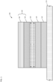
- Figure 1 illustrates a cross-sectional view of an electronic device.
- the electronic device comprises a semiconductor substrate 170 and an aluminum pad 110 placed thereon.
- the aluminum pad has an area (in plan view) of 1000 x 1000 square micrometers ( ⁇ m 2 ).
- Aluminum pads of any area could be used, for example having an area of 420 x 560 ⁇ m 2 or an area of 2040 x 1900 ⁇ m 2 .
- the electronic device further comprises a stack 100 which comprises a barrier layer 120 directly deposited on the aluminum pad 110, a seed layer 130 directly deposited on the barrier layer 120, and a metal layer 140 directly deposited on the seed layer 130.
- Exemplarily the stack 100 continuously and entirely covers the aluminum pad (in other words, the area - in plan view - of the stack is at least equal to the area - in plan view - of the aluminum pad).
- the metal layer 140 comprises a nickel sub-layer 150 and a palladium sub-layer of 160.
- the seed layer 130 may comprise a layer of copper.
- the seed layer 130 may comprise a single layer of copper, for example having a thickness less than 800 nanometers (nm), in particular having a thickness of 250-600 nm, and more in particular a thickness of about 300-500 nm.
- the barrier layer 120 may comprise titanium, titanium-nitride, titanium-tungsten, tantalum, and/or tantalum-nitride.
- the nickel sub-layer 150 of the metal layer 140 is directly deposited on the seed layer 130 and the palladium sub-layer 160 of the metal layer 140 is directly deposited on the nickel sub-layer 150 of the metal layer 140.
- the metal layer 140 may have a thickness greater than (or equal to) 500 nm.
- the nickel sub-layer 150 is at least 500 nm
- the palladium sub-layer 160 is at least 150 nm.
- the metal layer 140 may be deposited via electroless deposition (also termed e-less deposition), that is both the nickel and the palladium sub-layers 150, 160 may be deposited via electroless deposition.
- electroless deposition also termed e-less deposition
- Using electroless deposition enables the thickness of the nickel and palladium sub-layers 150, 160 to be modulated within a large range and with a greater thickness than with other deposition techniques.
- the thickness of the nickel and palladium sub-layers 150, 160 is modulated as a function of the technological purpose.
- the thickness can vary in a range of 500-5000 nm, depending on the technological purpose (e.g., barrier function, mechanical buffer function, and/or chemical reaction function).
- the nickel sub-layer may have a thickness able to withstand the nickel consumption (so that a certain thickness still remains in the final device) due to the wire bonding process (occurring in a later production phase) when the solder paste is positioned on the palladium.
- the palladium sub-layer 160 has the function to protect the nickel sub-layer 150 and to be wettable, therefore in some embodiments a range of 150-500 nm is used.
- the nickel sub-layer 150 Using electroless deposition enables the nickel sub-layer 150 to have for example a thickness in the abovesaid range of 500 nm to 5 micrometers.
- nickel-palladium metal layer 140 deposited by electroless deposition enables a greater total stack height as compared to other approaches that have been used, which may be desirable in some applications.
- the barrier layer 120 and the seed layer 130 may be deposited via physical vapor deposition. Alternatively, any suitable deposition method may be used for these layers.
- the width of the seed layer may be substantially constant from the barrier layer 120 to the metal layer 140.
- the expression "substantially constant” means that an actual width value of the seed layer varies, along a direction going from the barrier layer to the metal layer, within a range of +/- 10% (and preferably of +/- 5 %) from a nominal width value.
- the nominal width value may be 1000 ⁇ m and the actual width value may be between 900 ⁇ m and 1100 ⁇ m.
- dashed lines 180, 190 indicating the width of the seed layer 130
- dashed line 180 indicating the width at a lower point of the seed layer 130 (i.e., closer to the barrier layer 120)
- dashed line 190 indicating the width at a higher point of the seed layer 130 (i.e., closer to the nickel sub-layer 150).
- Figure 2 illustrates a cross-sectional view of a stack of an electronic device, in accordance with an embodiment of the present disclosure.
- the electronic device comprises a semiconductor substrate 270 and an aluminum pad 210 placed thereon.
- the electronic device further comprises a stack 200 which comprises a barrier layer 220 directly deposited on the aluminum pad 210, a seed layer 230 (such as copper) directly deposited on the barrier layer 220, and a metal layer 240 directly deposited on the seed layer 230.
- a stack 200 which comprises a barrier layer 220 directly deposited on the aluminum pad 210, a seed layer 230 (such as copper) directly deposited on the barrier layer 220, and a metal layer 240 directly deposited on the seed layer 230.
- the metal layer 240 comprises a nickel sub-layer 250 and a palladium sub-layer 260.
- the nickel sub-layer 250 of the metal layer 240 substantially covers a top surface 280 of the seed layer 230.
- the electroless deposition of the nickel sub-layer 250 causes a partial deposition of the nickel also on at least a portion of the sidewall 290 of the seed layer 230, thus completely covering the top surface 280 of the seed layer 230.
- the stacks 100, 200 of figures 1 , 2 may be manufactured by:
- the stack as described herein provides a more uniform interface among the different layers and thereby avoids delayering, as compared to other approaches that have been used. Moreover, the presence of the barrier and seed layers between the aluminum pad and the nickel sub-layer allows to avoid the direct deposition of the nickel, for example through the e-less process, on the aluminum. In fact, Applicant has verified that the e-less chemistry for depositing the nickel on aluminum could cause a damaging of the pad that is difficult to predict.
- the interposition of barrier layer 120, 220 and seed layer 130, 230 allows to obtain a more regular surface of the aluminum pad on one side, and, on the other, the deposition of the nickel on a surface (i.e., the seed layer) substantially insensitive to the action of the e-less chemistry, thus achieving an overall better interface.
- the disclosed structure may be used with any electronic device having an aluminum pad requiring a wettable/brasable metal, including but not limited to SiC devices as described herein, as well as gallium nitride or silicon devices (e.g., insulated-gate bipolar transistors (IGBT)).
- SiC devices as described herein, as well as gallium nitride or silicon devices (e.g., insulated-gate bipolar transistors (IGBT)).
- IGBT insulated-gate bipolar transistors
- the device may be any electronic device which has one or more aluminum pads, such as but not limited to silicon and/or silicon carbide (SiC) power devices.
- Non-limiting examples of power devices are metal-oxide-semiconductor field-effect transistors (MOSFETs), insulated-gate bipolar transistors (IGBT), and Schottky barrier diodes.
Landscapes
- Internal Circuitry In Semiconductor Integrated Circuit Devices (AREA)
- Electrodes Of Semiconductors (AREA)
Abstract
Electronic device comprising a semiconductor substrate (170), an aluminum pad (110) on the semiconductor substrate, and a stack (100). The stack (100) comprises, in sequence, a barrier layer (120) directly deposited on the aluminum pad, a seed layer (130) directly deposited on the barrier layer, the seed layer comprising copper and having a thickness less than 800 nanometers, and a metal layer (140) directly deposited on the seed layer, the metal layer comprising nickel and palladium.
Description
- The present invention relates generally to integrated circuit fabrications and, more particularly, to brasable metal layers on aluminum pads of integrated circuits.
- In the field of power devices (e.g., silicon carbide (SiC) technology), there is need to cover the aluminum pad of such devices with a brasable (or wettable) metal. A brasable metal is a metal able to be uniformly covered by a solder paste. This allows a stable attachment of the clips used in packaging to the aluminum pad.
- Currently, the coverage of brazable metal on aluminum metallizations (e.g., 450 nm thick) can be achieved by a PVD (Physical Vapor Deposition) of a Ti/NiV/Ag (titanium/nickel vanadium/silver) layer, with thicknesses of 150/300/500 nm, respectively or an e-less (Electroless) deposition of a Ni/Pd/Au (nickel/palladium/gold) layer.
- However, current solutions of brazable metal deposition on aluminum pads may have the disadvantages of creating insufficiently strong contacts and not being fully adaptable to the needs of the electronic device end-user during the soldering steps, for example, due to delamination of the NiV/Ag interface and due to limited NiV thicknesses; in addition, the e-less deposition technique may cause, especially for relatively large pads, inherent corrosion problems of the Ni layers due to the Au immersion reaction.
- Therefore, the problem arises of developing an electronic device with brazable metal pad coverage and related method that overcomes the disadvantages of the prior art.
- According to the invention, an electronic device and a method for manufacturing an electronic device are provided, as defined in the attached claims.
- Reference will now be made to the accompanying drawings, which are not necessarily drawn to scale, and wherein:
-
Fig 1 is a cross-sectional view of an example portion of an electronic device, in accordance with an embodiment of the present disclosure; and -
Fig. 2 is a cross-sectional view of an example portion of an electronic device, in accordance with an alternative embodiment of the present disclosure. - As used herein, terms such as "front," "rear," "top," etc. are used for explanatory purposes in the examples provided below to describe the relative position of certain components or portions of components. Furthermore, as would be evident to one of ordinary skill in the art in light of the present disclosure, the terms "substantially" and "approximately" indicate that the referenced element or associated description is accurate to within applicable engineering tolerances.
- The present disclosure overcomes the above technical challenges and difficulties based on providing nickel-palladium (Ni-Pd) as a brasable metal layer on an aluminum pad of an electronic device, which provides good coverage by the solder paste for attaching a clip to the aluminum pad.
-
Figure 1 illustrates a cross-sectional view of an electronic device. As seen infigure 1 , the electronic device comprises asemiconductor substrate 170 and analuminum pad 110 placed thereon. For example, the aluminum pad has an area (in plan view) of 1000 x 1000 square micrometers (µm2). Aluminum pads of any area could be used, for example having an area of 420 x 560 µm2 or an area of 2040 x 1900 µm2. - The electronic device further comprises a
stack 100 which comprises abarrier layer 120 directly deposited on thealuminum pad 110, aseed layer 130 directly deposited on thebarrier layer 120, and ametal layer 140 directly deposited on theseed layer 130. - Exemplarily the
stack 100 continuously and entirely covers the aluminum pad (in other words, the area - in plan view - of the stack is at least equal to the area - in plan view - of the aluminum pad). - In
figure 1 , themetal layer 140 comprises anickel sub-layer 150 and a palladium sub-layer of 160. - The
seed layer 130 may comprise a layer of copper. Theseed layer 130 may comprise a single layer of copper, for example having a thickness less than 800 nanometers (nm), in particular having a thickness of 250-600 nm, and more in particular a thickness of about 300-500 nm. - The
barrier layer 120 may comprise titanium, titanium-nitride, titanium-tungsten, tantalum, and/or tantalum-nitride. - For example, the
nickel sub-layer 150 of themetal layer 140 is directly deposited on theseed layer 130 and thepalladium sub-layer 160 of themetal layer 140 is directly deposited on thenickel sub-layer 150 of themetal layer 140. - The
metal layer 140 may have a thickness greater than (or equal to) 500 nm. In particular, thenickel sub-layer 150 is at least 500 nm, and thepalladium sub-layer 160 is at least 150 nm. - The
metal layer 140 may be deposited via electroless deposition (also termed e-less deposition), that is both the nickel and thepalladium sub-layers - Using electroless deposition enables the thickness of the nickel and
palladium sub-layers - The thickness of the nickel and
palladium sub-layers nickel sub-layer 150, the thickness can vary in a range of 500-5000 nm, depending on the technological purpose (e.g., barrier function, mechanical buffer function, and/or chemical reaction function). For example, the nickel sub-layer may have a thickness able to withstand the nickel consumption (so that a certain thickness still remains in the final device) due to the wire bonding process (occurring in a later production phase) when the solder paste is positioned on the palladium. - The
palladium sub-layer 160 has the function to protect thenickel sub-layer 150 and to be wettable, therefore in some embodiments a range of 150-500 nm is used. - Using electroless deposition enables the
nickel sub-layer 150 to have for example a thickness in the abovesaid range of 500 nm to 5 micrometers. - The use of a nickel-
palladium metal layer 140 deposited by electroless deposition enables a greater total stack height as compared to other approaches that have been used, which may be desirable in some applications. - The
barrier layer 120 and theseed layer 130 may be deposited via physical vapor deposition. Alternatively, any suitable deposition method may be used for these layers. - The width of the seed layer may be substantially constant from the
barrier layer 120 to themetal layer 140. For the purposes of the present disclosure, the expression "substantially constant" means that an actual width value of the seed layer varies, along a direction going from the barrier layer to the metal layer, within a range of +/- 10% (and preferably of +/- 5 %) from a nominal width value. For example, the nominal width value may be 1000 µm and the actual width value may be between 900 µm and 1100 µm. This is illustrated infigure 1 by the substantially equal length dashed lines 180, 190 indicating the width of theseed layer 130, with the dashed line 180 indicating the width at a lower point of the seed layer 130 (i.e., closer to the barrier layer 120) and the dashed line 190 indicating the width at a higher point of the seed layer 130 (i.e., closer to the nickel sub-layer 150). -
Figure 2 illustrates a cross-sectional view of a stack of an electronic device, in accordance with an embodiment of the present disclosure. - As seen in
figure 2 , the electronic device comprises asemiconductor substrate 270 and analuminum pad 210 placed thereon. - The electronic device further comprises a
stack 200 which comprises abarrier layer 220 directly deposited on thealuminum pad 210, a seed layer 230 (such as copper) directly deposited on thebarrier layer 220, and ametal layer 240 directly deposited on theseed layer 230. - In
figure 2 , themetal layer 240 comprises anickel sub-layer 250 and apalladium sub-layer 260. - In
figure 2 , thenickel sub-layer 250 of themetal layer 240 substantially covers atop surface 280 of theseed layer 230. Here, as illustrated, the electroless deposition of thenickel sub-layer 250 causes a partial deposition of the nickel also on at least a portion of thesidewall 290 of theseed layer 230, thus completely covering thetop surface 280 of theseed layer 230. - The
stacks figures 1 ,2 may be manufactured by: - providing an
aluminum pad semiconductor substrate - forming the stack on the aluminum pad, by:
- depositing a
barrier layer aluminum pad - depositing a
seed layer barrier layer metal layer seed layer
- depositing a
- The stack as described herein provides a more uniform interface among the different layers and thereby avoids delayering, as compared to other approaches that have been used. Moreover, the presence of the barrier and seed layers between the aluminum pad and the nickel sub-layer allows to avoid the direct deposition of the nickel, for example through the e-less process, on the aluminum. In fact, Applicant has verified that the e-less chemistry for depositing the nickel on aluminum could cause a damaging of the pad that is difficult to predict.
- In embodiments of the present disclosure, the interposition of
barrier layer seed layer - The disclosed structure may be used with any electronic device having an aluminum pad requiring a wettable/brasable metal, including but not limited to SiC devices as described herein, as well as gallium nitride or silicon devices (e.g., insulated-gate bipolar transistors (IGBT)).
- Finally, it is clear that modifications and variations may be made to what has been described and illustrated herein, without thereby departing from the scope of this disclosure, as defined in the annexed claims. For example, the device may be any electronic device which has one or more aluminum pads, such as but not limited to silicon and/or silicon carbide (SiC) power devices. Non-limiting examples of power devices are metal-oxide-semiconductor field-effect transistors (MOSFETs), insulated-gate bipolar transistors (IGBT), and Schottky barrier diodes.
- Examples of the present disclosure are the following:
- Example 1. An electronic device comprising:
- a semiconductor substrate;
- an aluminum pad on the semiconductor substrate; and
- a stack comprising, in sequence:
- a barrier layer directly deposited on the aluminum pad;
- a seed layer directly deposited on the barrier layer, the seed layer comprising copper and having a thickness less than 800 nanometers (nm); and
- a metal layer directly deposited on the seed layer, the metal layer comprising nickel and palladium.
- Example 2. The electronic device of example 1, wherein the metal layer comprises a first metal sub-layer comprising nickel directly deposited on the seed layer and a second metal sub-layer comprising palladium directly deposited on the first metal sub-layer.
- Example 3. The electronic device of example 2, wherein the first metal sub-layer entirely covers a top surface of the seed layer.
- Example 4. The electronic device of example 2, wherein the metal layer consists of the first and second metal sub-layers.
- Example 5. The electronic device of example 1, wherein the seed layer has a thickness of 250-600 nm.
- Example 6. The electronic device of example 1, wherein the metal layer has a thickness greater than 500 nm.
- Example 7. The electronic device of example 1, wherein a sectional view of the seed layer has a substantially constant width from the barrier layer to the metal layer.
- Example 8. The electronic device of example 1, wherein the seed layer consists of a single layer of copper.
- Example 9. The electronic device of example 1, wherein the barrier layer comprises titanium, titanium-nitride, titanium-tungsten, tantalum, and/or tantalum-nitride.
- Example 10. The electronic device of example 1, wherein the barrier layer consists of a layer made of titanium, titanium-nitride, titanium-tungsten, tantalum, and/or tantalum-nitride.
- Example 11. A method of manufacturing an electronic device, the method comprising:
- providing an aluminum pad on a semiconductor substrate of the electronic device; and
- forming a stack on the aluminum pad, the forming comprising:
- depositing a barrier layer directly on the aluminum pad;
- depositing a seed layer directly on the barrier layer, the seed layer comprising copper and having a thickness less than 800 nanometers (nm); and
- depositing a metal layer directly on the seed layer, the metal layer comprising nickel and palladium.
- Example 12. The method of example 11, wherein depositing the metal layer is performed via electroless deposition.
- Example 13. The method of example 11, wherein depositing the barrier layer and the seed layer are performed via physical vapor deposition.
- Example 14. The method of example 11, wherein depositing the metal layer directly on the seed layer comprises depositing a first metal sub-layer comprising nickel directly on the seed layer and depositing a second metal sub-layer comprising palladium directly on the first metal sub-layer.
- Example 15. The method of example 14, wherein the first metal sub-layer substantially entirely covers a top surface of the seed layer.
- Example 16. The method of example 11, wherein the seed layer is deposited with a thickness of 250-600 nm.
- Example 17. The method of example 11, wherein the metal layer is deposited with a thickness greater than 500 nm.
- Example 18. The method of example 11, wherein a sectional view of the seed layer has a substantially constant width from the barrier layer to the metal layer.
- Example 19. The method of example 11, wherein the seed layer is deposited as a single layer of copper.
- Example 20. The method of example 11, wherein the barrier layer is deposited as a single layer of titanium, titanium-nitride, titanium-tungsten, tantalum, and/or tantalum-nitride.
Claims (15)
- An electronic device comprising:a semiconductor substrate (170; 270);an aluminum pad (110; 210) on the semiconductor substrate (170; 270); anda stack (100; 200) comprising, in sequence:a barrier layer (120; 220) directly deposited on the aluminum pad (110; 210);a seed layer (130; 230) directly deposited on the barrier layer (120; 220), the seed layer (130; 230) comprising copper and having a thickness less than 800 nanometers ; anda metal layer (140; 240) directly deposited on the seed layer (130; 230), the metal layer (140; 240) comprising nickel and palladium.
- The electronic device of claim 1, wherein the metal layer (140; 240) comprises a first metal sub-layer (150; 250) comprising nickel directly deposited on the seed layer (130; 230) and a second metal sub-layer (160; 260) comprising palladium directly deposited on the first metal sub-layer (150; 250).
- The electronic device of claim 2, wherein the first metal sub-layer (150; 250) entirely covers a top surface of the seed layer (130; 230).
- The electronic device of claim 2, wherein the metal layer (140; 240) consists of the first (150; 250) and second (160; 260) metal sub-layers.
- The electronic device of any of the preceding claims, wherein the seed layer (130; 230) has a thickness of 250-600 nm.
- The electronic device of any of the preceding claims, wherein the metal layer (140; 240) has a thickness greater than 500 nm.
- The electronic device of any of the preceding claims, wherein a sectional view of the seed layer (130; 230) has a substantially constant width from the barrier layer (120; 220) to the metal layer (140; 240).
- The electronic device of any of the preceding claims, wherein the seed layer (130; 230) consists of a single layer of copper.
- The electronic device of any of the preceding claim, wherein the barrier layer (120; 220) comprises titanium, titanium-nitride, titanium-tungsten, tantalum, and/or tantalum-nitride.
- The electronic device of claim 1, wherein the barrier layer (120; 220) consists of a layer made of titanium, titanium-nitride, titanium-tungsten, tantalum, and/or tantalum-nitride.
- A method of manufacturing an electronic device, the method comprising:providing an aluminum pad (110; 210) on a semiconductor substrate (170; 270 of the electronic device; andforming a stack (100; 200) on the aluminum pad, the forming comprising:depositing a barrier layer (120; 220) directly on the aluminum pad (110; 210);depositing a seed layer (130; 230) directly on the barrier layer (120; 220) , the seed layer comprising copper and having a thickness less than 800 nanometers; anddepositing a metal layer (140; 240) directly on the seed layer (130; 230), the metal layer comprising nickel and palladium.
- The method of claim 11, wherein depositing the metal layer (140; 240) is performed via electroless deposition.
- The method of claim 11 or 12, wherein depositing the barrier layer (120; 220) and the seed layer (130; 230) are performed via physical vapor deposition.
- The method of any of claims 11-13, wherein depositing the metal layer (140; 240) comprises depositing a first metal sub-layer (150; 250) comprising nickel directly on the seed layer (130; 230) and depositing a second metal sub-layer (160; 260) comprising palladium directly on the first metal sub-layer, wherein the first metal sub-layer substantially entirely covers a top surface of the seed layer.
- The method of claim 11, wherein the seed layer (130; 230) is deposited as a single layer of copper.
Applications Claiming Priority (1)
| Application Number | Priority Date | Filing Date | Title |
|---|---|---|---|
| US18/526,447 US20250183174A1 (en) | 2023-12-01 | 2023-12-01 | Electronic device having a brasable metal pad cover and associated method |
Publications (1)
| Publication Number | Publication Date |
|---|---|
| EP4571830A1 true EP4571830A1 (en) | 2025-06-18 |
Family
ID=93562461
Family Applications (1)
| Application Number | Title | Priority Date | Filing Date |
|---|---|---|---|
| EP24212918.7A Pending EP4571830A1 (en) | 2023-12-01 | 2024-11-14 | Electronic device having a brasable metal pad cover and associated method |
Country Status (3)
| Country | Link |
|---|---|
| US (1) | US20250183174A1 (en) |
| EP (1) | EP4571830A1 (en) |
| CN (1) | CN120089648A (en) |
Citations (4)
| Publication number | Priority date | Publication date | Assignee | Title |
|---|---|---|---|---|
| US20070023919A1 (en) * | 2005-07-29 | 2007-02-01 | Mou-Shiung Lin | Bonding pad on ic substrate and method for making the same |
| US20110215446A1 (en) * | 2006-09-06 | 2011-09-08 | Megica Corporation | Chip package and method for fabricating the same |
| US20120064712A1 (en) * | 2010-09-14 | 2012-03-15 | Taiwan Semiconductor Manufacturing Company, Ltd. | Method for Reducing UBM Undercut in Metal Bump Structures |
| US20200395332A1 (en) * | 2019-06-12 | 2020-12-17 | Nxp Usa, Inc. | Package with conductive underfill ground plane |
Family Cites Families (2)
| Publication number | Priority date | Publication date | Assignee | Title |
|---|---|---|---|---|
| US7217656B2 (en) * | 2005-05-31 | 2007-05-15 | Texas Instruments Incorporated | Structure and method for bond pads of copper-metallized integrated circuits |
| US8232193B2 (en) * | 2010-07-08 | 2012-07-31 | Taiwan Semiconductor Manufacturing Company, Ltd. | Method of forming Cu pillar capped by barrier layer |
-
2023
- 2023-12-01 US US18/526,447 patent/US20250183174A1/en active Pending
-
2024
- 2024-11-14 EP EP24212918.7A patent/EP4571830A1/en active Pending
- 2024-11-27 CN CN202411708142.3A patent/CN120089648A/en active Pending
Patent Citations (4)
| Publication number | Priority date | Publication date | Assignee | Title |
|---|---|---|---|---|
| US20070023919A1 (en) * | 2005-07-29 | 2007-02-01 | Mou-Shiung Lin | Bonding pad on ic substrate and method for making the same |
| US20110215446A1 (en) * | 2006-09-06 | 2011-09-08 | Megica Corporation | Chip package and method for fabricating the same |
| US20120064712A1 (en) * | 2010-09-14 | 2012-03-15 | Taiwan Semiconductor Manufacturing Company, Ltd. | Method for Reducing UBM Undercut in Metal Bump Structures |
| US20200395332A1 (en) * | 2019-06-12 | 2020-12-17 | Nxp Usa, Inc. | Package with conductive underfill ground plane |
Also Published As
| Publication number | Publication date |
|---|---|
| CN120089648A (en) | 2025-06-03 |
| US20250183174A1 (en) | 2025-06-05 |
Similar Documents
| Publication | Publication Date | Title |
|---|---|---|
| US6346469B1 (en) | Semiconductor device and a process for forming the semiconductor device | |
| EP1412989B1 (en) | Light emitting diodes including modifications for submount bonding | |
| TWI243488B (en) | Electrical contact-area for optoelectronic semiconductor-chip and its production method | |
| US8283758B2 (en) | Microelectronic packages with enhanced heat dissipation and methods of manufacturing | |
| US11842975B2 (en) | Electronic device with multi-layer contact and system | |
| US10573611B2 (en) | Solder metallization stack and methods of formation thereof | |
| US20040070042A1 (en) | Method of wire bonding over active area of a semiconductor circuit | |
| US6564449B1 (en) | Method of making wire connection in semiconductor device | |
| TWI629808B (en) | Light-emitting diode having a stress buffer layer under the metallization layer | |
| US20120146204A1 (en) | Semiconductor devices and electrical parts manufacturing using metal coated wires | |
| KR20040111395A (en) | Wafer-level coated copper stud bumps | |
| JP2001351940A (en) | Copper interconnect wiring in IC chip | |
| US7709938B2 (en) | Arrangement for electrically connecting semiconductor circuit arrangements to an external contact device and method for producing the same | |
| US20110006409A1 (en) | Nickel-titanum contact layers in semiconductor devices | |
| WO2007146478A1 (en) | Microelectronic assembly with back side metallization and method for forming the same | |
| CN206639796U (en) | Semiconductor devices | |
| US20110031596A1 (en) | Nickel-titanum soldering layers in semiconductor devices | |
| US20110027984A1 (en) | Process of forming an electronic device including a conductive stud over a bonding pad region | |
| US20090051016A1 (en) | Electronic component with buffer layer | |
| US8368211B2 (en) | Solderable top metalization and passivation for source mounted package | |
| US8722528B2 (en) | Die backside standoff structures for semiconductor devices | |
| CN112885803A (en) | Semiconductor structure and manufacturing method thereof | |
| US20070231954A1 (en) | Gold/silicon eutectic die bonding method | |
| US20070080391A1 (en) | Semiconductor device with front side metallization and method for the production thereof | |
| US20250183174A1 (en) | Electronic device having a brasable metal pad cover and associated method |
Legal Events
| Date | Code | Title | Description |
|---|---|---|---|
| PUAI | Public reference made under article 153(3) epc to a published international application that has entered the european phase |
Free format text: ORIGINAL CODE: 0009012 |
|
| STAA | Information on the status of an ep patent application or granted ep patent |
Free format text: STATUS: THE APPLICATION HAS BEEN PUBLISHED |
|
| AK | Designated contracting states |
Kind code of ref document: A1 Designated state(s): AL AT BE BG CH CY CZ DE DK EE ES FI FR GB GR HR HU IE IS IT LI LT LU LV MC ME MK MT NL NO PL PT RO RS SE SI SK SM TR |
|
| STAA | Information on the status of an ep patent application or granted ep patent |
Free format text: STATUS: THE APPLICATION IS DEEMED TO BE WITHDRAWN |