EP4568267A1 - Leakage correction device and image sensor - Google Patents
Leakage correction device and image sensor Download PDFInfo
- Publication number
- EP4568267A1 EP4568267A1 EP24217945.5A EP24217945A EP4568267A1 EP 4568267 A1 EP4568267 A1 EP 4568267A1 EP 24217945 A EP24217945 A EP 24217945A EP 4568267 A1 EP4568267 A1 EP 4568267A1
- Authority
- EP
- European Patent Office
- Prior art keywords
- pixel
- leakage
- circuit
- output
- compensation device
- Prior art date
- Legal status (The legal status is an assumption and is not a legal conclusion. Google has not performed a legal analysis and makes no representation as to the accuracy of the status listed.)
- Pending
Links
Images



Classifications
-
- H—ELECTRICITY
- H04—ELECTRIC COMMUNICATION TECHNIQUE
- H04N—PICTORIAL COMMUNICATION, e.g. TELEVISION
- H04N25/00—Circuitry of solid-state image sensors [SSIS]; Control thereof
- H04N25/60—Noise processing, e.g. detecting, correcting, reducing or removing noise
- H04N25/67—Noise processing, e.g. detecting, correcting, reducing or removing noise applied to fixed-pattern noise, e.g. non-uniformity of response
- H04N25/671—Noise processing, e.g. detecting, correcting, reducing or removing noise applied to fixed-pattern noise, e.g. non-uniformity of response for non-uniformity detection or correction
- H04N25/673—Noise processing, e.g. detecting, correcting, reducing or removing noise applied to fixed-pattern noise, e.g. non-uniformity of response for non-uniformity detection or correction by using reference sources
-
- H—ELECTRICITY
- H04—ELECTRIC COMMUNICATION TECHNIQUE
- H04N—PICTORIAL COMMUNICATION, e.g. TELEVISION
- H04N17/00—Diagnosis, testing or measuring for television systems or their details
- H04N17/002—Diagnosis, testing or measuring for television systems or their details for television cameras
-
- H—ELECTRICITY
- H04—ELECTRIC COMMUNICATION TECHNIQUE
- H04N—PICTORIAL COMMUNICATION, e.g. TELEVISION
- H04N25/00—Circuitry of solid-state image sensors [SSIS]; Control thereof
- H04N25/70—SSIS architectures; Circuits associated therewith
- H04N25/702—SSIS architectures characterised by non-identical, non-equidistant or non-planar pixel layout
-
- H—ELECTRICITY
- H04—ELECTRIC COMMUNICATION TECHNIQUE
- H04N—PICTORIAL COMMUNICATION, e.g. TELEVISION
- H04N25/00—Circuitry of solid-state image sensors [SSIS]; Control thereof
- H04N25/70—SSIS architectures; Circuits associated therewith
- H04N25/76—Addressed sensors, e.g. MOS or CMOS sensors
- H04N25/766—Addressed sensors, e.g. MOS or CMOS sensors comprising control or output lines used for a plurality of functions, e.g. for pixel output, driving, reset or power
-
- H—ELECTRICITY
- H04—ELECTRIC COMMUNICATION TECHNIQUE
- H04N—PICTORIAL COMMUNICATION, e.g. TELEVISION
- H04N25/00—Circuitry of solid-state image sensors [SSIS]; Control thereof
- H04N25/70—SSIS architectures; Circuits associated therewith
- H04N25/76—Addressed sensors, e.g. MOS or CMOS sensors
- H04N25/77—Pixel circuitry, e.g. memories, A/D converters, pixel amplifiers, shared circuits or shared components
-
- H—ELECTRICITY
- H04—ELECTRIC COMMUNICATION TECHNIQUE
- H04N—PICTORIAL COMMUNICATION, e.g. TELEVISION
- H04N25/00—Circuitry of solid-state image sensors [SSIS]; Control thereof
- H04N25/70—SSIS architectures; Circuits associated therewith
- H04N25/76—Addressed sensors, e.g. MOS or CMOS sensors
- H04N25/77—Pixel circuitry, e.g. memories, A/D converters, pixel amplifiers, shared circuits or shared components
- H04N25/771—Pixel circuitry, e.g. memories, A/D converters, pixel amplifiers, shared circuits or shared components comprising storage means other than floating diffusion
-
- H—ELECTRICITY
- H04—ELECTRIC COMMUNICATION TECHNIQUE
- H04N—PICTORIAL COMMUNICATION, e.g. TELEVISION
- H04N25/00—Circuitry of solid-state image sensors [SSIS]; Control thereof
- H04N25/50—Control of the SSIS exposure
- H04N25/53—Control of the integration time
- H04N25/532—Control of the integration time by controlling global shutters in CMOS SSIS
Definitions
- the embodiment relates to a leakage correction device and an image sensor.
- An image sensor recognizes (or detects) a location or movement based on a distance from an object, and is widely used in all industrial fields.
- An image sensor sequentially outputs electric signals for each row and line. In this case, there is a problem that the leakage amount increases as the output signal is output later, and the detection performance for an object deteriorates.
- An object of the embodiment is to solve the above-mentioned problems and other problems.
- Another object of the embodiment is to provide a leakage correction device and an image sensor that can improve the detection performance for an object.
- the leakage compensation device may include a pixel array including a plurality of row lines each including a plurality of pixel circuits, configured to store electric signals corresponding to light in the plurality of pixel circuits during a capture section, and sequentially output the stored electric signals by row line whenever a preset time elapses for each row line during an output section; and a plurality of detection circuits configured to detect leakage signals for compensating the outputted electric signals.
- the pixel circuit may include a photodetector configured to detect the light; and an output circuit configured to store and output the electric signal corresponding to the detected light.
- the detection circuit may have the same circuit structure as the circuit structure of the output circuit.
- Each of the outputted electric signals may be a value reduced by the value leaked during the preset time from each of the stored electric signals.
- the leakage signal may be the same as the leaked value.
- the electric signal and the leakage signal may be output simultaneously or differently.
- the detection circuit may be positioned within the pixel circuit.
- the detection circuit may be positioned corresponding to the pixel circuit.
- the leakage compensation device may further include a readout line commonly connected to the pixel circuit and the detection circuit.
- the detection circuit may be arranged adjacent to the at least two or more pixel circuits to detect a leakage signal of each of the at least two or more pixel circuits.
- the leakage compensation device may further include a first readout line commonly connected to the at least two pixel circuits; and a second readout line connected to the detection circuit.
- the leakage compensation device may include at least one dummy pixel area around the pixel array; and the detection circuit may be provided at at least one position of the at least one dummy pixel area.
- an image sensor may include a pixel array including a plurality of row lines each including a plurality of pixel circuits, configured to store electric signals corresponding to light in the plurality of pixel circuits during a capture section, and sequentially output the stored electric signals by row line whenever a preset time elapses for each row line during an output section; and a plurality of detection circuits configured to detect leakage signals from the electric signals of the pixel circuit.
- the image sensor may further include a correction circuit configured to correct the outputted electric signals using the leakage signals.
- An output timing of the electric signal of the pixel circuit and the leakage signal of the detection circuit may be different each other.
- the image sensor may further include a correction circuit configured to correct the electric signals outputted from the pixel circuits based on the leakage signals that are leaked differently at different preset times.
- the image sensor may further include a readout line that is commonly connected to the pixel circuit and the detection circuit.
- the two or more pixel circuits may sequentially output electric signals through the first readout line using time division, respectively.
- the detection circuit may be configured to sequentially output a leakage signal through a second readout line as many as the number of pixel circuits by using using time division.
- the image sensor may include at least one dummy pixel area around the pixel array.
- the pixel circuit may correct the electric signals by using detection signals detected by the detection circuits located in the at least one dummy pixel area.
- the correction circuit may be configured to perform an operation of adding the leakage data to each sensing data, and obtain the original sensing data.
- the electric signals output from the pixel circuits are compensated based on the leakage signals that are leaked differently at different preset times, so that the detection performance for the object can be improved.
- the leakage signal that is the same as the value leaked from the electric signal of the pixel circuit in the detection circuit can be compensated based on the leakage signal. Accordingly, the original electric signal before leakage is obtained, so that the loss of image data is prevented, so that the detection performance for the object can be improved.
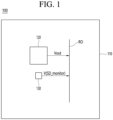
- FIG. 1 illustrates a leakage compensation device according to a first embodiment.
- the leakage compensation device 100 may include a pixel array 110, a detection circuit 130, etc.
- the pixel array 110 may include M pixel circuits 120.
- the M pixel circuits 120 may be arranged in a matrix form, for example, but are not limited thereto.
- the pixel array 110 may include a plurality of row lines (L1 to L12). Each of the row lines (L1 to L12) may include N (N ⁇ M) or more pixel circuits.
- the leakage compensation device 100 may be operated as an image sensor of a global shutter method.
- the image sensor of the global shutter method may include a reset section (T11), a capture section (T12), an output section (T13), etc.
- the reset section (T11) may be called an initialization section
- the capture section (T12) may be called a storage section
- the output section (T13) may be called a readout section.
- M pixel circuits 120 may be reset.
- the leakage signal (V(SD_monitor)) can be a current, a voltage, a potential, etc. formed by leaked charges, for example, electrons.
- the detection circuit 130 can be provided in the pixel array 110.
- the detection circuit 130 can be positioned corresponding to each of the plurality of pixel circuits 120. For example, if the pixel array 110 is equipped with one million pixel circuits 120, one million detection circuits 130 may also be equipped in the pixel array 110 corresponding to each of the one million pixel circuits 120.
- the output electric signals (Vout) are compensated for with the original electric signals using the leakage signals, so that the detection performance for the object can be improved.
- the pixel circuit 120 and the detection circuit 130 may be commonly connected to the readout line (RO).
- the electric signal (Vout) of the pixel circuit 120 may be output through the readout line (RO) using time division, and then the leakage signal of the detection circuit 130 may be output through the readout line (RO).
- the opposite operation may also be performed.
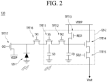
- the pixel circuit 120 may include a photodetector 120-1, an output circuit 120-2, etc.
- the photodetector 120-1 may detect light and obtain an electric signal corresponding to the light.
- the photodetector 120-1 may be configured as a semiconductor light emitting diode.
- transistors 120-2 in FIG. 2 Although five transistors are shown in the output circuit 120-2 in FIG. 2 , fewer or more transistors may be provided.
- the output circuit 120-2 may include a first transistor (TFT11), a second transistor (TFT12), a third transistor (TFT13), a fourth transistor (TFT14), and a fifth transistor (TFT15).
- TFT11 may be called a storage transistor
- the second transistor (TFT12) may be called a transmission transistor
- the third transistor (TFT13) may be called a reset transistor.
- the fourth transistor (TFT14) may be called a driving transistor
- the fifth transistor (TFT15) may be called a selection transistor.
- the first transistor (TFT11) may be connected to a photodetector 120-1 and may store an electric signal obtained from the photodetector 120-1 in the storage capacitor (SD).
- the second transistor (TFT12) may be connected to the first transistor (TFT11) and may transmit and store an electric signal stored in the storage capacitor (SD) to the floating diffusion (FD).
- the third transistor (TFT13) may reset a node between the second transistor (TFT12) and the fourth transistor (TFT14).
- the fourth transistor (TFT14) can output an electric signal stored in a floating diffusion (FD).
- the fourth transistor (TFT14) can operate as a source-follower amplifier, but is not limited thereto.
- the fifth transistor (TFT15) is connected between the fourth transistor (TFT14) and the readout line (RO), and can output an electric signal (Vout) passing through the driving transistor to the readout line (RO).
- the pixel circuit 120 may further include a sixth transistor, a seventh transistor, etc.
- the sixth transistor is connected between the photodetector 120-1 and the first transistor (TFT11), and can transmit and store an electric signal obtained from the photodetector 120-1 to a storage capacitor (SD).
- the sixth transistor may be called a transmission transistor.
- the seventh transistor may be commonly connected to the M pixel circuits 120 of the pixel array 110 and may reset the M pixel circuits 120.
- the seventh transistor may be provided in each of the M pixel circuits 120.
- the seventh transistor may be provided outside the M pixel circuits 120 and may be commonly connected to the M pixel circuits 120.
- the detection circuit 130 may have the same circuit structure as the circuit structure of the output circuit 120-2.
- the detection circuit 130 may detect a leakage signal (V(SD_monitor)). As described above, since the circuit structure of the detection circuit 130 is the same as that of the output circuit 120-2, the leakage signal (V(SD_monitor)) may be the same as the value leaked from the electric signal of the output circuit 120-2.
- transistors Although five transistors are illustrated in the detection circuit 130 in FIG. 3 , fewer or more transistors may be provided.
- the detection circuit 130 may include a first transistor (TFT21), a second transistor (TFT22), a third transistor (TFT23), a fourth transistor (TFT24), and a fifth transistor (TFT25).
- TFT21 may be called a monitoring transistor
- the second transistor (TFT22) may be called a transmission transistor
- the third transistor (TFT23) may be called a reset transistor.
- the fourth transistor (TFT24) may be called a driving transistor
- the fifth transistor (TFT25) may be called a selection transistor.
- the first transistor (TFT21) may monitor a leakage signal (V(SD_monitor)) for a preset section of time and store it in a storage capacitor (SD_monitor).
- V(SD_monitor) a leakage signal
- SD_monitor a storage capacitor
- the second transistor (TFT22) may be connected to the first transistor (TFT21) and may transmit and store the leakage signal (V(SD_monitor)) stored in the monitoring storage capacitor (SD_monitor) to a floating diffusion (FD).
- V(SD_monitor) the leakage signal stored in the monitoring storage capacitor (SD_monitor)
- the third transistor (TFT23) may reset a node between the second transistor (TFT22) and the fourth transistor (TFT24).
- the fifth transistor (TFT25) is connected between the fourth transistor (TFT24) and the readout line (RO), and can output a leakage signal (V(SD_monitor)) via the driving transistor to the readout line (RO).
- the first transistor (TFT21) is omitted, and the storage capacitor (SD_monitor) can be directly connected to the second transistor (TFT22).
- the leakage signal (V(SD_monitor)) stored in the storage capacitor (SD_monitor) can be transmitted to the floating diffusion (FD) via the second transistor (TFT22).
- the reset section (T11), the capture section (T12), and the output section (T13) can be defined as one cycle. This cycle can correspond to one frame or be a part of one frame.
- M pixel circuits 120 can be reset.
- the seventh transistor can be turned on by the overflow drain signal (OG), and M pixel circuits 120 of the pixel array 110 can be reset.
- OG overflow drain signal
- the third transistor (TFT13) of the pixel circuit 120 and the third transistor (TFT23) of the detection circuit 130 are turned on by the first reset signal (RES1) and the second reset signal (RES2), respectively, so that the node of the pixel circuit 120 and the node of the detection circuit 130 can be reset.
- the node of the pixel circuit 120 and the node of the detection circuit 130 may be reset at different times.
- the fifth transistor (TFT15) may be turned on by the first selection signal in the pixel circuit 120 and the node is reset through the readout line (RO)
- the fifth transistor (TFT25) may be turned on by the second selection circuit in the detection circuit 130 and the node may be reset through the readout line (RO).
- the sixth transistor and the first transistor (TFT11) may be turned on by the first transmission signal (TX1) and the storage gate signal (SG), respectively, so that an electric signal corresponding to light detected by the photodetector 120-1 may be stored in the storage capacitor (SD).
- the leakage signal (V(SD_monitor)) may be stored in the storage capacitor (SD_monitor) by the storage monitoring gate signal (SG_monitor).
- the second transistor (TFT12) is turned on by the second transmission signal (TX2), so that the electric signal stored in the storage capacitor (SD) may be transmitted and stored in the floating diffusion (FD).
- the second transistor (TFT22) is turned on by the transmission signal (TX2), so that the leakage signal (V(SD_monitor)) stored in the storage capacitor (SD_monitor) may be transmitted and stored in the floating diffusion (FD).
- the output timing of the electric signal (Vout) of the pixel circuit 120 and the leakage signal (V (SD_monitor)) of the detection circuit 130 can be different. That is, in the pixel circuit 120, the fifth transistor (TFT15) is turned on by the first selection signal, and the electric signal (Vout) stored in the floating diffusion (FD) is output through the readout line (RO), and then in the detection circuit 130, the fifth transistor (TFT25) is turned on by the second selection circuit, and the leakage signal (V(SD_monitor)) stored in the floating diffusion (FD) can be output through the readout line (RO).
- the electric signal (Vout) and the leakage signal (V(SD_monitor)) can be output (or obtained) at different times. That is, as illustrated in 5, the electric signal (Vout) stored in the pixel circuit 120 may be output first, and then the leakage signal (V(SD_monitor)) stored in the detection circuit 130 may be output.
- the time at which the electric signal is stored and then output in each pixel circuit 120 may be determined by a preset time.
- the first pixel circuit may be stored as an electric signal during the capture section (T12).
- an electric signal (Vout) output from a pixel circuit 120 can be compensated based on the leakage signal (V(SD_monitor)). Accordingly, an original electric signal before leakage is obtained, so that loss of image data is prevented, and detection performance for an object can be improved.
- FIG. 6 illustrates a leakage compensation device according to the second embodiment.
- the second embodiment is the same as the first embodiment except that the pixel circuit 120 and the detection circuit 130 are independently connected to the first readout line (RO1) and the second readout line (RO2), respectively.
- the same drawing reference numerals are given to components having the same structure or function as those of the first embodiment, and detailed descriptions are omitted.
- the leakage compensation device 100A may include a pixel array 110, a detection circuit 130, etc.
- the pixel array 110 may include M pixel circuits 120.
- a detection circuit 130 may be provided corresponding to each of the M pixel circuits 120. That is, the M detection circuits 130 may be provided.
- the pixel circuit 120 may be connected to the first readout line (RO1), and the detection circuit 130 may be connected to the second readout line (RO2).
- the electric signal (Vout) stored in the pixel circuit 120 and the leakage signal (V(SD_monitor)) stored in the detection circuit 130 may be individually output.
- the electric signal (Vout) and the leakage signal (V(SD_monitor)) may be output simultaneously or differently.
- the fifth transistor (TFT15) of the pixel circuit 120 and the fifth transistor (TFT25) of the detection circuit 130 are turned on at the same time by the first selection signal and the second selection signal, respectively, so that the electric signal (Vout) stored in the pixel circuit 120 and the leakage signal (V(SD_monitor)) stored in the detection circuit 130 can be simultaneously output through the first readout line (RO1) and the second readout line (RO2), respectively.
- FIG. 8 illustrates a leakage compensation device according to the third embodiment.
- the third embodiment is the same as the first embodiment and/or the second embodiment, except that the detection circuit 130 is located within the pixel circuit 120.
- the same drawing reference numerals are given to components having the same structure or function as those of the first embodiment and/or the second embodiment, and detailed descriptions are omitted.
- a leakage compensation device 100B may include a pixel array 110, a detection circuit 130, etc.
- the pixel array 110 may include M pixel circuits 120.
- a detection circuit 130 may be provided corresponding to each of the M pixel circuits 120. That is, M detection circuits 130 may be provided.
- the detection circuit 130 may be located within the pixel circuit 120.
- the detection circuit 130 may be physically located within the pixel circuit 120 or may be circuitically included within the pixel circuit 120.
- the detection circuit 130 illustrated in FIG. 3 may be included in the pixel circuit 120 illustrated in FIG. 2 .
- the detection circuit 130 may be located within the area where the pixel circuit 120 is formed.
- the pixel circuit 120 and the detection circuit 130 may be commonly connected to a line that shares a power supply (VDDP).
- VDDP power supply
- FIG. 9 illustrates a leakage compensation device according to the fourth embodiment.
- the fourth embodiment is similar to the first to third embodiments except that the detection circuit 130 is arranged adjacent to at least two or more pixel circuits 121 to 124.
- the same drawing reference numerals are given to components having the same structure or function as those of the first to third embodiments, and detailed descriptions are omitted.
- the leakage compensation device 100C may include a pixel array 110, a detection circuit 130, etc.
- the pixel array 110 may include M pixel circuits 120.
- the detection circuit 130 may be arranged adjacent to at least two pixel circuits 121 to 124.
- the detection circuit 130 may be surrounded by at least two pixel circuits 121 to 124, but is not limited thereto.
- the detection circuit 130 may be surrounded by four pixel circuits 121 to 124, but is not limited thereto.
- the detection circuit 130 may be located in a central region of an area composed of four pixel circuits 121 to 124.
- Four pixel circuits 121 to 124 may be connected to the first readout line (RO1), and the detection circuit 130 may be connected to the second readout line (RO2).
- the four pixel circuits 121 to 124 may sequentially output electric signals through the first readout line (RO1) using time division.
- the detection circuit 130 may sequentially output a leakage signal through the second readout line (RO2) as many times as the number of pixel circuits 121 to 124 using time division.
- RO2 second readout line
- the detection signal may output the first leakage signal when the electric signal of the first pixel circuit 121 is output.
- the first leakage signal may be the same as the value leaked from the electric signal of the first pixel circuit 121.
- the detection signal may output a second leakage signal when the electric signal of the second pixel circuit 122 is output.
- the second leakage signal may be the same as the value leaked from the electric signal of the second pixel circuit 122.
- the detection signal may output a third leakage signal when the electric signal of the third pixel circuit 123 is output.
- the third leakage signal may be the same as the value leaked from the electric signal of the third pixel circuit 123.
- the detection signal may output a fourth leakage signal when the electric signal of the fourth pixel circuit 124 is output.
- the fourth leakage signal may be the same as the value leaked from the electric signal of the fourth pixel circuit 124.
- four pixel circuits 121 to 124 and the detection circuit 130 may be commonly connected to the same readout line.
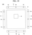
- FIG. 10 illustrates a leakage compensation device according to a fifth embodiment.
- the fifth embodiment is similar to the first to third embodiments except that the detection circuit 130 is located around the pixel array 110.
- the same reference numerals are given to components having the same structure or function as those of the first to fourth embodiments, and detailed descriptions are omitted.
- the leakage compensation device 100D may include a pixel array 110, a detection circuit 130, etc.
- the pixel array 110 may include M pixel circuits 120.
- the detection circuit 130 may be located around the pixel array 110.
- At least one dummy pixel region 151 to 154 may be positioned around the pixel array 110.
- the dummy pixel region 151 to 154 may include a plurality of pixel circuits, but the pixel circuits may not operate.
- four dummy pixel regions 151 to 154 may be positioned around the pixel array 110.
- the detection circuit 130 may be provided at at least one location of at least one dummy pixel region 151 to 154.
- two detection circuits 130 may be positioned in each of four dummy pixel regions (151 to 154).
- the electric signals of the N pixel circuits of the row line can be corrected using the detection signals detected by the detection circuits 130 (131a to 131c, 132a to 132c, 133a to 133c, 134a to 134c) positioned in each of four dummy pixel regions (151 to 154).
- the electric signals of the N pixel circuits of the row line may be corrected using the detection signals using an interpolation method.
- two detection circuits 130 may be positioned in each of the second dummy pixel area 152 and the fourth dummy pixel area 154, and no detection circuit 130 may be positioned in the first dummy pixel area 151 and the third dummy pixel area 153.
- two detection circuits 130 may be positioned in each of the first dummy pixel area 151 and the third dummy pixel area 153, and no detection circuit 130 may be positioned in the second dummy pixel area 152 and the fourth dummy pixel area 154.
- the detection circuits 130 may be located only in one of the first dummy pixel area 151 and the third dummy pixel area 153.
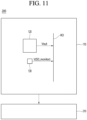
- FIG. 11 illustrates an image sensor according to an embodiment.
- the leakage compensation device according to the first embodiment FIGS. 1 to 5
- the leakage compensation device according to the second to fifth embodiments FIGS. 6 , 8 to 10
- FIGS. 6 , 8 to 10 may also be included in the image sensor according to the embodiment.
- the image sensor 200 may include a pixel array 110, a detection circuit 130, a correction circuit 210, etc.
- Each of the M pixel circuits 120 included in the pixel array 110 may include a photodetector 120-1 and an output circuit 120-2.
- the correction circuit 210 may correct the electric signals (Vout) output from the plurality of pixel circuits 120 using the leakage signals (V(SD_monitor)) output from the detection circuit 130.
- the detection circuit 130 may have the same circuit structure as the circuit structure of the output circuit 120-2. Accordingly, the leakage signal (V(SD_monitor)) detected by the detection circuit 130 may be the same as the value leaked during the preset time (t1 to t12) in the electric signal of the corresponding pixel circuit 120.
- the correction circuit 210 may convert the electric signals (Vout) into digital signals to obtain sensing data.
- the correction circuit 210 may convert the leakage signals (V(SD_monitor)) into digital signals to obtain leakage data.
- the correction circuit 210 can obtain original sensing data by performing an operation of adding the leakage data to each sensing data.
- the original sensing data may be data on electric signals before leakage.
- the original sensing data corrected using the leakage data does not have a loss due to the leakage, so that an accurate image of the object can be obtained using the original sensing data, thereby improving the detection performance of the object.
Landscapes
- Engineering & Computer Science (AREA)
- Multimedia (AREA)
- Signal Processing (AREA)
- Health & Medical Sciences (AREA)
- Biomedical Technology (AREA)
- General Health & Medical Sciences (AREA)
- Transforming Light Signals Into Electric Signals (AREA)
- Solid State Image Pick-Up Elements (AREA)
- Facsimile Heads (AREA)
Abstract
Description
- The embodiment relates to a leakage correction device and an image sensor.
- An image sensor recognizes (or detects) a location or movement based on a distance from an object, and is widely used in all industrial fields.
- An image sensor sequentially outputs electric signals for each row and line. In this case, there is a problem that the leakage amount increases as the output signal is output later, and the detection performance for an object deteriorates.
- An object of the embodiment is to solve the above-mentioned problems and other problems.
- Another object of the embodiment is to provide a leakage correction device and an image sensor that can improve the detection performance for an object.
- The technical problems of the embodiment are not limited to those described in this item, and include those that can be understood through the description of the invention.
- According to one aspect of the embodiment to achieve the above or other purposes, the leakage compensation device may include a pixel array including a plurality of row lines each including a plurality of pixel circuits, configured to store electric signals corresponding to light in the plurality of pixel circuits during a capture section, and sequentially output the stored electric signals by row line whenever a preset time elapses for each row line during an output section; and a plurality of detection circuits configured to detect leakage signals for compensating the outputted electric signals.
- The pixel circuit may include a photodetector configured to detect the light; and an output circuit configured to store and output the electric signal corresponding to the detected light.
- The detection circuit may have the same circuit structure as the circuit structure of the output circuit.
- Each of the outputted electric signals may be a value reduced by the value leaked during the preset time from each of the stored electric signals.
- The leakage signal may be the same as the leaked value.
- The electric signal and the leakage signal may be output simultaneously or differently.
- The detection circuit may be positioned within the pixel circuit.
- The detection circuit may be positioned corresponding to the pixel circuit.
- The leakage compensation device may further include a readout line commonly connected to the pixel circuit and the detection circuit.
- The detection circuit may be arranged adjacent to the at least two or more pixel circuits to detect a leakage signal of each of the at least two or more pixel circuits.
- The leakage compensation device may further include a first readout line commonly connected to the at least two pixel circuits; and a second readout line connected to the detection circuit.
- The leakage compensation device may include at least one dummy pixel area around the pixel array; and the detection circuit may be provided at at least one position of the at least one dummy pixel area.
- According to another aspect of the embodiment to achieve the above or other purposes, an image sensor may include a pixel array including a plurality of row lines each including a plurality of pixel circuits, configured to store electric signals corresponding to light in the plurality of pixel circuits during a capture section, and sequentially output the stored electric signals by row line whenever a preset time elapses for each row line during an output section; and a plurality of detection circuits configured to detect leakage signals from the electric signals of the pixel circuit.
- The image sensor may further include a correction circuit configured to correct the outputted electric signals using the leakage signals.
- An output timing of the electric signal of the pixel circuit and the leakage signal of the detection circuit may be different each other.
- The image sensor may further include a correction circuit configured to correct the electric signals outputted from the pixel circuits based on the leakage signals that are leaked differently at different preset times.
- The image sensor may further include a readout line that is commonly connected to the pixel circuit and the detection circuit.
- The two or more pixel circuits may sequentially output electric signals through the first readout line using time division, respectively.
- The detection circuit may be configured to sequentially output a leakage signal through a second readout line as many as the number of pixel circuits by using using time division.
- The image sensor may include at least one dummy pixel area around the pixel array.
- The pixel circuit may correct the electric signals by using detection signals detected by the detection circuits located in the at least one dummy pixel area.
- The correction circuit may be configured to perform an operation of adding the leakage data to each sensing data, and obtain the original sensing data.
- The effects of the leakage compensation device and the image sensor according to the embodiment are described as follows.
- According to at least one of the embodiments, the electric signals output from the pixel circuits are compensated based on the leakage signals that are leaked differently at different preset times, so that the detection performance for the object can be improved.
- According to at least one of the embodiments, the leakage signal that is the same as the value leaked from the electric signal of the pixel circuit in the detection circuit can be compensated based on the leakage signal. Accordingly, the original electric signal before leakage is obtained, so that the loss of image data is prevented, so that the detection performance for the object can be improved.
-
-
FIG. 1 illustrates a leakage compensation device according to the first embodiment. -
FIG. 2 is a circuit diagram illustrating the pixel circuit ofFIG. 1 . -
FIG. 3 is a circuit diagram illustrating the detection circuit ofFIG. 1 . -
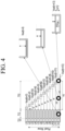
FIG. 4 illustrates the appearance of an image sensor of a global shutter method in which electric signals are sequentially output for each row line. -
FIG. 5 is a waveform diagram for the operation of a leakage compensation device according to the first embodiment. -
FIG. 6 illustrates a leakage compensation device according to the second embodiment. -
FIG. 7 is a waveform diagram for the operation of a leakage compensation device according to the second embodiment. -
FIG. 8 illustrates a leakage compensation device according to the third embodiment. -
FIG. 9 illustrates a leakage compensation device according to the fourth embodiment. -
FIG. 10 illustrates a leakage compensation device according to the fifth embodiment. -
FIG. 11 illustrates an image sensor according to the embodiment. - The sizes, shapes, numbers, etc. of the components shown in the drawings may differ from the actual ones. In addition, even if the same components are depicted in different sizes, shapes, and values between drawings, this is only an example in the drawings, and the same components may have the same sizes, shapes, and values between drawings.
- Hereinafter, the embodiments disclosed in this specification will be described in detail with reference to the attached drawings. Regardless of the drawing symbols, identical or similar components will be given the same reference numbers and redundant descriptions thereof will be omitted. The suffixes 'module' and 'part' used for components in the following description are given or used interchangeably in consideration of the ease of writing the specification, and do not have distinct meanings or roles in themselves. In addition, the attached drawings are intended to facilitate easy understanding of the embodiments disclosed in this specification, and the technical ideas disclosed in this specification are not limited by the attached drawings. In addition, when an element such as a layer, region, or substrate is mentioned as existing 'on' another element, this includes that it may be directly on the other element or that other intermediate elements may exist between them.
-
FIG. 1 illustrates a leakage compensation device according to a first embodiment. - The
leakage compensation device 100 according to the first embodiment may include apixel array 110, adetection circuit 130, etc. - The
pixel array 110 may includeM pixel circuits 120. TheM pixel circuits 120 may be arranged in a matrix form, for example, but are not limited thereto. - As illustrated in
FIG. 4 , thepixel array 110 may include a plurality of row lines (L1 to L12). Each of the row lines (L1 to L12) may include N (N<M) or more pixel circuits. - Meanwhile, the
leakage compensation device 100 according to the first embodiment may be operated as an image sensor of a global shutter method. As shown inFIG. 4 , the image sensor of the global shutter method may include a reset section (T11), a capture section (T12), an output section (T13), etc. The reset section (T11) may be called an initialization section, the capture section (T12) may be called a storage section, and the output section (T13) may be called a readout section. - During the reset section (T11),
M pixel circuits 120 may be reset. During the capture section (T12), electric signals (Vout(t=t1) to Vout(t=t12)) corresponding to light may be stored in theM pixel circuits 120. That is, an image of an object may be obtained during the capture section (T12). The electric signals (Vout(t=t1) to Vout(t=t12)) may be a current, a voltage, a potential, etc. - During the output section (T13), the electric signals (Vout(t=t1) to Vout(t=t12)) stored in the
M pixel circuits 120 may be sequentially output for each row line (L1 to L12). As shown inFIG. 4 , during the output section (T13), the electric signals (Vour(t-t1) to Vout(t=t12)) stored in theN pixel circuits 120 of each of the first to twelfth row lines (L1 to L12) may be output in the order of the first row line (L1), the second row line (L2), the third row line (L3), ..., the twelfth row line (L12). During the output section (T13), the M electric signals (Vout(t=t1) to Vout(t=t12)) consisting of an image of one frame may be output. - Since a readout line is commonly connected to the
pixel circuits 120 on the column lines, thepixel circuits 120 on the column lines can be driven by time division during the output section (T13). That is, during the output section (T13), the electric signals (Vout(t=t1) to Vout(t=t12)) stored in theN pixel circuits 120 included in each of the first to twelfth row lines (L1 to L12) can be output whenever a preset time elapses. For example, the electric signals (Vout(t=t1) to Vout(t=t12)) stored in theN pixel circuits 120 of the first row line (L1) can be output when a first time elapses, and the electric signals (Vout(t=t1) to Vout(t=t12)) stored in theN pixel circuits 120 of the second row line (L2) can be output when a second time elapses. The electric signals (Vout(t=t1) to Vout(t=t12)) stored in theN pixel circuits 120 of each of the remaining row lines (L3 to L12) can be output when the third to twelfth times elapse. - Meanwhile, the
detection circuit 130 can detect (or obtain) leakage signals (V(SD_monitor)) for compensating the output electric signals (Vout(t=t1) to Vout(t=t12)). The leakage signal (V(SD_monitor)) can be a current, a voltage, a potential, etc. formed by leaked charges, for example, electrons. - The
detection circuit 130 can be provided in thepixel array 110. Thedetection circuit 130 can be positioned corresponding to each of the plurality ofpixel circuits 120. For example, if thepixel array 110 is equipped with one millionpixel circuits 120, one milliondetection circuits 130 may also be equipped in thepixel array 110 corresponding to each of the one millionpixel circuits 120. - As will be described later, since the electric signals output from the pixel circuits are compensated based on the leakage signals that leak differently at different preset times, the output electric signals (Vout) are compensated for with the original electric signals using the leakage signals, so that the detection performance for the object can be improved.
- Meanwhile, the
pixel circuit 120 and thedetection circuit 130 may be commonly connected to the readout line (RO). In this case, the electric signal (Vout) of thepixel circuit 120 may be output through the readout line (RO) using time division, and then the leakage signal of thedetection circuit 130 may be output through the readout line (RO). The opposite operation may also be performed. - Referring to
FIGS. 2 and3 , thepixel circuit 120 and thedetection circuit 130 will be described in detail. - As shown in
FIG. 2 , thepixel circuit 120 may include a photodetector 120-1, an output circuit 120-2, etc. - The photodetector 120-1 may detect light and obtain an electric signal corresponding to the light. The photodetector 120-1 may be configured as a semiconductor light emitting diode.
- Although five transistors are shown in the output circuit 120-2 in
FIG. 2 , fewer or more transistors may be provided. - The output circuit 120-2 may include a first transistor (TFT11), a second transistor (TFT12), a third transistor (TFT13), a fourth transistor (TFT14), and a fifth transistor (TFT15). For example, the first transistor (TFT11) may be called a storage transistor, the second transistor (TFT12) may be called a transmission transistor, and the third transistor (TFT13) may be called a reset transistor. The fourth transistor (TFT14) may be called a driving transistor, and the fifth transistor (TFT15) may be called a selection transistor.
- The first transistor (TFT11) may be connected to a photodetector 120-1 and may store an electric signal obtained from the photodetector 120-1 in the storage capacitor (SD).
- The second transistor (TFT12) may be connected to the first transistor (TFT11) and may transmit and store an electric signal stored in the storage capacitor (SD) to the floating diffusion (FD).
- The third transistor (TFT13) may reset a node between the second transistor (TFT12) and the fourth transistor (TFT14).
- The fourth transistor (TFT14) can output an electric signal stored in a floating diffusion (FD). The fourth transistor (TFT14) can operate as a source-follower amplifier, but is not limited thereto.
- The fifth transistor (TFT15) is connected between the fourth transistor (TFT14) and the readout line (RO), and can output an electric signal (Vout) passing through the driving transistor to the readout line (RO).
- Meanwhile, the
pixel circuit 120 may further include a sixth transistor, a seventh transistor, etc. - The sixth transistor is connected between the photodetector 120-1 and the first transistor (TFT11), and can transmit and store an electric signal obtained from the photodetector 120-1 to a storage capacitor (SD). The sixth transistor may be called a transmission transistor.
- The seventh transistor may be commonly connected to the
M pixel circuits 120 of thepixel array 110 and may reset theM pixel circuits 120. For example, the seventh transistor may be provided in each of theM pixel circuits 120. For example, the seventh transistor may be provided outside theM pixel circuits 120 and may be commonly connected to theM pixel circuits 120. - As shown in
FIGS. 2 and3 , thedetection circuit 130 may have the same circuit structure as the circuit structure of the output circuit 120-2. - The
detection circuit 130 may detect a leakage signal (V(SD_monitor)). As described above, since the circuit structure of thedetection circuit 130 is the same as that of the output circuit 120-2, the leakage signal (V(SD_monitor)) may be the same as the value leaked from the electric signal of the output circuit 120-2. - Although five transistors are illustrated in the
detection circuit 130 inFIG. 3 , fewer or more transistors may be provided. - The
detection circuit 130 may include a first transistor (TFT21), a second transistor (TFT22), a third transistor (TFT23), a fourth transistor (TFT24), and a fifth transistor (TFT25). For example, the first transistor (TFT21) may be called a monitoring transistor, the second transistor (TFT22) may be called a transmission transistor, and the third transistor (TFT23) may be called a reset transistor. The fourth transistor (TFT24) may be called a driving transistor, and the fifth transistor (TFT25) may be called a selection transistor. - The first transistor (TFT21) may monitor a leakage signal (V(SD_monitor)) for a preset section of time and store it in a storage capacitor (SD_monitor).
- The second transistor (TFT22) may be connected to the first transistor (TFT21) and may transmit and store the leakage signal (V(SD_monitor)) stored in the monitoring storage capacitor (SD_monitor) to a floating diffusion (FD).
- The third transistor (TFT23) may reset a node between the second transistor (TFT22) and the fourth transistor (TFT24).
- The fourth transistor (TFT24) may output the leakage signal (V(SD_monitor)) stored in the floating diffusion (FD). The fourth transistor (TFT24) can be operated as a source-follower amplifier, but is not limited thereto.
- The fifth transistor (TFT25) is connected between the fourth transistor (TFT24) and the readout line (RO), and can output a leakage signal (V(SD_monitor)) via the driving transistor to the readout line (RO).
- Meanwhile, unlike
FIG. 3 , the first transistor (TFT21) is omitted, and the storage capacitor (SD_monitor) can be directly connected to the second transistor (TFT22). In this case, the leakage signal (V(SD_monitor)) stored in the storage capacitor (SD_monitor) can be transmitted to the floating diffusion (FD) via the second transistor (TFT22). - The operation of the leakage compensation device is explained with reference to
FIGS. 1 to 5 . - As shown in
FIG. 4 , it can be operated by dividing into a reset section (T11), a capture section (T12), and an output section (T13). The reset section (T11), the capture section (T12), and the output section (T13) can be defined as one cycle. This cycle can correspond to one frame or be a part of one frame. - As shown in
FIGS. 4 and5 , during the reset section (T11),M pixel circuits 120 can be reset. For example, the seventh transistor can be turned on by the overflow drain signal (OG), andM pixel circuits 120 of thepixel array 110 can be reset. - As shown in
FIG. 4 andFIG. 5 , during the capture section (T12), electric signals corresponding to light (Vout (t=t1) to Vout (t=t12)) are stored inM pixel circuits 120, so that an image of an object can be obtained. - During the capture section (T12), the third transistor (TFT13) of the
pixel circuit 120 and the third transistor (TFT23) of thedetection circuit 130 are turned on by the first reset signal (RES1) and the second reset signal (RES2), respectively, so that the node of thepixel circuit 120 and the node of thedetection circuit 130 can be reset. InFIG. 1 , since thepixel circuit 120 and thedetection circuit 130 are connected to the same readout line (RO), the node of thepixel circuit 120 and the node of thedetection circuit 130 may be reset at different times. That is, after the fifth transistor (TFT15) is turned on by the first selection signal in thepixel circuit 120 and the node is reset through the readout line (RO), the fifth transistor (TFT25) may be turned on by the second selection circuit in thedetection circuit 130 and the node may be reset through the readout line (RO). - Meanwhile, in the
pixel circuit 120, the sixth transistor and the first transistor (TFT11) may be turned on by the first transmission signal (TX1) and the storage gate signal (SG), respectively, so that an electric signal corresponding to light detected by the photodetector 120-1 may be stored in the storage capacitor (SD). In thedetection circuit 130, the leakage signal (V(SD_monitor)) may be stored in the storage capacitor (SD_monitor) by the storage monitoring gate signal (SG_monitor). - Afterwards, in the
pixel circuit 120, the second transistor (TFT12) is turned on by the second transmission signal (TX2), so that the electric signal stored in the storage capacitor (SD) may be transmitted and stored in the floating diffusion (FD). In thedetection circuit 130, the second transistor (TFT22) is turned on by the transmission signal (TX2), so that the leakage signal (V(SD_monitor)) stored in the storage capacitor (SD_monitor) may be transmitted and stored in the floating diffusion (FD). - As shown in
FIG. 4 andFIG. 5 , during the output section (T13), the electric signals (Vout (t=t1) to Vout (t=t12)) stored in theM pixel circuits 120 can be sequentially output for each row line (L1 to L12). - In
FIG. 1 , since thepixel circuit 120 and thedetection circuit 130 are connected to the same readout line (RO), the output timing of the electric signal (Vout) of thepixel circuit 120 and the leakage signal (V (SD_monitor)) of thedetection circuit 130 can be different. That is, in thepixel circuit 120, the fifth transistor (TFT15) is turned on by the first selection signal, and the electric signal (Vout) stored in the floating diffusion (FD) is output through the readout line (RO), and then in thedetection circuit 130, the fifth transistor (TFT25) is turned on by the second selection circuit, and the leakage signal (V(SD_monitor)) stored in the floating diffusion (FD) can be output through the readout line (RO). - As described above, as shown in
FIGS. 2 and3 , since thepixel circuit 120 and thedetection circuit 130 are commonly connected to the same readout line (RO), the electric signal (Vout) and the leakage signal (V(SD_monitor)) can be output (or obtained) at different times. That is, as illustrated in 5, the electric signal (Vout) stored in thepixel circuit 120 may be output first, and then the leakage signal (V(SD_monitor)) stored in thedetection circuit 130 may be output. - Meanwhile, the time at which the electric signal is stored and then output in each
pixel circuit 120 may be determined by a preset time. As shown inFIG. 4 , the preset times (t1 to t12) may be different for each row line (L1 to L12). Accordingly, the leakage value in the corresponding electric signal (Vout(t=t1) to Vout(t=t12)) may be different for each row line (L1 to L12). For example, the longer the preset time (t1 to t12), the more different the leakage value in the corresponding electric signal (Vout(t=t1) to Vout(t=t12)) may be. - The electric signal (Vout(t=t1) to Vout(t=t12)) output from the
pixel circuit 120 at a preset time (t1 to t12) may be a value reduced by the value leaked during the preset time (t1 to t12) from the electric signal stored in the floating diffusion (FD). That is, the electric signal stored in the floating diffusion may be reduced by the value leaked during the preset time (t1 to t12) and output through the readout line (RO). For example, as shown inFIG. 4 , among theN pixel circuits 120 on the 12th row line (L12), the first pixel circuit may be stored as an electric signal during the capture section (T12). The electric signal stored in the first pixel circuit may be reduced by the leaked value (LV12) during the first time (t12). Accordingly, the electric signal stored in the first pixel circuit can be output to the readout line (RO) as a value reduced by [Vout(t=0) - LV12] when the first time (t12) elapses. - For example, the electric signals (Vout(t=t5)) output from the
N pixel circuits 120 on the fifth row line (L5) can have a larger leakage amount than the electric signals (Vout(t=t1)) output from theN pixel circuits 120 on the first row line (L1). For example, the electric signals (Vout(t=t12)) output from theN pixel circuits 120 on the twelfth row line (L12) can have a larger leakage amount than the electric signals (Vout(t=t7)) output from theN pixel circuits 120 on the seventh row line (L7). - According to an embodiment, by detecting a leakage signal (V(SD_monitor)) that is equal to a value leaked from an electric signal of a
pixel circuit 120 in adetection circuit 130, an electric signal (Vout) output from apixel circuit 120 can be compensated based on the leakage signal (V(SD_monitor)). Accordingly, an original electric signal before leakage is obtained, so that loss of image data is prevented, and detection performance for an object can be improved. -
FIG. 6 illustrates a leakage compensation device according to the second embodiment. - The second embodiment is the same as the first embodiment except that the
pixel circuit 120 and thedetection circuit 130 are independently connected to the first readout line (RO1) and the second readout line (RO2), respectively. In the second embodiment, the same drawing reference numerals are given to components having the same structure or function as those of the first embodiment, and detailed descriptions are omitted. - Referring to
FIG. 6 , theleakage compensation device 100A according to the second embodiment may include apixel array 110, adetection circuit 130, etc. - The
pixel array 110 may includeM pixel circuits 120. Adetection circuit 130 may be provided corresponding to each of theM pixel circuits 120. That is, theM detection circuits 130 may be provided. In this case, thepixel circuit 120 may be connected to the first readout line (RO1), and thedetection circuit 130 may be connected to the second readout line (RO2). In this way, since thepixel circuit 120 and thedetection circuit 130 are connected to different readout lines (RO1, RO2), the electric signal (Vout) stored in thepixel circuit 120 and the leakage signal (V(SD_monitor)) stored in thedetection circuit 130 may be individually output. For example, the electric signal (Vout) and the leakage signal (V(SD_monitor)) may be output simultaneously or differently. - As illustrated in
FIG. 2 andFIG. 7 , the fifth transistor (TFT15) of thepixel circuit 120 and the fifth transistor (TFT25) of thedetection circuit 130 are turned on at the same time by the first selection signal and the second selection signal, respectively, so that the electric signal (Vout) stored in thepixel circuit 120 and the leakage signal (V(SD_monitor)) stored in thedetection circuit 130 can be simultaneously output through the first readout line (RO1) and the second readout line (RO2), respectively. -
FIG. 8 illustrates a leakage compensation device according to the third embodiment. - The third embodiment is the same as the first embodiment and/or the second embodiment, except that the
detection circuit 130 is located within thepixel circuit 120. In the third embodiment, the same drawing reference numerals are given to components having the same structure or function as those of the first embodiment and/or the second embodiment, and detailed descriptions are omitted. - Referring to
FIG. 8 , aleakage compensation device 100B according to the third embodiment may include apixel array 110, adetection circuit 130, etc. - The
pixel array 110 may includeM pixel circuits 120. Adetection circuit 130 may be provided corresponding to each of theM pixel circuits 120. That is,M detection circuits 130 may be provided. - The
detection circuit 130 may be located within thepixel circuit 120. For example, thedetection circuit 130 may be physically located within thepixel circuit 120 or may be circuitically included within thepixel circuit 120. For example, thedetection circuit 130 illustrated inFIG. 3 may be included in thepixel circuit 120 illustrated inFIG. 2 . In this case, thedetection circuit 130 may be located within the area where thepixel circuit 120 is formed. For example, thepixel circuit 120 and thedetection circuit 130 may be commonly connected to a line that shares a power supply (VDDP). -
FIG. 9 illustrates a leakage compensation device according to the fourth embodiment. - The fourth embodiment is similar to the first to third embodiments except that the
detection circuit 130 is arranged adjacent to at least two ormore pixel circuits 121 to 124. In the fourth embodiment, the same drawing reference numerals are given to components having the same structure or function as those of the first to third embodiments, and detailed descriptions are omitted. - Referring to
FIG. 9 , theleakage compensation device 100C according to the fourth embodiment may include apixel array 110, adetection circuit 130, etc. - The
pixel array 110 may includeM pixel circuits 120. Thedetection circuit 130 may be arranged adjacent to at least twopixel circuits 121 to 124. For example, thedetection circuit 130 may be surrounded by at least twopixel circuits 121 to 124, but is not limited thereto. - For example, the
detection circuit 130 may be surrounded by fourpixel circuits 121 to 124, but is not limited thereto. Thedetection circuit 130 may be located in a central region of an area composed of fourpixel circuits 121 to 124. - Four
pixel circuits 121 to 124 may be connected to the first readout line (RO1), and thedetection circuit 130 may be connected to the second readout line (RO2). - For example, the four
pixel circuits 121 to 124 may sequentially output electric signals through the first readout line (RO1) using time division. - For example, the
detection circuit 130 may sequentially output a leakage signal through the second readout line (RO2) as many times as the number ofpixel circuits 121 to 124 using time division. - For example, the detection signal may output the first leakage signal when the electric signal of the
first pixel circuit 121 is output. The first leakage signal may be the same as the value leaked from the electric signal of thefirst pixel circuit 121. For example, the detection signal may output a second leakage signal when the electric signal of thesecond pixel circuit 122 is output. The second leakage signal may be the same as the value leaked from the electric signal of thesecond pixel circuit 122. For example, the detection signal may output a third leakage signal when the electric signal of thethird pixel circuit 123 is output. The third leakage signal may be the same as the value leaked from the electric signal of thethird pixel circuit 123. For example, the detection signal may output a fourth leakage signal when the electric signal of thefourth pixel circuit 124 is output. The fourth leakage signal may be the same as the value leaked from the electric signal of thefourth pixel circuit 124. - Although not shown, four
pixel circuits 121 to 124 and thedetection circuit 130 may be commonly connected to the same readout line. -
FIG. 10 illustrates a leakage compensation device according to a fifth embodiment. - The fifth embodiment is similar to the first to third embodiments except that the
detection circuit 130 is located around thepixel array 110. In the fourth embodiment, the same reference numerals are given to components having the same structure or function as those of the first to fourth embodiments, and detailed descriptions are omitted. - Referring to
FIG. 10 , theleakage compensation device 100D according to the fifth embodiment may include apixel array 110, adetection circuit 130, etc. - The
pixel array 110 may includeM pixel circuits 120. Thedetection circuit 130 may be located around thepixel array 110. - At least one
dummy pixel region 151 to 154 may be positioned around thepixel array 110. Thedummy pixel region 151 to 154 may include a plurality of pixel circuits, but the pixel circuits may not operate. - For example, four
dummy pixel regions 151 to 154 may be positioned around thepixel array 110. - Meanwhile, in an embodiment, the
detection circuit 130 may be provided at at least one location of at least onedummy pixel region 151 to 154. - For example, two detection circuits 130 (131a to 131c, 132a to 132c, 133a to 133c, 134a to 134c) may be positioned in each of four dummy pixel regions (151 to 154).
- The electric signals of the N pixel circuits of the row line can be corrected using the detection signals detected by the detection circuits 130 (131a to 131c, 132a to 132c, 133a to 133c, 134a to 134c) positioned in each of four dummy pixel regions (151 to 154). For example, the electric signals of the N pixel circuits of the row line may be corrected using the detection signals using an interpolation method.
- Although not shown, two detection circuits 130 (132a to 132c, 1341, 134b) may be positioned in each of the second
dummy pixel area 152 and the fourthdummy pixel area 154, and nodetection circuit 130 may be positioned in the firstdummy pixel area 151 and the thirddummy pixel area 153. - Although not shown, two detection circuits 130 (131a to 131c, 1331, 133b) may be positioned in each of the first
dummy pixel area 151 and the thirddummy pixel area 153, and nodetection circuit 130 may be positioned in the seconddummy pixel area 152 and the fourthdummy pixel area 154. - Although not shown, the
detection circuits 130 may be located only in one of the firstdummy pixel area 151 and the thirddummy pixel area 153. -
FIG. 11 illustrates an image sensor according to an embodiment. Although the leakage compensation device according to the first embodiment (FIGS. 1 to 5 ) is illustrated in the drawing, the leakage compensation device according to the second to fifth embodiments (FIGS. 6 ,8 to 10 ) may also be included in the image sensor according to the embodiment. - Referring to
FIG. 11 , theimage sensor 200 according to the embodiment may include apixel array 110, adetection circuit 130, acorrection circuit 210, etc. - Since the
pixel array 110 and thedetection circuit 130 have been described in the first embodiment (FIG. 1 ), a detailed description thereof will be omitted. - Each of the
M pixel circuits 120 included in thepixel array 110 may include a photodetector 120-1 and an output circuit 120-2. - The
correction circuit 210 may correct the electric signals (Vout) output from the plurality ofpixel circuits 120 using the leakage signals (V(SD_monitor)) output from thedetection circuit 130. - As illustrated in
FIG. 4 , the electric signals (Vout(t=t1) to Vout(t=t12)) of thepixel circuits 120 on the row lines (L1 to L12) may be sequentially output for each row line (L1 to L12) whenever a preset time (t1 to t12) elapses for each row line (L1 to L12). Accordingly, the electric signals (Vout(t=t1) to Vout(t=t12)) output by row line (L1 to L12) can be reduced by the value leaked during the preset time (t1 to t12). - The
detection circuit 130 may have the same circuit structure as the circuit structure of the output circuit 120-2. Accordingly, the leakage signal (V(SD_monitor)) detected by thedetection circuit 130 may be the same as the value leaked during the preset time (t1 to t12) in the electric signal of thecorresponding pixel circuit 120. - Referring again to
FIG. 11 , thecorrection circuit 210 may convert the electric signals (Vout) into digital signals to obtain sensing data. Thecorrection circuit 210 may convert the leakage signals (V(SD_monitor)) into digital signals to obtain leakage data. - The
correction circuit 210 can obtain original sensing data by performing an operation of adding the leakage data to each sensing data. The original sensing data may be data on electric signals before leakage. - According to the embodiment, the original sensing data corrected using the leakage data does not have a loss due to the leakage, so that an accurate image of the object can be obtained using the original sensing data, thereby improving the detection performance of the object.
- The above detailed description should not be construed as limiting in all aspects and should be considered as illustrative. The scope of the embodiment should be determined by a reasonable interpretation of the appended claims, and all changes within the equivalent scope of the embodiment are included in the scope of the embodiment.
Claims (15)
- A leakage compensation device comprising:a pixel array including a plurality of row lines each including a plurality of pixel circuits, configured to store electric signals corresponding to light in the plurality of pixel circuits during a capture section, and sequentially output the stored electric signals by row line whenever a preset time elapses for each row line during an output section; anda plurality of detection circuits configured to detect leakage signals for compensating the outputted electric signals.
- The leakage compensation device of claim 1, wherein the pixel circuit includes:a photodetector configured to detect the light; andan output circuit configured to store and output the electric signal corresponding to the detected light.
- The leakage compensation device of claim 2, wherein the detection circuit has the same circuit structure as a circuit structure of the output circuit.
- The leakage compensation device of any one of the preceding claims, wherein each of the outputted electric signals is a value reduced by the value leaked during the preset time from each of the stored electric signals.
- The leakage compensation device of claim 4, wherein the leakage signal is the same as the leaked value.
- The leakage compensation device of any one of the preceding claims, wherein the electric signal and the leakage signal are output simultaneously or differently.
- The leakage compensation device of any one of the preceding claims, wherein the detection circuit is positioned within the pixel circuit.
- The leakage compensation device of any one of the preceding claims, wherein the detection circuit is located corresponding to the pixel circuit.
- The leakage compensation device of claim 7, further comprises a readout line commonly connected to the pixel circuit and the detection circuit.
- The leakage compensation device of any one of the preceding claims, wherein the detection circuit is arranged adjacent to at least two or more pixel circuits to detect a leakage signal of each of the at least two or more pixel circuits.
- The leakage compensation device of claim 10, further comprising:a first readout line commonly connected to the at least two pixel circuits; anda second readout line connected to the detection circuit.
- The leakage compensation device of any one of the preceding claims, further comprises at least one dummy pixel area around the pixel array, andwherein the detection circuit is provided at at least one position of the at least one dummy pixel area.
- An image sensor comprising:a pixel array including a plurality of row lines each including a plurality of pixel circuits, configured to store electric signals corresponding to light in the plurality of pixel circuits during a capture section, and sequentially output the stored electric signals by row line whenever a preset time elapses for each row line during an output section; anda plurality of detection circuits configured to detect leakage signals from the electric signals of the pixel circuit.
- The image sensor of claim 13, further comprises a correction circuit configured to correct the outputted electric signals using the leakage signals.
- The image sensor of claim 13, further comprises a correction circuit configured to correct the electric signals outputted from the pixel circuits based on the leakage signals that are leaked differently at different preset times.
Applications Claiming Priority (2)
| Application Number | Priority Date | Filing Date | Title |
|---|---|---|---|
| KR20230175452 | 2023-12-06 | ||
| KR1020240086554A KR20250086471A (en) | 2023-12-06 | 2024-07-02 | Leakage correction device and image sensor |
Publications (1)
| Publication Number | Publication Date |
|---|---|
| EP4568267A1 true EP4568267A1 (en) | 2025-06-11 |
Family
ID=93842001
Family Applications (1)
| Application Number | Title | Priority Date | Filing Date |
|---|---|---|---|
| EP24217945.5A Pending EP4568267A1 (en) | 2023-12-06 | 2024-12-06 | Leakage correction device and image sensor |
Country Status (3)
| Country | Link |
|---|---|
| US (1) | US20250193371A1 (en) |
| EP (1) | EP4568267A1 (en) |
| TW (1) | TW202527564A (en) |
Citations (3)
| Publication number | Priority date | Publication date | Assignee | Title |
|---|---|---|---|---|
| US20090021622A1 (en) * | 2007-07-17 | 2009-01-22 | Olympus Corporation | Solid-state imaging apparatus |
| US20120126097A1 (en) * | 2005-05-17 | 2012-05-24 | Canon Kabushiki Kaisha | Image sensing device using a photoelectric converter and a control method therefor |
| US20200221043A1 (en) * | 2017-08-02 | 2020-07-09 | Sony Semiconductor Solutions Corporation | Solid-state imaging element and imaging apparatus |
Family Cites Families (2)
| Publication number | Priority date | Publication date | Assignee | Title |
|---|---|---|---|---|
| US8836835B2 (en) * | 2010-10-04 | 2014-09-16 | International Business Machines Corporation | Pixel sensor cell with hold node for leakage cancellation and methods of manufacture and design structure |
| WO2020230610A1 (en) * | 2019-05-15 | 2020-11-19 | 富士フイルム株式会社 | Leakage light detection device, imaging device, leakage light detection method, and leakage light detection program |
-
2024
- 2024-12-06 TW TW113147522A patent/TW202527564A/en unknown
- 2024-12-06 US US18/971,173 patent/US20250193371A1/en active Pending
- 2024-12-06 EP EP24217945.5A patent/EP4568267A1/en active Pending
Patent Citations (3)
| Publication number | Priority date | Publication date | Assignee | Title |
|---|---|---|---|---|
| US20120126097A1 (en) * | 2005-05-17 | 2012-05-24 | Canon Kabushiki Kaisha | Image sensing device using a photoelectric converter and a control method therefor |
| US20090021622A1 (en) * | 2007-07-17 | 2009-01-22 | Olympus Corporation | Solid-state imaging apparatus |
| US20200221043A1 (en) * | 2017-08-02 | 2020-07-09 | Sony Semiconductor Solutions Corporation | Solid-state imaging element and imaging apparatus |
Also Published As
| Publication number | Publication date |
|---|---|
| US20250193371A1 (en) | 2025-06-12 |
| TW202527564A (en) | 2025-07-01 |
Similar Documents
| Publication | Publication Date | Title |
|---|---|---|
| US6876353B2 (en) | Shift register and electronic apparatus | |
| US7924249B2 (en) | Method and system for light emitting device displays | |
| US11636789B2 (en) | Pixel unit, array substrate, display panel, display apparatus, and detection method of pixel circuit | |
| US9626035B2 (en) | OLED pixel circuit, driving method thereof and display panel | |
| US8759739B2 (en) | Optical sensor and display apparatus | |
| US20210201774A1 (en) | Shift register unit, gate driving circuit, display device and driving method | |
| US20220028340A9 (en) | Shift register unit, gate driving circuit, display device and driving method | |
| KR100932205B1 (en) | A pixel circuit, a display device including the same, and a method of operating the pixel circuit | |
| US11348518B2 (en) | Method for driving display panel and display device | |
| US20040189611A1 (en) | Signal detector | |
| WO2011104957A1 (en) | Display device | |
| US20210325987A1 (en) | Pixel circuit and drive method thereof, and touch display apparatus | |
| US8822939B2 (en) | Matrix substrate, detection device, detection system, and method for driving detection device | |
| US20220013060A1 (en) | Shift Register and Drive Method Therefor, and Gate Drive Circuit | |
| US8803791B2 (en) | Display device | |
| JP2005251348A (en) | Shift register circuit and drive control method thereof | |
| US11151945B2 (en) | Organic light emitting diode display device and control method thereof | |
| US20110315859A1 (en) | Display device | |
| US8300125B2 (en) | Method and apparatus for using thin-film transistors and MIS capacitors as light-sensing elements in charge mapping arrays | |
| US7342410B2 (en) | Display device and pixel testing method thereof | |
| US20110096049A1 (en) | Display device | |
| US20240290233A1 (en) | Control method and control device for current detection apparatus | |
| US20110102393A1 (en) | Display device | |
| US20250193371A1 (en) | Leakage correction device and image sensor | |
| EP2562625A1 (en) | Display with touch-sensor |
Legal Events
| Date | Code | Title | Description |
|---|---|---|---|
| PUAI | Public reference made under article 153(3) epc to a published international application that has entered the european phase |
Free format text: ORIGINAL CODE: 0009012 |
|
| STAA | Information on the status of an ep patent application or granted ep patent |
Free format text: STATUS: THE APPLICATION HAS BEEN PUBLISHED |
|
| AK | Designated contracting states |
Kind code of ref document: A1 Designated state(s): AL AT BE BG CH CY CZ DE DK EE ES FI FR GB GR HR HU IE IS IT LI LT LU LV MC ME MK MT NL NO PL PT RO RS SE SI SK SM TR |
|
| STAA | Information on the status of an ep patent application or granted ep patent |
Free format text: STATUS: REQUEST FOR EXAMINATION WAS MADE |
|
| 17P | Request for examination filed |
Effective date: 20251209 |
|
| STAA | Information on the status of an ep patent application or granted ep patent |
Free format text: STATUS: EXAMINATION IS IN PROGRESS |
|
| 17Q | First examination report despatched |
Effective date: 20260511 |