EP4568196A1 - A differential input receiver and a wake-up receiver - Google Patents
A differential input receiver and a wake-up receiver Download PDFInfo
- Publication number
- EP4568196A1 EP4568196A1 EP24156391.5A EP24156391A EP4568196A1 EP 4568196 A1 EP4568196 A1 EP 4568196A1 EP 24156391 A EP24156391 A EP 24156391A EP 4568196 A1 EP4568196 A1 EP 4568196A1
- Authority
- EP
- European Patent Office
- Prior art keywords
- fet
- source
- terminal
- differential
- gate
- Prior art date
- Legal status (The legal status is an assumption and is not a legal conclusion. Google has not performed a legal analysis and makes no representation as to the accuracy of the status listed.)
- Pending
Links
Images



Classifications
-
- H—ELECTRICITY
- H04—ELECTRIC COMMUNICATION TECHNIQUE
- H04L—TRANSMISSION OF DIGITAL INFORMATION, e.g. TELEGRAPHIC COMMUNICATION
- H04L25/00—Baseband systems
- H04L25/02—Details ; arrangements for supplying electrical power along data transmission lines
- H04L25/0264—Arrangements for coupling to transmission lines
- H04L25/0272—Arrangements for coupling to multiple lines, e.g. for differential transmission
-
- H—ELECTRICITY
- H04—ELECTRIC COMMUNICATION TECHNIQUE
- H04B—TRANSMISSION
- H04B1/00—Details of transmission systems, not covered by a single one of groups H04B3/00 - H04B13/00; Details of transmission systems not characterised by the medium used for transmission
- H04B1/06—Receivers
- H04B1/16—Circuits
- H04B1/1607—Supply circuits
-
- H—ELECTRICITY
- H04—ELECTRIC COMMUNICATION TECHNIQUE
- H04L—TRANSMISSION OF DIGITAL INFORMATION, e.g. TELEGRAPHIC COMMUNICATION
- H04L12/00—Data switching networks
- H04L12/28—Data switching networks characterised by path configuration, e.g. LAN [Local Area Networks] or WAN [Wide Area Networks]
- H04L12/40—Bus networks
- H04L12/40006—Architecture of a communication node
-
- H—ELECTRICITY
- H03—ELECTRONIC CIRCUITRY
- H03K—PULSE TECHNIQUE
- H03K17/00—Electronic switching or gating, i.e. not by contact-making and –breaking
- H03K17/22—Modifications for ensuring a predetermined initial state when the supply voltage has been applied
- H03K17/223—Modifications for ensuring a predetermined initial state when the supply voltage has been applied in field-effect transistor switches
-
- H—ELECTRICITY
- H03—ELECTRONIC CIRCUITRY
- H03K—PULSE TECHNIQUE
- H03K3/00—Circuits for generating electric pulses; Monostable, bistable or multistable circuits
- H03K3/01—Details
- H03K3/012—Modifications of generator to improve response time or to decrease power consumption
-
- H—ELECTRICITY
- H04—ELECTRIC COMMUNICATION TECHNIQUE
- H04L—TRANSMISSION OF DIGITAL INFORMATION, e.g. TELEGRAPHIC COMMUNICATION
- H04L12/00—Data switching networks
- H04L12/02—Details
- H04L12/12—Arrangements for remote connection or disconnection of substations or of equipment thereof
-
- H—ELECTRICITY
- H04—ELECTRIC COMMUNICATION TECHNIQUE
- H04L—TRANSMISSION OF DIGITAL INFORMATION, e.g. TELEGRAPHIC COMMUNICATION
- H04L12/00—Data switching networks
- H04L12/28—Data switching networks characterised by path configuration, e.g. LAN [Local Area Networks] or WAN [Wide Area Networks]
- H04L12/40—Bus networks
- H04L12/40006—Architecture of a communication node
- H04L12/40039—Details regarding the setting of the power status of a node according to activity on the bus
-
- H—ELECTRICITY
- H04—ELECTRIC COMMUNICATION TECHNIQUE
- H04L—TRANSMISSION OF DIGITAL INFORMATION, e.g. TELEGRAPHIC COMMUNICATION
- H04L25/00—Baseband systems
- H04L25/02—Details ; arrangements for supplying electrical power along data transmission lines
- H04L25/0264—Arrangements for coupling to transmission lines
- H04L25/0292—Arrangements specific to the receiver end
-
- H—ELECTRICITY
- H04—ELECTRIC COMMUNICATION TECHNIQUE
- H04L—TRANSMISSION OF DIGITAL INFORMATION, e.g. TELEGRAPHIC COMMUNICATION
- H04L25/00—Baseband systems
- H04L25/02—Details ; arrangements for supplying electrical power along data transmission lines
- H04L25/08—Modifications for reducing interference; Modifications for reducing effects due to line faults ; Receiver end arrangements for detecting or overcoming line faults
- H04L25/085—Arrangements for reducing interference in line transmission systems, e.g. by differential transmission
-
- H—ELECTRICITY
- H03—ELECTRONIC CIRCUITRY
- H03K—PULSE TECHNIQUE
- H03K3/00—Circuits for generating electric pulses; Monostable, bistable or multistable circuits
- H03K3/02—Generators characterised by the type of circuit or by the means used for producing pulses
- H03K3/353—Generators characterised by the type of circuit or by the means used for producing pulses by the use, as active elements, of field-effect transistors with internal or external positive feedback
- H03K3/356—Bistable circuits
- H03K3/356104—Bistable circuits using complementary field-effect transistors
- H03K3/356113—Bistable circuits using complementary field-effect transistors using additional transistors in the input circuit
- H03K3/35613—Bistable circuits using complementary field-effect transistors using additional transistors in the input circuit the input circuit having a differential configuration
-
- H—ELECTRICITY
- H03—ELECTRONIC CIRCUITRY
- H03K—PULSE TECHNIQUE
- H03K5/00—Manipulating of pulses not covered by one of the other main groups of this subclass
- H03K5/22—Circuits having more than one input and one output for comparing pulses or pulse trains with each other according to input signal characteristics, e.g. slope, integral
- H03K5/24—Circuits having more than one input and one output for comparing pulses or pulse trains with each other according to input signal characteristics, e.g. slope, integral the characteristic being amplitude
- H03K5/2472—Circuits having more than one input and one output for comparing pulses or pulse trains with each other according to input signal characteristics, e.g. slope, integral the characteristic being amplitude using field effect transistors
- H03K5/2481—Circuits having more than one input and one output for comparing pulses or pulse trains with each other according to input signal characteristics, e.g. slope, integral the characteristic being amplitude using field effect transistors with at least one differential stage
-
- H—ELECTRICITY
- H04—ELECTRIC COMMUNICATION TECHNIQUE
- H04L—TRANSMISSION OF DIGITAL INFORMATION, e.g. TELEGRAPHIC COMMUNICATION
- H04L12/00—Data switching networks
- H04L12/28—Data switching networks characterised by path configuration, e.g. LAN [Local Area Networks] or WAN [Wide Area Networks]
- H04L12/40—Bus networks
- H04L2012/40208—Bus networks characterized by the use of a particular bus standard
- H04L2012/40215—Controller Area Network CAN
Definitions
- the present disclosure relates to a differential input receiver and a wake-up receiver, and in particular to such receivers for a CAN system.
- a differential input receiver for detecting wake-up signalling in a differential communication system, the receiver comprising:
- the differential input receiver further comprises:
- the differential input receiver further comprises:
- the differential input receiver further comprises a threshold resistor connected between either:
- the differential input receiver further comprises a threshold setting current source configured to provide a current to a node between either:
- the differential input receiver further comprises:
- the differential input receiver further comprises:
- the differential input receiver further comprises:
- a wake-up receiver comprising:
- the wake-up receiver further comprises an additional gain stage comprising:
- Examples disclosed herein address supply headroom limitations of a wake-up receiver (WURX) at low supply voltages. They can also provide excellent electromagnetic compatibility (EMC) immunity, speed and low quiescent current consumption.
- EMC electromagnetic compatibility
- the present disclosure relates to differential communication systems, such as CAN (Controller Area Network) systems. It is known for CAN systems to be used in automobiles, which is an environment where a reasonable amount of noise can be present.
- CAN Controller Area Network
- a wake-up receiver is a low power circuit that is intended to detect a wake-up pattern or tone on a bus when a main analogue supply voltage (VCC) is off for power saving. Therefore, the current consumption of the WURX should be low.
- wake-up signalling is provided as a differential signal on a bus with a defined amplitude and frequency.
- the wake-up signalling on the bus can be present amidst high RF (radio frequency) common mode DPI (direct power injection); which can be as much as 25 V to 40 V, at frequencies in excess of 1 MHz.
- DPI direct power injection
- the supply voltage for the wake-up receiver is much smaller than the DPI noise amplitudes.
- a resistive divider with a large division ratio can be used to provide a voltage signal for wake-up detection that is much lower than the voltage level on the bus. This can assist with high DPI and supply headroom requirements. Additionally, BJT (bipolar junction transistor) and diode-based class A differential comparators can be used to reject common mode noise and detect a wake-up.
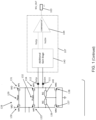
- Figure 1 shows an example embodiment of a wake-up receiver 100 for a CAN system according to an aspect of the present disclosure.
- the CAN system is an example of a differential communication system, which has a positive bus (Bus+) 101 and a negative bus (Bus-) 102.
- the wake-up receiver 100 has a wake-up receiver output terminal 103, which provides a wake-up receiver output signal.
- the wake-up receiver 100 includes:
- the first resistive divider 104, the second resistive divider 105 and the cross-coupled differential amplifier 106 can together be considered as a differential input receiver 110.
- the differential input receiver 110 has:
- the pre-amplifier and the comparator 107 are connected to the first and second output terminals 111, 112 of the differential input receiver 110.
- the first resistive divider 104 is connected to the positive bus (Bus+) 101. It is used to attenuate the common mode voltages on the positive bus (Bus+) 101 to acceptable levels such that the output voltage of the first resistive divider 104 can be used for signal processing by the downstream components of the wake-up receiver 100.
- the second resistive divider 105 is connected to the negative bus (Bus-) 102.
- the first resistive divider 104 includes a first upper voltage divider resistor (RU) 113 and a first lower voltage divider resistor (RL) 114.
- the first upper voltage divider resistor (RU) 113 has: a first terminal, which is connected to the positive input signal terminal 108; and a second terminal, which is connected to the cross-coupled differential amplifier 106 (as will be discussed below).
- the first lower voltage divider resistor (RL) 114 has: a first terminal, which is connected to the second terminal of the first upper voltage divider resistor (RU) 113; and a second terminal, which is connected to a ground terminal 117.
- the second resistive divider 105 includes a second upper voltage divider resistor (RU) 115 and a second lower voltage divider resistor (RL) 116.
- the second upper voltage divider resistor (RU) 115 has: a first terminal, which is connected to the negative input signal terminal 109; and a second terminal, which is connected to the cross-coupled differential amplifier 106 (as will be discussed below).
- the second lower voltage divider resistor (RL) 116 has: a first terminal, which is connected to the second terminal of the second upper voltage divider resistor (RU) 115; and a second terminal, which is connected to the ground terminal 117.
- Each of the first and second upper voltage divider resistors (RU) 113, 115 has a resistance value that is greater than the resistance value of its associated lower voltage divider resistor (RL) 114, 116.
- the resistance of an upper voltage divider resistor (RU) 113, 115 may be an order of magnitude greater than the resistance of its associated lower voltage divider resistor (RL) 114, 116. It will be appreciated that the ratio of RU/RL defines the division ratio of the BUS signal for DPI common mode management.
- the first resistive divider 104 also includes a first capacitor 118.
- the first capacitor 118 has a first plate and a second plate. The first plate is connected to the second terminal of the first upper voltage divider resistor (RU) 113. The second plate is connected to the ground terminal 117. In this way, the first capacitor 118 is connected in parallel with the first lower voltage divider resistor (RL) 114.
- the second resistive divider 105 includes a second capacitor 119.
- the second capacitor has a first plate and a second plate. The first plate is connected to the second terminal of the second upper voltage divider resistor (RU) 115. The second plate is connected to the ground terminal 117. In this way, the second capacitor 119 is connected in parallel with the second lower voltage divider resistor (RL) 116.
- the combination of the lower voltage divider resistor (RL) 114, 116 RL and the associated capacitor 118, 119 form the pole of a low pass filter. This will act to filter out higher frequency noise components, and is used to set the bandwidth of the system as per the specification of the application.
- the cross-coupled differential amplifier 106 (which can also be considered as the input stage of the wake-up receiver 100) takes the divided differential bus inputs (output of the resistor dividers 104, 105) and is intended to apply a gain to the differential signal while rejecting all the common mode noise that may be present in the signal. This is done so that reliable wake-up detection can be made when a valid wake-up signal is transmitted on the bus.
- the wake-up pattern or tone on the bus is a differential signal with a small but defined amplitude (e.g., about 0.5 V) and frequency.
- the bus can have a frequency dependant common mode noise (due to DPI) which can be as high as ⁇ 40 V.
- the voltage supply for the wake-up receiver would be much smaller. Therefore, to reliably detect a valid wake-up, the common mode should be processed by circuit components while detecting the differential component.
- the voltage supply level can become a critical parameter as a low supply voltage implies a limitation on the input common mode that the wake-up receiver can process.
- examples of the cross-coupled differential amplifier 106 of the present disclosure provide a new way of processing the wake-up signal using a low supply voltage, even in the presence of high RF common mode. This can be achieved by using a cross-coupled differential amplifier 106 as the input stage.
- the cross-coupled differential amplifier 106 in this example includes a number of current sources and field effect transistors (FETs) in order to implement a cross-coupled differential amplifier.
- FETs field effect transistors
- Each of the FETs disclosed herein has a source, a drain and a gate.
- the cross-coupled differential amplifier 106 includes a first current source 120 and a second current source 121.
- the cross-coupled differential amplifier 106 also includes a first diode connected FET 122 and a second diode connected FET 123.
- the source of the first diode connected FET 122 is connected to the positive input signal terminal 108.
- the source of the first diode connected FET 122 is indirectly connected to the positive input signal terminal 108, in that two resistors are connected in series between the source of the first diode connected FET 122 and the positive input signal terminal 108.
- One of these resistors is the first upper voltage divider resistor (RU) 113 that is described above.
- the other resistor is an optional first threshold resistor (Roff) 126 that will be described below.
- the drain of the first diode connected FET 122 is connected to the first current source 120.
- the first current source 120 is connected in series between: i) the drain of the first diode connected FET 122; and ii) a voltage supply terminal.
- the gate of the first diode connected FET 122 is also connected to the first current source 120, such that the gate and the drain of the first diode connected FET 122 are directly connected to each other. That is, there are no components connected between the gate and the drain of the first diode connected FET 122. In this way, the first diode connected FET 122 is provided as a diode connected transistor.
- the source of the second diode connected FET 123 is connected to the negative input signal terminal 109.
- the source of the second diode connected FET 123 is indirectly connected to the negative input signal terminal 109.
- the drain of the second diode connected FET 123 is connected to the second current source 121.
- the second current source 121 is connected in series between: i) the drain of the second diode connected FET 123; and ii) a voltage supply terminal.
- the gate of the second diode connected FET 123 is also connected to the second current source 121, such that the gate and the drain of the second diode connected FET 123 are directly connected to each other in this example. Therefore, the second diode connected FET 123 is also provided as a diode connected transistor.
- the cross-coupled differential amplifier 106 also includes a first cross differential FET 124 and a second cross differential FET 125.
- the source of the first cross differential FET 124 is connected to the negative input signal terminal 109. In this example, it is indirectly connected to the negative input signal terminal 109 via two resistors: the second upper voltage divider resistor (PU) 115, which is described above; and an optional second threshold resistor (Roff) 127, which will be described below.
- the source of the first cross differential FET 124 is also connected to the source of the second diode connected FET 123.
- the drain of the first cross differential FET 124 is connected to the first output terminal 111.
- the drain of the first cross differential FET 124 is indirectly connected to the first output terminal 111 via various components, as will be discussed below.
- the gate of the first cross differential FET 124 is connected to the gate of the first diode connected FET 122.
- the source of the second cross differential FET 125 is connected to the positive input signal terminal 108. In this example, it is indirectly connected to the positive input signal terminal 108 via two resistors: the first upper voltage divider resistor (RU) 113, which is described above; and an optional first threshold resistor (Roff) 126, which will be described below.
- RU first upper voltage divider resistor
- Ron optional first threshold resistor
- the drain of the second cross differential FET 125 is connected to the second output terminal 112.
- the drain of the second cross differential FET 125 is indirectly connected to the second output terminal 112 via various components, as will be discussed below.
- the gate of the second cross differential FET 125 is connected to the gate of the second diode connected FET 123.
- each of the first and second diode connected FETs 122,123 and the first and second cross differential FETs 124, 125 is an n-type metal-oxide-semiconductor (NMOS) FET.
- NMOS metal-oxide-semiconductor
- the cross-coupled differential amplifier 106 should have sufficient gain before providing output signals to the pre-amplifier and the comparator 107.
- the gain of the cross-coupled differential amplifier 106 depends on the transconductance (gm) of the input stage and the output impedance of the stage. A higher gain implies a requirement for higher gm, which translates to a requirement for higher current consumption.
- the cross-coupled differential amplifier 106 of Figure 1 advantageously provides a way of generating high gain at lower current consumption.
- the first cross differential FET 124 and the second cross differential FET 125 form an nmos differential pair of the amplifier in a common gate configuration.
- the first cross differential FET 124 and the second cross differential FET 125 are biased at their gates by the nmos first current source FET 122 and the nmos second current source FET 123, respectively.
- the nmos first and second diode connected FETs 122, 123 are provided as diode connected transistors, as described above, each using a constant current source 120, 121.
- the divided bus signals are provided as the differential input signals to the differential pair that is defined by the first and second cross differential FETs 124, 125. As discussed above, these FETs are cross-coupled; i.e., the divided Bus+ signal is provided to the conduction channel of the second cross differential FET 125, but the gate bias for the second cross differential FET 125 is derived from the divided Bus- signal. Similarly, the divided Bus- signal is provided to the conduction channel of the first cross differential FET 124, but the gate bias for the first cross differential FET 124 is derived from the divided Bus+ signal.
- the differential current generated on the drains of the first and second cross differential FETs 124, 125 ( gm eff * ⁇ Vin ) is provided to a folded cascode output stage 128.
- the folded cascode output stage 128 includes a first folded cascode current source (MP0) 130 and a second folded cascode current source (MP1) 131.
- the folded cascode output stage 128 also includes a folded cascode voltage source (Pcasc) 132, a first folded cascode FET (MP2) 133 and a second folded cascode FET (MP3) 134.
- the source of the first folded cascode FET (MP2) 133 is connected to: i) the drain of the second cross differential FET 125 (optionally via a second cascode FET 136, as will be discussed below); and ii) the first folded cascode current source (MP0).
- the drain of the first folded cascode FET (MP2) 133 is connected to the second output terminal 112.
- the gate of the first folded cascode FET (MP2) 133 is connected to the gate of the first folded cascode FET (MP3) 134.
- the source of the second folded cascode FET (MP3) 134 is connected to: i) the drain of the first cross differential FET 124 (optionally via a first cascode FET, as will be discussed below); and ii) the second folded cascode current source (MP1) 131.
- the drain of the second folded cascode FET (MP3) 134 is connected to the first output terminal 111.
- the folded cascode output stage 128 also includes a first sink FET 137 and a second sink FET 138.
- the source of the first sink FET is connected to the ground terminal.
- the drain of the first sink FET 137 is connected to: i) the second output terminal 112; and also to the drain of the first folded cascode FET (MP2) 133.
- the source of the second sink FET 138 is connected to the ground terminal.
- the drain of the second sink FET 138 is connected to: the first output terminal 111; and also to the drain of the second folded cascode FET (MP3) 134.
- the gate of the second sink FET 138 is connected to the gate of the first sink FET 137.
- the first and second folded cascode FETs 133, 134 are p-type metal-oxide-semiconductor (PMOS) FETs; and the first and second sink FETs 137, 138 are NMOS FETs.
- PMOS metal-oxide-semiconductor
- the folded cascode output stage 128 also includes a first differential gain resistor 139 and a second differential gain resistor 140.
- the first differential gain resistor 139 is connected between: i) the second output terminal 112; and ii) the gate of the second sink FET 138 and the gate of the first sink FET 137 (which, as discussed above, as connected together).
- the second differential gain resistor 140 is connected between: i) the first output terminal 111; and ii) the gate of the second sink FET 138 and the gate of the first sink FET 137 (which, as discussed above, as connected together).
- the first and the second differential gain resistors 139, 140 are connected in series with each other between the first and second output terminals 111, 112.
- a circuit node is located at the connection between the first differential gain resistor 139 and the second differential gain resistor 140. This circuit node is connected to the gate of the first and second sink FETs 137, 138 in order to bias them.
- the first and second folded cascode current sources (MP0, MP1) 130, 131 in this example are biased PMOS current sources, which accommodate the differential input current demanded by the first and second cross differential FETs 124, 125.
- the first and second folded cascode FETs (MP2, MP3) 133, 134 are PMOS cascode transistors which contain the differential current information, which when dropped across the differential gain resistors (RG) 139, 140 provides the voltage differential gain.
- the first and second sink FETs 137, 138 are nmos sink transistors which are self biased, with a bias voltage that is derived from the common mode midpoint of the differential gain resistors (RG) 139, 140.
- the differential input receiver 110 further includes a first cascode FET 135 and a second cascode FET 136.
- the source of the first cascode FET 135 is connected to the drain of the first cross differential FET 124.
- the drain of the first cascode FET 135 is connected to the first output terminal 111, in this example via the folded cascode output stage 128.
- the source of the second cascode FET 136 is connected to the drain of the second cross differential FET 125.
- the drain of the second cascode FET 136 is connected to the second output terminal 112, in this example via the folded cascode output stage 128.
- the first and second cascode FETs 135, 136 are a NMOS FETs.
- the gate of the first cascode FET 135 is connected to a first cascode voltage source (Nb_m).
- the gate of the second cascode FET 136 is connected to a second cascode voltage source (Nb_p).
- the first and second cascode voltage sources (Nb_m, Nb_p) are for biasing the first and second cascode FETs 135, 136.
- the voltage levels of the first and second cascode voltage sources (Nb_m, Nb_p) in this example are derived adaptively from the differential input receiver 110. That is, they are derived from the output of the resistive dividers associated with the Bus inputs, as shown in Figure 1 . This enables the drain-source voltages of the first and second cross differential FETs 124, 125 to track variations in the input common mode.
- the first and second cascode FETs 135, 136 are nmos cascode transistors for over-voltage protection of the first and second cross differential FETs 124, 125 respectively, when the supply level is higher than Vds max _M N1 + V on_MP 0 .
- the wake-up receiver 100 can support a wide range of supply voltages. If it is not necessary for the wake-up receiver 100 to support a wide range of supply voltages, then the first and second cascode FETs 135, 136 can be omitted.
- the wake-up receiver 100 can utilise a voltage threshold level in order to detect whether or not a differential wake-up tone / pattern is present on the bus.
- the threshold level of the wake-up receiver 100 can be set conveniently using one or two threshold setting current sources 141, 142, each with an associated threshold resistor (Roff) 126, 127, in series with one of the inputs. Hence, one of the divided Bus signals (either Bus+ or Bus-) is greater than the other.
- the differential input receiver 110 can include one or both of:
- the common mode signal appearing on the bus will be rejected by the differential input pair, and the differential voltage gain will appear across the two ends of the differential gain resistors (PG) 139, 140.
- the wake-up receiver 100 includes a simple preamplifier 143 to process this gained signal in order to amplify and condition the signal further, before providing it to a simple comparator 144 for rail to rail wake-detect output.
- the comparator 144 has a first input terminal, a second input terminal and an output terminal.
- the first input terminal of the comparator 144 is connected to the second output terminal 122 of the differential input receiver 110 (in this example via the preamplifier 143).
- the second input terminal of the comparator 144 is connected to the first output terminal 111 of the differential input receiver 110 (in this example, also via the preamplifier 143).
- the output terminal of the comparator 144 is connected to the wake-up receiver output terminal 103.
- the comparator is a high gain comparator.
- the preamplifier 143 can also be considered as an additional gain stage.
- the additional gain stage 143 has a first input terminal, a second input terminal, a first output terminal, and a second output terminal.
- the first input terminal of the additional gain stage 143 is connected to the second output terminal 112 of the differential input receiver 110.
- the second input terminal of the additional gain stage 143 is connected to the first output terminal 111 of the differential input receiver 110.
- the first output terminal of the additional gain stage 143 is connected to the first input terminal of the comparator 144.
- the second output terminal of the additional gain stage 143 is connected to the second input terminal of the comparator 144.
- Figure 2 shows three histograms that illustrate performance of the circuit of Figure 1 at different temperatures.
- the horizontal axis of each histogram represents mismatch threshold voltage in millivolts.
- the vertical axis represents the number of samples.
- the histograms show mismatch threshold simulations at 1.8V supply and high common mode of 25 V, and at three different temperatures (-40C, 25C and 175C).
- the standard deviation (1 sigma) of the threshold across mismatch is ⁇ 11.2 mV, which is lower than would be the case without the cross-coupled amplifier of Figure 1 .
- this does not necessitate trimming for a wake detect application.
- Figure 3 shows a plot of signals that illustrate the transient DPI performance of the circuit of Figure 1 .
- the upper plot shows the RF noise.
- the middle plot shows the differential signal is present on the bus.
- the lower plot shows the output signal of the wake-up receiver.
- the bus has a differential signal of 350 mV (the middle plot) riding on RF common mode DPI of +/- 25 V; the upper plot).
- the lower plot shows the wake-detect output detecting every wake-up pulse.
- Figure 4 shows another plot of signals during operation of the circuit of Figure 1 .
- the upper plot shows the differential signal is present on the bus.
- the second plot shows the output of the first gain stage (at the first and second output terminals 111, 112 in Figure 1 ; i.e., the voltage gain across resistors RG).
- the third plot shows the output waveform from the preamplifier 143 in Figure 1 , which further gains the signal.
- the output signal from the comparator is shown in the lower plot. It can be seen that the comparator detects the preamplifier output and comfortably makes a detection as the final wake-detect output.
- the cross-coupled architecture described herein can provide significant benefits in current consumption, mismatch performance and transient DPI performance at low supply.
- examples of the present disclosure can be considered as a low power wake up receiver, which are particularly suitable for automotive transceivers such as those that use CAN, CANXL or 10BASE-T1S ethernet.
- examples of the present disclosure relate to a low supply wake-up receiver circuit that is used in a low power mode of a transceiver while providing excellent DPI, ISO compliance.
- Such examples include a cross-coupled common gate differential amplifier as an input stage of a WURX for small signal processing and rejection of RF common mode at low supply.
- the set of instructions/method steps described above are implemented as functional and software instructions embodied as a set of executable instructions which are effected on a computer or machine which is programmed with and controlled by said executable instructions. Such instructions are loaded for execution on a processor (such as one or more CPUs).
- processor includes microprocessors, microcontrollers, processor modules or subsystems (including one or more microprocessors or microcontrollers), or other control or computing devices.
- a processor can refer to a single component or to plural components.
- the set of instructions/methods illustrated herein and data and instructions associated therewith are stored in respective storage devices, which are implemented as one or more non-transient machine or computer-readable or computer-usable storage media or mediums.
- Such computer-readable or computer usable storage medium or media is (are) considered to be part of an article (or article of manufacture).
- An article or article of manufacture can refer to any manufactured single component or multiple components.
- the non-transient machine or computer usable media or mediums as defined herein excludes signals, but such media or mediums may be capable of receiving and processing information from signals and/or other transient mediums.
- Example embodiments of the material discussed in this specification can be implemented in whole or in part through network, computer, or data based devices and/or services. These may include cloud, internet, intranet, mobile, desktop, processor, look-up table, microcontroller, consumer equipment, infrastructure, or other enabling devices and services. As may be used herein and in the claims, the following non-exclusive definitions are provided.
- one or more instructions or steps discussed herein are automated.
- the terms automated or automatically mean controlled operation of an apparatus, system, and/or process using computers and/or mechanical/electrical devices without the necessity of human intervention, observation, effort and/or decision.
- any components said to be coupled may be coupled or connected either directly or indirectly.
- additional components may be located between the two components that are said to be coupled.
Landscapes
- Engineering & Computer Science (AREA)
- Computer Networks & Wireless Communication (AREA)
- Signal Processing (AREA)
- Power Engineering (AREA)
- Amplifiers (AREA)
Abstract
A differential input receiver for detecting wake-up signalling in a differential communication system. The receiver has a first and a second diode connected FET. The source of the first diode connected FET is connected to a positive input signal terminal. The drain of the first diode connected FET is connected to a first current source. The gate of the first diode connected FET is connected to the first current source. The source of the second diode connected FET is connected to a negative input signal terminal. The drain of the second diode connected FET is connected to a second current source. The gate of the second diode connected FET is connected to the second current source. The receiver also included a first and a second cross differential FET. The source of the first cross differential FET is connected to the negative input signal terminal. The drain of the first cross differential FET is connected to a first output terminal. The gate of the first cross differential FET is connected to the gate of the first diode connected FET. The source of the second cross differential FET is connected to the positive input signal terminal. The drain of the second cross differential FET is connected to a second output terminal. The gate of the second cross differential FET is connected to the gate of the second diode connected FET.
Description
- The present disclosure relates to a differential input receiver and a wake-up receiver, and in particular to such receivers for a CAN system.
- According to a first aspect of the present disclosure there is provided a differential input receiver for detecting wake-up signalling in a differential communication system, the receiver comprising:
- a positive input signal terminal for connecting to a positive bus of the differential communication system;
- a negative input signal terminal, for connecting to a negative bus of the differential communication system;
- a first output terminal;
- a second output terminal;
- a first current source;
- a second current source;
- a first diode connected field-effect-transistor, FET, having a source, a drain and a gate, wherein
- the source of the first diode connected FET is connected to the positive input signal terminal,
- the drain of the first diode connected FET is connected to the first current source, and
- the gate of the first diode connected FET is connected to the first current source;
- a second diode connected FET, having a source, a drain and a gate, wherein
- the source of the second diode connected FET is connected to the negative input signal terminal,
- the drain of the second diode connected FET is connected to the second current source, and
- the gate of the second diode connected FET is connected to the second current source;
- a first cross differential FET, having a source, a drain and a gate, wherein
- the source of the first cross differential FET is connected to the negative input signal terminal, and
- the drain of the first cross differential FET is connected to the first output terminal,
- the gate of the first cross differential FET is connected to the gate of the first diode connected FET; and
a second cross differential FET, having a source, a drain and a gate, wherein- the source of the second cross differential FET is connected to the positive input signal terminal, and
- the drain of the second cross differential FET is connected to the second output terminal,
- the gate of the second cross differential FET is connected to the gate of the second diode connected FET.
- In one or more embodiments:
- the first diode connected FET is an n-type metal-oxide-semiconductor, NMOS, FET;
- the second diode connected FET is an NMOS FET;
- the first cross differential FET is an NMOS FET; and
- the second cross differential FET is an NMOS FET.
- In one or more embodiments, the differential input receiver further comprises:
- a first upper voltage divider resistor with a first terminal connected to the positive input signal terminal and a second terminal connected to the source of the second cross differential FET and the source of the first diode connected FET;
- a first lower voltage divider resistor with a first terminal connected to the second terminal of the first upper voltage divider resistor and a second terminal connected to a ground terminal;
- a second upper voltage divider resistor with a first terminal connected to the negative input signal terminal and a second terminal connected to the source of the first cross differential FET and the source of the second diode connected FET; and
- a second lower voltage divider resistor with a first terminal connected to the second terminal of the second upper voltage divider resistor and a second terminal connected to the ground terminal.
- In one or more embodiments:
- the first upper voltage divider resistor has a resistance greater than the resistance of the first lower voltage divider resistor; and
- the second upper voltage divider resistor has a resistance much greater than the resistance of the second lower voltage divider resistor.
- In one or more embodiments, the differential input receiver further comprises:
- a first capacitor having a first plate and a second plate, wherein: the first plate is connected to the second terminal of the first upper voltage divider resistor; and the second plate is connected to the ground terminal; and
- a second capacitor having a first plate and a second plate, wherein: the first plate is connected to the second terminal of the second upper voltage divider resistor; and the second plate is connected to the ground terminal.
- In one or more embodiments, the differential input receiver further comprises a threshold resistor connected between either:
- i) the second terminal of the first upper voltage divider resistor, and ii) the source of the first diode connected FET and the source of the second cross differential FET; or
- i) the second terminal of the second upper voltage divider resistor, and ii) the source of the second diode connected FET and the source of the first cross differential FET.
- In one or more embodiments, the differential input receiver further comprises a threshold setting current source configured to provide a current to a node between either:
- the second terminal of the first upper voltage divider resistor and the first threshold resistor, if
the first threshold resistor is connected between the second terminal of the first upper voltage divider resistor and the source of the first diode connected FET and the source of the second cross differential FET; or - the first threshold resistor and the source of the first cross differential FET and the source of the second diode connected FET, if
the first threshold resistor is connected between the second terminal of the second upper voltage divider resistor and the source of the second diode connected FET and the source of the first cross differential FET. - In one or more embodiments, the differential input receiver further comprises:
- a first threshold resistor connected between: i) the second terminal of the first upper voltage divider resistor; and ii) the source of the first diode connected FET and the source of the second cross differential FET;
- a second threshold resistor connected between: i) the second terminal of the second upper voltage divider resistor; and ii) the source of the second diode connected FET and the source of the first cross differential FET;
- a first threshold setting current source configured to provide a current to a node between the first upper voltage divider resistor and the first threshold resistor; and
- a second threshold setting current source configured to provide a current to a node between the second threshold resistor and the and the source of the second diode connected FET.
- In one or more embodiments, the differential input receiver further comprises:
- a cascode voltage source;
- a first cascode FET having a source, gate and drain, wherein:
- the source of the first cascode FET is connected to the drain of the first cross differential FET,
- the drain of the first cascode FET is connected to the first output terminal, and
- the gate of the first cascode FET is connected to a first cascode voltage source; and
- a second cascode FET having a source, gate and drain, wherein:
- the source of the second cascode FET is connected to the drain of the second cross differential FET,
- the drain of the second cascode FET is connected to the second output terminal, and
- the gate of the second cascode FET is connected to a second cascode voltage source.
- In one or more embodiments:
- the first cascode FET is an NMOS FET; and
- the second cascode FET is an NMOS FET.
- In one or more embodiments, the differential input receiver further comprises:
- a first folded cascode current source ;
- a second folded cascode current source;
- a folded cascode voltage source;
- a first folded cascode FET and a second folded cascode FET, each having a source, drain and a gate, wherein:
- the source of the first folded cascode FET is connected to: i) the drain of the second cross differential FET; and ii) the first folded cascode current source;
- the drain of the first folded cascode FET is connected to the second output terminal;
- the gate of the first folded cascode FET is connected to the gate of the first folded cascode FET;
- the source of the second folded cascode FET is connected to: i) the drain of the first cross differential FET; and ii) the second folded cascode current source;
- the drain of the second folded cascode FET is connected to the first output terminal.
- In one or more embodiments, the differential input receiver further comprises:
- a first sink FET, having a source, drain and a gate, wherein:
- the source of the first sink FET is connected to a ground terminal; and
- the drain of the first sink FET is connected to the second output terminal and the drain of the third cascode FET;
- a second sink FET, having a source, drain and a gate, wherein:
- the source of the second sink FET is connected to the ground terminal;
- the drain of the second sink FET is connected to the first output terminal and the drain of the fourth cascode FET; and
- the gate of the second sink FET is connected to the gate of the first sink FET.
- a first differential gain resistor connected between: i) the second output terminal; and ii) the gate of the second sink FET and the gate of the first sink FET; and
- a second differential gain resistor connected between: i) the first output terminal; and ii) the gate of the second sink FET and the gate of the first sink FET.
- In one or more embodiments:
- the first folded cascode FET is a PMOS FET;
- the second folded cascode FET is a PMOS FET;
- the first sink FET is an NMOS FET; and
- the second sink FET is an NMOS FET.
- There is also disclosed a wake-up receiver comprising:
- any differential input receiver disclosed herein;
- a wake-up receiver output terminal; and
- a comparator comprising a first input terminal, a second input terminal and an output terminal, wherein:
- the first input terminal of the comparator is connected to the second output terminal of the differential input receiver,
- the second input terminal of the comparator is connected to the first output terminal of the differential input receiver, and
- the output terminal of the comparator is connected to the wake-up receiver output terminal.
- In one or more embodiments, the wake-up receiver further comprises an additional gain stage comprising:
- a first input terminal,
- a second input terminal,
- a first output terminal, and
- a second output terminal, wherein:
- the first input terminal of the additional gain stage is connected to the second output terminal of the differential input receiver,
- the second input terminal of the additional gain stage is connected to the first output terminal of the differential input receiver,
- the first output terminal of the additional gain stage is connected to the first input terminal of the comparator, and
- the second output terminal of the additional gain stage is connected to the second input terminal of the comparator.
- While the disclosure is amenable to various modifications and alternative forms, specifics thereof have been shown by way of example in the drawings and will be described in detail. It should be understood, however, that other embodiments, beyond the particular embodiments described, are possible as well. All modifications, equivalents, and alternative embodiments falling within the spirit and scope of the appended claims are covered as well.
- The above discussion is not intended to represent every example embodiment or every implementation within the scope of the current or future Claim sets. The figures and Detailed Description that follow also exemplify various example embodiments. Various example embodiments may be more completely understood in consideration of the following Detailed Description in connection with the accompanying Drawings.
- One or more embodiments will now be described by way of example only with reference to the accompanying drawings in which:
-
Figure 1 shows an example embodiment of a wake-up receiver for a CAN system according to an aspect of the present disclosure; -
Figure 2 shows three histograms that illustrate performance of the circuit ofFigure 1 at different temperatures; -
Figure 3 shows a plot of signals that illustrate the transient DPI performance of the circuit ofFigure 1 ; and -
Figure 4 shows another plot of signals during operation of the circuit ofFigure 1 . - Examples disclosed herein address supply headroom limitations of a wake-up receiver (WURX) at low supply voltages. They can also provide excellent electromagnetic compatibility (EMC) immunity, speed and low quiescent current consumption.
- The present disclosure relates to differential communication systems, such as CAN (Controller Area Network) systems. It is known for CAN systems to be used in automobiles, which is an environment where a reasonable amount of noise can be present.
- A wake-up receiver (WURX) is a low power circuit that is intended to detect a wake-up pattern or tone on a bus when a main analogue supply voltage (VCC) is off for power saving. Therefore, the current consumption of the WURX should be low.
- In the examples disclosed herein, wake-up signalling is provided as a differential signal on a bus with a defined amplitude and frequency. The wake-up signalling on the bus can be present amidst high RF (radio frequency) common mode DPI (direct power injection); which can be as much as 25 V to 40 V, at frequencies in excess of 1 MHz. However, the supply voltage for the wake-up receiver is much smaller than the DPI noise amplitudes.
- A resistive divider with a large division ratio can be used to provide a voltage signal for wake-up detection that is much lower than the voltage level on the bus. This can assist with high DPI and supply headroom requirements. Additionally, BJT (bipolar junction transistor) and diode-based class A differential comparators can be used to reject common mode noise and detect a wake-up.
- However, if the voltage supply for the WURX is as low as 1.8 V (nominal), then this can pose a challenge to known implementations of a WURX. This is because use of BJTs and diodes in the known architectures can have a minimum supply requirement of 2.4 V. One or more of the examples disclosed herein can enable wake-up detection at low power supply and high common mode.
-
Figure 1 shows an example embodiment of a wake-up receiver 100 for a CAN system according to an aspect of the present disclosure. The CAN system is an example of a differential communication system, which has a positive bus (Bus+) 101 and a negative bus (Bus-) 102. - The wake-
up receiver 100 has a wake-upreceiver output terminal 103, which provides a wake-up receiver output signal. - As will be discussed in detail below, the wake-
up receiver 100 includes: - a first
resistive divider 104 and a secondresistive divider 105; - a cross-coupled
differential amplifier 106 as an input stage; and - a pre-amplifier and a
comparator 107. - The first
resistive divider 104, the secondresistive divider 105 and the cross-coupleddifferential amplifier 106 can together be considered as adifferential input receiver 110. Thedifferential input receiver 110 has: - a positive
input signal terminal 108, for connecting to the positive bus (Bus+) 101; - a negative
input signal terminal 109, for connecting to the negative bus (Bus-); - a
first output terminal 111; and - a
second output terminal 112. - The pre-amplifier and the
comparator 107 are connected to the first andsecond output terminals differential input receiver 110. - Turning now to the
differential input receiver 110 in more detail, the firstresistive divider 104 is connected to the positive bus (Bus+) 101. It is used to attenuate the common mode voltages on the positive bus (Bus+) 101 to acceptable levels such that the output voltage of the firstresistive divider 104 can be used for signal processing by the downstream components of the wake-up receiver 100. Similarly, the secondresistive divider 105 is connected to the negative bus (Bus-) 102. - The first
resistive divider 104 includes a first upper voltage divider resistor (RU) 113 and a first lower voltage divider resistor (RL) 114. The first upper voltage divider resistor (RU) 113 has: a first terminal, which is connected to the positiveinput signal terminal 108; and a second terminal, which is connected to the cross-coupled differential amplifier 106 (as will be discussed below). The first lower voltage divider resistor (RL) 114 has: a first terminal, which is connected to the second terminal of the first upper voltage divider resistor (RU) 113; and a second terminal, which is connected to aground terminal 117. - The second
resistive divider 105 includes a second upper voltage divider resistor (RU) 115 and a second lower voltage divider resistor (RL) 116. The second upper voltage divider resistor (RU) 115 has: a first terminal, which is connected to the negativeinput signal terminal 109; and a second terminal, which is connected to the cross-coupled differential amplifier 106 (as will be discussed below). The second lower voltage divider resistor (RL) 116 has: a first terminal, which is connected to the second terminal of the second upper voltage divider resistor (RU) 115; and a second terminal, which is connected to theground terminal 117. - Each of the first and second upper voltage divider resistors (RU) 113, 115 has a resistance value that is greater than the resistance value of its associated lower voltage divider resistor (RL) 114, 116. For example, the resistance of an upper voltage divider resistor (RU) 113, 115 may be an order of magnitude greater than the resistance of its associated lower voltage divider resistor (RL) 114, 116. It will be appreciated that the ratio of RU/RL defines the division ratio of the BUS signal for DPI common mode management.
- In this example, the first
resistive divider 104 also includes afirst capacitor 118. Thefirst capacitor 118 has a first plate and a second plate. The first plate is connected to the second terminal of the first upper voltage divider resistor (RU) 113. The second plate is connected to theground terminal 117. In this way, thefirst capacitor 118 is connected in parallel with the first lower voltage divider resistor (RL) 114. - Similarly, the second
resistive divider 105 includes asecond capacitor 119. The second capacitor has a first plate and a second plate. The first plate is connected to the second terminal of the second upper voltage divider resistor (RU) 115. The second plate is connected to theground terminal 117. In this way, thesecond capacitor 119 is connected in parallel with the second lower voltage divider resistor (RL) 116. - For each of the first and second resistive dividers, the combination of the lower voltage divider resistor (RL) 114, 116 RL and the associated
capacitor - The cross-coupled differential amplifier 106 (which can also be considered as the input stage of the wake-up receiver 100) takes the divided differential bus inputs (output of the
resistor dividers 104, 105) and is intended to apply a gain to the differential signal while rejecting all the common mode noise that may be present in the signal. This is done so that reliable wake-up detection can be made when a valid wake-up signal is transmitted on the bus. - In this example, the wake-up pattern or tone on the bus is a differential signal with a small but defined amplitude (e.g., about 0.5 V) and frequency. The bus however can have a frequency dependant common mode noise (due to DPI) which can be as high as ±40 V. The voltage supply for the wake-up receiver, however, would be much smaller. Therefore, to reliably detect a valid wake-up, the common mode should be processed by circuit components while detecting the differential component. Hence, the voltage supply level can become a critical parameter as a low supply voltage implies a limitation on the input common mode that the wake-up receiver can process. As will be discussed below, advantageously, examples of the cross-coupled
differential amplifier 106 of the present disclosure provide a new way of processing the wake-up signal using a low supply voltage, even in the presence of high RF common mode. This can be achieved by using a cross-coupleddifferential amplifier 106 as the input stage. - As we will now describe in detail, the cross-coupled
differential amplifier 106 in this example includes a number of current sources and field effect transistors (FETs) in order to implement a cross-coupled differential amplifier. Each of the FETs disclosed herein has a source, a drain and a gate. - The cross-coupled
differential amplifier 106 includes a firstcurrent source 120 and a secondcurrent source 121. - The cross-coupled
differential amplifier 106 also includes a first diode connectedFET 122 and a second diode connectedFET 123. The source of the first diode connectedFET 122 is connected to the positiveinput signal terminal 108. In this example, as can be seen inFigure 1 , the source of the first diode connectedFET 122 is indirectly connected to the positiveinput signal terminal 108, in that two resistors are connected in series between the source of the first diode connectedFET 122 and the positiveinput signal terminal 108. One of these resistors is the first upper voltage divider resistor (RU) 113 that is described above. The other resistor is an optional first threshold resistor (Roff) 126 that will be described below. - The drain of the first diode connected
FET 122 is connected to the firstcurrent source 120. In this way, the firstcurrent source 120 is connected in series between: i) the drain of the first diode connectedFET 122; and ii) a voltage supply terminal. The gate of the first diode connectedFET 122 is also connected to the firstcurrent source 120, such that the gate and the drain of the first diode connectedFET 122 are directly connected to each other. That is, there are no components connected between the gate and the drain of the first diode connectedFET 122. In this way, the first diode connectedFET 122 is provided as a diode connected transistor. - The source of the second diode connected
FET 123 is connected to the negativeinput signal terminal 109. In a similar way to the source of the first diode connectedFET 122, the source of the second diode connectedFET 123 is indirectly connected to the negativeinput signal terminal 109. The drain of the second diode connectedFET 123 is connected to the secondcurrent source 121. In this way, the secondcurrent source 121 is connected in series between: i) the drain of the second diode connectedFET 123; and ii) a voltage supply terminal. The gate of the second diode connectedFET 123 is also connected to the secondcurrent source 121, such that the gate and the drain of the second diode connectedFET 123 are directly connected to each other in this example. Therefore, the second diode connectedFET 123 is also provided as a diode connected transistor. - The cross-coupled
differential amplifier 106 also includes a firstcross differential FET 124 and a secondcross differential FET 125. The source of the firstcross differential FET 124 is connected to the negativeinput signal terminal 109. In this example, it is indirectly connected to the negativeinput signal terminal 109 via two resistors: the second upper voltage divider resistor (PU) 115, which is described above; and an optional second threshold resistor (Roff) 127, which will be described below. In this way, the source of the firstcross differential FET 124 is also connected to the source of the second diode connectedFET 123. - The drain of the first
cross differential FET 124 is connected to thefirst output terminal 111. In this example, the drain of the firstcross differential FET 124 is indirectly connected to thefirst output terminal 111 via various components, as will be discussed below. The gate of the firstcross differential FET 124 is connected to the gate of the first diode connectedFET 122. - The source of the second
cross differential FET 125 is connected to the positiveinput signal terminal 108. In this example, it is indirectly connected to the positiveinput signal terminal 108 via two resistors: the first upper voltage divider resistor (RU) 113, which is described above; and an optional first threshold resistor (Roff) 126, which will be described below. - The drain of the second
cross differential FET 125 is connected to thesecond output terminal 112. In this example, the drain of the secondcross differential FET 125 is indirectly connected to thesecond output terminal 112 via various components, as will be discussed below. The gate of the secondcross differential FET 125 is connected to the gate of the second diode connectedFET 123. - In this example, each of the first and second diode connected FETs 122,123 and the first and second cross
differential FETs - As indicated above, to process high RF common mode signals, the differential bus inputs are divided using the resistor dividers. This will reduce the high common mode level to lower than the supply voltage. This, however, means that the differential signal riding on the RF common mode is also heavily attenuated. In order to address this big disadvantage of signal attenuation, the cross-coupled
differential amplifier 106 should have sufficient gain before providing output signals to the pre-amplifier and thecomparator 107. The gain of the cross-coupleddifferential amplifier 106 depends on the transconductance (gm) of the input stage and the output impedance of the stage. A higher gain implies a requirement for higher gm, which translates to a requirement for higher current consumption. However, the cross-coupleddifferential amplifier 106 ofFigure 1 advantageously provides a way of generating high gain at lower current consumption. - In
Figure 1 , the firstcross differential FET 124 and the secondcross differential FET 125 form an nmos differential pair of the amplifier in a common gate configuration. The firstcross differential FET 124 and the secondcross differential FET 125 are biased at their gates by the nmos firstcurrent source FET 122 and the nmos secondcurrent source FET 123, respectively. The nmos first and second diode connectedFETs current source - The divided bus signals (provided by the
resistive dividers 104, 105) are provided as the differential input signals to the differential pair that is defined by the first and second crossdifferential FETs cross differential FET 125, but the gate bias for the secondcross differential FET 125 is derived from the divided Bus- signal. Similarly, the divided Bus- signal is provided to the conduction channel of the firstcross differential FET 124, but the gate bias for the firstcross differential FET 124 is derived from the divided Bus+ signal. The effect of this cross-coupling yields twice the transconductance in the differential pair because the entire signal swing is now available to the differential pair, as opposed to half the swing which is obtained without cross coupling. Hence for the same current consumption, the transconductance is doubled (gmeff ), yielding higher gain in the amplifier stage. - The differential current generated on the drains of the first and second cross
differential FETs 124, 125 (gmeff *ΔVin) is provided to a foldedcascode output stage 128. - The folded
cascode output stage 128 includes a first folded cascode current source (MP0) 130 and a second folded cascode current source (MP1) 131. The foldedcascode output stage 128 also includes a folded cascode voltage source (Pcasc) 132, a first folded cascode FET (MP2) 133 and a second folded cascode FET (MP3) 134. The source of the first folded cascode FET (MP2) 133 is connected to: i) the drain of the second cross differential FET 125 (optionally via asecond cascode FET 136, as will be discussed below); and ii) the first folded cascode current source (MP0). The drain of the first folded cascode FET (MP2) 133 is connected to thesecond output terminal 112. The gate of the first folded cascode FET (MP2) 133 is connected to the gate of the first folded cascode FET (MP3) 134. The source of the second folded cascode FET (MP3) 134 is connected to: i) the drain of the first cross differential FET 124 (optionally via a first cascode FET, as will be discussed below); and ii) the second folded cascode current source (MP1) 131. The drain of the second folded cascode FET (MP3) 134 is connected to thefirst output terminal 111. - The folded
cascode output stage 128 also includes afirst sink FET 137 and asecond sink FET 138. The source of the first sink FET is connected to the ground terminal. The drain of thefirst sink FET 137 is connected to: i) thesecond output terminal 112; and also to the drain of the first folded cascode FET (MP2) 133. The source of thesecond sink FET 138 is connected to the ground terminal. The drain of thesecond sink FET 138 is connected to: thefirst output terminal 111; and also to the drain of the second folded cascode FET (MP3) 134. The gate of thesecond sink FET 138 is connected to the gate of thefirst sink FET 137. - In this example: the first and second folded
cascode FETs second sink FETs - As shown in
Figure 1 , the foldedcascode output stage 128 also includes a firstdifferential gain resistor 139 and a seconddifferential gain resistor 140. The firstdifferential gain resistor 139 is connected between: i) thesecond output terminal 112; and ii) the gate of thesecond sink FET 138 and the gate of the first sink FET 137 (which, as discussed above, as connected together). The seconddifferential gain resistor 140 is connected between: i) thefirst output terminal 111; and ii) the gate of thesecond sink FET 138 and the gate of the first sink FET 137 (which, as discussed above, as connected together). In this way, the first and the seconddifferential gain resistors second output terminals differential gain resistor 139 and the seconddifferential gain resistor 140. This circuit node is connected to the gate of the first andsecond sink FETs - The first and second folded cascode current sources (MP0, MP1) 130, 131 in this example are biased PMOS current sources, which accommodate the differential input current demanded by the first and second cross
differential FETs second sink FETs - The
differential input receiver 110 further includes afirst cascode FET 135 and asecond cascode FET 136. The source of thefirst cascode FET 135 is connected to the drain of the firstcross differential FET 124. The drain of thefirst cascode FET 135 is connected to thefirst output terminal 111, in this example via the foldedcascode output stage 128. The source of thesecond cascode FET 136 is connected to the drain of the secondcross differential FET 125. The drain of thesecond cascode FET 136 is connected to thesecond output terminal 112, in this example via the foldedcascode output stage 128. The first andsecond cascode FETs - The gate of the
first cascode FET 135 is connected to a first cascode voltage source (Nb_m). The gate of thesecond cascode FET 136 is connected to a second cascode voltage source (Nb_p). The first and second cascode voltage sources (Nb_m, Nb_p) are for biasing the first andsecond cascode FETs differential input receiver 110. That is, they are derived from the output of the resistive dividers associated with the Bus inputs, as shown inFigure 1 . This enables the drain-source voltages of the first and second crossdifferential FETs - The first and
second cascode FETs differential FETs second cascode FETs up receiver 100 can support a wide range of supply voltages. If it is not necessary for the wake-up receiver 100 to support a wide range of supply voltages, then the first andsecond cascode FETs - The wake-
up receiver 100 can utilise a voltage threshold level in order to detect whether or not a differential wake-up tone / pattern is present on the bus. As we will now describe, the threshold level of the wake-up receiver 100 can be set conveniently using one or two threshold settingcurrent sources current source 142 and an associated threshold resistor (Roff) 127 is associated with the Bus-signal (and there is no first threshold settingcurrent source 141 and associated threshold resistor (Roff) 126 associated with the Bus+ signal), then the divided Bus+ signal will be greater than the divided Bus- signal plus Ib*Roff. This effectively results in the application of a threshold. - In further detail, the
differential input receiver 110 can include one or both of: - a
first threshold resistor 126 and a first threshold settingcurrent source 141. Thefirst threshold resistor 126 is connected between: i) the second terminal of the first uppervoltage divider resistor 113; and ii) the source of the first diode connectedFET 122 and the source of the secondcross differential FET 125. The first threshold settingcurrent source 141 provides a current to a node between the first uppervoltage divider resistor 113 and thefirst threshold resistor 126. - a
second threshold resistor 127 and a second threshold settingcurrent source 142. Thesecond threshold resistor 127 is connected between: i) the second terminal of the second uppervoltage divider resistor 115; and ii) the source of the second diode connectedFET 123 and the source of the firstcross differential FET 124. The second threshold setting current source is configured to provide a current to a node between thesecond threshold resistor 127 and the source of the second diode connectedFET 123. - The advantages of doubling the transconductance, as is achieved by the circuit of
Figure 1 as discussed above, include: - Increasing the gain of the amplifier for the same current. Hence, it can be made low-power based on signal swing.
- Doubling the gm translates to halving the standard deviation for mismatch. This is a significant advantage, especially if such an improvement results in a subsequent trimming operation not being required.
- Same with reduction in noise.
- We know that the drain current equation of a MOSFET in saturation region is given by:


- To find the various contributions for current change due to mismatch:
-

- For diff pair ΔI d = 0
- Hence:

- Divide by β* (Vgs - Vt) , we get:
-


- It can be seen from the above equation that ΔV gs is inversely proportional to gm. Hence, doubling gm results in mismatch sigma (i.e., standard deviation) in Vgs halving for the differential pair. This is a very important result because, by introducing the cross-coupling of
Figure 1 , we not only achieve higher gain for the same current but also, due to halving of standard deviation, the design has the potential to not require trimming. - As discussed above, the common mode signal appearing on the bus will be rejected by the differential input pair, and the differential voltage gain will appear across the two ends of the differential gain resistors (PG) 139, 140.
- In this example, the wake-
up receiver 100 includes asimple preamplifier 143 to process this gained signal in order to amplify and condition the signal further, before providing it to asimple comparator 144 for rail to rail wake-detect output. - The
comparator 144 has a first input terminal, a second input terminal and an output terminal. The first input terminal of thecomparator 144 is connected to thesecond output terminal 122 of the differential input receiver 110 (in this example via the preamplifier 143). The second input terminal of thecomparator 144 is connected to thefirst output terminal 111 of the differential input receiver 110 (in this example, also via the preamplifier 143). The output terminal of thecomparator 144 is connected to the wake-upreceiver output terminal 103. In this example, the comparator is a high gain comparator. - The
preamplifier 143 can also be considered as an additional gain stage. Theadditional gain stage 143 has a first input terminal, a second input terminal, a first output terminal, and a second output terminal. The first input terminal of theadditional gain stage 143 is connected to thesecond output terminal 112 of thedifferential input receiver 110. The second input terminal of theadditional gain stage 143 is connected to thefirst output terminal 111 of thedifferential input receiver 110. The first output terminal of theadditional gain stage 143 is connected to the first input terminal of thecomparator 144. The second output terminal of theadditional gain stage 143 is connected to the second input terminal of thecomparator 144. -
Figure 2 shows three histograms that illustrate performance of the circuit ofFigure 1 at different temperatures. The horizontal axis of each histogram represents mismatch threshold voltage in millivolts. The vertical axis represents the number of samples. The histograms show mismatch threshold simulations at 1.8V supply and high common mode of 25 V, and at three different temperatures (-40C, 25C and 175C). As can be seen, the standard deviation (1 sigma) of the threshold across mismatch is ~ 11.2 mV, which is lower than would be the case without the cross-coupled amplifier ofFigure 1 . Beneficially, this does not necessitate trimming for a wake detect application. -
Figure 3 shows a plot of signals that illustrate the transient DPI performance of the circuit ofFigure 1 . The upper plot shows the RF noise. The middle plot shows the differential signal is present on the bus. The lower plot shows the output signal of the wake-up receiver. In this example, the bus has a differential signal of 350 mV (the middle plot) riding on RF common mode DPI of +/- 25 V; the upper plot). The lower plot shows the wake-detect output detecting every wake-up pulse. -
Figure 4 shows another plot of signals during operation of the circuit ofFigure 1 . The upper plot shows the differential signal is present on the bus. The second plot shows the output of the first gain stage (at the first andsecond output terminals Figure 1 ; i.e., the voltage gain across resistors RG). Here it can be seen that the RF common mode is completely rejected and only the differential component is visible and with a very good gain. The third plot shows the output waveform from thepreamplifier 143 inFigure 1 , which further gains the signal. The output signal from the comparator is shown in the lower plot. It can be seen that the comparator detects the preamplifier output and comfortably makes a detection as the final wake-detect output. - In summary, the cross-coupled architecture described herein can provide significant benefits in current consumption, mismatch performance and transient DPI performance at low supply.
- One or more of the examples disclosed herein can be considered as a low power wake up receiver, which are particularly suitable for automotive transceivers such as those that use CAN, CANXL or 10BASE-T1S ethernet. Advantageously, examples of the present disclosure relate to a low supply wake-up receiver circuit that is used in a low power mode of a transceiver while providing excellent DPI, ISO compliance. Such examples include a cross-coupled common gate differential amplifier as an input stage of a WURX for small signal processing and rejection of RF common mode at low supply.
- The instructions and/or flowchart steps in the above figures can be executed in any order, unless a specific order is explicitly stated. Also, those skilled in the art will recognize that while one example set of instructions/method has been discussed, the material in this specification can be combined in a variety of ways to yield other examples as well, and are to be understood within a context provided by this detailed description.
- In some example embodiments the set of instructions/method steps described above are implemented as functional and software instructions embodied as a set of executable instructions which are effected on a computer or machine which is programmed with and controlled by said executable instructions. Such instructions are loaded for execution on a processor (such as one or more CPUs). The term processor includes microprocessors, microcontrollers, processor modules or subsystems (including one or more microprocessors or microcontrollers), or other control or computing devices. A processor can refer to a single component or to plural components.
- In other examples, the set of instructions/methods illustrated herein and data and instructions associated therewith are stored in respective storage devices, which are implemented as one or more non-transient machine or computer-readable or computer-usable storage media or mediums. Such computer-readable or computer usable storage medium or media is (are) considered to be part of an article (or article of manufacture). An article or article of manufacture can refer to any manufactured single component or multiple components. The non-transient machine or computer usable media or mediums as defined herein excludes signals, but such media or mediums may be capable of receiving and processing information from signals and/or other transient mediums.
- Example embodiments of the material discussed in this specification can be implemented in whole or in part through network, computer, or data based devices and/or services. These may include cloud, internet, intranet, mobile, desktop, processor, look-up table, microcontroller, consumer equipment, infrastructure, or other enabling devices and services. As may be used herein and in the claims, the following non-exclusive definitions are provided.
- In one example, one or more instructions or steps discussed herein are automated. The terms automated or automatically (and like variations thereof) mean controlled operation of an apparatus, system, and/or process using computers and/or mechanical/electrical devices without the necessity of human intervention, observation, effort and/or decision.
- It will be appreciated that any components said to be coupled may be coupled or connected either directly or indirectly. In the case of indirect coupling, additional components may be located between the two components that are said to be coupled.
- In this specification, example embodiments have been presented in terms of a selected set of details. However, a person of ordinary skill in the art would understand that many other example embodiments may be practiced which include a different selected set of these details. It is intended that the following claims cover all possible example embodiments.
Claims (15)
- A differential input receiver for detecting wake-up signalling in a differential communication system, the receiver comprising:a positive input signal terminal for connecting to a positive bus of the differential communication system;a negative input signal terminal, for connecting to a negative bus of the differential communication system;a first output terminal;a second output terminal;a first current source;a second current source;a first diode connected field-effect-transistor, FET, having a source, a drain and a gate, whereinthe source of the first diode connected FET is connected to the positive input signal terminal,the drain of the first diode connected FET is connected to the first current source, andthe gate of the first diode connected FET is connected to the first current source;a second diode connected FET, having a source, a drain and a gate, whereinthe source of the second diode connected FET is connected to the negative input signal terminal,the drain of the second diode connected FET is connected to the second current source, andthe gate of the second diode connected FET is connected to the second current source;a first cross differential FET, having a source, a drain and a gate, whereinthe source of the first cross differential FET is connected to the negative input signal terminal, andthe drain of the first cross differential FET is connected to the first output terminal,the gate of the first cross differential FET is connected to the gate of the first diode connected FET; and
a second cross differential FET, having a source, a drain and a gate, whereinthe source of the second cross differential FET is connected to the positive input signal terminal, andthe drain of the second cross differential FET is connected to the second output terminal,the gate of the second cross differential FET is connected to the gate of the second diode connected FET. - The differential input receiver of claim 1, wherein:the first diode connected FET is an n-type metal-oxide-semiconductor, NMOS, FET;the second diode connected FET is an NMOS FET;the first cross differential FET is an NMOS FET; andthe second cross differential FET is an NMOS FET.
- The differential input receiver of any preceding claim, further comprising:a first upper voltage divider resistor with a first terminal connected to the positive input signal terminal and a second terminal connected to the source of the second cross differential FET and the source of the first diode connected FET;a first lower voltage divider resistor with a first terminal connected to the second terminal of the first upper voltage divider resistor and a second terminal connected to a ground terminal;a second upper voltage divider resistor with a first terminal connected to the negative input signal terminal and a second terminal connected to the source of the first cross differential FET and the source of the second diode connected FET; anda second lower voltage divider resistor with a first terminal connected to the second terminal of the second upper voltage divider resistor and a second terminal connected to the ground terminal.
- The differential input receiver of claim 3, wherein:the first upper voltage divider resistor has a resistance greater than the resistance of the first lower voltage divider resistor; andthe second upper voltage divider resistor has a resistance much greater than the resistance of the second lower voltage divider resistor.
- The differential input receiver of claim 3 or claim 4, further comprising:a first capacitor having a first plate and a second plate, wherein: the first plate is connected to the second terminal of the first upper voltage divider resistor; and the second plate is connected to the ground terminal; anda second capacitor having a first plate and a second plate, wherein: the first plate is connected to the second terminal of the second upper voltage divider resistor; and the second plate is connected to the ground terminal.
- The differential input receiver of any one of claims 3 to 5, further comprising a threshold resistor connected between either:i) the second terminal of the first upper voltage divider resistor, and ii) the source of the first diode connected FET and the source of the second cross differential FET; ori) the second terminal of the second upper voltage divider resistor, and ii) the source of the second diode connected FET and the source of the first cross differential FET.
- The differential input receiver of claim 6, further comprising a threshold setting current source configured to provide a current to a node between either:the second terminal of the first upper voltage divider resistor and the first threshold resistor, if
the first threshold resistor is connected between the second terminal of the first upper voltage divider resistor and the source of the first diode connected FET and the source of the second cross differential FET; orthe first threshold resistor and the source of the first cross differential FET and the source of the second diode connected FET, if
the first threshold resistor is connected between the second terminal of the second upper voltage divider resistor and the source of the second diode connected FET and the source of the first cross differential FET. - The differential input receiver of any one of claims 3 to 5, further comprising:a first threshold resistor connected between: i) the second terminal of the first upper voltage divider resistor; and ii) the source of the first diode connected FET and the source of the second cross differential FET;a second threshold resistor connected between: i) the second terminal of the second upper voltage divider resistor; and ii) the source of the second diode connected FET and the source of the first cross differential FET;a first threshold setting current source configured to provide a current to a node between the first upper voltage divider resistor and the first threshold resistor; anda second threshold setting current source configured to provide a current to a node between the second threshold resistor and the and the source of the second diode connected FET.
- The differential input receiver of any preceding claim, further comprising:a cascode voltage source;a first cascode FET having a source, gate and drain, wherein:the source of the first cascode FET is connected to the drain of the first cross differential FET,the drain of the first cascode FET is connected to the first output terminal, andthe gate of the first cascode FET is connected to a first cascode voltage source; anda second cascode FET having a source, gate and drain, wherein:the source of the second cascode FET is connected to the drain of the second cross differential FET,the drain of the second cascode FET is connected to the second output terminal, andthe gate of the second cascode FET is connected to a second cascode voltage source.
- The differential input receiver of claim 9, wherein:the first cascode FET is an NMOS FET; andthe second cascode FET is an NMOS FET.
- The differential input receiver of any preceding claim, further comprising:a first folded cascode current source ;a second folded cascode current source;a folded cascode voltage source;a first folded cascode FET and a second folded cascode FET, each having a source, drain and a gate, wherein:the source of the first folded cascode FET is connected to: i) the drain of the second cross differential FET; and ii) the first folded cascode current source;the drain of the first folded cascode FET is connected to the second output terminal;the gate of the first folded cascode FET is connected to the gate of the first folded cascode FET;the source of the second folded cascode FET is connected to: i) the drain of the first cross differential FET; and ii) the second folded cascode current source;the drain of the second folded cascode FET is connected to the first output terminal.
- The differential input receiver of claim 11, further comprising:a first sink FET, having a source, drain and a gate, wherein:the source of the first sink FET is connected to a ground terminal; andthe drain of the first sink FET is connected to the second output terminal and the drain of the third cascode FET;a second sink FET, having a source, drain and a gate, wherein:the source of the second sink FET is connected to the ground terminal;the drain of the second sink FET is connected to the first output terminal and the drain of the fourth cascode FET; andthe gate of the second sink FET is connected to the gate of the first sink FET.a first differential gain resistor connected between: i) the second output terminal; and ii) the gate of the second sink FET and the gate of the first sink FET; anda second differential gain resistor connected between: i) the first output terminal; and ii) the gate of the second sink FET and the gate of the first sink FET.
- The differential input receiver of claim 12, wherein:the first folded cascode FET is a PMOS FET;the second folded cascode FET is a PMOS FET;the first sink FET is an NMOS FET; andthe second sink FET is an NMOS FET.
- A wake-up receiver comprising:the differential input receiver of any preceding claim;a wake-up receiver output terminal; anda comparator comprising a first input terminal, a second input terminal and an output terminal, wherein:the first input terminal of the comparator is connected to the second output terminal of the differential input receiver,the second input terminal of the comparator is connected to the first output terminal of the differential input receiver, andthe output terminal of the comparator is connected to the wake-up receiver output terminal.
- The wake-up receiver of claim 14, further comprising an additional gain stage comprising:a first input terminal,a second input terminal,a first output terminal, anda second output terminal, wherein:the first input terminal of the additional gain stage is connected to the second output terminal of the differential input receiver,the second input terminal of the additional gain stage is connected to the first output terminal of the differential input receiver,the first output terminal of the additional gain stage is connected to the first input terminal of the comparator, andthe second output terminal of the additional gain stage is connected to the second input terminal of the comparator.
Applications Claiming Priority (1)
| Application Number | Priority Date | Filing Date | Title |
|---|---|---|---|
| IN202341082365 | 2023-12-04 |
Publications (1)
| Publication Number | Publication Date |
|---|---|
| EP4568196A1 true EP4568196A1 (en) | 2025-06-11 |
Family
ID=89854628
Family Applications (1)
| Application Number | Title | Priority Date | Filing Date |
|---|---|---|---|
| EP24156391.5A Pending EP4568196A1 (en) | 2023-12-04 | 2024-02-07 | A differential input receiver and a wake-up receiver |
Country Status (3)
| Country | Link |
|---|---|
| US (1) | US20250183930A1 (en) |
| EP (1) | EP4568196A1 (en) |
| CN (1) | CN120110830A (en) |
Citations (3)
| Publication number | Priority date | Publication date | Assignee | Title |
|---|---|---|---|---|
| US20040119517A1 (en) * | 2002-12-20 | 2004-06-24 | Pauletti Timothy P. | Can receiver wake-up circuit |
| US20110267110A1 (en) * | 2008-03-18 | 2011-11-03 | Mcleod Scott C | Symmetrical Electrical Physical Layer Activity Detector |
| US20160374021A1 (en) * | 2015-06-19 | 2016-12-22 | Erkan Alpman | Fully integrated wake-up receiver |
-
2024
- 2024-02-07 EP EP24156391.5A patent/EP4568196A1/en active Pending
- 2024-11-07 CN CN202411582302.4A patent/CN120110830A/en active Pending
- 2024-11-25 US US18/959,238 patent/US20250183930A1/en active Pending
Patent Citations (3)
| Publication number | Priority date | Publication date | Assignee | Title |
|---|---|---|---|---|
| US20040119517A1 (en) * | 2002-12-20 | 2004-06-24 | Pauletti Timothy P. | Can receiver wake-up circuit |
| US20110267110A1 (en) * | 2008-03-18 | 2011-11-03 | Mcleod Scott C | Symmetrical Electrical Physical Layer Activity Detector |
| US20160374021A1 (en) * | 2015-06-19 | 2016-12-22 | Erkan Alpman | Fully integrated wake-up receiver |
Also Published As
| Publication number | Publication date |
|---|---|
| CN120110830A (en) | 2025-06-06 |
| US20250183930A1 (en) | 2025-06-05 |
Similar Documents
| Publication | Publication Date | Title |
|---|---|---|
| US11480986B2 (en) | PMOS-output LDO with full spectrum PSR | |
| US7944303B2 (en) | Super source follower output impedance enhancement | |
| US6392490B1 (en) | High-precision biasing circuit for a cascoded CMOS stage, particularly for low noise amplifiers | |
| US10001795B2 (en) | Linear regulator with improved stability | |
| US8648656B2 (en) | Low-noise amplifier with through-mode | |
| US7994764B2 (en) | Low dropout voltage regulator with high power supply rejection ratio | |
| US11677370B2 (en) | Lower-skew receiver circuit with RF immunity for controller area network (CAN) | |
| US8378747B2 (en) | Differential amplifier circuit, operational amplifier including difference amplifier circuit, and voltage regulator circuit | |
| US20130033322A1 (en) | Circuit unit, bias circuit with circuit unit and differential amplifier circuit with first and second circuit unit | |
| US12244277B2 (en) | Common mode transient suppression | |
| US20170141735A1 (en) | Variable gain amplifier with improved power supply noise rejection | |
| DE102005061572B4 (en) | Power amplifier arrangement, in particular for mobile radio, and method for determining a performance parameter | |
| US9746871B2 (en) | Noise canceling current mirror circuit for improved PSR | |
| US9246459B2 (en) | Variable gain amplifier | |
| US4596958A (en) | Differential common base amplifier with feed forward circuit | |
| US6127854A (en) | Differential comparator with stable switching threshold | |
| US20250183930A1 (en) | Differential input receiver and a wake-up receiver | |
| US20070040603A1 (en) | Voltage regulator | |
| US6825708B1 (en) | Apparatus and method for an offset-correcting sense amplifier | |
| DE102015106253A1 (en) | DEVICE AND METHOD FOR AMPLIFIER INPUT PROTECTION | |
| US20120169421A1 (en) | Audio amplifying circuit with improved noise performance | |
| US6624697B2 (en) | High frequency differential amplifier | |
| US7193456B1 (en) | Current conveyor circuit with improved power supply noise immunity | |
| DE102017219171A1 (en) | Lower power amplifier | |
| GB2193059A (en) | Voltage follower circuit |
Legal Events
| Date | Code | Title | Description |
|---|---|---|---|
| PUAI | Public reference made under article 153(3) epc to a published international application that has entered the european phase |
Free format text: ORIGINAL CODE: 0009012 |
|
| STAA | Information on the status of an ep patent application or granted ep patent |
Free format text: STATUS: THE APPLICATION HAS BEEN PUBLISHED |
|
| AK | Designated contracting states |
Kind code of ref document: A1 Designated state(s): AL AT BE BG CH CY CZ DE DK EE ES FI FR GB GR HR HU IE IS IT LI LT LU LV MC ME MK MT NL NO PL PT RO RS SE SI SK SM TR |
|
| STAA | Information on the status of an ep patent application or granted ep patent |
Free format text: STATUS: REQUEST FOR EXAMINATION WAS MADE |
|
| 17P | Request for examination filed |
Effective date: 20251211 |