EP4567899A1 - Method for forming a semiconductor device - Google Patents
Method for forming a semiconductor device Download PDFInfo
- Publication number
- EP4567899A1 EP4567899A1 EP23214717.3A EP23214717A EP4567899A1 EP 4567899 A1 EP4567899 A1 EP 4567899A1 EP 23214717 A EP23214717 A EP 23214717A EP 4567899 A1 EP4567899 A1 EP 4567899A1
- Authority
- EP
- European Patent Office
- Prior art keywords
- source
- drain body
- drain
- substrate
- opening
- Prior art date
- Legal status (The legal status is an assumption and is not a legal conclusion. Google has not performed a legal analysis and makes no representation as to the accuracy of the status listed.)
- Pending
Links
Images



Classifications
-
- H—ELECTRICITY
- H10—SEMICONDUCTOR DEVICES; ELECTRIC SOLID-STATE DEVICES NOT OTHERWISE PROVIDED FOR
- H10D—INORGANIC ELECTRIC SEMICONDUCTOR DEVICES
- H10D30/00—Field-effect transistors [FET]
- H10D30/01—Manufacture or treatment
- H10D30/019—Manufacture or treatment of FETs having stacked nanowire, nanosheet or nanoribbon channels
- H10D30/0198—Manufacture or treatment of FETs having stacked nanowire, nanosheet or nanoribbon channels forming source or drain electrodes wherein semiconductor bodies are replaced by dielectric layers and the source or drain electrodes extend through the dielectric layers
-
- H—ELECTRICITY
- H10—SEMICONDUCTOR DEVICES; ELECTRIC SOLID-STATE DEVICES NOT OTHERWISE PROVIDED FOR
- H10D—INORGANIC ELECTRIC SEMICONDUCTOR DEVICES
- H10D30/00—Field-effect transistors [FET]
- H10D30/501—FETs having stacked nanowire, nanosheet or nanoribbon channels
-
- H—ELECTRICITY
- H10—SEMICONDUCTOR DEVICES; ELECTRIC SOLID-STATE DEVICES NOT OTHERWISE PROVIDED FOR
- H10D—INORGANIC ELECTRIC SEMICONDUCTOR DEVICES
- H10D30/00—Field-effect transistors [FET]
- H10D30/60—Insulated-gate field-effect transistors [IGFET]
- H10D30/67—Thin-film transistors [TFT]
- H10D30/6729—Thin-film transistors [TFT] characterised by the electrodes
- H10D30/673—Thin-film transistors [TFT] characterised by the electrodes characterised by the shapes, relative sizes or dispositions of the gate electrodes
- H10D30/6735—Thin-film transistors [TFT] characterised by the electrodes characterised by the shapes, relative sizes or dispositions of the gate electrodes having gates fully surrounding the channels, e.g. gate-all-around
-
- H—ELECTRICITY
- H10—SEMICONDUCTOR DEVICES; ELECTRIC SOLID-STATE DEVICES NOT OTHERWISE PROVIDED FOR
- H10D—INORGANIC ELECTRIC SEMICONDUCTOR DEVICES
- H10D30/00—Field-effect transistors [FET]
- H10D30/60—Insulated-gate field-effect transistors [IGFET]
- H10D30/67—Thin-film transistors [TFT]
- H10D30/6757—Thin-film transistors [TFT] characterised by the structure of the channel, e.g. transverse or longitudinal shape or doping profile
-
- H—ELECTRICITY
- H10—SEMICONDUCTOR DEVICES; ELECTRIC SOLID-STATE DEVICES NOT OTHERWISE PROVIDED FOR
- H10D—INORGANIC ELECTRIC SEMICONDUCTOR DEVICES
- H10D62/00—Semiconductor bodies, or regions thereof, of devices having potential barriers
- H10D62/01—Manufacture or treatment
- H10D62/021—Forming source or drain recesses by etching e.g. recessing by etching and then refilling
-
- H—ELECTRICITY
- H10—SEMICONDUCTOR DEVICES; ELECTRIC SOLID-STATE DEVICES NOT OTHERWISE PROVIDED FOR
- H10D—INORGANIC ELECTRIC SEMICONDUCTOR DEVICES
- H10D62/00—Semiconductor bodies, or regions thereof, of devices having potential barriers
- H10D62/10—Shapes, relative sizes or dispositions of the regions of the semiconductor bodies; Shapes of the semiconductor bodies
- H10D62/13—Semiconductor regions connected to electrodes carrying current to be rectified, amplified or switched, e.g. source or drain regions
- H10D62/149—Source or drain regions of field-effect devices
- H10D62/151—Source or drain regions of field-effect devices of IGFETs
-
- H—ELECTRICITY
- H10—SEMICONDUCTOR DEVICES; ELECTRIC SOLID-STATE DEVICES NOT OTHERWISE PROVIDED FOR
- H10D—INORGANIC ELECTRIC SEMICONDUCTOR DEVICES
- H10D64/00—Electrodes of devices having potential barriers
- H10D64/20—Electrodes characterised by their shapes, relative sizes or dispositions
- H10D64/23—Electrodes carrying the current to be rectified, amplified, oscillated or switched, e.g. sources, drains, anodes or cathodes
- H10D64/251—Source or drain electrodes for field-effect devices
-
- H—ELECTRICITY
- H10—SEMICONDUCTOR DEVICES; ELECTRIC SOLID-STATE DEVICES NOT OTHERWISE PROVIDED FOR
- H10D—INORGANIC ELECTRIC SEMICONDUCTOR DEVICES
- H10D84/00—Integrated devices formed in or on semiconductor substrates that comprise only semiconducting layers, e.g. on Si wafers or on GaAs-on-Si wafers
- H10D84/01—Manufacture or treatment
- H10D84/0123—Integrating together multiple components covered by H10D12/00 or H10D30/00, e.g. integrating multiple IGBTs
- H10D84/0126—Integrating together multiple components covered by H10D12/00 or H10D30/00, e.g. integrating multiple IGBTs the components including insulated gates, e.g. IGFETs
- H10D84/0165—Integrating together multiple components covered by H10D12/00 or H10D30/00, e.g. integrating multiple IGBTs the components including insulated gates, e.g. IGFETs the components including complementary IGFETs, e.g. CMOS devices
- H10D84/017—Manufacturing their source or drain regions, e.g. silicided source or drain regions
-
- H—ELECTRICITY
- H10—SEMICONDUCTOR DEVICES; ELECTRIC SOLID-STATE DEVICES NOT OTHERWISE PROVIDED FOR
- H10D—INORGANIC ELECTRIC SEMICONDUCTOR DEVICES
- H10D84/00—Integrated devices formed in or on semiconductor substrates that comprise only semiconducting layers, e.g. on Si wafers or on GaAs-on-Si wafers
- H10D84/01—Manufacture or treatment
- H10D84/02—Manufacture or treatment characterised by using material-based technologies
- H10D84/03—Manufacture or treatment characterised by using material-based technologies using Group IV technology, e.g. silicon technology or silicon-carbide [SiC] technology
- H10D84/038—Manufacture or treatment characterised by using material-based technologies using Group IV technology, e.g. silicon technology or silicon-carbide [SiC] technology using silicon technology, e.g. SiGe
-
- H—ELECTRICITY
- H10—SEMICONDUCTOR DEVICES; ELECTRIC SOLID-STATE DEVICES NOT OTHERWISE PROVIDED FOR
- H10D—INORGANIC ELECTRIC SEMICONDUCTOR DEVICES
- H10D88/00—Three-dimensional [3D] integrated devices
- H10D88/01—Manufacture or treatment
-
- H—ELECTRICITY
- H10—SEMICONDUCTOR DEVICES; ELECTRIC SOLID-STATE DEVICES NOT OTHERWISE PROVIDED FOR
- H10W—GENERIC PACKAGES, INTERCONNECTIONS, CONNECTORS OR OTHER CONSTRUCTIONAL DETAILS OF DEVICES COVERED BY CLASS H10
- H10W20/00—Interconnections in chips, wafers or substrates
- H10W20/01—Manufacture or treatment
- H10W20/031—Manufacture or treatment of conductive parts of the interconnections
- H10W20/069—Manufacture or treatment of conductive parts of the interconnections by forming self-aligned vias or self-aligned contact plugs
- H10W20/0696—Manufacture or treatment of conductive parts of the interconnections by forming self-aligned vias or self-aligned contact plugs by using sacrificial placeholders, e.g. using sacrificial plugs
-
- B—PERFORMING OPERATIONS; TRANSPORTING
- B82—NANOTECHNOLOGY
- B82Y—SPECIFIC USES OR APPLICATIONS OF NANOSTRUCTURES; MEASUREMENT OR ANALYSIS OF NANOSTRUCTURES; MANUFACTURE OR TREATMENT OF NANOSTRUCTURES
- B82Y10/00—Nanotechnology for information processing, storage or transmission, e.g. quantum computing or single electron logic
-
- H—ELECTRICITY
- H10—SEMICONDUCTOR DEVICES; ELECTRIC SOLID-STATE DEVICES NOT OTHERWISE PROVIDED FOR
- H10D—INORGANIC ELECTRIC SEMICONDUCTOR DEVICES
- H10D30/00—Field-effect transistors [FET]
- H10D30/60—Insulated-gate field-effect transistors [IGFET]
- H10D30/791—Arrangements for exerting mechanical stress on the crystal lattice of the channel regions
- H10D30/797—Arrangements for exerting mechanical stress on the crystal lattice of the channel regions being in source or drain regions, e.g. SiGe source or drain
-
- H—ELECTRICITY
- H10—SEMICONDUCTOR DEVICES; ELECTRIC SOLID-STATE DEVICES NOT OTHERWISE PROVIDED FOR
- H10D—INORGANIC ELECTRIC SEMICONDUCTOR DEVICES
- H10D62/00—Semiconductor bodies, or regions thereof, of devices having potential barriers
- H10D62/80—Semiconductor bodies, or regions thereof, of devices having potential barriers characterised by the materials
- H10D62/82—Heterojunctions
- H10D62/822—Heterojunctions comprising only Group IV materials heterojunctions, e.g. Si/Ge heterojunctions
-
- H—ELECTRICITY
- H10—SEMICONDUCTOR DEVICES; ELECTRIC SOLID-STATE DEVICES NOT OTHERWISE PROVIDED FOR
- H10D—INORGANIC ELECTRIC SEMICONDUCTOR DEVICES
- H10D84/00—Integrated devices formed in or on semiconductor substrates that comprise only semiconducting layers, e.g. on Si wafers or on GaAs-on-Si wafers
- H10D84/01—Manufacture or treatment
- H10D84/0123—Integrating together multiple components covered by H10D12/00 or H10D30/00, e.g. integrating multiple IGBTs
- H10D84/0126—Integrating together multiple components covered by H10D12/00 or H10D30/00, e.g. integrating multiple IGBTs the components including insulated gates, e.g. IGFETs
- H10D84/013—Manufacturing their source or drain regions, e.g. silicided source or drain regions
-
- H—ELECTRICITY
- H10—SEMICONDUCTOR DEVICES; ELECTRIC SOLID-STATE DEVICES NOT OTHERWISE PROVIDED FOR
- H10D—INORGANIC ELECTRIC SEMICONDUCTOR DEVICES
- H10D84/00—Integrated devices formed in or on semiconductor substrates that comprise only semiconducting layers, e.g. on Si wafers or on GaAs-on-Si wafers
- H10D84/80—Integrated devices formed in or on semiconductor substrates that comprise only semiconducting layers, e.g. on Si wafers or on GaAs-on-Si wafers characterised by the integration of at least one component covered by groups H10D12/00 or H10D30/00, e.g. integration of IGFETs
- H10D84/82—Integrated devices formed in or on semiconductor substrates that comprise only semiconducting layers, e.g. on Si wafers or on GaAs-on-Si wafers characterised by the integration of at least one component covered by groups H10D12/00 or H10D30/00, e.g. integration of IGFETs of only field-effect components
- H10D84/83—Integrated devices formed in or on semiconductor substrates that comprise only semiconducting layers, e.g. on Si wafers or on GaAs-on-Si wafers characterised by the integration of at least one component covered by groups H10D12/00 or H10D30/00, e.g. integration of IGFETs of only field-effect components of only insulated-gate FETs [IGFET]
- H10D84/8312—Integrated devices formed in or on semiconductor substrates that comprise only semiconducting layers, e.g. on Si wafers or on GaAs-on-Si wafers characterised by the integration of at least one component covered by groups H10D12/00 or H10D30/00, e.g. integration of IGFETs of only field-effect components of only insulated-gate FETs [IGFET] the IGFETs characterised by having different source or drain region structures, e.g. IGFETs having symmetrical source or drain regions integrated with IGFETs having asymmetrical source or drain regions
-
- H—ELECTRICITY
- H10—SEMICONDUCTOR DEVICES; ELECTRIC SOLID-STATE DEVICES NOT OTHERWISE PROVIDED FOR
- H10D—INORGANIC ELECTRIC SEMICONDUCTOR DEVICES
- H10D84/00—Integrated devices formed in or on semiconductor substrates that comprise only semiconducting layers, e.g. on Si wafers or on GaAs-on-Si wafers
- H10D84/80—Integrated devices formed in or on semiconductor substrates that comprise only semiconducting layers, e.g. on Si wafers or on GaAs-on-Si wafers characterised by the integration of at least one component covered by groups H10D12/00 or H10D30/00, e.g. integration of IGFETs
- H10D84/82—Integrated devices formed in or on semiconductor substrates that comprise only semiconducting layers, e.g. on Si wafers or on GaAs-on-Si wafers characterised by the integration of at least one component covered by groups H10D12/00 or H10D30/00, e.g. integration of IGFETs of only field-effect components
- H10D84/83—Integrated devices formed in or on semiconductor substrates that comprise only semiconducting layers, e.g. on Si wafers or on GaAs-on-Si wafers characterised by the integration of at least one component covered by groups H10D12/00 or H10D30/00, e.g. integration of IGFETs of only field-effect components of only insulated-gate FETs [IGFET]
- H10D84/832—Integrated devices formed in or on semiconductor substrates that comprise only semiconducting layers, e.g. on Si wafers or on GaAs-on-Si wafers characterised by the integration of at least one component covered by groups H10D12/00 or H10D30/00, e.g. integration of IGFETs of only field-effect components of only insulated-gate FETs [IGFET] comprising IGFETs having stacked nanowire, nanosheet or nanoribbon channels
-
- H—ELECTRICITY
- H10—SEMICONDUCTOR DEVICES; ELECTRIC SOLID-STATE DEVICES NOT OTHERWISE PROVIDED FOR
- H10D—INORGANIC ELECTRIC SEMICONDUCTOR DEVICES
- H10D84/00—Integrated devices formed in or on semiconductor substrates that comprise only semiconducting layers, e.g. on Si wafers or on GaAs-on-Si wafers
- H10D84/80—Integrated devices formed in or on semiconductor substrates that comprise only semiconducting layers, e.g. on Si wafers or on GaAs-on-Si wafers characterised by the integration of at least one component covered by groups H10D12/00 or H10D30/00, e.g. integration of IGFETs
- H10D84/82—Integrated devices formed in or on semiconductor substrates that comprise only semiconducting layers, e.g. on Si wafers or on GaAs-on-Si wafers characterised by the integration of at least one component covered by groups H10D12/00 or H10D30/00, e.g. integration of IGFETs of only field-effect components
- H10D84/83—Integrated devices formed in or on semiconductor substrates that comprise only semiconducting layers, e.g. on Si wafers or on GaAs-on-Si wafers characterised by the integration of at least one component covered by groups H10D12/00 or H10D30/00, e.g. integration of IGFETs of only field-effect components of only insulated-gate FETs [IGFET]
- H10D84/85—Complementary IGFETs, e.g. CMOS
- H10D84/851—Complementary IGFETs, e.g. CMOS comprising IGFETs having stacked nanowire, nanosheet or nanoribbon channels
-
- H—ELECTRICITY
- H10—SEMICONDUCTOR DEVICES; ELECTRIC SOLID-STATE DEVICES NOT OTHERWISE PROVIDED FOR
- H10D—INORGANIC ELECTRIC SEMICONDUCTOR DEVICES
- H10D88/00—Three-dimensional [3D] integrated devices
-
- H—ELECTRICITY
- H10—SEMICONDUCTOR DEVICES; ELECTRIC SOLID-STATE DEVICES NOT OTHERWISE PROVIDED FOR
- H10W—GENERIC PACKAGES, INTERCONNECTIONS, CONNECTORS OR OTHER CONSTRUCTIONAL DETAILS OF DEVICES COVERED BY CLASS H10
- H10W20/00—Interconnections in chips, wafers or substrates
- H10W20/40—Interconnections external to wafers or substrates, e.g. back-end-of-line [BEOL] metallisations or vias connecting to gate electrodes
- H10W20/41—Interconnections external to wafers or substrates, e.g. back-end-of-line [BEOL] metallisations or vias connecting to gate electrodes characterised by their conductive parts
- H10W20/427—Power or ground buses
Definitions
- the present invention generally relates to a method for forming a semiconductor device.
- high mobility channel materials have long attracted great interest in the semiconductor industry since high mobility channel materials have a bulk mobility exceeding that of Si which is the most commonly used channel material.
- Si which is the most commonly used channel material.
- Ge has a bulk mobility which is 4.4 times higher for holes and 2.4 times higher for electrons as compared to Si.
- Such high bulk mobility generally results in a high drivability with high on-state currents, ION, of for instance Ge FETs.
- high mobility channel material devices typically suffer from significantly higher band-to-band-tunneling, BTBT e.g. owing from their small bandgap, and thus higher off-state leakage currents, IOFF.
- BTBT band-to-band-tunneling
- IOFF off-state leakage currents
- Another object is to provide a method for forming a semiconductor device which enables formation of a high mobility channel material semiconductor device which has a high drivability, and hence a high on-state current, with a reduced off-state leakage current.
- Another object is to provide a method for forming a semiconductor device which enables formation of a high mobility channel material semiconductor device with a reduced contact resistance.
- Another object is to provide a method for forming a semiconductor device which requires fewer process steps.
- Another object is to provide a method for forming a semiconductor device which is less complex.
- Another object is to provide a method for forming a semiconductor device which is more cost-effective.
- a method for forming a semiconductor device comprising: performing frontside processing comprising forming a transistor structure on a frontside of a substrate, the transistor structure comprising a first source/drain body and a second source/drain body located in a first and a second source/drain region, respectively, and a channel structure between the first source/drain body and the second source/drain body, wherein the first source/drain body and the second source/drain body have a first doping concentration; subsequent to the frontside processing, performing backside processing comprising: exposing the first source/drain body from a backside of the substrate; and processing the first source/drain body to form, in the first source/drain region, a replacement source/drain body having a second doping concentration different from the first doping concentration.
- the present invention is based on the insight that by processing the first source/drain body to form a replacement source/drain body which has a different doping concentration than the second source/drain body, an asymmetric semiconductor device, i.e. a device with an asymmetric doping of the source/drain bodies, may be formed.
- an asymmetric high mobility channel material semiconductor device or high mobility device may be formed.
- the device in order to provide a high mobility device which offers high drivability and low off-state currents the device will typically have a high source doping, which allows for high on-state currents, while at the same time have low drain doping, which allows for low off-state leakage currents.
- the present method may allow for forming an asymmetric high mobility channel material semiconductor device or high mobility device while using fewer process steps as compared to traditional methods. More specifically, by processing the first source/drain body during the backside processing, which anyhow may involve accessing the first source/drain body for contacting with a backside power delivery network, the asymmetric doping may be provided without adding additional process steps during the frontside processing. Accordingly, the present method may be especially beneficial in fabrication of a semiconductor device comprising a backside power delivery network.
- the present method may allow for forming an asymmetric high mobility channel material semiconductor device or high mobility device in a less complex way at a reduced cost.
- the first source/drain body and the second source/drain body may be a source body and a drain body, respectively.
- the first source/drain body and the second source/drain body may be a drain body and a source body, respectively. This applies correspondingly to the first and second source/drain regions.
- the present method enables forming an asymmetric device by increasing the doping concentration in the source region by forming the replacement source body with a higher doping concentration as compared to the concentration of the drain body.
- the present method enables forming an asymmetric device by decreasing the doping concentration in the drain region by forming the replacement drain body with a lower doping concentration as compared to the concentration of the source body.
- the present method enables fabrication of an asymmetric device by increasing or decreasing the doping concentration in the first source/drain region while not affecting, or in principle not affecting, the doping concentration in the second source/drain region.
- the difference in doping concentrations between the replacement source/drain body and the second source/drain body is by the present method achieved by processing the first source/drain body to form, in the first source/drain region, a replacement source/drain body having a second doping concentration different from the first doping concentration.
- an asymmetric transistor structure i.e. a non-uniform transistor structure with asymmetric source drain doping is formed.
- the asymmetry of the formed semiconductor device may be tailored by tailoring the first and the second doping concentrations.
- replacement source/drain body is here meant a source/drain body having properties different from those of the first source/drain body which is formed during the frontside processing.
- the replacement source/drain body may have a higher doping concentration as compared to the first source/drain body formed during the frontside processing, or, the replacement source/drain body may have a lower doping concentration as compared to the first source/drain body formed during the frontside processing.
- the replacement source/drain body may comprise material from the first source/drain body formed during the frontside processing.
- the replacement source /drain body may comprise other material than the material of the first source/drain body formed during the frontside processing.
- the replacement source/drain body may for example be formed by altering the first source/drain body formed during the frontside processing.
- the replacement source/drain body may for example be formed by altering a portion of the first source/drain body formed during the frontside processing.
- the replacement source/drain body may for example be formed partially replacing the first source/drain body formed during the frontside processing.
- the replacement source/drain body may for example be formed replacing the first source/drain body formed during the frontside processing.
- the replacement source/drain body may for example be formed by adding material to the first source/drain body formed during the frontside processing.
- the replacement source/drain body may for example be formed by a combination of the above techniques.
- processing the first source/drain body may comprise epitaxially growing doped source/drain material in the first source/drain region, which is advantageous in that the replacement source/drain body may be formed by epitaxial material with a higher or lower doping concentration as compared to the first source/drain body.
- the replacement source/drain body may be formed with a higher doping concentration as compared to the first source/drain body by epitaxially growing doped source/drain material having a doping concentration higher than the first doping concentration. In this way, the overall or average doping concentration of the replacement source/drain body may be increased relative to the first and second source/drain bodies.
- the replacement source/drain body may be formed with a lower doping concentration as compared to the first source/drain body by epitaxially growing doped source/drain material having a doping concentration lower than the first doping concentration. In this way, the overall or average doping concentration of the replacement source body may be decreased relative to the first and second source/drain bodies.
- the doped source/drain material may be grown on an exposed surface of the first source/drain body, which is advantageous in that the first source/drain body may be at least partly preserved in the first source/drain region. This may facilitate the processing since less material of the first source/drain body needs to be removed.
- processing the first source/drain body may further comprise; removing at least a portion the first source/drain body, or at least a major portion of the first source/drain body, to form a source/drain body cavity in the first source/drain region, wherein the doped source/drain material subsequently is epitaxially grown in the source/drain body cavity.
- removing at least a portion of the first source/drain body a source/drain body cavity corresponding to a least a portion of the first source/drain body may be formed in the first source/drain region.
- the resulting replacement source/drain body may be formed with the second doping concentration.
- the effective doping concentration of the composite replacement source/drain body (formed by the remaining portion of the first source/drain body and the epitaxial source/drain material) may hence be controlled by varying the amount of material removed from the first source/drain body.
- a source/drain body cavity corresponding to a least a major portion of the first source/drain body may be formed in the first source/drain region.
- the resulting replacement source/drain body may be formed with the second doping concentration.
- the second doping concentration may hence be provided in a greater part of the replacement source/drain body.
- the first source/drain body may comprise a semiconductor liner provided at least at an interface between the first source/drain body and the channel structure, wherein the semiconductor liner is formed of a material different from a material of the first source/drain body, which is advantageous in that the liner may protect the channel structure during the backside processing.
- the liner may protect the channel structure while forming the source/drain body cavity.
- the liner may protect the channel structure during the frontside processing.
- the at least a portion or the at least a major portion of the first source/drain body may be removed using an etching process etching the material of the first source/drain body selective to the material of the semiconductor liner, which is advantageous in that the extension of the source/drain body cavity may be controlled by the presence of the liner. Further, the liner may prevent or counteract that the channel structure is affected by the etchants used for forming the source/drain body cavity.
- exposing the first source/drain body may comprise thinning the substrate from the backside.
- exposing the first source/drain body may comprise forming an opening in the substrate underneath the first source/drain body to expose the first source/drain body, wherein the first source/drain body is processed from the opening in the substrate.
- forming the opening in the substrate may comprise thinning the substrate to expose a dummy contact plug provided underneath the first source/drain body, and removing the dummy contact plug to expose the first source/drain body.
- the method may further comprise: subsequent to forming the opening in the substrate, forming an insulating liner covering the substrate and the exposed first source/drain body; and opening the insulating liner in the opening in the substrate to expose the first source/drain body, wherein the first source/drain body is processed from the opening in the insulating liner, which is advantageous in that the insulating liner may protect the substrate during the backside processing.
- the doped source/drain material may be epitaxially grown via the opening in the insulating liner, which is advantageous in that the insulating liner may inhibit the doped source/drain material from growing at the substrate while being epitaxially grown via the opening in the insulating liner.
- the insulating liner may thus be used as an epitaxy mask inhibiting deposition of source/drain material in regions other than the first source/drain region.
- the at least a portion or the at least a major portion of the first source/drain body may be removed by etching from the opening in the insulating liner, which is advantageous in that the insulating liner may prevent or counteract that the substrate is affected by the etching.
- the insulating liner may thus be used as an etch mask when etching the first source/drain body.
- exposing the first source/drain body may comprise: removing the substrate underneath the transistor structure to expose the first source/drain body and the second source/drain body; forming a bottom isolation layer covering the first source/drain body and the second source/drain body; and forming an opening in the bottom isolation layer to expose the first source/drain body; wherein the first source/drain body is processed from the opening in the bottom isolation layer, which is advantageous in that the bottom isolation layer may protect the transistor structure while processing the first source/drain body from the opening in the bottom isolation layer.
- the opening in the bottom isolation layer may be formed by removing a dummy contact plug provided underneath the first source/drain body, which is advantageous in that the opening in the bottom isolation layer may be formed in a self-aligned manner.
- processing the first source/drain body may comprise increasing the doping concentration in the first source/drain body, and wherein increasing the doping concentration comprises: implanting dopants into the first source/drain body, and/or diffusing dopants into the first source/drain body.
- the doping concentration in the replacement source/drain body may hence be increased by selectively introducing dopants in the first source/drain body (but not the second source/drain body).
- the method may further comprise: forming a source/drain contact on the replacement source/drain body, which is advantageous in that a reduced contact resistance may be achieved between the replacement source/drain body and the source/drain contact as compared to if the source/drain contact were to be formed on the first source/drain body.
- the frontside processing may further comprise forming a source/drain contact on the second source/drain body.
- the frontside processing may further comprise forming a gate stack on the channel structure.
- the channel structure may comprise one or more layers of a Ge-comprising channel material.
- the channel structure may comprise one or more layers of a SiGe-comprising channel material.
- the methods comprise, subsequent to the frontside processing, performing backside processing including processing a first source/drain (S/D) body to form, in a first S/D region, a replacement S/D body having a doping concentration different from the doping concentration of the first S/D body.
- S/D source/drain
- the indicated axes X and Y consistently refer to a horizontal or lateral direction, and a vertical direction, respectively.
- horizontal and lateral refer to directions parallel to (a main surface of) a substrate on/from which the semiconductor device being formed.
- vertical refers to a direction parallel to a normal direction of (a main surface of) the substrate on/from which the semiconductor device being formed, i.e., transverse to the substrate.
- the (positive) vertical direction refers to a direction which points out of what typically is regarded as a frontside of the substrate.
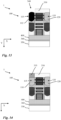
- a transistor structure 100 according to embodiments, which may be formed by performing frontside processing.
- the transistor structure 100 forms part of a complementary field effect transistor (CFET) structure 10 which may be formed performing frontside processing.
- the CFET structure 10 forms part of the device structure 1 depicted in Fig. 1 .
- the device structure 1 includes all elements and structures depicted in Fig. 1 .
- a CFET typically comprises a PMOS transistor structure 100 and a NMOS transistor structure 200 vertically stacked on top of each other.
- the device structure or structure 1 of Fig. 1 further comprises structures 400 which are formed during middle-of-line (MOL) and back-end-of-line (BEOL) processes. Those structures 400 will also be illustrated throughout the drawings for illustrative completeness and clarity. However, the transistor structure 200 and the structures 400 will not be described in greater detail.
- MOL middle-of-line
- BEOL back-end-of-line
- non-stacked semiconductor structures 100 such as non-stacked nanosheet-FET devices and fin-FET devices.
- the substrate 300 may be a conventional semiconductor substrate suitable for complementary FETs.
- the substrate 300 may be a single-layered semiconductor substrate, for instance formed by a bulk substrate such as a Si substrate, a germanium (Ge) substrate or a silicon-germanium (SiGe) substrate.
- a multi-layered / composite substrate is however also possible, such as an epitaxially grown semiconductor layer on a bulk substrate, or a semiconductor-on-insulator (SOI) substrate, such as a Si-on-insulator substrate, a Ge-on-insulator substrate, or a SiGe-on-insulator substrate.
- SOI semiconductor-on-insulator
- the transistor structure 100 comprises a first S/D body 110 and a second S/D body 120.
- the first S/D body 110 is located in a first S/D region 115.
- the second S/D body 120 is located in a second S/D region 125.
- the first S/D body 110 and a second S/D body 120 may be formed by epitaxially growing the first S/D body 110 and a second S/D body 120.
- the first S/D body 110 and the second S/D body 120 may for instance be formed by epitaxially growing doped Si, Si-C, SiGe, Ge, Ge-Sn, or SiGe-Sn.
- a channel structure 130 is provided between the first S/D body 110 and the second S/D body 120.
- the depicted channel structure 130 comprises channel layers 132 in form of nano-sheet channel layers 132.
- the nano-sheet channel layers 132 depicted in Fig. 1 extends between the first S/D body 110 and the second S/D body 120. In Fig. 1 , only two nano-sheet channel layers 132 are illustrated for illustrational clarity although the channel structure 130 may comprise any number of channel layers 132.
- the channel layers 132 of the channel structure 130 may comprise a high mobility channel material.
- the channel layers 132 may according to embodiments comprise one or more layers 132 of a Ge-comprising channel material.
- the channel layers 132 may according to embodiments comprise one or more layers 132 of Ge as the channel material.
- the channel layers 132 may according to embodiments comprise one or more layers 132 of a SiGe-comprising channel material.
- the Ge concentration may be equal to or above 70% in order to provide a high mobility channel.
- the present disclosure is also applicable for lower Ge concentrations.
- the present disclosure is also applicable for Si-based channel materials.
- the channel region 130 may comprise a single channel in channel region. Further, the channel region 130 may comprise channels in form of nanowires.
- the depicted channel layers 132 of the channel structure 130 are surrounded by a gate stack 140.
- the gate stack 140 is schematically drawn and may as is known in the art comprise a gate dielectric and one or more gate metal layers. The gate stack will not be described in greater detail here. However, it is to be understood that any type of suitable gate stack 140 may be used. Further, according to embodiments the gate stack 140 may be provided directly on top of the channel region 130 e.g. in case of a single channel in the channel region 130.
- the depicted gate stack 140 is separated from the first S/D body 110 and the second S/D body 120 by an inner spacer 150.
- the inner spacer 150 which is known per se and may be formed according to known techniques.
- the first S/D body 110 and the second S/D body 120 have a first doping concentration.
- the first doping concentration may lie in the range of 1 ⁇ 10 17 - 1 ⁇ 10 22 dopants per cubic centimeter.
- the first S/D body 110 and the second S/D body 120 may be doped with P, As, Sb, Ga, or B.
- the first S/D body 110 and the second S/D body 120 may typically be formed simultaneously using the same processing steps to arrive at the first doping concentration.
- Fig. 2 illustrates how the complete structure 1 of Fig. 1 has been bonded to a carrier substrate or wafer 350 by a bonding layer 360.
- the carrier substrate may be a silicon wafer.
- the bonding layer may be an oxide or nitride bonding layer, or any other conventional type of bonding layer suitable for CMOS-processing.
- the complete structure has been flipped upside down such that the substrate 300 which was depicted at the bottom in Fig. 1 is now located at the top as clearly illustrated in Fig. 2 .
- the flipping of the complete structure 1 is also indicated by the altered direction of the Y-axis in Fig. 2 in relation to Fig. 1 .
- the complete structure 1 is prepared for being subjected to backside processing.
- the complete structure 1 of Figs. 1 and 2 may be subjected to backside processing subsequent to being subjected to frontside processing. More specifically, it will be described how the first S/D body 110 of the transistor structure 100 may be exposed from a backside 300b of the substrate 300 and how the first S/D body 110 may be processed to form a replacement S/D body 112 in the first S/D region 115, where the replacement S/D body 112 has a second doping concentration which is different from the first doping concentration.
- the replacement S/D body 112 which has a doping concentration different from the one of the first S/D body 110, is formed in the first S/D region 115 via backside processing of the transistor structure 100.
- the first S/D body 110 may define a source body 110 and the second S/D body 120 may define a drain body, wherein a replacement source body 112 with a doping concentration different from (e.g., higher) than the original source body 110 may be formed.
- first S/D body 110 may also define a drain body 110 and the second S/D body 120 may define a source body, wherein a replacement drain body 112 with a doping concentration different from (e.g., lower) than the original drain body 120 may be formed.
- a first approach for forming a replacement S/D body 112 will be disclosed with refence to Fig. 1-5 .
- a second approach for forming a replacement S/D body 112 will be disclosed with refence to Fig. 6-8
- a third approach for forming a replacement S/D body 112 will be disclosed with refence to Fig. 10-13 .
- Fig. 3 illustrates how the substrate 300 has been subjected to thinning from the backside 300b thereof such that only a limited portion of the substrate 300 remains underneath the transistor structure 100.
- the substrate 300 may be thinned by grinding or chemical mechanical polishing (CMP), and/or etch back (e.g., anisotropic dry etching, wet etching, a gas chemical etch process like siconi or a certas type of process).
- CMP chemical mechanical polishing
- an opening 310 has been formed in the substrate 300.
- the opening 310 exposes the first S/D body 110 from the backside 300b of the substrate 300 as depicted in Fig. 4 .
- the opening 310 has been formed in the substrate 300 underneath the first S/D body 110 as illustrated in Fig. 4 .
- the opening 310 may be formed in the substrate by conventional lithographic and etching processes. For instance, a photomask may be formed on the backside of the thinned substrate 300 and used as an etch mask for forming the opening 310 in the substrate 300.
- the first S/D body 110 may be processed from the opening 310 to form, the replacement S/D body 112 (see e.g. Fig. 5 ) in the first S/D region 115.
- the processing of the first S/D body 110 may, as indicated above, aim at forming the replacement S/D body 112 having a second doping concentration different from the first doping concentration. In this way, an asymmetric transistor structure, i.e. a non-uniform transistor structure with asymmetric source drain doping may be formed.
- Fig. 5 illustrates the structure 1 after the first S/D body 110 has been processed to form, in the first S/D region 115, the replacement S/D body 112. More specifically, the replacement S/D body 112 of Fig. 5 has been formed by increasing the doping concentration in the first S/D body 110. In other words, the material of the first S/D body 110 has been modified by increasing the doping concentration in the material of the first S/D body.
- the doping concentration of the first S/D body 110 may be increased by implanting dopants into the first S/D body 110, and/or by diffusing dopants into the first S/D body 100 as generally indicated by the arrows in Fig. 5 .
- the doping concentration of the first S/D body 110 may be increased by implanting or diffusing P, As, Sb, Ga or B into the first S/D body 100.
- the doping concentration of the replacement S/D body 112 of Fig. 5 may lie in a part of the range of 1 ⁇ 10 17 - 1 ⁇ 10 22 dopants per cubic centimeter above the doping concentration of the first S/D body 110.
- Fig. 6 illustrates the structure 1 of Fig. 4 after the structure 1 has been subjected to further processing steps prior to processing the first S/D body 110 to form the replacement S/D body 112.
- an insulating liner 320 covering the substrate and the exposed first S/D body 115 has been formed.
- the insulating liner 320 may be formed by conformally depositing a dielectric material such as, an insulating oxide or nitride, over the backside 300b of the substrate 300 and over the interior surfaces of the opening 310 including the exposed portions of the exposed first S/D body 110.
- the insulating liner 320 may include silicon dioxide or silicon nitride.
- the insulating liner 320 has been opened in (i.e., via or from) the opening 310 in the substrate 300, thereby forming an opening 311 in the insulating liner 320.
- the first S/D body 110 has been exposed via the openings 310 and 311.
- Part of the insulating liner 320 may be removed by a conventional pattering and etching process. For instance, a patterned resist may be used as an etch mask for opening the insulating liner 320 in the opening 310 of the substrate 300.
- the first S/D body 110 has been substantially completely removed to form a S/D body cavity 117 the first S/D region 115.
- at least a portion of the first S/D body 110, or at least a major portion of the first S/D body 110 may be removed, to form the S/D body cavity 117 in the first S/D region 115, as indicated by the hatched line in the S/D body cavity 117 of the first S/D region 115.
- the shape of the hatched line merely is schematic.
- the S/D body cavity 117 may instead be formed in a center portion of the first S/D body 110 such that portions of the first S/D body 110 remain adjacent the channel layers 132 and inner spacers 150.
- Fig. 8 illustrates the structure 1 of Fig. 7 .
- the structure of Fig 7 has been subjected to further processing steps.
- doped S/D material has been epitaxially grown in the first S/D region 115.
- doped S/D material has been epitaxially grown via the opening in the insulating liner 320. That is, doped S/D material has been epitaxially grown in the S/D body cavity 117.
- the first S/D body has been processed from the opening in the insulating liner 320 to form a replacement S/D body 112 having a second doping concentration which is different from the first doping concentration.
- the S/D material may be doped with P, As, Sb, Ga or B.
- the doped S/D material may be grown by chemical vapor deposition (CVD) or atomic layer deposition (ALD) processes.
- the doping concentration of the replacement S/D body 112 of Fig. 8 may lie in the range of 1 ⁇ 10 17 - 1 ⁇ 10 22 dopants per cubic centimeter.
- the doped S/D material may comprise the same material or materials as the first S/D body but with a different doping concentration.
- the formed replacement S/D body 112 will in practice in part be formed of the initial first S/D body 110 and in part be formed of the epitaxially grown doped S/D material. Further, the formed replacement S/D body 112 will have a doping concentration which is different from that of the first S/D body by the doped S/D material having a doping concentration being different from that of the first S/D body.
- an S/D contact 114 has been formed on the replacement S/D body 112.
- the S/D contact 114 has been formed from the backside 300b of the substrate 300.
- the S/D contact 114 may be formed using conventional methods.
- FIG. 10 illustrates the structure 1 of Fig. 2 .
- the structure of Fig 2 has been subjected to further processing steps.
- the substrate 300 has been removed underneath the transistor structure 100 to expose the first S/D body 110 and the second S/D body 120.
- the substrate 300 may be removed underneath the transistor structure 100 using conventional processes including grinding or CMP and/or etching, such as dry etching, wet etching, a gas chemical etch process like siconi or a certas type of process.
- a bottom isolation layer 330 covering the first S/D body 110 and the second S/D body 120 has been formed.
- the bottom isolation layer 330 may be formed by e.g., depositing or growing silicon dioxide or silicon nitride such that the bottom isolation layer 330 covers the first S/D body 110 and the second S/D body as illustrated in Fig. 11 .
- the bottom isolation layer 330 may for instance be formed by CVD, ALD or physical vapor deposition (PVD).
- an opening 340 has been formed in the bottom isolation layer 330 to expose the first S/D body 110.
- the opening 340 in the bottom isolation layer 330 may formed by a conventional pattering and etching process. For instance, a patterned resist may be used as an etch mask for forming the opening 340.
- the first S/D body 110 has been substantially completely removed.
- the removal of the first S/D body may result in that a S/D body cavity 117 is formed.
- the formation of the S/D body cavity 117 has been described above in conjunction with Fig. 7 to which reference is made.
- at least a portion of the first S/D body 110, or at least a major portion of the first S/D body 110 may be removed, to form the S/D body cavity 117 in the first S/D region 115.
- the first S/D body 110 has been processed from the opening 340 in the bottom isolation layer 330. More specifically, the first S/D body 110 may be processed as have been described above in conjunction to Fig. 8 to form the replacement S/D body 112 having a second doping concentration which is different from the first doping concentration. Hence, reference is made to the above. Further, an S/D contact 114 may be formed on the replacement S/D body 112 as has been described above in conjunction with Fig. 9 .
- Fig. 14 illustrates a structure 1 highly similar to the structure 1 of Fig. 11 .
- a dummy contact plug 335 is provided underneath the first S/D body 110 as illustrated in Fig. 14 .
- the dummy contact plug 335 of Fig. 14 has been formed during front side processing taking place prior to the backside processing.
- an opening 340 corresponding to the opening 340 of Fig. 11 may be formed by removing the dummy contact plug 335.
- the opening 340 in the bottom isolation layer 330 may be formed by removing the dummy contact plug 335 provided underneath the first S/D body 110.
- the dummy contact plug 335 may be formed during front side processing prior to forming the transistor structure 100, by e.g. forming a recess in the substrate 300, with a well-controlled overlay with respect to the S/D region 115, and forming the dummy contact plug 335 in the recess.
- the dummy contact plug 335 may be formed by a dummy material such as amorphous silicon, an epitaxial semiconductor material (e.g., Ge, Si or SiGe), a dielectric material, or more generally any suitable dummy material which may be removed selectively to the bottom isolation layer 330, and which is compatible (e.g., in terms of thermal budget) with the preceding steps of the frontside and backside-processing.
- the opening 340 may be formed in a self-aligned manner with respect to the first S/D body 110.
- an opening 310 may be formed in the substrate 300 by removing the dummy contact plug 335.
- an opening 310 may be formed in the substrate as illustrated in Fig. 4 .
- the formation of such opening 310 may comprise thinning the substrate 300 to expose the dummy contact plug 335 provided underneath the first S/D body 110, and removing the dummy contact plug 335 to expose the first S/D body 110.
- the structure 1 may be processed as have been described above in conjunction with Figs. 5 , 8 or 13 to form the replacement S/D body 112 having a second doping concentration different from the first doping concentration. Further, an S/D contact 114 may be formed on the replacement S/D body 112 as have been described above in conjunction with Fig. 9 .
- Fig. 15 illustrates a structure 1 highly similar to the structure 1 of Fig. 11 .
- the first S/D body 110 comprises a semiconductor liner 111.
- the semiconductor liner 111 is provided at least at an interface between the first S/D body 11 and the channel structure 130.
- the semiconductor liner 111 may be for instance also be provided underneath the first S/D body as illustrated in Fig. 15 .
- the semiconductor liner 111 may be formed of a material different from a material of the first S/D body 110.
- the semiconductor liner 111 may for instance be formed of silicon or silicon germanium having a low germanium content than the first S/D body 110. In this regard, when the semiconductor liner 111 is formed of silicon germanium the germanium content may typically be lower than a germanium content of the first S/D body 110 in case also the first S/D body is formed of silicon germanium.
- the first S/D body 110 may be etched selectively with respect to the semiconductor liner 111.
- at least a portion or at least a major portion of the first S/D body 110 may be removed using an etching process etching the material of the first S/D body selective to the material of the semiconductor liner 111.
- a source body cavity 117 corresponding to the source body cavity of Fig. 12 may be formed.
- the semiconductor liner 111 formed of a material different from a material of the first S/D body 110, the removal or partial removal of the first S/D body may be performed with a reduced risk of damaging the channel structure 130.
- the semiconductor liner 111 may be formed by a silicon germanium material with a germanium concentration which differs from the material of the first S/D body by 10% or more (e.g., being at least 10% greater or smaller).
- the replacement S/D body may comprise more than one material or material composition.
- the replacement S/D body may comprise two or more layers having different material compositions.
- the replacement S/D body may comprise two or more layers of SiGe with different Ge concentrations.
- a dummy contact plug 335 may be used in coordination with a first S/D body comprising a semiconductor liner 111.
- a dummy contact plug 335 may be used in coordination with an insulating layer 320.
- a S/D contact 114 may be formed on any replacement S/D body 112 described above.
- additional backside processing steps may be applied to the structure 10.
- the method may proceed with forming a backside interconnect structure for routing signals or power to the transistor structure 100, e.g. via the S/D contact 114, and to any further devices (e.g., CFETs) of the device structure 1.
- a backside interconnect structure may be formed using conventional techniques used in the BEOL for forming frontside interconnect structures, such as damascene processing. The specific layout and details of the backside interconnect structure are beyond the scope of the present methods and will hence not be further discussed herein.
Landscapes
- Thin Film Transistor (AREA)
Abstract
Description
- The present invention generally relates to a method for forming a semiconductor device.
- The use of high mobility channel materials has long attracted great interest in the semiconductor industry since high mobility channel materials have a bulk mobility exceeding that of Si which is the most commonly used channel material. For instance, Ge has a bulk mobility which is 4.4 times higher for holes and 2.4 times higher for electrons as compared to Si. Such high bulk mobility generally results in a high drivability with high on-state currents, ION, of for instance Ge FETs. However, such high mobility channel material devices typically suffer from significantly higher band-to-band-tunneling, BTBT e.g. owing from their small bandgap, and thus higher off-state leakage currents, IOFF. Hence, there is a need to be able to manufacture high mobility channel material devices which exhibit lower off-state leakage currents while still taking advantage of the high drivability, and thus high on-state currents.
- In light of the above, it is an object of the present invention to provide a method for forming a semiconductor device which mitigates at least some of the issues associated with high mobility channel material devices.
- Hence, it is an object to provide a method for forming a semiconductor device which enables formation of a high mobility channel material semiconductor device with a reduced off-state leakage current.
- Another object is to provide a method for forming a semiconductor device which enables formation of a high mobility channel material semiconductor device which has a high drivability, and hence a high on-state current, with a reduced off-state leakage current.
- Another object is to provide a method for forming a semiconductor device which enables formation of a high mobility channel material semiconductor device with a reduced contact resistance.
- Another object is to provide a method for forming a semiconductor device which requires fewer process steps.
- Another object is to provide a method for forming a semiconductor device which is less complex.
- Another object is to provide a method for forming a semiconductor device which is more cost-effective.
- These and other objects may be achieved by a method for forming a semiconductor device in accordance with the independent claim. Embodiments of the present invention are defined in the dependent claims.
- Hence, according to an aspect of the present invention, there is provided a method for forming a semiconductor device, comprising: performing frontside processing comprising forming a transistor structure on a frontside of a substrate, the transistor structure comprising a first source/drain body and a second source/drain body located in a first and a second source/drain region, respectively, and a channel structure between the first source/drain body and the second source/drain body, wherein the first source/drain body and the second source/drain body have a first doping concentration; subsequent to the frontside processing, performing backside processing comprising: exposing the first source/drain body from a backside of the substrate; and processing the first source/drain body to form, in the first source/drain region, a replacement source/drain body having a second doping concentration different from the first doping concentration.
- Thus, the present invention is based on the insight that by processing the first source/drain body to form a replacement source/drain body which has a different doping concentration than the second source/drain body, an asymmetric semiconductor device, i.e. a device with an asymmetric doping of the source/drain bodies, may be formed. In particular, an asymmetric high mobility channel material semiconductor device or high mobility device may be formed.
- In this regard, in order to provide a high mobility device which offers high drivability and low off-state currents the device will typically have a high source doping, which allows for high on-state currents, while at the same time have low drain doping, which allows for low off-state leakage currents.
- Further, the present method may allow for forming an asymmetric high mobility channel material semiconductor device or high mobility device while using fewer process steps as compared to traditional methods. More specifically, by processing the first source/drain body during the backside processing, which anyhow may involve accessing the first source/drain body for contacting with a backside power delivery network, the asymmetric doping may be provided without adding additional process steps during the frontside processing. Accordingly, the present method may be especially beneficial in fabrication of a semiconductor device comprising a backside power delivery network.
- Furthermore, the present method may allow for forming an asymmetric high mobility channel material semiconductor device or high mobility device in a less complex way at a reduced cost.
- The first source/drain body and the second source/drain body may be a source body and a drain body, respectively. Alternatively, the first source/drain body and the second source/drain body may be a drain body and a source body, respectively. This applies correspondingly to the first and second source/drain regions.
- In practice, in a case where the first source/drain body and the first source/drain region is a source body and a source region, respectively, the present method enables forming an asymmetric device by increasing the doping concentration in the source region by forming the replacement source body with a higher doping concentration as compared to the concentration of the drain body.
- Conversely, in practice, in a case where the first source/drain body and the first source/drain region is a drain body and a drain region, respectively, the present method enables forming an asymmetric device by decreasing the doping concentration in the drain region by forming the replacement drain body with a lower doping concentration as compared to the concentration of the source body.
- Consequently, more generally, the present method enables fabrication of an asymmetric device by increasing or decreasing the doping concentration in the first source/drain region while not affecting, or in principle not affecting, the doping concentration in the second source/drain region.
- More specifically, the difference in doping concentrations between the replacement source/drain body and the second source/drain body is by the present method achieved by processing the first source/drain body to form, in the first source/drain region, a replacement source/drain body having a second doping concentration different from the first doping concentration. Thereby, an asymmetric transistor structure, i.e. a non-uniform transistor structure with asymmetric source drain doping is formed.
- Thus, by forming the first source/drain body and the second source/drain body with a first doping concentration during frontside processing, and subsequently during backside processing, processing the first source/drain body to form a replacement source body having a second doping concentration different from the first doping concentration, the asymmetry of the formed semiconductor device may be tailored by tailoring the first and the second doping concentrations.
- By "replacement source/drain body" is here meant a source/drain body having properties different from those of the first source/drain body which is formed during the frontside processing. In particular, the replacement source/drain body may have a higher doping concentration as compared to the first source/drain body formed during the frontside processing, or, the replacement source/drain body may have a lower doping concentration as compared to the first source/drain body formed during the frontside processing.
- The replacement source/drain body may comprise material from the first source/drain body formed during the frontside processing. The replacement source /drain body may comprise other material than the material of the first source/drain body formed during the frontside processing. Thus, the replacement source/drain body may for example be formed by altering the first source/drain body formed during the frontside processing. The replacement source/drain body may for example be formed by altering a portion of the first source/drain body formed during the frontside processing. The replacement source/drain body may for example be formed partially replacing the first source/drain body formed during the frontside processing. The replacement source/drain body may for example be formed replacing the first source/drain body formed during the frontside processing. The replacement source/drain body may for example be formed by adding material to the first source/drain body formed during the frontside processing. The replacement source/drain body may for example be formed by a combination of the above techniques.
- According to some embodiments, processing the first source/drain body may comprise epitaxially growing doped source/drain material in the first source/drain region, which is advantageous in that the replacement source/drain body may be formed by epitaxial material with a higher or lower doping concentration as compared to the first source/drain body. The replacement source/drain body may be formed with a higher doping concentration as compared to the first source/drain body by epitaxially growing doped source/drain material having a doping concentration higher than the first doping concentration. In this way, the overall or average doping concentration of the replacement source/drain body may be increased relative to the first and second source/drain bodies. Alternatively, the replacement source/drain body may be formed with a lower doping concentration as compared to the first source/drain body by epitaxially growing doped source/drain material having a doping concentration lower than the first doping concentration. In this way, the overall or average doping concentration of the replacement source body may be decreased relative to the first and second source/drain bodies.
- According to some embodiments, the doped source/drain material may be grown on an exposed surface of the first source/drain body, which is advantageous in that the first source/drain body may be at least partly preserved in the first source/drain region. This may facilitate the processing since less material of the first source/drain body needs to be removed.
- According to some embodiments, processing the first source/drain body may further comprise; removing at least a portion the first source/drain body, or at least a major portion of the first source/drain body, to form a source/drain body cavity in the first source/drain region, wherein the doped source/drain material subsequently is epitaxially grown in the source/drain body cavity. By removing at least a portion of the first source/drain body a source/drain body cavity corresponding to a least a portion of the first source/drain body may be formed in the first source/drain region. By subsequently epitaxially growing the doped source/drain material in the source/drain body cavity the resulting replacement source/drain body may be formed with the second doping concentration. The effective doping concentration of the composite replacement source/drain body (formed by the remaining portion of the first source/drain body and the epitaxial source/drain material) may hence be controlled by varying the amount of material removed from the first source/drain body. Similarly, by removing at least a major portion of the first source/drain body a source/drain body cavity corresponding to a least a major portion of the first source/drain body may be formed in the first source/drain region. By subsequently epitaxially growing the doped source/drain material in the source/drain body cavity the resulting replacement source/drain body may be formed with the second doping concentration. The second doping concentration may hence be provided in a greater part of the replacement source/drain body.
- According to some embodiments, the first source/drain body may comprise a semiconductor liner provided at least at an interface between the first source/drain body and the channel structure, wherein the semiconductor liner is formed of a material different from a material of the first source/drain body, which is advantageous in that the liner may protect the channel structure during the backside processing. For instance, the liner may protect the channel structure while forming the source/drain body cavity. Furthermore, the liner may protect the channel structure during the frontside processing.
- According to some embodiments, the at least a portion or the at least a major portion of the first source/drain body may be removed using an etching process etching the material of the first source/drain body selective to the material of the semiconductor liner, which is advantageous in that the extension of the source/drain body cavity may be controlled by the presence of the liner. Further, the liner may prevent or counteract that the channel structure is affected by the etchants used for forming the source/drain body cavity.
- According to some embodiments, exposing the first source/drain body may comprise thinning the substrate from the backside.
- According to some embodiments, exposing the first source/drain body may comprise forming an opening in the substrate underneath the first source/drain body to expose the first source/drain body, wherein the first source/drain body is processed from the opening in the substrate.
- According to some embodiments, forming the opening in the substrate may comprise thinning the substrate to expose a dummy contact plug provided underneath the first source/drain body, and removing the dummy contact plug to expose the first source/drain body.
- According to some embodiments, the method may further comprise: subsequent to forming the opening in the substrate, forming an insulating liner covering the substrate and the exposed first source/drain body; and opening the insulating liner in the opening in the substrate to expose the first source/drain body, wherein the first source/drain body is processed from the opening in the insulating liner, which is advantageous in that the insulating liner may protect the substrate during the backside processing.
- According to some embodiments, the doped source/drain material may be epitaxially grown via the opening in the insulating liner, which is advantageous in that the insulating liner may inhibit the doped source/drain material from growing at the substrate while being epitaxially grown via the opening in the insulating liner. The insulating liner may thus be used as an epitaxy mask inhibiting deposition of source/drain material in regions other than the first source/drain region.
- According to some embodiments, the at least a portion or the at least a major portion of the first source/drain body may be removed by etching from the opening in the insulating liner, which is advantageous in that the insulating liner may prevent or counteract that the substrate is affected by the etching. The insulating liner may thus be used as an etch mask when etching the first source/drain body.
- According to some embodiments, exposing the first source/drain body may comprise: removing the substrate underneath the transistor structure to expose the first source/drain body and the second source/drain body; forming a bottom isolation layer covering the first source/drain body and the second source/drain body; and forming an opening in the bottom isolation layer to expose the first source/drain body; wherein the first source/drain body is processed from the opening in the bottom isolation layer, which is advantageous in that the bottom isolation layer may protect the transistor structure while processing the first source/drain body from the opening in the bottom isolation layer.
- According to some embodiments, the opening in the bottom isolation layer may formed by removing a dummy contact plug provided underneath the first source/drain body, which is advantageous in that the opening in the bottom isolation layer may be formed in a self-aligned manner.
- According to some embodiments, processing the first source/drain body may comprise increasing the doping concentration in the first source/drain body, and wherein increasing the doping concentration comprises: implanting dopants into the first source/drain body, and/or diffusing dopants into the first source/drain body. The doping concentration in the replacement source/drain body may hence be increased by selectively introducing dopants in the first source/drain body (but not the second source/drain body).
- According to some embodiments, the method may further comprise: forming a source/drain contact on the replacement source/drain body, which is advantageous in that a reduced contact resistance may be achieved between the replacement source/drain body and the source/drain contact as compared to if the source/drain contact were to be formed on the first source/drain body.
- According to some embodiments, the frontside processing may further comprise forming a source/drain contact on the second source/drain body.
- According to some embodiments, the frontside processing may further comprise forming a gate stack on the channel structure.
- According to some embodiments, the channel structure may comprise one or more layers of a Ge-comprising channel material.
- According to some embodiments, the channel structure may comprise one or more layers of a SiGe-comprising channel material.
- This and other aspects of the present invention will now be described in more detail, with reference to the appended drawings showing embodiments of the present invention.
-
Figs. 1-4 schematically shows a device structure at different stages of a method for forming a semiconductor structure. -
Fig. 5 schematically shows how a replacement source/drain body may be formed according to embodiments. -
Figs. 6-8 schematically shows a device structure at different stages of a method for forming a semiconductor structure. -
Fig. 9 schematically shows how a source/drain contact may be formed according to embodiments. -
Figs. 10-13 schematically shows a device structure at different stages of a method for forming a semiconductor structure. -
Fig. 14 schematically shows a device structure comprising a dummy contact plug. -
Fig. 15 schematically shows a device structure in which the first source/drain body comprises a semiconductor liner. - Hereafter follows a detailed description of various method embodiments for forming a semiconductor device. More specifically, the methods comprise, subsequent to the frontside processing, performing backside processing including processing a first source/drain (S/D) body to form, in a first S/D region, a replacement S/D body having a doping concentration different from the doping concentration of the first S/D body. The methods will be described with reference to the drawings.
- The drawings are only schematic and the relative dimensions of some structures and layers may be exaggerated and not drawn to scale. Rather the dimensions may be adapted for illustrational clarity and to facilitate understanding. When present in the figures, the indicated axes X and Y consistently refer to a horizontal or lateral direction, and a vertical direction, respectively. As used herein, the terms "horizontal" and "lateral" refer to directions parallel to (a main surface of) a substrate on/from which the semiconductor device being formed. The term "vertical" refers to a direction parallel to a normal direction of (a main surface of) the substrate on/from which the semiconductor device being formed, i.e., transverse to the substrate. Further, the (positive) vertical direction refers to a direction which points out of what typically is regarded as a frontside of the substrate.
- Initially it will be briefly described with reference to
Fig. 1 , atransistor structure 100 according to embodiments, which may be formed by performing frontside processing. InFig. 1 , thetransistor structure 100 forms part of a complementary field effect transistor (CFET)structure 10 which may be formed performing frontside processing. TheCFET structure 10 forms part of thedevice structure 1 depicted inFig. 1 . Hence, thedevice structure 1 includes all elements and structures depicted inFig. 1 . In the following, thedevice structure 1 will be described at different stages of method embodiments while referring to the drawings. As is known in the art, a CFET typically comprises aPMOS transistor structure 100 and aNMOS transistor structure 200 vertically stacked on top of each other. In the following description, thetransistor structure 100 located closest to thesubstrate 300 will be described although thetransistor structure 200 will also be illustrated throughout the drawings for illustrative completeness and clarity. The device structure orstructure 1 ofFig. 1 further comprisesstructures 400 which are formed during middle-of-line (MOL) and back-end-of-line (BEOL) processes. Thosestructures 400 will also be illustrated throughout the drawings for illustrative completeness and clarity. However, thetransistor structure 200 and thestructures 400 will not be described in greater detail. - Further, is it to be understood that the present disclosure is equally applicable to
non-stacked semiconductor structures 100, such as non-stacked nanosheet-FET devices and fin-FET devices. - As depicted in
Fig. 1 , thetransistor structure 100 has been formed on a frontside 300a of asubstrate 300. Thesubstrate 300 may be a conventional semiconductor substrate suitable for complementary FETs. Thesubstrate 300 may be a single-layered semiconductor substrate, for instance formed by a bulk substrate such as a Si substrate, a germanium (Ge) substrate or a silicon-germanium (SiGe) substrate. A multi-layered / composite substrate is however also possible, such as an epitaxially grown semiconductor layer on a bulk substrate, or a semiconductor-on-insulator (SOI) substrate, such as a Si-on-insulator substrate, a Ge-on-insulator substrate, or a SiGe-on-insulator substrate. - The
transistor structure 100 comprises a first S/D body 110 and a second S/D body 120. The first S/D body 110 is located in a first S/D region 115. The second S/D body 120 is located in a second S/D region 125. - The first S/
D body 110 and a second S/D body 120 may be formed by epitaxially growing the first S/D body 110 and a second S/D body 120. The first S/D body 110 and the second S/D body 120 may for instance be formed by epitaxially growing doped Si, Si-C, SiGe, Ge, Ge-Sn, or SiGe-Sn. - A
channel structure 130 is provided between the first S/D body 110 and the second S/D body 120. The depictedchannel structure 130 comprises channel layers 132 in form of nano-sheet channel layers 132. The nano-sheet channel layers 132 depicted inFig. 1 extends between the first S/D body 110 and the second S/D body 120. InFig. 1 , only two nano-sheet channel layers 132 are illustrated for illustrational clarity although thechannel structure 130 may comprise any number of channel layers 132. The channel layers 132 of thechannel structure 130 may comprise a high mobility channel material. The channel layers 132 may according to embodiments comprise one ormore layers 132 of a Ge-comprising channel material. The channel layers 132 may according to embodiments comprise one ormore layers 132 of Ge as the channel material. The channel layers 132 may according to embodiments comprise one ormore layers 132 of a SiGe-comprising channel material. In case the channel layers 132 comprise a SiGe-comprising channel material, the Ge concentration may be equal to or above 70% in order to provide a high mobility channel. However, the present disclosure is also applicable for lower Ge concentrations. Similarly, the present disclosure is also applicable for Si-based channel materials. - Further, according to embodiments the
channel region 130 may comprise a single channel in channel region. Further, thechannel region 130 may comprise channels in form of nanowires. - The depicted
channel layers 132 of thechannel structure 130 are surrounded by agate stack 140. Thegate stack 140 is schematically drawn and may as is known in the art comprise a gate dielectric and one or more gate metal layers. The gate stack will not be described in greater detail here. However, it is to be understood that any type ofsuitable gate stack 140 may be used. Further, according to embodiments thegate stack 140 may be provided directly on top of thechannel region 130 e.g. in case of a single channel in thechannel region 130. - Further, the depicted
gate stack 140 is separated from the first S/D body 110 and the second S/D body 120 by aninner spacer 150. Theinner spacer 150 which is known per se and may be formed according to known techniques. - The first S/
D body 110 and the second S/D body 120 have a first doping concentration. The first doping concentration may lie in the range of 1·1017 - 1·1022 dopants per cubic centimeter. The first S/D body 110 and the second S/D body 120 may be doped with P, As, Sb, Ga, or B. The first S/D body 110 and the second S/D body 120 may typically be formed simultaneously using the same processing steps to arrive at the first doping concentration. - Now also turning to
Fig. 2. Fig. 2 illustrates how thecomplete structure 1 ofFig. 1 has been bonded to a carrier substrate orwafer 350 by abonding layer 360. The carrier substrate may be a silicon wafer. The bonding layer may be an oxide or nitride bonding layer, or any other conventional type of bonding layer suitable for CMOS-processing. Further, the complete structure has been flipped upside down such that thesubstrate 300 which was depicted at the bottom inFig. 1 is now located at the top as clearly illustrated inFig. 2 . The flipping of thecomplete structure 1 is also indicated by the altered direction of the Y-axis inFig. 2 in relation toFig. 1 . By bonding thecomplete structure 1 ofFig. 1 to thecarrier substrate 350 and flipping thecomplete structure 1, thecomplete structure 1 is prepared for being subjected to backside processing. - In the following it will be described how the
complete structure 1 ofFigs. 1 and 2 may be subjected to backside processing subsequent to being subjected to frontside processing. More specifically, it will be described how the first S/D body 110 of thetransistor structure 100 may be exposed from abackside 300b of thesubstrate 300 and how the first S/D body 110 may be processed to form a replacement S/D body 112 in the first S/D region 115, where the replacement S/D body 112 has a second doping concentration which is different from the first doping concentration. In other words, it will in the following be described how the replacement S/D body 112, which has a doping concentration different from the one of the first S/D body 110, is formed in the first S/D region 115 via backside processing of thetransistor structure 100. As previously discussed, the first S/D body 110 may define asource body 110 and the second S/D body 120 may define a drain body, wherein areplacement source body 112 with a doping concentration different from (e.g., higher) than theoriginal source body 110 may be formed. However, the first S/D body 110 may also define adrain body 110 and the second S/D body 120 may define a source body, wherein areplacement drain body 112 with a doping concentration different from (e.g., lower) than theoriginal drain body 120 may be formed. - A first approach for forming a replacement S/
D body 112 will be disclosed with refence toFig. 1-5 . Followingly, a second approach for forming a replacement S/D body 112 will be disclosed with refence toFig. 6-8 Thereafter, a third approach for forming a replacement S/D body 112 will be disclosed with refence toFig. 10-13 . - Now also turning to
Fig. 3. Fig. 3 illustrates how thesubstrate 300 has been subjected to thinning from thebackside 300b thereof such that only a limited portion of thesubstrate 300 remains underneath thetransistor structure 100. In practice, thesubstrate 300 may be thinned by grinding or chemical mechanical polishing (CMP), and/or etch back (e.g., anisotropic dry etching, wet etching, a gas chemical etch process like siconi or a certas type of process). - Now also turning to
Fig. 4 , there is shown that anopening 310 has been formed in thesubstrate 300. Theopening 310 exposes the first S/D body 110 from thebackside 300b of thesubstrate 300 as depicted inFig. 4 . Thus, theopening 310 has been formed in thesubstrate 300 underneath the first S/D body 110 as illustrated inFig. 4 . Theopening 310 may be formed in the substrate by conventional lithographic and etching processes. For instance, a photomask may be formed on the backside of the thinnedsubstrate 300 and used as an etch mask for forming theopening 310 in thesubstrate 300. - The first S/
D body 110 may be processed from theopening 310 to form, the replacement S/D body 112 (see e.g.Fig. 5 ) in the first S/D region 115. The processing of the first S/D body 110 may, as indicated above, aim at forming the replacement S/D body 112 having a second doping concentration different from the first doping concentration. In this way, an asymmetric transistor structure, i.e. a non-uniform transistor structure with asymmetric source drain doping may be formed. -
Fig. 5 illustrates thestructure 1 after the first S/D body 110 has been processed to form, in the first S/D region 115, the replacement S/D body 112. More specifically, the replacement S/D body 112 ofFig. 5 has been formed by increasing the doping concentration in the first S/D body 110. In other words, the material of the first S/D body 110 has been modified by increasing the doping concentration in the material of the first S/D body. The doping concentration of the first S/D body 110 may be increased by implanting dopants into the first S/D body 110, and/or by diffusing dopants into the first S/D body 100 as generally indicated by the arrows inFig. 5 . The doping concentration of the first S/D body 110 may be increased by implanting or diffusing P, As, Sb, Ga or B into the first S/D body 100. The doping concentration of the replacement S/D body 112 ofFig. 5 may lie in a part of the range of 1·1017 - 1·1022 dopants per cubic centimeter above the doping concentration of the first S/D body 110. -
Fig. 6 illustrates thestructure 1 ofFig. 4 after thestructure 1 has been subjected to further processing steps prior to processing the first S/D body 110 to form the replacement S/D body 112. InFig. 6 , an insulatingliner 320 covering the substrate and the exposed first S/D body 115 has been formed. The insulatingliner 320 may be formed by conformally depositing a dielectric material such as, an insulating oxide or nitride, over thebackside 300b of thesubstrate 300 and over the interior surfaces of theopening 310 including the exposed portions of the exposed first S/D body 110. The insulatingliner 320 may include silicon dioxide or silicon nitride. - In
Fig. 7 , the insulatingliner 320 has been opened in (i.e., via or from) theopening 310 in thesubstrate 300, thereby forming anopening 311 in the insulatingliner 320. By opening the insulatingliner 320 in theopening 310 of thesubstrate 300, the first S/D body 110 has been exposed via theopenings liner 320 may be removed by a conventional pattering and etching process. For instance, a patterned resist may be used as an etch mask for opening the insulatingliner 320 in theopening 310 of thesubstrate 300. - Further, in
Fig. 7 , the first S/D body 110 has been substantially completely removed to form a S/D body cavity 117 the first S/D region 115. Alternatively, at least a portion of the first S/D body 110, or at least a major portion of the first S/D body 110 may be removed, to form the S/D body cavity 117 in the first S/D region 115, as indicated by the hatched line in the S/D body cavity 117 of the first S/D region 115. It is here to be understood that the shape of the hatched line merely is schematic. For instance, the S/D body cavity 117 may instead be formed in a center portion of the first S/D body 110 such that portions of the first S/D body 110 remain adjacent the channel layers 132 andinner spacers 150. - Now also turning to
Fig. 8. Fig. 8 illustrates thestructure 1 ofFig. 7 . However, inFig. 8 , the structure ofFig 7 has been subjected to further processing steps. InFig. 8 , doped S/D material has been epitaxially grown in the first S/D region 115. Hence, doped S/D material has been epitaxially grown via the opening in the insulatingliner 320. That is, doped S/D material has been epitaxially grown in the S/D body cavity 117. Hence, the first S/D body has been processed from the opening in the insulatingliner 320 to form a replacement S/D body 112 having a second doping concentration which is different from the first doping concentration. In this way, an asymmetric transistor structure, i.e. a non-uniform transistor structure with asymmetric source/drain doping has been formed. The S/D material may be doped with P, As, Sb, Ga or B. The doped S/D material may be grown by chemical vapor deposition (CVD) or atomic layer deposition (ALD) processes. The doping concentration of the replacement S/D body 112 ofFig. 8 may lie in the range of 1·1017 - 1·1022 dopants per cubic centimeter. The doped S/D material may comprise the same material or materials as the first S/D body but with a different doping concentration. - In case the first S/
D body 110 has not been completely removed, and the doped S/D material has been grown on an exposed surface of the first S/D body 110, the formed replacement S/D body 112 will in practice in part be formed of the initial first S/D body 110 and in part be formed of the epitaxially grown doped S/D material. Further, the formed replacement S/D body 112 will have a doping concentration which is different from that of the first S/D body by the doped S/D material having a doping concentration being different from that of the first S/D body. - In
Fig. 9 an S/D contact 114 has been formed on the replacement S/D body 112. Hence, the S/D contact 114 has been formed from thebackside 300b of thesubstrate 300. The S/D contact 114 may be formed using conventional methods. - Now also turning to
Fig. 10 , an alternative way of forming a semiconductor device according to embodiments will be described while starting fromstructure 1 ofFig. 2 . Thus,Fig. 10 illustrates thestructure 1 ofFig. 2 . However, inFig. 10 , the structure ofFig 2 has been subjected to further processing steps. InFig. 10 thesubstrate 300 has been removed underneath thetransistor structure 100 to expose the first S/D body 110 and the second S/D body 120. Thesubstrate 300 may be removed underneath thetransistor structure 100 using conventional processes including grinding or CMP and/or etching, such as dry etching, wet etching, a gas chemical etch process like siconi or a certas type of process. - In
Fig. 11 , abottom isolation layer 330 covering the first S/D body 110 and the second S/D body 120 has been formed. Thebottom isolation layer 330 may be formed by e.g., depositing or growing silicon dioxide or silicon nitride such that thebottom isolation layer 330 covers the first S/D body 110 and the second S/D body as illustrated inFig. 11 . Thebottom isolation layer 330 may for instance be formed by CVD, ALD or physical vapor deposition (PVD). - In
Fig. 12 , anopening 340 has been formed in thebottom isolation layer 330 to expose the first S/D body 110. By forming theopening 340 in thebottom isolation layer 330 the first S/D body 110 has been exposed via theopening 330. Theopening 340 in thebottom isolation layer 330 may formed by a conventional pattering and etching process. For instance, a patterned resist may be used as an etch mask for forming theopening 340. - Further, in
Fig. 12 , the first S/D body 110 has been substantially completely removed. Thus, the removal of the first S/D body may result in that a S/D body cavity 117 is formed. The formation of the S/D body cavity 117 has been described above in conjunction withFig. 7 to which reference is made. Further, as described in conjunction withFig, 7 alternatively, at least a portion of the first S/D body 110, or at least a major portion of the first S/D body 110 may be removed, to form the S/D body cavity 117 in the first S/D region 115. - In
Fig. 13 , the first S/D body 110 has been processed from theopening 340 in thebottom isolation layer 330. More specifically, the first S/D body 110 may be processed as have been described above in conjunction toFig. 8 to form the replacement S/D body 112 having a second doping concentration which is different from the first doping concentration. Hence, reference is made to the above. Further, an S/D contact 114 may be formed on the replacement S/D body 112 as has been described above in conjunction withFig. 9 . - Now also turning to
Fig. 14. Fig. 14 illustrates astructure 1 highly similar to thestructure 1 ofFig. 11 . However, inFig. 14 , adummy contact plug 335 is provided underneath the first S/D body 110 as illustrated inFig. 14 . Thedummy contact plug 335 ofFig. 14 has been formed during front side processing taking place prior to the backside processing. By the provision of the dummy contact plug, anopening 340 corresponding to theopening 340 ofFig. 11 may be formed by removing thedummy contact plug 335. In other words, theopening 340 in thebottom isolation layer 330 may be formed by removing thedummy contact plug 335 provided underneath the first S/D body 110. - The
dummy contact plug 335 may be formed during front side processing prior to forming thetransistor structure 100, by e.g. forming a recess in thesubstrate 300, with a well-controlled overlay with respect to the S/D region 115, and forming thedummy contact plug 335 in the recess. Thedummy contact plug 335 may be formed by a dummy material such as amorphous silicon, an epitaxial semiconductor material (e.g., Ge, Si or SiGe), a dielectric material, or more generally any suitable dummy material which may be removed selectively to thebottom isolation layer 330, and which is compatible (e.g., in terms of thermal budget) with the preceding steps of the frontside and backside-processing. - By the provision of the
dummy contact plug 335, theopening 340 may be formed in a self-aligned manner with respect to the first S/D body 110. - In case the
dummy contact plug 335 is recessed in thesubstrate 300, anopening 310 may be formed in thesubstrate 300 by removing thedummy contact plug 335. Hence, anopening 310 may be formed in the substrate as illustrated inFig. 4 . In practice, the formation ofsuch opening 310 may comprise thinning thesubstrate 300 to expose thedummy contact plug 335 provided underneath the first S/D body 110, and removing thedummy contact plug 335 to expose the first S/D body 110. - Once the
opening 310 or theopening 340 has been formed, thestructure 1 may be processed as have been described above in conjunction withFigs. 5 ,8 or13 to form the replacement S/D body 112 having a second doping concentration different from the first doping concentration. Further, an S/D contact 114 may be formed on the replacement S/D body 112 as have been described above in conjunction withFig. 9 . - Now also turning to
Fig. 15. Fig. 15 illustrates astructure 1 highly similar to thestructure 1 ofFig. 11 . However, inFig. 15 , the first S/D body 110 comprises asemiconductor liner 111. As illustrated inFig. 15 , thesemiconductor liner 111 is provided at least at an interface between the first S/D body 11 and thechannel structure 130. Thesemiconductor liner 111 may be for instance also be provided underneath the first S/D body as illustrated inFig. 15 . Thesemiconductor liner 111 may be formed of a material different from a material of the first S/D body 110. Thesemiconductor liner 111 may for instance be formed of silicon or silicon germanium having a low germanium content than the first S/D body 110. In this regard, when thesemiconductor liner 111 is formed of silicon germanium the germanium content may typically be lower than a germanium content of the first S/D body 110 in case also the first S/D body is formed of silicon germanium. - By the provision of the
semiconductor liner 111 formed of a material different from a material of the first S/D body 110, the first S/D body 110 may be etched selectively with respect to thesemiconductor liner 111. In practice, at least a portion or at least a major portion of the first S/D body 110 may be removed using an etching process etching the material of the first S/D body selective to the material of thesemiconductor liner 111. In this way, asource body cavity 117 corresponding to the source body cavity ofFig. 12 may be formed. Further, by the provision of thesemiconductor liner 111 formed of a material different from a material of the first S/D body 110, the removal or partial removal of the first S/D body may be performed with a reduced risk of damaging thechannel structure 130. By way of example, thesemiconductor liner 111 may be formed by a silicon germanium material with a germanium concentration which differs from the material of the first S/D body by 10% or more (e.g., being at least 10% greater or smaller). - The person skilled in the art realizes that the present invention by no means is limited to the embodiments described above. On the contrary, many modifications and variations are possible within the scope of the appended claims. For example, the replacement S/D body may comprise more than one material or material composition. In this regard, the replacement S/D body may comprise two or more layers having different material compositions. For instance, the replacement S/D body may comprise two or more layers of SiGe with different Ge concentrations. Further, a
dummy contact plug 335 may be used in coordination with a first S/D body comprising asemiconductor liner 111. Further, adummy contact plug 335 may be used in coordination with an insulatinglayer 320. Furthermore, a S/D contact 114 may be formed on any replacement S/D body 112 described above. - Moreover, after forming the replacement S/
D body 112 and a S/D contact 114 in accordance with any of the above described approaches, additional backside processing steps may be applied to thestructure 10. For instance, the method may proceed with forming a backside interconnect structure for routing signals or power to thetransistor structure 100, e.g. via the S/D contact 114, and to any further devices (e.g., CFETs) of thedevice structure 1. A backside interconnect structure may be formed using conventional techniques used in the BEOL for forming frontside interconnect structures, such as damascene processing. The specific layout and details of the backside interconnect structure are beyond the scope of the present methods and will hence not be further discussed herein.
Claims (15)
- A method for forming a semiconductor device, comprising:performing frontside processing comprising forming a transistor structure (100) on a frontside (300a) of a substrate (300), the transistor structure (100) comprising a first source/drain body (110) and a second source/drain (120) body located in a first and a second source/drain region (115, 125), respectively, and a channel structure (130) between the first source/drain body (110) and the second source/drain body (120), wherein the first source/drain body (110) and the second source/drain body (120) have a first doping concentration;subsequent to the frontside processing, performing backside processing comprising:exposing the first source/drain body (110) from a backside (300b) of the substrate (300); andprocessing the first source/drain body (110) to form, in the first source/drain region (115), a replacement source/drain body (112) having a second doping concentration different from the first doping concentration.
- The method according to claim 1, wherein processing the first source/drain body (110) comprises epitaxially growing doped source/drain material in the first source/drain region (115).
- The method according to claim 2, wherein the doped source/drain material is grown on an exposed surface of the first source/drain body (110).
- The method according to any one of claims 2-3, wherein processing the first source/drain body (110) further comprises;
removing at least a portion the first source/drain body (110), or at least a major portion of the first source/drain body (110), to form a source/drain body cavity (117) in the first source/drain region (115), wherein the doped source/drain material subsequently is epitaxially grown in the source/drain body cavity (117). - The method according to any one of the preceding claims, wherein the first source/drain body (110) comprises a semiconductor liner (111) provided at least at an interface between the first source/drain body (110) and the channel structure (130), wherein the semiconductor liner (110) is formed of a material different from a material of the first source/drain body (110).
- The method according to claim 5, when dependent on claim 4, wherein the at least a portion or the at least a major portion of the first source/drain body (110) is removed using an etching process etching the material of the first source/drain body (110) selective to the material of the semiconductor liner (111).
- The method according to any one of the preceding claims, wherein exposing the first source/drain body (110) comprises thinning the substrate (300) from the backside (300b).
- The method according to any one of the preceding claims, wherein exposing the first source/drain body (110) comprises forming an opening (310) in the substrate (300) underneath the first source/drain body (110) to expose the first source/drain body (110), wherein the first source/drain body (110) is processed from the opening (310) in the substrate (300).
- The method according to claim 8, further comprising:subsequent to forming the opening (310) in the substrate (300), forming an insulating liner (320) covering the substrate (300) and the exposed first source/drain body (110); andopening the insulating liner (320) in the opening (310) in the substrate (300) to expose the first source/drain body (110),wherein the first source/drain body (110) is processed from the opening in the insulating liner (320).
- The method according to claim 9, when dependent on claim 2, wherein the doped source/drain material is epitaxially grown via the opening in the insulating liner (320).
- The method according to claim 10, when dependent on claim 4, wherein the at least a portion or the at least a major portion of the first source/drain body (110) is removed by etching from the opening in the insulating liner (320).
- The method according to any one of claims 1-7, wherein exposing the first source/drain body (110) comprises:removing the substrate (300) underneath the transistor structure (100) to expose the first source/drain body (110) and the second source/drain body (120);forming a bottom isolation layer (330) covering the first source/drain body (110) and the second source/drain body (120); andforming an opening (340) in the bottom isolation layer (330) to expose the first source/drain body (110);wherein the first source/drain body (110) is processed from the opening (340) in the bottom isolation layer (330).
- The method according to claim 12, wherein the opening (340) in the bottom isolation layer (330) is formed by removing a dummy contact plug (335) provided underneath the first source/drain body (110).
- The method according to claim 1, wherein processing the first source/drain body (110) comprises increasing the doping concentration in the first source/drain body (110), and wherein increasing the doping concentration comprises:implanting dopants into the first source/drain body (110), and/ordiffusing dopants into the first source/drain body (110).
- The method according to any one of the preceding claims, wherein the method further comprises:
forming a source/drain contact (114) on the replacement source/drain body (112).
Priority Applications (3)
| Application Number | Priority Date | Filing Date | Title |
|---|---|---|---|
| EP23214717.3A EP4567899A1 (en) | 2023-12-06 | 2023-12-06 | Method for forming a semiconductor device |
| US18/969,195 US20250194131A1 (en) | 2023-12-06 | 2024-12-04 | Method for Forming a Semiconductor Device |
| CN202411779218.1A CN120111952A (en) | 2023-12-06 | 2024-12-05 | Method for forming a semiconductor device |
Applications Claiming Priority (1)
| Application Number | Priority Date | Filing Date | Title |
|---|---|---|---|
| EP23214717.3A EP4567899A1 (en) | 2023-12-06 | 2023-12-06 | Method for forming a semiconductor device |
Publications (1)
| Publication Number | Publication Date |
|---|---|
| EP4567899A1 true EP4567899A1 (en) | 2025-06-11 |
Family
ID=89122110
Family Applications (1)
| Application Number | Title | Priority Date | Filing Date |
|---|---|---|---|
| EP23214717.3A Pending EP4567899A1 (en) | 2023-12-06 | 2023-12-06 | Method for forming a semiconductor device |
Country Status (3)
| Country | Link |
|---|---|
| US (1) | US20250194131A1 (en) |
| EP (1) | EP4567899A1 (en) |
| CN (1) | CN120111952A (en) |
Citations (6)
| Publication number | Priority date | Publication date | Assignee | Title |
|---|---|---|---|---|
| US20190221649A1 (en) * | 2016-09-30 | 2019-07-18 | Intel Corporation | Backside source/drain replacement for semiconductor devices with metallization on both sides |
| US20200035560A1 (en) * | 2016-08-26 | 2020-01-30 | Intel Corporation | Integrated circuit device structures and double-sided fabrication techniques |
| US20210343639A1 (en) * | 2020-04-29 | 2021-11-04 | Taiwan Semiconductor Manufacturing Co., Ltd. | Integrated circuit structure with backside via |
| US20210399099A1 (en) * | 2020-06-17 | 2021-12-23 | Taiwan Semiconductor Manufacturing Co., Ltd. | Epitaxial backside contact |
| US20220069117A1 (en) * | 2020-08-31 | 2022-03-03 | Taiwan Semiconductor Manufacturing Co., Ltd. | Backside contact |
| EP4156294A1 (en) * | 2021-09-25 | 2023-03-29 | Intel Corporation | Transistor structures with reduced source/drain leakage through backside treatment of subfin semiconductor material |
-
2023
- 2023-12-06 EP EP23214717.3A patent/EP4567899A1/en active Pending
-
2024
- 2024-12-04 US US18/969,195 patent/US20250194131A1/en active Pending
- 2024-12-05 CN CN202411779218.1A patent/CN120111952A/en active Pending
Patent Citations (6)
| Publication number | Priority date | Publication date | Assignee | Title |
|---|---|---|---|---|
| US20200035560A1 (en) * | 2016-08-26 | 2020-01-30 | Intel Corporation | Integrated circuit device structures and double-sided fabrication techniques |
| US20190221649A1 (en) * | 2016-09-30 | 2019-07-18 | Intel Corporation | Backside source/drain replacement for semiconductor devices with metallization on both sides |
| US20210343639A1 (en) * | 2020-04-29 | 2021-11-04 | Taiwan Semiconductor Manufacturing Co., Ltd. | Integrated circuit structure with backside via |
| US20210399099A1 (en) * | 2020-06-17 | 2021-12-23 | Taiwan Semiconductor Manufacturing Co., Ltd. | Epitaxial backside contact |
| US20220069117A1 (en) * | 2020-08-31 | 2022-03-03 | Taiwan Semiconductor Manufacturing Co., Ltd. | Backside contact |
| EP4156294A1 (en) * | 2021-09-25 | 2023-03-29 | Intel Corporation | Transistor structures with reduced source/drain leakage through backside treatment of subfin semiconductor material |
Also Published As
| Publication number | Publication date |
|---|---|
| US20250194131A1 (en) | 2025-06-12 |
| CN120111952A (en) | 2025-06-06 |
Similar Documents
| Publication | Publication Date | Title |
|---|---|---|
| US12027607B2 (en) | Methods for GAA I/O formation by selective epi regrowth | |
| US10586739B2 (en) | Self-aligned punch through stopper liner for bulk FinFET | |
| US7807538B2 (en) | Method of forming a silicide layer while applying a compressive or tensile strain to impurity layers | |
| US6432754B1 (en) | Double SOI device with recess etch and epitaxy | |
| US9142673B2 (en) | Devices and methods of forming bulk FinFETS with lateral seg for source and drain on dielectrics | |
| JP2007258485A (en) | Semiconductor device and manufacturing method thereof | |
| US20080224216A1 (en) | STRAINED HOT (HYBRID OREINTATION TECHNOLOGY) MOSFETs | |
| US10522633B2 (en) | Methods and structures of novel contact feature | |
| US10615278B2 (en) | Preventing strained fin relaxation | |
| US20210151583A1 (en) | Vertical field-effect transistor late gate recess process with improved inter-layer dielectric protection | |
| US20150123211A1 (en) | NARROW DIFFUSION BREAK FOR A FIN FIELD EFFECT (FinFET) TRANSISTOR DEVICE | |
| US20230402520A1 (en) | Staircase stacked field effect transistor | |
| US9437740B2 (en) | Epitaxially forming a set of fins in a semiconductor device | |
| CN110098150B (en) | Semiconductor structure and method of forming the same | |
| US20250194131A1 (en) | Method for Forming a Semiconductor Device | |
| US11502169B2 (en) | Nanosheet semiconductor devices with n/p boundary structure | |
| JP2024542615A (en) | Nanosheet epitaxy with full bottom isolation | |
| US20220393019A1 (en) | Fin structure for vertical field effect transistor | |
| US7790522B2 (en) | Defect-free hybrid orientation technology for semiconductor devices | |
| WO2025031407A1 (en) | Preparation method for semiconductor structure, semiconductor structure and device, and device |
Legal Events
| Date | Code | Title | Description |
|---|---|---|---|
| PUAI | Public reference made under article 153(3) epc to a published international application that has entered the european phase |
Free format text: ORIGINAL CODE: 0009012 |
|
| STAA | Information on the status of an ep patent application or granted ep patent |
Free format text: STATUS: THE APPLICATION HAS BEEN PUBLISHED |
|
| AK | Designated contracting states |
Kind code of ref document: A1 Designated state(s): AL AT BE BG CH CY CZ DE DK EE ES FI FR GB GR HR HU IE IS IT LI LT LU LV MC ME MK MT NL NO PL PT RO RS SE SI SK SM TR |
|
| STAA | Information on the status of an ep patent application or granted ep patent |
Free format text: STATUS: REQUEST FOR EXAMINATION WAS MADE |
|
| REG | Reference to a national code |
Ref country code: DE Ref legal event code: R079 Free format text: PREVIOUS MAIN CLASS: H01L0029775000 Ipc: H10D0030000000 |
|
| 17P | Request for examination filed |
Effective date: 20251209 |
|
| GRAP | Despatch of communication of intention to grant a patent |
Free format text: ORIGINAL CODE: EPIDOSNIGR1 |
|
| STAA | Information on the status of an ep patent application or granted ep patent |
Free format text: STATUS: GRANT OF PATENT IS INTENDED |
|
| RIC1 | Information provided on ipc code assigned before grant |
Ipc: H10D 30/00 20250101AFI20251219BHEP Ipc: H10D 30/01 20250101ALI20251219BHEP Ipc: H10D 30/67 20250101ALI20251219BHEP Ipc: H10D 62/13 20250101ALI20251219BHEP Ipc: H10D 64/23 20250101ALI20251219BHEP Ipc: H10D 84/83 20250101ALI20251219BHEP Ipc: H10D 84/01 20250101ALI20251219BHEP Ipc: H10D 84/03 20250101ALI20251219BHEP Ipc: H10D 88/00 20250101ALI20251219BHEP Ipc: B82Y 10/00 20110101ALN20251219BHEP Ipc: H01L 23/528 20060101ALN20251219BHEP |
|
| INTG | Intention to grant announced |
Effective date: 20260120 |
|
| RIC1 | Information provided on ipc code assigned before grant |
Ipc: H10D 30/00 20250101AFI20260113BHEP Ipc: H10D 30/01 20250101ALI20260113BHEP Ipc: H10D 30/67 20250101ALI20260113BHEP Ipc: H10D 62/13 20250101ALI20260113BHEP Ipc: H10D 64/23 20250101ALI20260113BHEP Ipc: H10D 84/83 20250101ALI20260113BHEP Ipc: H10D 84/01 20250101ALI20260113BHEP Ipc: H10D 84/03 20250101ALI20260113BHEP Ipc: H10D 88/00 20250101ALI20260113BHEP Ipc: H10W 20/41 20260101ALI20260113BHEP Ipc: B82Y 10/00 20110101ALN20260113BHEP |
|
| GRAJ | Information related to disapproval of communication of intention to grant by the applicant or resumption of examination proceedings by the epo deleted |
Free format text: ORIGINAL CODE: EPIDOSDIGR1 |
|
| STAA | Information on the status of an ep patent application or granted ep patent |
Free format text: STATUS: REQUEST FOR EXAMINATION WAS MADE |
|
| GRAP | Despatch of communication of intention to grant a patent |
Free format text: ORIGINAL CODE: EPIDOSNIGR1 |
|
| STAA | Information on the status of an ep patent application or granted ep patent |
Free format text: STATUS: GRANT OF PATENT IS INTENDED |
|
| INTC | Intention to grant announced (deleted) | ||
| RIC1 | Information provided on ipc code assigned before grant |
Ipc: H10D 30/00 20250101AFI20260528BHEP Ipc: H10D 30/01 20250101ALI20260528BHEP Ipc: H10D 30/67 20250101ALI20260528BHEP Ipc: H10D 62/13 20250101ALI20260528BHEP Ipc: H10D 64/23 20250101ALI20260528BHEP Ipc: H10D 84/83 20250101ALI20260528BHEP Ipc: H10D 84/01 20250101ALI20260528BHEP Ipc: H10D 84/03 20250101ALI20260528BHEP Ipc: H10D 88/00 20250101ALI20260528BHEP Ipc: H10W 20/41 20260101ALI20260528BHEP Ipc: H10D 30/69 20250101ALI20260528BHEP Ipc: H10D 62/822 20250101ALI20260528BHEP Ipc: H10D 84/85 20250101ALI20260528BHEP Ipc: H10W 20/00 20260101ALI20260528BHEP Ipc: B82Y 10/00 20110101ALN20260528BHEP |
|
| INTG | Intention to grant announced |
Effective date: 20260609 |
|
| P01 | Opt-out of the competence of the unified patent court (upc) registered |
Free format text: CASE NUMBER: UPC_APP_0017521_4567899/2026 Effective date: 20260604 |