EP4567854A1 - Film cable and battery module including the same - Google Patents
Film cable and battery module including the same Download PDFInfo
- Publication number
- EP4567854A1 EP4567854A1 EP24190913.4A EP24190913A EP4567854A1 EP 4567854 A1 EP4567854 A1 EP 4567854A1 EP 24190913 A EP24190913 A EP 24190913A EP 4567854 A1 EP4567854 A1 EP 4567854A1
- Authority
- EP
- European Patent Office
- Prior art keywords
- overcurrent blocking
- conductor wire
- blocking hole
- film cable
- overcurrent
- Prior art date
- Legal status (The legal status is an assumption and is not a legal conclusion. Google has not performed a legal analysis and makes no representation as to the accuracy of the status listed.)
- Pending
Links
Images






Classifications
-
- H—ELECTRICITY
- H01—ELECTRIC ELEMENTS
- H01B—CABLES; CONDUCTORS; INSULATORS; SELECTION OF MATERIALS FOR THEIR CONDUCTIVE, INSULATING OR DIELECTRIC PROPERTIES
- H01B7/00—Insulated conductors or cables characterised by their form
- H01B7/08—Flat or ribbon cables
-
- H—ELECTRICITY
- H02—GENERATION; CONVERSION OR DISTRIBUTION OF ELECTRIC POWER
- H02J—ELECTRIC POWER NETWORKS; CIRCUIT ARRANGEMENTS OR SYSTEMS FOR SUPPLYING OR DISTRIBUTING ELECTRIC POWER; SYSTEMS FOR STORING ELECTRIC ENERGY
- H02J7/00—Circuit arrangements for charging or discharging batteries or for supplying loads from batteries
- H02J7/60—Circuit arrangements for charging or discharging batteries or for supplying loads from batteries including safety or protection arrangements
- H02J7/62—Circuit arrangements for charging or discharging batteries or for supplying loads from batteries including safety or protection arrangements against overcurrent
-
- H—ELECTRICITY
- H01—ELECTRIC ELEMENTS
- H01B—CABLES; CONDUCTORS; INSULATORS; SELECTION OF MATERIALS FOR THEIR CONDUCTIVE, INSULATING OR DIELECTRIC PROPERTIES
- H01B7/00—Insulated conductors or cables characterised by their form
- H01B7/0009—Details relating to the conductive cores
-
- H—ELECTRICITY
- H01—ELECTRIC ELEMENTS
- H01B—CABLES; CONDUCTORS; INSULATORS; SELECTION OF MATERIALS FOR THEIR CONDUCTIVE, INSULATING OR DIELECTRIC PROPERTIES
- H01B7/00—Insulated conductors or cables characterised by their form
- H01B7/0054—Cables with incorporated electric resistances
-
- H—ELECTRICITY
- H01—ELECTRIC ELEMENTS
- H01B—CABLES; CONDUCTORS; INSULATORS; SELECTION OF MATERIALS FOR THEIR CONDUCTIVE, INSULATING OR DIELECTRIC PROPERTIES
- H01B7/00—Insulated conductors or cables characterised by their form
- H01B7/02—Disposition of insulation
-
- H—ELECTRICITY
- H01—ELECTRIC ELEMENTS
- H01B—CABLES; CONDUCTORS; INSULATORS; SELECTION OF MATERIALS FOR THEIR CONDUCTIVE, INSULATING OR DIELECTRIC PROPERTIES
- H01B7/00—Insulated conductors or cables characterised by their form
- H01B7/04—Flexible cables, conductors, or cords, e.g. trailing cables
-
- H—ELECTRICITY
- H01—ELECTRIC ELEMENTS
- H01B—CABLES; CONDUCTORS; INSULATORS; SELECTION OF MATERIALS FOR THEIR CONDUCTIVE, INSULATING OR DIELECTRIC PROPERTIES
- H01B7/00—Insulated conductors or cables characterised by their form
- H01B7/17—Protection against damage caused by external factors, e.g. sheaths or armouring
-
- H—ELECTRICITY
- H01—ELECTRIC ELEMENTS
- H01B—CABLES; CONDUCTORS; INSULATORS; SELECTION OF MATERIALS FOR THEIR CONDUCTIVE, INSULATING OR DIELECTRIC PROPERTIES
- H01B7/00—Insulated conductors or cables characterised by their form
- H01B7/17—Protection against damage caused by external factors, e.g. sheaths or armouring
- H01B7/18—Protection against damage caused by wear, mechanical force or pressure; Sheaths; Armouring
- H01B7/1895—Internal space filling-up means
-
- H—ELECTRICITY
- H01—ELECTRIC ELEMENTS
- H01M—PROCESSES OR MEANS, e.g. BATTERIES, FOR THE DIRECT CONVERSION OF CHEMICAL ENERGY INTO ELECTRICAL ENERGY
- H01M10/00—Secondary cells; Manufacture thereof
- H01M10/42—Methods or arrangements for servicing or maintenance of secondary cells or secondary half-cells
- H01M10/425—Structural combination with electronic components, e.g. electronic circuits integrated to the outside of the casing
-
- H—ELECTRICITY
- H01—ELECTRIC ELEMENTS
- H01M—PROCESSES OR MEANS, e.g. BATTERIES, FOR THE DIRECT CONVERSION OF CHEMICAL ENERGY INTO ELECTRICAL ENERGY
- H01M10/00—Secondary cells; Manufacture thereof
- H01M10/42—Methods or arrangements for servicing or maintenance of secondary cells or secondary half-cells
- H01M10/48—Accumulators combined with arrangements for measuring, testing or indicating the condition of cells, e.g. the level or density of the electrolyte
- H01M10/482—Accumulators combined with arrangements for measuring, testing or indicating the condition of cells, e.g. the level or density of the electrolyte for several batteries or cells simultaneously or sequentially
-
- H—ELECTRICITY
- H01—ELECTRIC ELEMENTS
- H01M—PROCESSES OR MEANS, e.g. BATTERIES, FOR THE DIRECT CONVERSION OF CHEMICAL ENERGY INTO ELECTRICAL ENERGY
- H01M50/00—Constructional details or processes of manufacture of the non-active parts of electrochemical cells other than fuel cells, e.g. hybrid cells
- H01M50/20—Mountings; Secondary casings or frames; Racks, modules or packs; Suspension devices; Shock absorbers; Transport or carrying devices; Holders
- H01M50/204—Racks, modules or packs for multiple batteries or multiple cells
-
- H—ELECTRICITY
- H01—ELECTRIC ELEMENTS
- H01M—PROCESSES OR MEANS, e.g. BATTERIES, FOR THE DIRECT CONVERSION OF CHEMICAL ENERGY INTO ELECTRICAL ENERGY
- H01M50/00—Constructional details or processes of manufacture of the non-active parts of electrochemical cells other than fuel cells, e.g. hybrid cells
- H01M50/20—Mountings; Secondary casings or frames; Racks, modules or packs; Suspension devices; Shock absorbers; Transport or carrying devices; Holders
- H01M50/233—Mountings; Secondary casings or frames; Racks, modules or packs; Suspension devices; Shock absorbers; Transport or carrying devices; Holders characterised by physical properties of casings or racks, e.g. dimensions
- H01M50/242—Mountings; Secondary casings or frames; Racks, modules or packs; Suspension devices; Shock absorbers; Transport or carrying devices; Holders characterised by physical properties of casings or racks, e.g. dimensions adapted for protecting batteries against vibrations, collision impact or swelling
-
- H—ELECTRICITY
- H01—ELECTRIC ELEMENTS
- H01M—PROCESSES OR MEANS, e.g. BATTERIES, FOR THE DIRECT CONVERSION OF CHEMICAL ENERGY INTO ELECTRICAL ENERGY
- H01M50/00—Constructional details or processes of manufacture of the non-active parts of electrochemical cells other than fuel cells, e.g. hybrid cells
- H01M50/20—Mountings; Secondary casings or frames; Racks, modules or packs; Suspension devices; Shock absorbers; Transport or carrying devices; Holders
- H01M50/258—Modular batteries; Casings provided with means for assembling
-
- H—ELECTRICITY
- H01—ELECTRIC ELEMENTS
- H01M—PROCESSES OR MEANS, e.g. BATTERIES, FOR THE DIRECT CONVERSION OF CHEMICAL ENERGY INTO ELECTRICAL ENERGY
- H01M50/00—Constructional details or processes of manufacture of the non-active parts of electrochemical cells other than fuel cells, e.g. hybrid cells
- H01M50/50—Current conducting connections for cells or batteries
- H01M50/572—Means for preventing undesired use or discharge
- H01M50/574—Devices or arrangements for the interruption of current
- H01M50/583—Devices or arrangements for the interruption of current in response to current, e.g. fuses
-
- H—ELECTRICITY
- H02—GENERATION; CONVERSION OR DISTRIBUTION OF ELECTRIC POWER
- H02H—EMERGENCY PROTECTIVE CIRCUIT ARRANGEMENTS
- H02H7/00—Emergency protective circuit arrangements specially adapted for specific types of electric machines or apparatus or for sectionalised protection of cable or line systems, and effecting automatic switching in the event of an undesired change from normal working conditions
- H02H7/18—Emergency protective circuit arrangements specially adapted for specific types of electric machines or apparatus or for sectionalised protection of cable or line systems, and effecting automatic switching in the event of an undesired change from normal working conditions for batteries; for accumulators
-
- H—ELECTRICITY
- H01—ELECTRIC ELEMENTS
- H01H—ELECTRIC SWITCHES; RELAYS; SELECTORS; EMERGENCY PROTECTIVE DEVICES
- H01H85/00—Protective devices in which the current flows through a part of fusible material and this current is interrupted by displacement of the fusible material when this current becomes excessive
- H01H85/02—Details
- H01H85/04—Fuses, i.e. expendable parts of the protective device, e.g. cartridges
- H01H85/05—Component parts thereof
- H01H85/055—Fusible members
- H01H85/08—Fusible members characterised by the shape or form of the fusible member
- H01H85/10—Fusible members characterised by the shape or form of the fusible member with constriction for localised fusing
-
- H—ELECTRICITY
- H01—ELECTRIC ELEMENTS
- H01M—PROCESSES OR MEANS, e.g. BATTERIES, FOR THE DIRECT CONVERSION OF CHEMICAL ENERGY INTO ELECTRICAL ENERGY
- H01M10/00—Secondary cells; Manufacture thereof
- H01M10/42—Methods or arrangements for servicing or maintenance of secondary cells or secondary half-cells
- H01M10/48—Accumulators combined with arrangements for measuring, testing or indicating the condition of cells, e.g. the level or density of the electrolyte
- H01M10/486—Accumulators combined with arrangements for measuring, testing or indicating the condition of cells, e.g. the level or density of the electrolyte for measuring temperature
-
- H—ELECTRICITY
- H01—ELECTRIC ELEMENTS
- H01M—PROCESSES OR MEANS, e.g. BATTERIES, FOR THE DIRECT CONVERSION OF CHEMICAL ENERGY INTO ELECTRICAL ENERGY
- H01M10/00—Secondary cells; Manufacture thereof
- H01M10/42—Methods or arrangements for servicing or maintenance of secondary cells or secondary half-cells
- H01M10/425—Structural combination with electronic components, e.g. electronic circuits integrated to the outside of the casing
- H01M2010/4271—Battery management systems including electronic circuits, e.g. control of current or voltage to keep battery in healthy state, cell balancing
-
- H—ELECTRICITY
- H01—ELECTRIC ELEMENTS
- H01M—PROCESSES OR MEANS, e.g. BATTERIES, FOR THE DIRECT CONVERSION OF CHEMICAL ENERGY INTO ELECTRICAL ENERGY
- H01M50/00—Constructional details or processes of manufacture of the non-active parts of electrochemical cells other than fuel cells, e.g. hybrid cells
- H01M50/20—Mountings; Secondary casings or frames; Racks, modules or packs; Suspension devices; Shock absorbers; Transport or carrying devices; Holders
- H01M50/204—Racks, modules or packs for multiple batteries or multiple cells
- H01M50/207—Racks, modules or packs for multiple batteries or multiple cells characterised by their shape
- H01M50/209—Racks, modules or packs for multiple batteries or multiple cells characterised by their shape adapted for prismatic or rectangular cells
-
- Y—GENERAL TAGGING OF NEW TECHNOLOGICAL DEVELOPMENTS; GENERAL TAGGING OF CROSS-SECTIONAL TECHNOLOGIES SPANNING OVER SEVERAL SECTIONS OF THE IPC; TECHNICAL SUBJECTS COVERED BY FORMER USPC CROSS-REFERENCE ART COLLECTIONS [XRACs] AND DIGESTS
- Y02—TECHNOLOGIES OR APPLICATIONS FOR MITIGATION OR ADAPTATION AGAINST CLIMATE CHANGE
- Y02E—REDUCTION OF GREENHOUSE GAS [GHG] EMISSIONS, RELATED TO ENERGY GENERATION, TRANSMISSION OR DISTRIBUTION
- Y02E60/00—Enabling technologies; Technologies with a potential or indirect contribution to GHG emissions mitigation
- Y02E60/10—Energy storage using batteries
Definitions
- the present disclosure relates to a film cable and a battery module including the same.
- a secondary battery is a battery that can be charged and discharged, unlike a primary battery that cannot be recharged.
- Low-capacity secondary batteries are used in small portable electronic devices such as smartphones, feature phones, notebook computers, digital cameras, and camcorders, and high-capacity secondary batteries are widely used as power storage batteries and power sources for driving motors in hybrid and electric vehicles.
- Such a secondary battery includes an electrode assembly with a positive electrode and a negative electrode, a case for accommodating the electrode assembly, electrode terminals connected to the electrode assembly, and the like.
- One or more embodiments include a film cable which may function as a fuse to block overcurrent, and a battery module including the same.
- a film cable includes a conductor wire, and an overcurrent blocking unit provided on the conductor wire and configured to block an overcurrent flowing through the conductor wire by reducing an allowable current of the conductor wire.
- the overcurrent blocking unit may include an overcurrent blocking hole passing through the conductor wire.
- the overcurrent blocking hole may pass substantially perpendicular to an extension direction of the conductor wire.
- the overcurrent blocking hole may be formed in a circular shape or may be formed in other shapes such as elliptical, triangular, rectangular or diamond-shaped. A suitable combination of different shapes may also be selected. In this way, potential influences on tensile strength can be counteracted at the same time as saving material and improving overcurrent flowing protection. Suitable shapes and combinations thereof can reduce weak points and improve mechanical stability.
- a plurality of overcurrent blocking holes may be spaced apart from each other in an extension direction of the conductor wire.
- a total area of a plurality of overcurrent blocking holes may be in a range of 36% to 42% of a total area of the conductor wire.
- the film cable may further include an insulating member surrounding the conductor wire.
- the overcurrent blocking hole may include a hollow portion formed of a hollow, and an edge portion provided along a circumferential portion of the hollow portion.
- the overcurrent blocking hole may include a hollow portion formed of a cavity and an edge portion provided along a peripheral portion of the hollow portion.
- the hollow portion may have a circular cross-section or a cross-section of the hollow portion may have other shapes such as elliptical, triangular, rectangular or diamond-shaped.
- a radius of the hollow portion may be in a range of 0.07 to 0.09 mm.
- a distance between a center point of the hollow portion and a center point of an adjacent hollow portion may be in a range of 0.1 to 0.3 mm.
- An arrangement of the plurality of overcurrent blocking holes may be equidistant or may be at different distances from each other.
- the edge portion may include a pair of first edge portions spaced apart from each other in a first direction, and a pair of second edge portions spaced apart from each other in a second direction intersecting the first direction and connected to the pair of first edge portions.
- a length of the first edge portion may be greater than a length of the second edge portion.
- the edge portion may further include connecting portions connecting the pair of first edge portions to the pair of second edge portions and formed to be rounded.
- a distance between the second edge portion and the adjacent second edge portion may be in a range of 0.04 mm to 0.06 mm.
- the film cable may further include a potting resin filled in the overcurrent blocking hole or in at least one overcurrent blocking hole of the plurality of overcurrent blocking holes.
- a ratio of a volume of the overcurrent blocking hole or of at least one overcurrent blocking hole of the plurality of overcurrent blocking holes to a volume of the potting resin filled in the overcurrent blocking hole or in the at least one overcurrent blocking hole of the plurality of overcurrent blocking holes may have a range of 1:3 to 1:5.
- the potting resin may include a first potting resin filled in the overcurrent blocking hole or in at least one overcurrent blocking hole of the plurality of overcurrent blocking holes, and a second potting resin covering the overcurrent blocking hole or the at least one overcurrent blocking hole of the plurality of overcurrent blocking holes and the conductor wire without being filled in the overcurrent blocking hole or in the at least one overcurrent blocking hole of the plurality of overcurrent blocking holes anymore when the ratio of the volume of the overcurrent blocking hole or of the at least one overcurrent blocking hole of the plurality of overcurrent blocking holes to the volume of the first potting resin filled in the overcurrent blocking hole or in the at least one overcurrent blocking hole of the plurality of overcurrent blocking holes exceeds 1:1.
- the second potting resin may be applied to a surface of the conductor wire or the overcurrent blocking hole or the at least one overcurrent blocking hole of the plurality of overcurrent blocking holes is unfilled with respect to the second potting resin.
- a battery module includes a housing, a plurality of battery cells in the housing, preferably accommodated in the housing, and the film cable in the housing, preferably accommodated in the housing, and seated on the plurality of battery cells.
- the film cable may extend substantially along a stacking direction of the battery cells.
- an allowable current of a conductor wire by reducing an allowable current of a conductor wire by a plurality of overcurrent blocking holes spaced apart from each other in an extension direction of the conductor wire and formed in a range of about 36 to 42% of a total area of the conductor wire, it is possible to block an overcurrent flowing through the conductor wire and save a manufacturing cost of a film cable.
- phrases such as “at least one of A, B, and C,” “at least one of A, B, or C,” “at least one selected from a group of A, B, and C,” or “at least one selected from among A, B, and C” are used to designate a list of elements A, B, and C, the phrase may refer to any and all suitable combinations or a subset of A, B, and C, such as A, B, C, A and B, A and C, B and C, or A and B and C.
- the terms “use,” “using,” and “used” may be considered synonymous with the terms “utilize,” “utilizing,” and “utilized,” respectively.
- the terms “substantially,” “about,” and similar terms are used as terms of approximation and not as terms of degree, and are intended to account for the inherent variations in measured or calculated values that would be recognized by those of ordinary skill in the art.
- first,” “second,” “third,” etc. may be used herein to describe various elements, components, regions, layers, and/or sections, these elements, components, regions, layers, and/or sections should not be limited by these terms. These terms are used to distinguish one element, component, region, layer, or section from another element, component, region, layer, or section. Thus, a first element, component, region, layer, or section discussed below could be termed a second element, component, region, layer, or section without departing from the teachings of example embodiments.
- spatially relative terms such as “beneath,” “below,” “lower,” “above,” “upper,” and the like, may be used herein for ease of description to describe one element or feature's relationship to another element(s) or feature(s) as illustrated in the figures. It is to be understood that the spatially relative terms are intended to encompass different orientations of the device in use or operation in addition to the orientation depicted in the figures. For example, if the device in the figures is turned over, elements described as “below” or “beneath” other elements or features would then be oriented “above” or “over” the other elements or features. Thus, the term “below” may encompass both an orientation of above and below. The device may be otherwise oriented (e.g., rotated 90 degrees or at other orientations), and the spatially relative descriptors used herein should be interpreted accordingly.
- any numerical range disclosed and/or recited herein is intended to include all sub-ranges of the same numerical precision subsumed within the recited range.
- a range of "1.0 to 10.0" is intended to include all subranges between (and including) the recited minimum value of 1.0 and the recited maximum value of 10.0, that is, having a minimum value equal to or greater than 1.0 and a maximum value equal to or less than 10.0, such as, for example, 2.4 to 7.6.
- Any maximum numerical limitation recited herein is intended to include all lower numerical limitations subsumed therein, and any minimum numerical limitation recited in this specification is intended to include all higher numerical limitations subsumed therein. Accordingly, applicant reserves the right to amend this specification, including the claims, to expressly recite any sub-range subsumed within the ranges expressly recited herein.
- references to two compared elements, features, etc. as being “the same” may mean that they are “substantially the same.”
- the phrase “substantially the same” may include a case having a deviation that is considered low in the art, for example, a deviation of 5% or less.
- a certain parameter when referred to as being uniform in a given region, it may mean that it is uniform in terms of an average.
- an arbitrary element When an arbitrary element is referred to as being arranged (or located or positioned) on the "above (or below)" or “on (or under)” a component, it may mean that the arbitrary element is placed in contact with the upper (or lower) surface of the component and may also mean that another component may be interposed between the component and any arbitrary element arranged (or located or positioned) on (or under) the component.
- FIG. 1 is an exploded perspective view schematically illustrating a battery module according to embodiments of the present disclosure
- FIG. 2 is a perspective view schematically illustrating a battery cell according to embodiments of the present disclosure
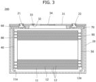
- FIG. 3 is a cross-sectional view schematically illustrating the battery cell according to embodiments of the present disclosure.
- a battery module according to embodiments of the present disclosure includes a housing 100, a battery cell 200, and a film cable 310.
- the housing 100 may form a schematic exterior of the battery module and function as a configuration which entirely supports the battery cell 200 and the film cable 310.
- the housing 100 may include a housing body 110 and a housing cover 120.
- the housing body 110 may be formed to have a box shape with a hollow therein and an open top.
- a cross-sectional shape of the housing body 110 may be changed to various shapes other than a quadrangular shape as illustrated in FIG. 1 .
- the housing cover 120 may open and close an internal space of the housing body 110.
- the housing cover 120 may be formed to have a plate or planar shape, or, in other words, a substantially plate shape and may be arranged to face an open top surface, opening or recess of the housing body 110.
- the housing cover 120 may be detachably coupled to the housing body 110 by various coupling methods such as screwing, mounting, bolting and fitting.
- the battery cell 200 may include at least one electrode assembly 10 wound with a separator 13, which is an insulator, interposed between a positive electrode 11 and a negative electrode 12, a case 20 in which the electrode assembly 10 is embedded, and a cap assembly 30 coupled to an opening of the case 20.
- a separator 13 which is an insulator
- the battery cell 200 a lithium-ion secondary battery with a prismatic shape will be described as an example.
- the present disclosure is not limited thereto, and the battery cell 200 may be a lithium polymer battery or cylindrical battery.
- the positive electrode 11 and the negative electrode 12 may include a coated part, which is an area in which an active material is coated on a current collector formed of a thin metal foil, and non-coated parts 11a and 12a, which are areas coating-free or, in other words, not coated with the active material.
- the positive electrode 11 and the negative electrode 12 may be wound with the separator 13, which is an insulator, interposed therebetween.
- the electrode assembly 10 may have a structure in which the positive and negative electrodes formed of a plurality of sheets are alternately stacked with the separator interposed therebetween.
- the case 20 may form the overall exterior of the battery cell 200 and may be made of a conductive metal such as aluminum, an aluminum alloy, or nickel-plated steel. In addition, the case 20 may provide a space in which the electrode assembly 10 is accommodated.
- the cap assembly 30 may include a cap plate 31 which covers the opening of the case 20, and the case 20 and the cap plate 31 may be made of a conductive material.
- the positive electrode and negative electrode terminals 21 and 22, which are electrically connected to the positive electrode 11 or the negative electrode 12, may be attached in such a way that they protrude outwards through the cap plate 31.
- outer circumferential surfaces of upper pillars of the positive electrode and negative electrode terminals 21 and 22 protruding outwards from the cap plate 31 may be threaded and fixed or secured to the cap plate 31 with nuts.
- positive electrode and negative electrode terminals 21 and 22 may be formed in a rivet structure and rivet-coupled, or coupled by being welded to the cap plate 31.
- the cap plate 31 may be formed of a thin plate and coupled to the opening of the case 20, an electrolyte injection port 32 into which a sealing stopper 33 may be installed or inserted may be formed in the cap plate 31, and a vent 34 on which a notch is formed may be installed.
- the vent 34 may be opened or closed in response to a change in internal pressure of the case 20.
- the vent 34 may maintain a closed state to seal the case 20 during normal operation of the electrode assembly 10.
- the vent 34 may be opened as the internal pressure of the case 20 increases to a set magnitude or higher due to overcharging, a fire, or the like and may discharge emissions such as flame and gas from the inside of the case 20 to the outside of the case 20.
- the positive electrode and negative electrode terminals 21 and 22 may be electrically connected to the current collector including first and second current collectors 40 and 50 (hereinafter referred to as "positive and negative current collectors") connected or bonded to the positive non-coated part 11a or the negative non-coated part 12a, for example by welding.
- the positive electrode and negative electrode terminals 21 and 22 may be coupled to the positive electrode and negative electrode current collectors 40 and 50 by welding.
- embodiments according to the present disclosure are not limited thereto, and the positive electrode and negative electrode terminals 21 and 22 and the positive electrode and negative electrode current collectors 40 and 50 may be formed by being coupled integrally.
- an insulating member may be installed between the electrode assembly 10 and the cap plate 31.
- the insulating member may include first and/or second lower insulating members 60 and 70, and each of the first and/or second lower insulating members 60 and 70 may be installed between the electrode assembly 10 and the cap plate 31.
- one end of a separation member which may be installed to face one side surface of the electrode assembly 10, may be installed between the insulating member and the positive electrode or negative electrode terminal 21 or 22.
- the separation member may include first and/or second separation members 80 and 90.
- first ends of the first and/or second separation members 80 and 90 which may be installed to face either side surface of the electrode assembly 10, respectively, may be installed between the first and second lower insulating members 60 and/or 70 and the positive electrode and negative electrode terminals 21 and 22.
- the positive electrode and negative electrode terminals 21 and 22 coupled by being welded to the positive electrode and negative electrode current collectors 40 and 50 may be coupled to first ends of the first and second lower insulating members 60 and 70 and the first and/or second separation members 80 and 90.
- a plurality of battery cells 200 may be provided.
- the plurality of battery cells 200 may be located inside the housing 100.
- the plurality of battery cells 200 may be arranged inside the housing 100.
- the number of battery cells 200 is not limited to that illustrated in FIG. 1 , and may be changed in design in various ways depending on the size or the like of the battery module.
- the film cable 310 is accommodated inside the housing.
- the film cable 310 is seated on the plurality of battery cells 200 and may extend substantially along a stacking direction of the battery cells 200.
- the film cable 310 may be a flexible flat cable (FFC) and may be used to measure voltages, temperatures, and the like of the plurality of battery cells 200 and transmit the measured voltages, temperatures, and the like to a battery management system (BMS).
- FFC flexible flat cable
- BMS battery management system
- the film cable 310 according to the present disclosure can block an overcurrent by performing a fuse function in order to prevent or reduce the overcurrent from flowing to a load or BMS when power is supplied and/or a signal is transmitted.
- FIG. 4 is a plan view schematically illustrating a film cable according to first embodiments of the present disclosure
- FIG. 5 is a cross-sectional view along a line V-V in FIG. 4 .
- the film cable 310 includes a conductor wire 311 and an overcurrent blocking unit 312.
- the conductor wire 311 may include a conductive metal material such as copper or silver.
- the conductor wire 311 may be formed in a plate shape or planar shape and formed to have a set length.
- the overcurrent blocking unit 312 is provided on the conductor wire 311.
- the overcurrent blocking unit 312 blocks the overcurrent flowing through the conductor wire 311 by reducing an allowable current of the conductor wire 311.
- the overcurrent blocking unit 312 may cause the conductor wire 311 to be melted and cut when a current exceeding a set current value flows through the conductor wire 311.
- the overcurrent blocking unit 312 may include an overcurrent blocking hole 312a passing through the conductor wire 311.
- the overcurrent blocking hole 312a may be formed through the conductor wire 311 in a thickness direction, or, in other words, perpendicular to an extension direction of the conductor wire 311.
- a plurality of overcurrent blocking holes 312a may be provided.
- the plurality of overcurrent blocking holes 312a may be arranged to be spaced apart from each other in an extension direction of the conductor wire 311. The arrangement may be equidistant or at different distances from each other.
- the overcurrent blocking hole 312a may be formed in a circular shape. Other shapes such as elliptical, triangular, rectangular or diamond-shaped may be also possible.
- the overcurrent blocking hole 312a may include a hollow portion 3121 and an edge portion 3122.
- the hollow portion 3121 may be formed in a hollow shape.
- the edge portion 3122 may be formed by drawing an arc along a circumference of the hollow portion 3121.
- a radius R of the hollow portion 3121 may be in a range of about 0.07 to about 0.09 mm.
- a distance D1 between a center point of the hollow portion 3121 and a center point of the adjacent hollow portion 3121 may be in a range of about 0.1 to about 0.3 mm.
- a total area of the plurality of overcurrent blocking holes 312a may be in a range of about 36 to about 42% of a total area of the conductor wire 311. For example, when the total area of the plurality of overcurrent blocking holes 312a is less than about 36% of the total area of the conductor wire 311, a current of about 1 A may flow through the conductor wire 311 for about 4 hours or more, a current of about 3 A may flow through the conductor wire 311 for more than about 5 seconds, and a current of about 4 A may flow through the conductor wire 311 for more than 1 second.
- a current of about 1 A may flow through the conductor wire 311 for less than about 4 hours
- a current of about 3 A may flow through the conductor wire 311 for about 5 seconds or less
- a current of about 4 A may flow through the conductor wire 311 for 1 second or less.
- the film cable 310 may further include an insulating member 400.
- the insulating member 400 may be provided to surround the conductor wire 311.
- the insulating member 400 may serve to protect the conductor wire 311 by covering the conductor wire 311.
- the insulating member 400 may be provided with a plurality of openings each communicating with each of the plurality of overcurrent blocking holes 312a. Each of the plurality of openings may be arranged to face each of the plurality of overcurrent blocking holes 312a.
- FIG. 6 is a perspective view schematically illustrating a film cable according to second embodiments of the present disclosure
- FIG. 7 is a cross-sectional view along a line VII-VII in FIG. 6 .
- the film cable 310 includes the conductor wire 311, the overcurrent blocking unit 312, and may include a potting resin 510.
- the description of the film cable 310 according to the first embodiments of the present disclosure can be applied to the remaining components of the film cable 310 according to the second embodiments of the present disclosure.
- the potting resin 510 may be filled in the overcurrent blocking hole 312a.
- the potting resin 510 may serve to protect the conductor wire 311 from an external impact.
- the potting resin 510 may include a silicone material.
- a ratio of a volume of the overcurrent blocking hole 312a to a volume of the potting resin 510 filled in the overcurrent blocking hole 312a may be in a range of about 1:3 to about 1:5.
- the conductor wire 311 may have a sufficient tensile strength of about 15 N or more
- the conductor wire 311 may have a reduced tensile strength of less than about 15 N.
- the potting resin 510 may include a first potting resin 511 and a second potting resin 512.
- the first potting resin 511 is filled in the overcurrent blocking hole 312a.
- the first potting resin 511 is filled in the overcurrent blocking hole 312a at a ratio of about 1:1 of the volume of the overcurrent blocking hole 312a.
- the second potting resin 512 may cover the overcurrent blocking hole 312a and the conductor wire 311 without being filled in the overcurrent blocking hole 312a anymore.
- the second potting resin 512 may be applied to a surface of the conductor wire 311 or the overcurrent blocking hole 312a is unfilled with respect to the second potting resin 512.
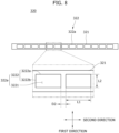
- FIG. 8 is a plan view schematically illustrating a film cable according to third embodiments of the present disclosure.
- a film cable 320 according to the third embodiments of the present disclosure may include a conductor wire 321 and an overcurrent blocking unit 322.
- the conductor wire 321 may include a conductive metal material such as copper or silver.
- the conductor wire 321 may be formed in a plate shape and formed to have a set length.
- the overcurrent blocking unit 322 is provided on the conductor wire 321.
- the overcurrent blocking unit 322 blocks the overcurrent flowing through the conductor wire 321 by reducing an allowable current of the conductor wire 321.
- the overcurrent blocking unit 322 may cause the conductor wire 321 to be melted and cut when a current exceeding a set current value flows through the conductor wire 321.
- the overcurrent blocking unit 322 may include an overcurrent blocking hole 322a passing through the conductor wire 321.
- the overcurrent blocking hole 322a may be formed through the conductor wire 321 in a thickness direction, or, in other words, perpendicular to an extension direction of the conductor wire 321.
- a plurality of overcurrent blocking holes 322a may be provided.
- the plurality of overcurrent blocking holes 322a may be arranged to be spaced apart from each other in an extension direction of the conductor wire 321. The arrangement may be equidistant or at different distances from each other.
- the overcurrent blocking hole 322a may be formed in a rectangular shape.
- the overcurrent blocking hole 322a may include a hollow portion 3221 and an edge portion 3222.
- the hollow portion 3221 may be formed in a hollow shape.
- the edge portion 3222 may be provided along a circumferential portion of the hollow portion 3221.
- the edge portion 3222 may include a first edge portion 3222a and a second edge portion 3222b.
- a pair of first edge portions 3222a may be provided and arranged to be spaced apart from each other in a first direction.
- the first direction may be a width direction of the conductor wire 321.
- the pair of first edge portions 3222a may be linearly arranged side by side.
- a pair of second edge portions 3222b may be provided and arranged to be spaced apart from each other in a second direction intersecting the first direction.
- the second direction may be an extension direction of the conductor wire 321.
- the pair of second edge portions 3222b may be linearly arranged side by side.
- the pair of second edge portions 3222b may be connected to the pair of first edge portions 3222a, respectively.
- a length L1 of the first edge portion 3222a may be formed to be more than a length L2 of the second edge portion. Therefore, the overcurrent blocking hole 322a may be formed in a rectangular shape with angled corners.
- a total area of the plurality of overcurrent blocking holes 322a may be in a range of about 36 to about 41% of a total area of the conductor wire 321. For example, when the total area of the plurality of overcurrent blocking holes 322a is less than about 36% of the total area of the conductor wire 321, a current of about 1 A may flow through the conductor wire 321 for about 4 hours or more, a current of about 3 A may flow through the conductor wire 321 for more than about 5 seconds, and a current of about 4 A may flow through the conductor wire 321 for more than 1 second.
- a current of about 1 A may flow through the conductor wire 321 for less than about 4 hours
- a current of about 3 A may flow through the conductor wire 321 for about 5 seconds or less
- a current of about 4 A may flow through the conductor wire 321 for 1 second or less.
- FIG. 9 is a perspective view schematically illustrating a film cable according to fourth embodiments of the present disclosure
- FIG. 10 is a cross-sectional view along a line X-X in FIG. 9 .
- the film cable 320 includes a conductor wire 321, an overcurrent blocking unit 322, and may include a potting resin 520.
- the description of the film cable 320 according to the third embodiments of the present disclosure can be applied to the remaining components of the film cable 320 according to the fourth embodiment of the present disclosure.
- the potting resin 520 may be filled in the overcurrent blocking hole 322a.
- the potting resin 520 may serve to protect the conductor wire 321 from an external impact.
- the potting resin 520 may include a silicone material.
- a ratio of a volume of the overcurrent blocking hole 322a to a volume of the potting resin 520 filled in the overcurrent blocking hole 322a may be in a range of about 1:3 to about 1:5.
- the conductor wire 321 may have a sufficient tensile strength of about 15 N or more
- the conductor wire 321 may have a reduced tensile strength of less than about 15 N.
- the potting resin 520 may include a first potting resin 521 and a second potting resin 522.
- the first potting resin 521 is filled in the overcurrent blocking hole 322a.
- the first potting resin 521 is filled in the overcurrent blocking hole 322a at a ratio of about 1:1 of the volume of the overcurrent blocking hole 322a.
- the second potting resin 522 may cover the overcurrent blocking hole 322a and the conductor wire 321 without being filled in the overcurrent blocking hole 322a anymore.
- the second potting resin 522 may be applied to a surface of the conductor wire 321 or the overcurrent blocking hole 322a is unfilled with respect to the second potting resin 522.
- FIG. 11 is a plan view schematically illustrating a film cable according to fifth embodiments of the present disclosure.
- a film cable 330 according to the fifth embodiments of the present disclosure may include a conductor wire 331 and an overcurrent blocking unit 332.
- the conductor wire 331 may include a conductive metal material such as copper or silver.
- the conductor wire 331 may be formed in a plate shape and formed to have a set length.
- the overcurrent blocking unit 332 is provided on the conductor wire 331.
- the overcurrent blocking unit 332 blocks the overcurrent flowing through the conductor wire 331 by reducing an allowable current of the conductor wire 331.
- the overcurrent blocking unit 332 may cause the conductor wire 331 to be melted and cut when a current exceeding a set current value flows through the conductor wire 331.
- the overcurrent blocking unit 332 may include an overcurrent blocking hole 332a passing through the conductor wire 331.
- the overcurrent blocking hole 332a may be formed through the conductor wire 331 in a thickness direction, or, in other words, perpendicular to an extension direction of the conductor wire 331.
- a plurality of overcurrent blocking holes 332a may be provided.
- the plurality of overcurrent blocking holes 332a may be arranged to be spaced apart from each other in an extension direction of the conductor wire 331. The arrangement may be equidistant or at different distances from each other.
- the overcurrent blocking hole 332a may be formed in a rectangular shape with each corner rounded.
- the overcurrent blocking hole 332a may include a hollow portion 3321 and an edge portion 3322.
- the hollow portion 3321 may be formed in a hollow shape.
- the edge portion 3322 may be provided along a circumferential portion of the hollow portion 3321.
- the edge portion 3322 may include a first edge portion 3322a, a second edge portion 3322b, and a connecting portion 3322c.
- a pair of first edge portions 3322a may be provided and arranged to be spaced apart from each other in a first direction.
- the first direction may be a width direction of the conductor wire 331.
- the pair of first edge portions 3322a may be linearly arranged side by side.
- a pair of second edge portions 3322b may be provided and arranged to be spaced apart from each other in a second direction intersecting the first direction.
- the second direction may be an extension direction of the conductor wire 331.
- the pair of second edge portions 3322b may be linearly arranged side by side.
- the pair of second edge portions 3322b may be connected to the pair of first edge portions 3322a, respectively.
- the connecting portions 3322c may connect the pair of first edge portions 3322a to the pair of second edge portions 3322b.
- the connecting portions 3322c may be located at each corner of the edge portion 3322 to connect the first edge portions 3322a to the second edge portions 3322b.
- the connecting portions 3322c may be formed to be rounded.
- a total area of the plurality of overcurrent blocking holes 332a may be in a range of about 37 to about 41% of a total area of the conductor wire 331. For example, when the total area of the plurality of overcurrent blocking holes 332a is less than about 37% of the total area of the conductor wire 331, a current of about 1 A may flow through the conductor wire 331 for about 4 hours or more, a current of about 3 A may flow through the conductor wire 331 for more than about 5 seconds, and a current of about 4 A may flow through the conductor wire 331 for more than 1 second.
- a current of about 1 A may flow through the conductor wire 331 for less than about 4 hours
- a current of about 3 A may flow through the conductor wire 331 for about 5 seconds or less
- a current of about 4 A may flow through the conductor wire 331 for 1 second or less.
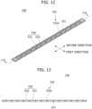
- FIG. 12 is a perspective view schematically illustrating a film cable according to sixth embodiments of the present disclosure
- FIG. 13 is a cross-sectional view along line XIII-XIII in FIG. 12 .
- the film cable according to the sixth embodiments of the present disclosure includes a conductor wire 331, an overcurrent blocking unit 332, and may include a potting resin 530.
- the description of the film cable 330 according to the fifth embodiments of the present disclosure can be applied to the remaining components of the film cable 330 according to the sixth embodiments of the present disclosure.
- the potting resin 530 may be filled in the overcurrent blocking hole 332a.
- the potting resin 530 may serve to protect the conductor wire 331 from an external impact.
- the potting resin 530 may include a silicone material.
- a ratio of a volume of the overcurrent blocking hole 332a to a volume of the potting resin 530 filled in the overcurrent blocking hole 332a may be in a range of about 1:3 to about 1:5.
- the conductor wire 331 may have a sufficient tensile strength of about 15 N or more
- the conductor wire 331 may have a low tensile strength of less than about 15 N.
- the potting resin 530 may include a first potting resin 531 and a second potting resin 532.
- the first potting resin 531 is filled in the overcurrent blocking hole 332a.
- the first potting resin 531 is filled in the overcurrent blocking hole 332a at a ratio of about 1:1 of the volume of the overcurrent blocking hole 332a.
- the second potting resin 532 may cover the overcurrent blocking hole 332a and the conductor wire 331 without being filled in the overcurrent blocking hole 332a anymore.
- the second potting resin 532 may be applied to a surface of the conductor wire 331 or the overcurrent blocking hole 332a is unfilled with respect to the second potting resin 532.
Landscapes
- Chemical & Material Sciences (AREA)
- Chemical Kinetics & Catalysis (AREA)
- Electrochemistry (AREA)
- General Chemical & Material Sciences (AREA)
- Engineering & Computer Science (AREA)
- Manufacturing & Machinery (AREA)
- Power Engineering (AREA)
- Microelectronics & Electronic Packaging (AREA)
- Connection Of Batteries Or Terminals (AREA)
Abstract
The present disclosure relates to a film cable including a conductor wire, and an overcurrent blocking unit provided on the conductor wire and configured to block an overcurrent flowing through the conductor wire by reducing an allowable current of the conductor wire. The present disclosure further relates to a battery module comprising the film cable according to the invention.
Description
- The present disclosure relates to a film cable and a battery module including the same.
- A secondary battery is a battery that can be charged and discharged, unlike a primary battery that cannot be recharged. Low-capacity secondary batteries are used in small portable electronic devices such as smartphones, feature phones, notebook computers, digital cameras, and camcorders, and high-capacity secondary batteries are widely used as power storage batteries and power sources for driving motors in hybrid and electric vehicles. Such a secondary battery includes an electrode assembly with a positive electrode and a negative electrode, a case for accommodating the electrode assembly, electrode terminals connected to the electrode assembly, and the like.
- The information described in the background of the present disclosure is merely disclosed for helping to understand the background of the present disclosure, and therefore it may contain information that does not constitute the related art.
- The invention is defined by the appended claims. The description that follows is subjected to this limitation. Any disclosure lying outside the scope of said claims is only intended for illustrative as well as comparative purposes.
- One or more embodiments include a film cable which may function as a fuse to block overcurrent, and a battery module including the same.
- These and other aspects and characteristics of embodiments according to of the present disclosure will be described in or will be apparent from the following description of some embodiments of the present disclosure.
- According to one or more embodiments, a film cable includes a conductor wire, and an overcurrent blocking unit provided on the conductor wire and configured to block an overcurrent flowing through the conductor wire by reducing an allowable current of the conductor wire.
- The overcurrent blocking unit may include an overcurrent blocking hole passing through the conductor wire.
- The overcurrent blocking hole may pass substantially perpendicular to an extension direction of the conductor wire.
- The overcurrent blocking hole may be formed in a circular shape or may be formed in other shapes such as elliptical, triangular, rectangular or diamond-shaped. A suitable combination of different shapes may also be selected. In this way, potential influences on tensile strength can be counteracted at the same time as saving material and improving overcurrent flowing protection. Suitable shapes and combinations thereof can reduce weak points and improve mechanical stability.
- A plurality of overcurrent blocking holes may be spaced apart from each other in an extension direction of the conductor wire.
- A total area of a plurality of overcurrent blocking holes may be in a range of 36% to 42% of a total area of the conductor wire.
- The film cable may further include an insulating member surrounding the conductor wire.
- The overcurrent blocking hole may include a hollow portion formed of a hollow, and an edge portion provided along a circumferential portion of the hollow portion. In other words, the overcurrent blocking hole may include a hollow portion formed of a cavity and an edge portion provided along a peripheral portion of the hollow portion.
- The hollow portion may have a circular cross-section or a cross-section of the hollow portion may have other shapes such as elliptical, triangular, rectangular or diamond-shaped.
- A radius of the hollow portion may be in a range of 0.07 to 0.09 mm.
- A distance between a center point of the hollow portion and a center point of an adjacent hollow portion may be in a range of 0.1 to 0.3 mm.
- An arrangement of the plurality of overcurrent blocking holes may be equidistant or may be at different distances from each other.
- The edge portion may include a pair of first edge portions spaced apart from each other in a first direction, and a pair of second edge portions spaced apart from each other in a second direction intersecting the first direction and connected to the pair of first edge portions.
- A length of the first edge portion may be greater than a length of the second edge portion.
- The edge portion may further include connecting portions connecting the pair of first edge portions to the pair of second edge portions and formed to be rounded.
- A distance between the second edge portion and the adjacent second edge portion may be in a range of 0.04 mm to 0.06 mm.
- The film cable may further include a potting resin filled in the overcurrent blocking hole or in at least one overcurrent blocking hole of the plurality of overcurrent blocking holes.
- A ratio of a volume of the overcurrent blocking hole or of at least one overcurrent blocking hole of the plurality of overcurrent blocking holes to a volume of the potting resin filled in the overcurrent blocking hole or in the at least one overcurrent blocking hole of the plurality of overcurrent blocking holes may have a range of 1:3 to 1:5.
- The potting resin may include a first potting resin filled in the overcurrent blocking hole or in at least one overcurrent blocking hole of the plurality of overcurrent blocking holes, and a second potting resin covering the overcurrent blocking hole or the at least one overcurrent blocking hole of the plurality of overcurrent blocking holes and the conductor wire without being filled in the overcurrent blocking hole or in the at least one overcurrent blocking hole of the plurality of overcurrent blocking holes anymore when the ratio of the volume of the overcurrent blocking hole or of the at least one overcurrent blocking hole of the plurality of overcurrent blocking holes to the volume of the first potting resin filled in the overcurrent blocking hole or in the at least one overcurrent blocking hole of the plurality of overcurrent blocking holes exceeds 1:1. In other words, the second potting resin may be applied to a surface of the conductor wire or the overcurrent blocking hole or the at least one overcurrent blocking hole of the plurality of overcurrent blocking holes is unfilled with respect to the second potting resin.
- According to one or more embodiments, a battery module according includes a housing, a plurality of battery cells in the housing, preferably accommodated in the housing, and the film cable in the housing, preferably accommodated in the housing, and seated on the plurality of battery cells.
- The film cable may extend substantially along a stacking direction of the battery cells.
- According to one or more embodiments of the present disclosure, by reducing an allowable current of a conductor wire by a plurality of overcurrent blocking holes spaced apart from each other in an extension direction of the conductor wire and formed in a range of about 36 to 42% of a total area of the conductor wire, it is possible to block an overcurrent flowing through the conductor wire and save a manufacturing cost of a film cable.
- In accordance with one or more embodiments of the present disclosure, by increasing a strength of the conductor wire by a potting resin filled in the overcurrent blocking hole, it may be possible to respond to vibration or an external impact.
- However, the effects obtainable by the present disclosure are not limited to the above-mentioned effects, and other technical effects not mentioned will be clearly understood by those skilled in the art from the following description of the present disclosure.
- The accompanying drawings in the present specification show embodiments of the present disclosure, and are illustrated to help further understand the technical concept, aspects and features of the present disclosure together with the detailed description of the present disclosure. Therefore, the present disclosure shall not be interpreted as being defined only by the aspects illustrated in the drawings.
-
FIG. 1 is an exploded perspective view schematically illustrating a battery module according to embodiments of the present disclosure; -
FIG. 2 is a perspective view schematically illustrating a battery cell according to embodiments of the present disclosure; -
FIG. 3 is a cross-sectional view schematically illustrating the battery cell according to embodiments of the present disclosure; -
FIG. 4 is a plan view schematically illustrating a film cable according to embodiments of the present disclosure; -
FIG. 5 is a cross-sectional view along a line V-V inFIG. 4 ; -
FIG. 6 is a perspective view schematically illustrating a film cable according to embodiments of the present disclosure; -
FIG. 7 is a cross-sectional view along a line VII-VII inFIG. 6 ; -
FIG. 8 is a plan view schematically illustrating a film cable according to embodiments of the present disclosure; -
FIG. 9 is a perspective view schematically illustrating a film cable according to embodiments of the present disclosure; -
FIG. 10 is a cross-sectional view along a line X-X inFIG. 9 ; -
FIG. 11 is a plan view schematically illustrating a film cable according to embodiments of the present disclosure; -
FIG. 12 is a perspective view schematically illustrating a film cable according to embodiments of the present disclosure; and -
FIG. 13 is a cross-sectional view along a line XIII-XIII inFIG. 12 . - Reference will now be made in detail to embodiments, examples of which are illustrated in the accompanying drawings, wherein like reference numerals refer to like elements throughout. In this regard, the present embodiments may have different forms and should not be construed as being limited to the descriptions set forth herein. Accordingly, the embodiments are merely described below, by referring to the figures, to explain aspects of the present description. As used herein, the term "and/or" includes any and all combinations of one or more of the associated listed items. Expressions such as "at least one of," if preceding a list of elements, modify the entire list of elements and do not modify the individual elements of the list.
- Hereinafter, embodiments of the present disclosure will be described, in further detail, with reference to the accompanying drawings. The terms or words used in this specification and claims should not be construed as being limited to the usual or dictionary meaning and should be interpreted as meaning and concept consistent with the technical idea of the present disclosure based on the principle that the inventor can be his/her own lexicographer to appropriately define the concept of the term.
- The embodiments described in this specification and the configurations shown in the drawings are provided as some example embodiments of the present disclosure and do not represent all of the technical ideas, aspects, and features of the present disclosure. Accordingly, it is to be understood that there may be various equivalents and modifications that may replace or modify the embodiments described herein at the time of filing this application.
- It is to be understood that when an element or layer is referred to as being "on," "connected to," or "coupled to" another element or layer, it may be directly on, connected, or coupled to the other element or layer or one or more intervening elements or layers may also be present. When an element or layer is referred to as being "directly on," "directly connected to," or "directly coupled to" another element or layer, there are no intervening elements or layers present. For example, when a first element is described as being "coupled" or "connected" to a second element, the first element may be directly coupled or connected to the second element or the first element may be indirectly coupled or connected to the second element via one or more intervening elements.
- In the figures, dimensions of the various elements, layers, etc. may be exaggerated for clarity of illustration. The same reference numerals designate the same or like elements. As used herein, the term "and/or" includes any and all combinations of one or more of the associated listed items. Further, the use of "may" when describing embodiments of the present disclosure relates to "one or more embodiments of the present disclosure." Expressions, such as "at least one of" and "any one of," when preceding a list of elements, modify the entire list of elements and do not modify the individual elements of the list. When phrases such as "at least one of A, B, and C," "at least one of A, B, or C," "at least one selected from a group of A, B, and C," or "at least one selected from among A, B, and C" are used to designate a list of elements A, B, and C, the phrase may refer to any and all suitable combinations or a subset of A, B, and C, such as A, B, C, A and B, A and C, B and C, or A and B and C. As used herein, the terms "use," "using," and "used" may be considered synonymous with the terms "utilize," "utilizing," and "utilized," respectively. As used herein, the terms "substantially," "about," and similar terms are used as terms of approximation and not as terms of degree, and are intended to account for the inherent variations in measured or calculated values that would be recognized by those of ordinary skill in the art.
- It is to be understood that, although the terms "first," "second," "third," etc. may be used herein to describe various elements, components, regions, layers, and/or sections, these elements, components, regions, layers, and/or sections should not be limited by these terms. These terms are used to distinguish one element, component, region, layer, or section from another element, component, region, layer, or section. Thus, a first element, component, region, layer, or section discussed below could be termed a second element, component, region, layer, or section without departing from the teachings of example embodiments.
- Spatially relative terms, such as "beneath," "below," "lower," "above," "upper," and the like, may be used herein for ease of description to describe one element or feature's relationship to another element(s) or feature(s) as illustrated in the figures. It is to be understood that the spatially relative terms are intended to encompass different orientations of the device in use or operation in addition to the orientation depicted in the figures. For example, if the device in the figures is turned over, elements described as "below" or "beneath" other elements or features would then be oriented "above" or "over" the other elements or features. Thus, the term "below" may encompass both an orientation of above and below. The device may be otherwise oriented (e.g., rotated 90 degrees or at other orientations), and the spatially relative descriptors used herein should be interpreted accordingly.
- The terminology used herein is for the purpose of describing embodiments of the present disclosure and is not intended to be limiting of the present disclosure. As used herein, the singular forms "a" and "an" are intended to include the plural forms as well, unless the context clearly indicates otherwise. It is to be further understood that the terms "includes," "including," "comprises," and/or "comprising," when used in this specification, specify the presence of stated features, integers, steps, operations, elements, and/or components but do not preclude the presence or addition of one or more other features, integers, steps, operations, elements, components, and/or groups thereof.
- Also, any numerical range disclosed and/or recited herein is intended to include all sub-ranges of the same numerical precision subsumed within the recited range. For example, a range of "1.0 to 10.0" is intended to include all subranges between (and including) the recited minimum value of 1.0 and the recited maximum value of 10.0, that is, having a minimum value equal to or greater than 1.0 and a maximum value equal to or less than 10.0, such as, for example, 2.4 to 7.6. Any maximum numerical limitation recited herein is intended to include all lower numerical limitations subsumed therein, and any minimum numerical limitation recited in this specification is intended to include all higher numerical limitations subsumed therein. Accordingly, applicant reserves the right to amend this specification, including the claims, to expressly recite any sub-range subsumed within the ranges expressly recited herein.
- References to two compared elements, features, etc. as being "the same" may mean that they are "substantially the same." Thus, the phrase "substantially the same" may include a case having a deviation that is considered low in the art, for example, a deviation of 5% or less. In addition, when a certain parameter is referred to as being uniform in a given region, it may mean that it is uniform in terms of an average.
- Throughout the specification, unless otherwise stated, each element may be singular or plural.
- When an arbitrary element is referred to as being arranged (or located or positioned) on the "above (or below)" or "on (or under)" a component, it may mean that the arbitrary element is placed in contact with the upper (or lower) surface of the component and may also mean that another component may be interposed between the component and any arbitrary element arranged (or located or positioned) on (or under) the component.
- In addition, it is to be understood that when an element is referred to as being "coupled," "linked," or "connected" to another element, the elements may be directly "coupled," "linked," or "connected" to each other, or one or more intervening elements may be present therebetween, through which the element may be "coupled," "linked," or "connected" to another element. In addition, when a part is referred to as being "electrically coupled" to another part, the part may be directly electrically connected to another part or one or more intervening parts may be present therebetween such that the part and the another part are indirectly electrically connected to each other.
- Throughout the specification, when "A and/or B" is stated, it means A, B, or A and B, unless otherwise stated. That is, "and/or" includes any or all combinations of a plurality of items enumerated. When "C to D" is stated, it means C or more and D or less, unless otherwise specified.
- The terms used in the present specification are for describing embodiments of the present disclosure and are not intended to limit the present disclosure.
-
FIG. 1 is an exploded perspective view schematically illustrating a battery module according to embodiments of the present disclosure,FIG. 2 is a perspective view schematically illustrating a battery cell according to embodiments of the present disclosure, andFIG. 3 is a cross-sectional view schematically illustrating the battery cell according to embodiments of the present disclosure. - Referring to
FIGS. 1 to 3 , a battery module according to embodiments of the present disclosure includes ahousing 100, abattery cell 200, and afilm cable 310. - The
housing 100 may form a schematic exterior of the battery module and function as a configuration which entirely supports thebattery cell 200 and thefilm cable 310. Thehousing 100 may include ahousing body 110 and ahousing cover 120. - The
housing body 110 may be formed to have a box shape with a hollow therein and an open top. A cross-sectional shape of thehousing body 110 may be changed to various shapes other than a quadrangular shape as illustrated inFIG. 1 . - The
housing cover 120 may open and close an internal space of thehousing body 110. Thehousing cover 120 may be formed to have a plate or planar shape, or, in other words, a substantially plate shape and may be arranged to face an open top surface, opening or recess of thehousing body 110. Thehousing cover 120 may be detachably coupled to thehousing body 110 by various coupling methods such as screwing, mounting, bolting and fitting. - The
battery cell 200 may include at least one electrode assembly 10 wound with aseparator 13, which is an insulator, interposed between apositive electrode 11 and anegative electrode 12, acase 20 in which the electrode assembly 10 is embedded, and a cap assembly 30 coupled to an opening of thecase 20. - For the
battery cell 200, a lithium-ion secondary battery with a prismatic shape will be described as an example. However, the present disclosure is not limited thereto, and thebattery cell 200 may be a lithium polymer battery or cylindrical battery. - The
positive electrode 11 and thenegative electrode 12 may include a coated part, which is an area in which an active material is coated on a current collector formed of a thin metal foil, andnon-coated parts - The
positive electrode 11 and thenegative electrode 12 may be wound with theseparator 13, which is an insulator, interposed therebetween. However, embodiments according to the present disclosure are not limited thereto, and the electrode assembly 10 may have a structure in which the positive and negative electrodes formed of a plurality of sheets are alternately stacked with the separator interposed therebetween. - The
case 20 may form the overall exterior of thebattery cell 200 and may be made of a conductive metal such as aluminum, an aluminum alloy, or nickel-plated steel. In addition, thecase 20 may provide a space in which the electrode assembly 10 is accommodated. - The cap assembly 30 may include a
cap plate 31 which covers the opening of thecase 20, and thecase 20 and thecap plate 31 may be made of a conductive material. Here, the positive electrode andnegative electrode terminals positive electrode 11 or thenegative electrode 12, may be attached in such a way that they protrude outwards through thecap plate 31. - In addition, outer circumferential surfaces of upper pillars of the positive electrode and
negative electrode terminals cap plate 31 may be threaded and fixed or secured to thecap plate 31 with nuts. - However, embodiments according to the present disclosure are not limited thereto, and the positive electrode and
negative electrode terminals cap plate 31. - In addition, the
cap plate 31 may be formed of a thin plate and coupled to the opening of thecase 20, anelectrolyte injection port 32 into which a sealingstopper 33 may be installed or inserted may be formed in thecap plate 31, and avent 34 on which a notch is formed may be installed. - The
vent 34 may be opened or closed in response to a change in internal pressure of thecase 20. In other words, thevent 34 may maintain a closed state to seal thecase 20 during normal operation of the electrode assembly 10. Thevent 34 may be opened as the internal pressure of thecase 20 increases to a set magnitude or higher due to overcharging, a fire, or the like and may discharge emissions such as flame and gas from the inside of thecase 20 to the outside of thecase 20. - The positive electrode and
negative electrode terminals current collectors 40 and 50 (hereinafter referred to as "positive and negative current collectors") connected or bonded to the positivenon-coated part 11a or the negativenon-coated part 12a, for example by welding. - For example, the positive electrode and
negative electrode terminals current collectors negative electrode terminals current collectors - In addition, an insulating member may be installed between the electrode assembly 10 and the
cap plate 31. Here, the insulating member may include first and/or second lower insulatingmembers members cap plate 31. - In addition, according to embodiments, one end of a separation member, which may be installed to face one side surface of the electrode assembly 10, may be installed between the insulating member and the positive electrode or
negative electrode terminal second separation members - Therefore, first ends of the first and/or
second separation members members 60 and/or 70 and the positive electrode andnegative electrode terminals - As a result, the positive electrode and
negative electrode terminals current collectors members second separation members - A plurality of
battery cells 200 may be provided. The plurality ofbattery cells 200 may be located inside thehousing 100. The plurality ofbattery cells 200 may be arranged inside thehousing 100. The number ofbattery cells 200 is not limited to that illustrated inFIG. 1 , and may be changed in design in various ways depending on the size or the like of the battery module. - The
film cable 310 is accommodated inside the housing. Thefilm cable 310 is seated on the plurality ofbattery cells 200 and may extend substantially along a stacking direction of thebattery cells 200. Thefilm cable 310 may be a flexible flat cable (FFC) and may be used to measure voltages, temperatures, and the like of the plurality ofbattery cells 200 and transmit the measured voltages, temperatures, and the like to a battery management system (BMS). Thefilm cable 310 according to the present disclosure can block an overcurrent by performing a fuse function in order to prevent or reduce the overcurrent from flowing to a load or BMS when power is supplied and/or a signal is transmitted. -
FIG. 4 is a plan view schematically illustrating a film cable according to first embodiments of the present disclosure, andFIG. 5 is a cross-sectional view along a line V-V inFIG. 4 . - Referring to
FIGS. 4 and 5 , thefilm cable 310 according to the first embodiments of the present disclosure includes aconductor wire 311 and anovercurrent blocking unit 312. - The
conductor wire 311 may include a conductive metal material such as copper or silver. Theconductor wire 311 may be formed in a plate shape or planar shape and formed to have a set length. - The
overcurrent blocking unit 312 is provided on theconductor wire 311. Theovercurrent blocking unit 312 blocks the overcurrent flowing through theconductor wire 311 by reducing an allowable current of theconductor wire 311. Theovercurrent blocking unit 312 may cause theconductor wire 311 to be melted and cut when a current exceeding a set current value flows through theconductor wire 311. - The
overcurrent blocking unit 312 may include anovercurrent blocking hole 312a passing through theconductor wire 311. Theovercurrent blocking hole 312a may be formed through theconductor wire 311 in a thickness direction, or, in other words, perpendicular to an extension direction of theconductor wire 311. A plurality ofovercurrent blocking holes 312a may be provided. The plurality ofovercurrent blocking holes 312a may be arranged to be spaced apart from each other in an extension direction of theconductor wire 311. The arrangement may be equidistant or at different distances from each other. - The
overcurrent blocking hole 312a may be formed in a circular shape. Other shapes such as elliptical, triangular, rectangular or diamond-shaped may be also possible. Theovercurrent blocking hole 312a may include ahollow portion 3121 and anedge portion 3122. - The
hollow portion 3121 may be formed in a hollow shape. Theedge portion 3122 may be formed by drawing an arc along a circumference of thehollow portion 3121. - When a length of the
conductor wire 311 is about 5 mm and a width is about 0.25 mm, a radius R of thehollow portion 3121 may be in a range of about 0.07 to about 0.09 mm. A distance D1 between a center point of thehollow portion 3121 and a center point of the adjacenthollow portion 3121 may be in a range of about 0.1 to about 0.3 mm. - A total area of the plurality of
overcurrent blocking holes 312a may be in a range of about 36 to about 42% of a total area of theconductor wire 311. For example, when the total area of the plurality ofovercurrent blocking holes 312a is less than about 36% of the total area of theconductor wire 311, a current of about 1 A may flow through theconductor wire 311 for about 4 hours or more, a current of about 3 A may flow through theconductor wire 311 for more than about 5 seconds, and a current of about 4 A may flow through theconductor wire 311 for more than 1 second. - When the total area of the plurality of
overcurrent blocking holes 312a exceeds about 42% of the total area of theconductor wire 311, a current of about 1 A may flow through theconductor wire 311 for less than about 4 hours, a current of about 3 A may flow through theconductor wire 311 for about 5 seconds or less, and a current of about 4 A may flow through theconductor wire 311 for 1 second or less. - The
film cable 310 according to embodiments of the present disclosure may further include an insulatingmember 400. The insulatingmember 400 may be provided to surround theconductor wire 311. The insulatingmember 400 may serve to protect theconductor wire 311 by covering theconductor wire 311. - The insulating
member 400 may be provided with a plurality of openings each communicating with each of the plurality ofovercurrent blocking holes 312a. Each of the plurality of openings may be arranged to face each of the plurality ofovercurrent blocking holes 312a. -
FIG. 6 is a perspective view schematically illustrating a film cable according to second embodiments of the present disclosure, andFIG. 7 is a cross-sectional view along a line VII-VII inFIG. 6 . - Referring to
FIGS. 6 and 7 , thefilm cable 310 according to the second embodiments of the present disclosure includes theconductor wire 311, theovercurrent blocking unit 312, and may include apotting resin 510. - In describing the
film cable 310 according to the second embodiments of the present disclosure, only thepotting resin 510, which is not described in thefilm cable 310 according to the first embodiments of the present disclosure, will be described in more detail. - The description of the
film cable 310 according to the first embodiments of the present disclosure can be applied to the remaining components of thefilm cable 310 according to the second embodiments of the present disclosure. - The
potting resin 510 may be filled in theovercurrent blocking hole 312a. Thepotting resin 510 may serve to protect theconductor wire 311 from an external impact. Thepotting resin 510 may include a silicone material. - A ratio of a volume of the
overcurrent blocking hole 312a to a volume of thepotting resin 510 filled in theovercurrent blocking hole 312a may be in a range of about 1:3 to about 1:5. For example, when the ratio of the volume of theovercurrent blocking hole 312a to the volume of thepotting resin 510 filled in theovercurrent blocking hole 312a is about 1:3 or more, theconductor wire 311 may have a sufficient tensile strength of about 15 N or more, and when the ratio of the volume of theovercurrent blocking hole 312a to the volume of thepotting resin 510 filled in theovercurrent blocking hole 312a is about 1:1, theconductor wire 311 may have a reduced tensile strength of less than about 15 N. - The
potting resin 510 may include afirst potting resin 511 and asecond potting resin 512. - The
first potting resin 511 is filled in theovercurrent blocking hole 312a. In other words, thefirst potting resin 511 is filled in theovercurrent blocking hole 312a at a ratio of about 1:1 of the volume of theovercurrent blocking hole 312a. - When the ratio of the volume of the
overcurrent blocking hole 312a to the volume of thefirst potting resin 511 filled in theovercurrent blocking hole 312a exceeds about 1:1, thesecond potting resin 512 may cover theovercurrent blocking hole 312a and theconductor wire 311 without being filled in theovercurrent blocking hole 312a anymore. In other words, thesecond potting resin 512 may be applied to a surface of theconductor wire 311 or theovercurrent blocking hole 312a is unfilled with respect to thesecond potting resin 512. -
FIG. 8 is a plan view schematically illustrating a film cable according to third embodiments of the present disclosure. Referring toFIG. 8 , afilm cable 320 according to the third embodiments of the present disclosure may include aconductor wire 321 and anovercurrent blocking unit 322. - The
conductor wire 321 may include a conductive metal material such as copper or silver. Theconductor wire 321 may be formed in a plate shape and formed to have a set length. - The
overcurrent blocking unit 322 is provided on theconductor wire 321. Theovercurrent blocking unit 322 blocks the overcurrent flowing through theconductor wire 321 by reducing an allowable current of theconductor wire 321. Theovercurrent blocking unit 322 may cause theconductor wire 321 to be melted and cut when a current exceeding a set current value flows through theconductor wire 321. - The
overcurrent blocking unit 322 may include anovercurrent blocking hole 322a passing through theconductor wire 321. Theovercurrent blocking hole 322a may be formed through theconductor wire 321 in a thickness direction, or, in other words, perpendicular to an extension direction of theconductor wire 321. A plurality ofovercurrent blocking holes 322a may be provided. The plurality ofovercurrent blocking holes 322a may be arranged to be spaced apart from each other in an extension direction of theconductor wire 321. The arrangement may be equidistant or at different distances from each other. - The
overcurrent blocking hole 322a may be formed in a rectangular shape. Theovercurrent blocking hole 322a may include ahollow portion 3221 and anedge portion 3222. Thehollow portion 3221 may be formed in a hollow shape. - The
edge portion 3222 may be provided along a circumferential portion of thehollow portion 3221. Theedge portion 3222 may include afirst edge portion 3222a and asecond edge portion 3222b. - A pair of
first edge portions 3222a may be provided and arranged to be spaced apart from each other in a first direction. Here, the first direction may be a width direction of theconductor wire 321. The pair offirst edge portions 3222a may be linearly arranged side by side. - A pair of
second edge portions 3222b may be provided and arranged to be spaced apart from each other in a second direction intersecting the first direction. Here, the second direction may be an extension direction of theconductor wire 321. The pair ofsecond edge portions 3222b may be linearly arranged side by side. - The pair of
second edge portions 3222b may be connected to the pair offirst edge portions 3222a, respectively. A length L1 of thefirst edge portion 3222a may be formed to be more than a length L2 of the second edge portion. Therefore, theovercurrent blocking hole 322a may be formed in a rectangular shape with angled corners. - When the length of the
conductor wire 321 is about 5 mm, the width is about 0.25 mm, and the length of thefirst edge portion 3222a may be about 0.3 mm, and when the length of thesecond edge portion 3222b is about 0.15 mm, a distance D2 between thesecond edge portion 3222b and the adjacentsecond edge portion 3222b may be in a range of about 0.04 to about 0.06 mm. - A total area of the plurality of
overcurrent blocking holes 322a may be in a range of about 36 to about 41% of a total area of theconductor wire 321. For example, when the total area of the plurality ofovercurrent blocking holes 322a is less than about 36% of the total area of theconductor wire 321, a current of about 1 A may flow through theconductor wire 321 for about 4 hours or more, a current of about 3 A may flow through theconductor wire 321 for more than about 5 seconds, and a current of about 4 A may flow through theconductor wire 321 for more than 1 second. - When the total area of the plurality of
overcurrent blocking holes 322a exceeds about 41% of the total area of theconductor wire 321, a current of about 1 A may flow through theconductor wire 321 for less than about 4 hours, a current of about 3 A may flow through theconductor wire 321 for about 5 seconds or less, and a current of about 4 A may flow through theconductor wire 321 for 1 second or less. -
FIG. 9 is a perspective view schematically illustrating a film cable according to fourth embodiments of the present disclosure, andFIG. 10 is a cross-sectional view along a line X-X inFIG. 9 . - Referring to
FIGS. 9 and 10 , thefilm cable 320 according to the fourth embodiments of the present disclosure includes aconductor wire 321, anovercurrent blocking unit 322, and may include apotting resin 520. - In describing the
film cable 320 according to the fourth embodiments of the present disclosure, only thepotting resin 520, which is not described in thefilm cable 320 according to the third embodiment of the present disclosure, will be described. - The description of the
film cable 320 according to the third embodiments of the present disclosure can be applied to the remaining components of thefilm cable 320 according to the fourth embodiment of the present disclosure. - The
potting resin 520 may be filled in theovercurrent blocking hole 322a. Thepotting resin 520 may serve to protect theconductor wire 321 from an external impact. Thepotting resin 520 may include a silicone material. - A ratio of a volume of the
overcurrent blocking hole 322a to a volume of thepotting resin 520 filled in theovercurrent blocking hole 322a may be in a range of about 1:3 to about 1:5. For example, when the ratio of the volume of theovercurrent blocking hole 322a to the volume of thepotting resin 520 filled in theovercurrent blocking hole 322a is about 1:3 or more, theconductor wire 321 may have a sufficient tensile strength of about 15 N or more, and when the ratio of the volume of theovercurrent blocking hole 322a to the volume of thepotting resin 520 filled in theovercurrent blocking hole 322a is about 1:1, theconductor wire 321 may have a reduced tensile strength of less than about 15 N. - The
potting resin 520 may include afirst potting resin 521 and asecond potting resin 522. - The
first potting resin 521 is filled in theovercurrent blocking hole 322a. In other words, thefirst potting resin 521 is filled in theovercurrent blocking hole 322a at a ratio of about 1:1 of the volume of theovercurrent blocking hole 322a. - When the ratio of the volume of the
overcurrent blocking hole 322a to the volume of thefirst potting resin 521 filled in theovercurrent blocking hole 322a exceeds about 1:1, thesecond potting resin 522 may cover theovercurrent blocking hole 322a and theconductor wire 321 without being filled in theovercurrent blocking hole 322a anymore. In other words, thesecond potting resin 522 may be applied to a surface of theconductor wire 321 or theovercurrent blocking hole 322a is unfilled with respect to thesecond potting resin 522. -
FIG. 11 is a plan view schematically illustrating a film cable according to fifth embodiments of the present disclosure. Referring toFIG. 11 , afilm cable 330 according to the fifth embodiments of the present disclosure may include aconductor wire 331 and anovercurrent blocking unit 332. - The
conductor wire 331 may include a conductive metal material such as copper or silver. Theconductor wire 331 may be formed in a plate shape and formed to have a set length. - The
overcurrent blocking unit 332 is provided on theconductor wire 331. Theovercurrent blocking unit 332 blocks the overcurrent flowing through theconductor wire 331 by reducing an allowable current of theconductor wire 331. Theovercurrent blocking unit 332 may cause theconductor wire 331 to be melted and cut when a current exceeding a set current value flows through theconductor wire 331. - The
overcurrent blocking unit 332 may include anovercurrent blocking hole 332a passing through theconductor wire 331. Theovercurrent blocking hole 332a may be formed through theconductor wire 331 in a thickness direction, or, in other words, perpendicular to an extension direction of theconductor wire 331. A plurality ofovercurrent blocking holes 332a may be provided. The plurality ofovercurrent blocking holes 332a may be arranged to be spaced apart from each other in an extension direction of theconductor wire 331. The arrangement may be equidistant or at different distances from each other. - The
overcurrent blocking hole 332a may be formed in a rectangular shape with each corner rounded. Theovercurrent blocking hole 332a may include ahollow portion 3321 and anedge portion 3322. Thehollow portion 3321 may be formed in a hollow shape. - The
edge portion 3322 may be provided along a circumferential portion of thehollow portion 3321. Theedge portion 3322 may include afirst edge portion 3322a, asecond edge portion 3322b, and a connectingportion 3322c. - A pair of
first edge portions 3322a may be provided and arranged to be spaced apart from each other in a first direction. Here, the first direction may be a width direction of theconductor wire 331. The pair offirst edge portions 3322a may be linearly arranged side by side. - A pair of
second edge portions 3322b may be provided and arranged to be spaced apart from each other in a second direction intersecting the first direction. Here, the second direction may be an extension direction of theconductor wire 331. The pair ofsecond edge portions 3322b may be linearly arranged side by side. The pair ofsecond edge portions 3322b may be connected to the pair offirst edge portions 3322a, respectively. - The connecting
portions 3322c may connect the pair offirst edge portions 3322a to the pair ofsecond edge portions 3322b. The connectingportions 3322c may be located at each corner of theedge portion 3322 to connect thefirst edge portions 3322a to thesecond edge portions 3322b. The connectingportions 3322c may be formed to be rounded. - A length L3 of the
first edge portion 3322a may be formed to be more than a length L4 of thesecond edge portion 3322b. Therefore, theovercurrent blocking hole 332a may be formed in a rectangular shape with each corner rounded. - When the length of the
conductor wire 331 is about 5 mm, the width is about 0.25 mm, and the length of thefirst edge portion 3322a may be about 0.3 mm, and when the length of thesecond edge portion 3322b is about 0.15 mm, a distance D3 between thesecond edge portion 3322b and the adjacentsecond edge portion 3322b may be in a range of about 0.04 to about 0.06 mm. - A total area of the plurality of
overcurrent blocking holes 332a may be in a range of about 37 to about 41% of a total area of theconductor wire 331. For example, when the total area of the plurality ofovercurrent blocking holes 332a is less than about 37% of the total area of theconductor wire 331, a current of about 1 A may flow through theconductor wire 331 for about 4 hours or more, a current of about 3 A may flow through theconductor wire 331 for more than about 5 seconds, and a current of about 4 A may flow through theconductor wire 331 for more than 1 second. - When the total area of the plurality of
overcurrent blocking holes 332a exceeds about 41% of the total area of theconductor wire 331, a current of about 1 A may flow through theconductor wire 331 for less than about 4 hours, a current of about 3 A may flow through theconductor wire 331 for about 5 seconds or less, and a current of about 4 A may flow through theconductor wire 331 for 1 second or less. -
FIG. 12 is a perspective view schematically illustrating a film cable according to sixth embodiments of the present disclosure, andFIG. 13 is a cross-sectional view along line XIII-XIII inFIG. 12 . - Referring to
FIGS. 12 and 13 , the film cable according to the sixth embodiments of the present disclosure includes aconductor wire 331, anovercurrent blocking unit 332, and may include apotting resin 530. - In describing the
film cable 330 according to the sixth embodiments of the present disclosure, only thepotting resin 530, which is not described in thefilm cable 330 according to the fifth embodiments of the present disclosure, will be described. - The description of the
film cable 330 according to the fifth embodiments of the present disclosure can be applied to the remaining components of thefilm cable 330 according to the sixth embodiments of the present disclosure. - The
potting resin 530 may be filled in theovercurrent blocking hole 332a. Thepotting resin 530 may serve to protect theconductor wire 331 from an external impact. Thepotting resin 530 may include a silicone material. - A ratio of a volume of the
overcurrent blocking hole 332a to a volume of thepotting resin 530 filled in theovercurrent blocking hole 332a may be in a range of about 1:3 to about 1:5. For example, when the ratio of the volume of theovercurrent blocking hole 332a to the volume of thepotting resin 530 filled in theovercurrent blocking hole 332a is about 1:3 or more, theconductor wire 331 may have a sufficient tensile strength of about 15 N or more, and when the ratio of the volume of theovercurrent blocking hole 332a to the volume of thepotting resin 530 filled in theovercurrent blocking hole 332a is about 1:1, theconductor wire 331 may have a low tensile strength of less than about 15 N. - The
potting resin 530 may include afirst potting resin 531 and asecond potting resin 532. - The
first potting resin 531 is filled in theovercurrent blocking hole 332a. In other words, thefirst potting resin 531 is filled in theovercurrent blocking hole 332a at a ratio of about 1:1 of the volume of theovercurrent blocking hole 332a. - When the ratio of the volume of the
overcurrent blocking hole 332a to the volume of thefirst potting resin 531 filled in theovercurrent blocking hole 332a exceeds about 1:1, thesecond potting resin 532 may cover theovercurrent blocking hole 332a and theconductor wire 331 without being filled in theovercurrent blocking hole 332a anymore. In other words, thesecond potting resin 532 may be applied to a surface of theconductor wire 331 or theovercurrent blocking hole 332a is unfilled with respect to thesecond potting resin 532. - While aspects of some embodiments of the present disclosure have been described with reference to embodiments shown in the drawings, these embodiments are merely illustrative and it should be understood that various modifications and equivalent other embodiments can be derived by those skilled in the art on the basis of the embodiments.
- Therefore, the technical scope of the present disclosure should be defined by the appended claims, and their equivalents.
Claims (15)
- A film cable (310, 320, 330) comprising:a conductor wire (311, 321, 331); andan overcurrent blocking unit (312, 322, 332) provided on the conductor wire (311, 321, 331) and configured to block an overcurrent flowing through the conductor wire (311, 321, 331) by reducing an allowable current of the conductor wire (311, 321, 331).
- The film cable (310, 320, 330) as claimed in claim 1, wherein the overcurrent blocking unit (312, 322, 332) comprises an overcurrent blocking hole (312a, 322a, 332a) passing through the conductor wire (311, 321, 331).
- The film cable (310, 320, 330) as claimed in claim 2, wherein a plurality of overcurrent blocking holes (312a, 322a, 332a) are spaced apart from each other in an extension direction of the conductor wire (311, 321, 331).
- The film cable (310, 320, 330) as claimed in claim 2 or 3, wherein a total area of a plurality of overcurrent blocking holes (312a, 322a, 332a) is in a range of 36% to 42% of a total area of the conductor wire (311, 321, 331).
- The film cable (310, 320, 330) as claimed in any of claims 2 to 4, wherein the overcurrent blocking hole (312a, 322a, 332a) or at least one overcurrent blocking hole (312a, 322a, 332a) of the plurality of overcurrent blocking holes (312a, 322a, 332a) comprises:a hollow portion (3121, 3221, 3321) formed of a hollow; andan edge portion (3122, 3222, 3322) provided along a circumferential portion of the hollow portion (3121, 3221, 3321).
- The film cable (310, 320, 330) as claimed in claim 5, wherein a radius of the hollow portion (3121, 3221, 3321) is in a range of 0.07 mm to 0.09 mm.
- The film cable (310, 320, 330) as claimed in claim 5 or 6, wherein a distance between a center point of the hollow portion (3121, 3221, 3321) and a center point of an adjacent hollow portion (3121, 3221, 3321) is in a range of 0.1 to 0.3 mm.
- The film cable (310, 320, 330) as claimed in any of claims 5 to 7, wherein the edge portion (3122, 3222, 3322) comprises:a pair of first edge portions (3222a, 3322a) spaced apart from each other in a first direction; anda pair of second edge portions (3222b, 3322b) spaced apart from each other in a second direction intersecting the first direction and connected to the pair of first edge portions (3222a, 3322a).
- The film cable (310, 320, 330) as claimed in claim 8, wherein a length of the first edge portion (3222a, 3322a) is greater than a length of the second edge portion (3222b, 3322b).
- The film cable (310, 320, 330) as claimed in claim 8 or 9, wherein the edge portion (3122, 3222, 3322) further comprises connecting portions (3322c) connecting the pair of first edge portions (3222a, 3322a) to the pair of second edge portions (3222b, 3322b) and formed to be rounded.
- The film cable (310, 320, 330) as claimed in any of claims 8 to 10, wherein a distance between the second edge portion (3222b, 3322b) and the adjacent second edge portion (3222b, 3322b) is in a range of 0.04 mm to 0.06 mm.
- The film cable (310, 320, 330) as claimed in any of claims 2 to 11, further comprising a potting resin (510, 520, 530) filled in the overcurrent blocking hole (312a, 322a, 332a) or in at least one overcurrent blocking hole (312a, 322a, 332a) of the plurality of overcurrent blocking holes (312a, 322a, 332a).
- The film cable (310, 320, 330) as claimed in claim 12, wherein a ratio of a volume of the overcurrent blocking hole (312a, 322a, 332a) or of at least one overcurrent blocking hole (312a, 322a, 332a) of the plurality of overcurrent blocking holes (312a, 322a, 332a) to a volume of the potting resin (510, 520, 530) filled in the overcurrent blocking hole (312a, 322a, 332a) or in the at least one overcurrent blocking hole (312a, 322a, 332a) has a range of 1:3 to 1:5.
- The film cable (310, 320, 330) as claimed in claim 12 or 13, wherein the potting resin (510, 520, 530) comprises:a first potting resin (511, 521, 531) filled in the overcurrent blocking hole (312a, 322a, 332a) or in at least one overcurrent blocking hole (312a, 322a, 332a) of the plurality of overcurrent blocking holes (312a, 322a, 332a); anda second potting resin (512, 522, 532) covering the overcurrent blocking hole (312a, 322a, 332a) or the at least one overcurrent blocking hole (312a, 322a, 332a) and the conductor wire (311, 321, 331) without being filled in the overcurrent blocking hole (312a, 322a, 332a) or in the at least one overcurrent blocking hole (312a, 322a, 332a) anymore when the ratio of the volume of the overcurrent blocking hole (312a, 322a, 332a) or of the at least one overcurrent blocking hole (312a, 322a, 332a) to the volume of the first potting resin (511, 521, 531) filled in the overcurrent blocking hole (312a, 322a, 332a) or in the at least one overcurrent blocking hole (312a, 322a, 332a) exceeds 1:1.
- A battery module comprising:a housing (100);a plurality of battery cells (200) in the housing (100); andthe film cable (310, 320, 330) as claimed in any of claims 1 to 14 in the housing (100) and seated on the plurality of battery cells (200).
Applications Claiming Priority (1)
| Application Number | Priority Date | Filing Date | Title |
|---|---|---|---|
| KR1020230174425A KR20250085298A (en) | 2023-12-05 | 2023-12-05 | Film cable and battery module including the same |
Publications (1)
| Publication Number | Publication Date |
|---|---|
| EP4567854A1 true EP4567854A1 (en) | 2025-06-11 |
Family
ID=92043110
Family Applications (1)
| Application Number | Title | Priority Date | Filing Date |
|---|---|---|---|
| EP24190913.4A Pending EP4567854A1 (en) | 2023-12-05 | 2024-07-25 | Film cable and battery module including the same |
Country Status (4)
| Country | Link |
|---|---|
| US (1) | US20250183682A1 (en) |
| EP (1) | EP4567854A1 (en) |
| KR (1) | KR20250085298A (en) |
| CN (1) | CN120108817A (en) |
Citations (3)
| Publication number | Priority date | Publication date | Assignee | Title |
|---|---|---|---|---|
| CH279454A (en) * | 1948-06-18 | 1951-11-30 | Ag Weber | Fuse with fusible conductors. |
| US3523265A (en) * | 1967-03-30 | 1970-08-04 | English Electric Co Ltd | Fuse elements |
| US20170263407A1 (en) * | 2014-11-14 | 2017-09-14 | Littelfuse, Inc. | High-current fuse with endbell assembly |
Family Cites Families (1)
| Publication number | Priority date | Publication date | Assignee | Title |
|---|---|---|---|---|
| JP7339252B2 (en) * | 2018-07-10 | 2023-09-05 | 三洋電機株式会社 | FLEXIBLE FLAT CABLE WITH PROTECTIVE ELEMENT MOUNTING, BATTERY MODULE AND METHOD FOR MANUFACTURING FLEXIBLE FLAT CABLE WITH PROTECTIVE ELEMENT MOUNTING |
-
2023
- 2023-12-05 KR KR1020230174425A patent/KR20250085298A/en active Pending
-
2024
- 2024-07-15 CN CN202410942728.XA patent/CN120108817A/en active Pending
- 2024-07-15 US US18/773,264 patent/US20250183682A1/en active Pending
- 2024-07-25 EP EP24190913.4A patent/EP4567854A1/en active Pending
Patent Citations (3)
| Publication number | Priority date | Publication date | Assignee | Title |
|---|---|---|---|---|
| CH279454A (en) * | 1948-06-18 | 1951-11-30 | Ag Weber | Fuse with fusible conductors. |
| US3523265A (en) * | 1967-03-30 | 1970-08-04 | English Electric Co Ltd | Fuse elements |
| US20170263407A1 (en) * | 2014-11-14 | 2017-09-14 | Littelfuse, Inc. | High-current fuse with endbell assembly |
Also Published As
| Publication number | Publication date |
|---|---|
| KR20250085298A (en) | 2025-06-12 |
| CN120108817A (en) | 2025-06-06 |
| US20250183682A1 (en) | 2025-06-05 |
Similar Documents
| Publication | Publication Date | Title |
|---|---|---|
| EP3451418B1 (en) | Secondary battery | |
| EP3544078B1 (en) | Secondary battery | |
| US10236494B2 (en) | Secondary battery | |
| KR101576597B1 (en) | Secondary battery and battery pack including the same | |
| EP4567854A1 (en) | Film cable and battery module including the same | |
| EP4274017B1 (en) | Pouch-shaped battery cell including sensing member and battery module including the same | |
| EP4564547A1 (en) | Battery cell and battery module including the same | |
| US20250293385A1 (en) | Battery cell and battery module including the same | |
| EP4571950A1 (en) | Secondary battery | |
| US20240332685A1 (en) | Secondary battery | |
| EP4679591A1 (en) | Battery module | |
| US20250293392A1 (en) | Battery module | |
| US20260066441A1 (en) | Battery cell and battery module including the same | |
| US20250364702A1 (en) | Secondary battery | |
| US20260104472A1 (en) | Management module and battery module including the same | |
| US20260031449A1 (en) | Cap assembly and secondary battery including same | |
| US20260128454A1 (en) | Secondary battery | |
| EP4683050A1 (en) | Secondary battery and method of manufacturing same | |
| EP4697468A1 (en) | Battery module | |
| EP4576377A1 (en) | Battery pack and vehicle comprising same | |
| EP4693674A1 (en) | Battery module | |
| EP4366040A1 (en) | Secondary battery and battery module including the same | |
| US20260074378A1 (en) | Busbar holder and battery module including same | |
| EP4730507A1 (en) | Battery structure | |
| US8492014B2 (en) | Secondary battery |
Legal Events
| Date | Code | Title | Description |
|---|---|---|---|
| PUAI | Public reference made under article 153(3) epc to a published international application that has entered the european phase |
Free format text: ORIGINAL CODE: 0009012 |
|
| STAA | Information on the status of an ep patent application or granted ep patent |
Free format text: STATUS: REQUEST FOR EXAMINATION WAS MADE |
|
| 17P | Request for examination filed |
Effective date: 20240725 |
|
| AK | Designated contracting states |
Kind code of ref document: A1 Designated state(s): AL AT BE BG CH CY CZ DE DK EE ES FI FR GB GR HR HU IE IS IT LI LT LU LV MC ME MK MT NL NO PL PT RO RS SE SI SK SM TR |