EP4567838A1 - Bushing for medium or high voltage applications and method for manufacturing the bushing - Google Patents
Bushing for medium or high voltage applications and method for manufacturing the bushing Download PDFInfo
- Publication number
- EP4567838A1 EP4567838A1 EP23215294.2A EP23215294A EP4567838A1 EP 4567838 A1 EP4567838 A1 EP 4567838A1 EP 23215294 A EP23215294 A EP 23215294A EP 4567838 A1 EP4567838 A1 EP 4567838A1
- Authority
- EP
- European Patent Office
- Prior art keywords
- housing
- bushing
- shell parts
- insulation material
- primary conductor
- Prior art date
- Legal status (The legal status is an assumption and is not a legal conclusion. Google has not performed a legal analysis and makes no representation as to the accuracy of the status listed.)
- Pending
Links
Images

Classifications
-
- H—ELECTRICITY
- H01—ELECTRIC ELEMENTS
- H01B—CABLES; CONDUCTORS; INSULATORS; SELECTION OF MATERIALS FOR THEIR CONDUCTIVE, INSULATING OR DIELECTRIC PROPERTIES
- H01B7/00—Insulated conductors or cables characterised by their form
- H01B7/42—Insulated conductors or cables characterised by their form with arrangements for heat dissipation or conduction
-
- H—ELECTRICITY
- H01—ELECTRIC ELEMENTS
- H01B—CABLES; CONDUCTORS; INSULATORS; SELECTION OF MATERIALS FOR THEIR CONDUCTIVE, INSULATING OR DIELECTRIC PROPERTIES
- H01B17/00—Insulators or insulating bodies characterised by their form
- H01B17/26—Lead-in insulators; Lead-through insulators
- H01B17/28—Capacitor type
-
- H—ELECTRICITY
- H01—ELECTRIC ELEMENTS
- H01B—CABLES; CONDUCTORS; INSULATORS; SELECTION OF MATERIALS FOR THEIR CONDUCTIVE, INSULATING OR DIELECTRIC PROPERTIES
- H01B17/00—Insulators or insulating bodies characterised by their form
- H01B17/54—Insulators or insulating bodies characterised by their form having heating or cooling devices
Definitions
- the present invention relates to a bushing for medium or high voltage switching devices.
- the invention further relates to a method for manufacturing a bushing.
- thermosetting resin such as epoxy
- the purpose of the insulation has been to prevent electric discharges between the conductor and the wall of a container through which the bushing protrudes.
- the thermosetting resin has been provided with a sufficiently high thickness to provide a satisfactory functionality in this respect.
- molding thick solid bodies of thermosetting material is a costly process, and alternatives have been searched for.
- Prior art EP 2 276 041 B1 discloses a device for electric connection to an energy supply conductor for medium or high voltage.
- the device comprises a housing shell part with a voltage-carrying element, extending in the axial direction of the housing shell. From one opened side of the housing shell part an insulation material is filled inside the housing shell part.
- a shielding element is provided inside the housing shell part surrounding the energy supply conductor for shielding the wall against the electrical field generated by the energy supply conductor.
- the problem to be solved by the present invention is to provide a bushing for medium or high voltage switching devices, which can be manufactured more economically, and which has a high functionality.
- the bushing comprises a tubular housing, wherein a primary conductor for conducting electric current and voltage is provided, axially extending between two axial ends of the housing.
- the housing is filled with an insulation material.
- the housing is formed from at least two outer shell parts defining a closed internal space, comprising at one axial end a first opening for filling the insulation material into the housing and a second opening for degassing the housing, wherein a measuring equipment is provided inside the housing surrounding the primary conductor.
- the tubular housing thereby comprises a longitudinal shape. Inside the housing the primary conductor is arranged extending in the direction of the longitudinal housing. For electrically insulating the primary conductor to an external surface of the housing the insulating material is provided between the conductor and the housing. To enable a complete filling of the housing the first and the second opening preferably are provided at an outermost axial end of the housing. Both openings thereby are provided on the same axial end. The size of the openings is dimensioned to just enable the filling and the degassing of the housing. Accordingly, the openings can be provided as e.g. drilling holes. Preferably, after filling the insulation material into the housing the openings can be closed by a cap.
- the measuring equipment comprises a voltage sensor and/or a current sensor and/or a voltage indicator device.
- a voltage sensor respectively a current sensor the voltage and the current of the primary conductor can be measured.
- a voltage indicator device it is possible to provide a simple device which in case of failure of the voltage sensor indicates that voltage is present in the primary conductor.
- the voltage indicator therefore is a safety measure to re-check the results of the voltage sensor and to protect a user. A handling safety of the bushing thereby is increased.
- the voltage sensor comprises an electrode element surrounding the primary conductor and a shielding element surrounding the electrode element.
- the shielding electrode is provided at an outer circumference of the electrode element. The shielding electrode thereby protects the electrode element from radiation from outside of the bushing. As this radiation would influence the voltage measurement, by providing the shielding electrode the accuracy of the voltage measurement can be improved.
- At least one shell part is forming a truncated cone structure.
- the diameter of the shell part decreases in the direction of the axial end of the respective shell part.
- the shell parts are made of different materials.
- both shell parts are usually provided to different outer conditions.
- the second shell part is provided inside a switching device which is filled with an insulation gas like sulfur hexafluoride (SF 6 ).
- the first shell part usually is provided to ambient air.
- SF 6 sulfur hexafluoride
- the second shell part preferably, a material is chosen having a higher resistance to hydrolysis, whereas for the first shell part a material is chosen, which is compatible to environment gas.
- At least one shell part is made of a thermoplastic or thermoset material.
- thermoset material has the advantage that this material has a high heat resistance and a high structural integrity.
- thermoset material retains their strength and shape even when heated. Further, this material also has a high dielectric strength and resistance to corrosion effects and water. Apart from this this material also has a low price.
- the temperature resistance of thermoplastic is lower than for thermoset material, the thermoplastic material has a high electrical insulation and can be remoulded or reshaped. Further, this material also has a low price.
- the insulation material is made, at least partly of a thermoplastic, thermoset or gaseous material. By using such a material, a high insulation resistance can be achieved.
- the insulation material is a silicon-based material. Also, with this material a high insulation resistance can be achieved.
- inner surfaces of the shell parts are sandblasted.
- a sandblasted inner surface of the shell parts adhesion between the insulation material and the inner surface can be improved.
- By such an inner surface it can be prevented that due to shrinkage during the curing process the insulation material separates from the inner walls.
- the scrap rate of bushings thereby can be decreased so that the bushing can be manufactured more economically.
- inner surfaces of the shell parts are covered by a material improving an adhesion between the filling material and the shell parts. Also, by covering the inner surface with an additional material it can be prevented that the insulation material separates to the inner surface. Accordingly, also with such an inner surface the scrap rate of bushings can be decreased. Therefore, the bushing can be produced more economically.
- the problem is further solved by a method for manufacturing a bushing.
- the method comprises the steps of producing both shell parts, insertion of the primary conductor into one of the shell parts, assembling the measuring equipment into at least one of the shell parts, and connecting both shell parts to each other.
- the insulation material is filled into the housing through the first opening, and the insulation material is cured in the housing.
- inner surfaces of the shell parts are treated by sandblasting.
- inner surfaces of the shell parts are covered by a material improving an adhesion between the insulation material and the shell parts. Accordingly, with this method step the effect and advantages described above are achieved.
- a degassing step is performed under vacuum conditions.
- the bubbles in the insulation material can be extracted more efficiently.
- the scrap rate of bushings due to electric discharges can be significantly reduced. Accordingly, with this method step the bushing can be manufactured more economically.
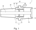
- FIG. 1 shows a longitudinal section view of a bushing 1 according to an embodiment of the present invention.
- the bushing 1 comprises a tubular housing 4, which is formed from two outer shell parts 8, 12.
- both outer shell parts 8, 12 are formed as a truncated cone.
- a first opening 16 is formed from which the housing 4 can be filled with an insulation material.
- a second opening 20 is provided in the second outer shell part 12.
- a flange portion 24 is formed at an axial side of the second outer shell part 12, opposing the axial end of the second outer shell part 12, a flange portion 24 is formed.
- the flange portion 24 is pointing in the direction of the second outer shell part 12. With the flange portion 24 the housing can be mounted to a wall of a switching device.
- the insulation material filled in the housing 4 is omitted.
- an inner surface 32 of the shell parts 8, 12 can be sandblasted or covered with an additional material improving the adhesion.
- a primary conductor 36 is arranged extending between both axial ends of the housing 4. With the primary conductor 36 electric current and voltage is conducted from one to the other axial side.
- measuring equipment 40 is arranged, surrounding the primary conductor 36.
- the measuring equipment 40 comprises a voltage indicator device 44 for detecting whether voltage is present in the primary conductor 36.
- the voltage indicator 44 thereby is formed as a hollow cylinder extending in an axial direction of the primary conductor 36.
- a voltage sensor 48 is provided for measuring the voltage of the primary conductor 36.
- the voltage sensor 48 comprises an electrode element 50 formed as a hollow cylinder and extending in an axial direction of the primary conductor 36.
- the voltage sensor 48 further comprises a shielding electrode 52 surrounding the electrode element 50 and protecting the electrode element 50 against external radiation disturbing the voltage measurement.
- the measuring equipment 40 further comprises a shielded current sensor 56 surrounding the primary conductor 36. With this sensor 56 the current of the primary conductor 36 is measurable.
- FIG. 2 shows an embodiment of a method for manufacturing the bushing 1 according to the present invention.
- the shell parts 8, 12 are produced via a plastic moulding procedure. Both shell parts 8, 12 thereby can be made of the same or a different material.
- the inner surface 32 of the shell parts 8, 12 is treated by sandblasting. Instead of sandblasting the inner surface 32 also can be covered by an additional material improving adhesion of the insulation material.
- the primary conductor 36 is inserted into one of the shell parts 8, 12. After this step, the measuring equipment 40 is assembled D to the at least one shell part 8, 12.
- a next step F an insulation material introducing device (not shown) is connected to the first opening 16, and the housing 4 is filled by the insulation material.
- the remaining air in the housing 4 or in the insulation material is degassed through the second opening 20.
- the bushing 1 is put into a vacuum chamber to generate vacuum condition G to the bushing 1. Under vacuum condition the remaining bubbles in the insulation material can be extracted more easily.
- the insulation material in the housing 4 is cured H. This can be done at ambient temperatures or in an oven. Whether the insulation material is cured in the oven or at ambient temperatures depends which insulation material is used and on the available time for the curing process.
Landscapes
- Engineering & Computer Science (AREA)
- Power Engineering (AREA)
- Insulators (AREA)
Abstract
The present invention relates to a bushing (1) for medium or high voltage switching devices. The bushing (10) comprises a tubular housing (4), wherein a primary conductor (36) for conducting electric current and voltage is provided, axially extending between two axial ends of the housing (4), wherein the housing (4) is filled with an insulation material. The housing (4) is formed from at least two outer shell parts (8, 12) defining a closed internal space (28), comprising at one axial end a first opening (16) for filling the insulation material into the housing (4) and a second opening (20) for degassing the housing (4). A measuring equipment (40) is provided inside the housing (4) surrounding the primary conductor (36).
Description
- The present invention relates to a bushing for medium or high voltage switching devices. The invention further relates to a method for manufacturing a bushing.
- Traditionally, electric power bushings have been made of an electric insulating part formed by a thermosetting resin, such as epoxy, molded around an electrical conductor. The purpose of the insulation has been to prevent electric discharges between the conductor and the wall of a container through which the bushing protrudes. The thermosetting resin has been provided with a sufficiently high thickness to provide a satisfactory functionality in this respect. However, molding thick solid bodies of thermosetting material is a costly process, and alternatives have been searched for.
- Prior art
EP 2 276 041 B1 discloses a device for electric connection to an energy supply conductor for medium or high voltage. The device comprises a housing shell part with a voltage-carrying element, extending in the axial direction of the housing shell. From one opened side of the housing shell part an insulation material is filled inside the housing shell part. In the region where the device is mounting to a wall of a container a shielding element is provided inside the housing shell part surrounding the energy supply conductor for shielding the wall against the electrical field generated by the energy supply conductor. - The problem to be solved by the present invention is to provide a bushing for medium or high voltage switching devices, which can be manufactured more economically, and which has a high functionality.
- The problem is solved by a bushing for medium or high voltage switching devices having the features of
claim 1. Further, the problem is solved by a method for manufacturing such a bushing having the features of claim 10. Preferred embodiments of the invention are specified in the dependent claims. - According to the invention a bushing for medium or high voltage switching devices is proposed. The bushing comprises a tubular housing, wherein a primary conductor for conducting electric current and voltage is provided, axially extending between two axial ends of the housing. The housing is filled with an insulation material. Further, the housing is formed from at least two outer shell parts defining a closed internal space, comprising at one axial end a first opening for filling the insulation material into the housing and a second opening for degassing the housing, wherein a measuring equipment is provided inside the housing surrounding the primary conductor.
- The tubular housing thereby comprises a longitudinal shape. Inside the housing the primary conductor is arranged extending in the direction of the longitudinal housing. For electrically insulating the primary conductor to an external surface of the housing the insulating material is provided between the conductor and the housing. To enable a complete filling of the housing the first and the second opening preferably are provided at an outermost axial end of the housing. Both openings thereby are provided on the same axial end. The size of the openings is dimensioned to just enable the filling and the degassing of the housing. Accordingly, the openings can be provided as e.g. drilling holes. Preferably, after filling the insulation material into the housing the openings can be closed by a cap.
- By providing outer shell parts which are filled with insulation material a perfect surface quality of the bushing can be guaranteed. In contrast to bushings which are molded in an external form, the scrap rate of bushings having an imperfect surface quality can be significantly decreased. The bushings therefore can be produced more economically. Further, by providing measuring equipment inside the housing, no external measuring equipment is necessary, so that the bushing has a high functionality.
- In a preferred embodiment of the invention, the measuring equipment comprises a voltage sensor and/or a current sensor and/or a voltage indicator device. By the usage of a voltage sensor respectively a current sensor the voltage and the current of the primary conductor can be measured. By additionally providing a voltage indicator device it is possible to provide a simple device which in case of failure of the voltage sensor indicates that voltage is present in the primary conductor. The voltage indicator therefore is a safety measure to re-check the results of the voltage sensor and to protect a user. A handling safety of the bushing thereby is increased.
- In a further preferred embodiment, the voltage sensor comprises an electrode element surrounding the primary conductor and a shielding element surrounding the electrode element. In other words, the shielding electrode is provided at an outer circumference of the electrode element. The shielding electrode thereby protects the electrode element from radiation from outside of the bushing. As this radiation would influence the voltage measurement, by providing the shielding electrode the accuracy of the voltage measurement can be improved.
- Preferably, at least one shell part is forming a truncated cone structure. In other words, the diameter of the shell part decreases in the direction of the axial end of the respective shell part. This design has the advantage that the shell parts can be easily manufactured by plastic molding. Further, the risk of remaining bubbles in corner regions is decreased, so that the scrap rate due to electric discharges is reduced. The bushing therefore can be manufactured more economically.
- In a further advantageous development, the shell parts are made of different materials. During use of the bushing, both shell parts are usually provided to different outer conditions. In particular, the second shell part is provided inside a switching device which is filled with an insulation gas like sulfur hexafluoride (SF6). In contrast thereto, the first shell part usually is provided to ambient air. By using different materials for both shell parts these materials can be chosen which suits best for the specific environment. For the second shell part preferably, a material is chosen having a higher resistance to hydrolysis, whereas for the first shell part a material is chosen, which is compatible to environment gas.
- In a preferred embodiment, at least one shell part is made of a thermoplastic or thermoset material. Usage of thermoset material has the advantage that this material has a high heat resistance and a high structural integrity. In particular, thermoset material retains their strength and shape even when heated. Further, this material also has a high dielectric strength and resistance to corrosion effects and water. Apart from this this material also has a low price. In contrast thereto, although the temperature resistance of thermoplastic is lower than for thermoset material, the thermoplastic material has a high electrical insulation and can be remoulded or reshaped. Further, this material also has a low price.
- A preferred embodiment specifies that the insulation material is made, at least partly of a thermoplastic, thermoset or gaseous material. By using such a material, a high insulation resistance can be achieved. In a further preferred embodiment, the insulation material is a silicon-based material. Also, with this material a high insulation resistance can be achieved.
- Preferably, inner surfaces of the shell parts are sandblasted. by providing a sandblasted inner surface of the shell parts adhesion between the insulation material and the inner surface can be improved. By such an inner surface it can be prevented that due to shrinkage during the curing process the insulation material separates from the inner walls. The scrap rate of bushings thereby can be decreased so that the bushing can be manufactured more economically.
- In an advantageous embodiment, inner surfaces of the shell parts are covered by a material improving an adhesion between the filling material and the shell parts. Also, by covering the inner surface with an additional material it can be prevented that the insulation material separates to the inner surface. Accordingly, also with such an inner surface the scrap rate of bushings can be decreased. Therefore, the bushing can be produced more economically.
- The problem is further solved by a method for manufacturing a bushing. The method comprises the steps of producing both shell parts, insertion of the primary conductor into one of the shell parts, assembling the measuring equipment into at least one of the shell parts, and connecting both shell parts to each other. In further steps, the insulation material is filled into the housing through the first opening, and the insulation material is cured in the housing. With these steps, a bushing is achieved having a high surface quality. Further, the scrap rate of such a method is low, so that the bushing can be manufactured more economically. Apart from this, the above-mentioned advantages and effects are achieved.
- In a preferred embodiment, inner surfaces of the shell parts are treated by sandblasting. With this method step the adhesion between the insulation material and the inner surface is improved. Accordingly, with this method step the effect and advantages described above are achieved.
- Advantageously, inner surfaces of the shell parts are covered by a material improving an adhesion between the insulation material and the shell parts. Accordingly, with this method step the effect and advantages described above are achieved.
- In a further advantage embodiment, after filling of the insulation material into the housing a degassing step is performed under vacuum conditions. By conducting the degassing step under vacuum conditions, the bubbles in the insulation material can be extracted more efficiently. Thereby, the insulation between the primary conductor and an outside of the bushing is improved. The scrap rate of bushings due to electric discharges can be significantly reduced. Accordingly, with this method step the bushing can be manufactured more economically.
- The above aspects and examples will become apparent from and be elucidated with reference to the embodiments described hereinafter.
- The subject matter of the Invention will be explained in more details in the following description illustrated in the drawings, in which:
- Figure 1
- Longitudinal section view of a bushing according to an embodiment of the present invention, and
- Figure 2
- Embodiment of the method for manufacturing the bushing according to the present invention.
-
Figure 1 shows a longitudinal section view of abushing 1 according to an embodiment of the present invention. Thebushing 1 comprises atubular housing 4, which is formed from twoouter shell parts outer shell parts outer shell part 12, afirst opening 16 is formed from which thehousing 4 can be filled with an insulation material. Further, at the same axial end, asecond opening 20 is provided in the secondouter shell part 12. At an axial side of the secondouter shell part 12, opposing the axial end of the secondouter shell part 12, aflange portion 24 is formed. Theflange portion 24 is pointing in the direction of the secondouter shell part 12. With theflange portion 24 the housing can be mounted to a wall of a switching device. - In order, to ensure good visibility of the
internal space 28 of thehousing 4, the insulation material filled in thehousing 4 is omitted. To provide a good adhesion between theshell parts inner surface 32 of theshell parts housing 4, aprimary conductor 36 is arranged extending between both axial ends of thehousing 4. With theprimary conductor 36 electric current and voltage is conducted from one to the other axial side. In the middle of thehousing 4measuring equipment 40 is arranged, surrounding theprimary conductor 36. In this embodiment, the measuringequipment 40 comprises avoltage indicator device 44 for detecting whether voltage is present in theprimary conductor 36. Thevoltage indicator 44 thereby is formed as a hollow cylinder extending in an axial direction of theprimary conductor 36. - Close to an end of the
voltage indicator 44, avoltage sensor 48 is provided for measuring the voltage of theprimary conductor 36. Thevoltage sensor 48 comprises anelectrode element 50 formed as a hollow cylinder and extending in an axial direction of theprimary conductor 36. Thevoltage sensor 48 further comprises a shieldingelectrode 52 surrounding theelectrode element 50 and protecting theelectrode element 50 against external radiation disturbing the voltage measurement. The measuringequipment 40 further comprises a shieldedcurrent sensor 56 surrounding theprimary conductor 36. With thissensor 56 the current of theprimary conductor 36 is measurable. -
Figure 2 shows an embodiment of a method for manufacturing thebushing 1 according to the present invention. In a first step A of the method theshell parts shell parts inner surface 32 of theshell parts inner surface 32 also can be covered by an additional material improving adhesion of the insulation material. In a next step C, theprimary conductor 36 is inserted into one of theshell parts equipment 40 is assembled D to the at least oneshell part - After everything is properly arranged in the
shell part shell part shell part shell parts first opening 16, and thehousing 4 is filled by the insulation material. The remaining air in thehousing 4 or in the insulation material is degassed through thesecond opening 20. To reduce remaining bubbles in the insulation material, thebushing 1 is put into a vacuum chamber to generate vacuum condition G to thebushing 1. Under vacuum condition the remaining bubbles in the insulation material can be extracted more easily. After this step, the insulation material in thehousing 4 is cured H. This can be done at ambient temperatures or in an oven. Whether the insulation material is cured in the oven or at ambient temperatures depends which insulation material is used and on the available time for the curing process. -
- 1
- bushing
- 4
- housing
- 8
- first shell part
- 12
- second shell part
- 16
- first opening
- 20
- second opening
- 24
- flange portion
- 28
- Internal space
- 32
- inner surface
- 36
- primary conductor
- 40
- measuring equipment
- 44
- voltage indicator device
- 48
- voltage sensor
- 50
- electrode element
- 52
- shielding electrode
- 56
- current sensor
- A
- step
- B
- step
- C
- step
- D
- step
- E
- step
- F
- step
- G
- step
- H
- step
Claims (13)
- A bushing (1) for medium or high voltage switching devices, comprising a tubular housing (4), wherein a primary conductor (36) for conducting electric current and voltage is provided, axially extending between two axial ends of the housing (4), wherein the housing (4) is filled with an insulation material, characterized in that
the housing (4) is formed from at least two outer shell parts (8, 12) defining a closed internal space (28), comprising at one axial end a first opening (16) for filling the insulation material into the housing (4) and a second opening (20) for degassing the housing (4), wherein a measuring equipment (40) is provided inside the housing (4) surrounding the primary conductor (36). - Bushing (1) according to claim 1, characterized in that the measuring equipment (40) comprises a voltage sensor (48) and/or a current sensor (56) and/or a voltage indicator device (44).
- Bushing (1) according to claim 2, characterized in that the voltage sensor (48) comprises an electrode element (50) surrounding the primary conductor (36) and a shielding element (52) surrounding the electrode element (50).
- Bushing (1) according to one of the preceding claims, characterized in that at least one shell part (8, 12) is forming a truncated cone structure.
- Bushing according to one of the preceding claims, characterized in that the shell parts (8, 12) are made of different materials.
- Bushing (1) according to one of the preceding claims, characterized in that at least one shell part (8, 12) is made of a thermoplastic or thermoset material.
- Bushing (1) according to one of the preceding claims, characterized in that the insulation material is made, at least partly of a thermoplastic, thermoset or gaseous material.
- Bushing (1) according to one of the preceding claims, characterized in that inner surfaces (32) of the shell parts (8, 12) are sandblasted.
- Bushing (1) according to one of the claims 1 to 7, characterized in that inner surfaces (32) of the shell parts (8, 12) are covered by a material improving an adhesion between the insulation material and the shell parts (8, 12).
- Method for manufacturing a bushing (1) according to one of the preceding claims, comprising the steps:- Producing (A) both shell parts (8, 12),- Insertion (C) of the primary conductor (36) into one of the shell parts (8, 12),- Assembling (D) the measuring equipment (40) into at least one of the shell parts (8, 12),- Connecting (E) both shell parts (8, 12) to each other,- Filling (F) the insulation material into the housing (4) through the first opening (16), and- Curing (H) the insulation material in the housing (4).
- Method according to claim 10, characterized in that inner surfaces of the shell parts are treated (B) by sandblasting.
- Method according to claim 10, characterized in that inner surfaces (32) of the shell parts (8, 12) are covered (B) by a material improving an adhesion between the filling material and the shell parts (8, 12).
- Method according to claims 10 to 12, characterized in that after filling of the insulation material into the housing (4) a degassing step (G) is performed under vacuum conditions.
Priority Applications (1)
| Application Number | Priority Date | Filing Date | Title |
|---|---|---|---|
| EP23215294.2A EP4567838A1 (en) | 2023-12-08 | 2023-12-08 | Bushing for medium or high voltage applications and method for manufacturing the bushing |
Applications Claiming Priority (1)
| Application Number | Priority Date | Filing Date | Title |
|---|---|---|---|
| EP23215294.2A EP4567838A1 (en) | 2023-12-08 | 2023-12-08 | Bushing for medium or high voltage applications and method for manufacturing the bushing |
Publications (1)
| Publication Number | Publication Date |
|---|---|
| EP4567838A1 true EP4567838A1 (en) | 2025-06-11 |
Family
ID=89164193
Family Applications (1)
| Application Number | Title | Priority Date | Filing Date |
|---|---|---|---|
| EP23215294.2A Pending EP4567838A1 (en) | 2023-12-08 | 2023-12-08 | Bushing for medium or high voltage applications and method for manufacturing the bushing |
Country Status (1)
| Country | Link |
|---|---|
| EP (1) | EP4567838A1 (en) |
Citations (5)
| Publication number | Priority date | Publication date | Assignee | Title |
|---|---|---|---|---|
| US3009983A (en) * | 1959-09-30 | 1961-11-21 | Gen Electric | Bushing structure for electric apparatus |
| JP2002025371A (en) * | 2000-07-13 | 2002-01-25 | Toshiba Corp | Bushing |
| US20050135028A1 (en) * | 2000-03-01 | 2005-06-23 | Hitachi, Ltd. | Gas insulating apparatus and method for locating fault point thereof |
| US20100258347A1 (en) * | 2007-10-12 | 2010-10-14 | Patrik Roseen | Device for electric connection, a method for producing such a device, and an electric power installation provided therewith |
| EP2276041B1 (en) | 2009-07-15 | 2013-09-25 | ABB Research Ltd. | A device for electric connection and an electric installation |
-
2023
- 2023-12-08 EP EP23215294.2A patent/EP4567838A1/en active Pending
Patent Citations (5)
| Publication number | Priority date | Publication date | Assignee | Title |
|---|---|---|---|---|
| US3009983A (en) * | 1959-09-30 | 1961-11-21 | Gen Electric | Bushing structure for electric apparatus |
| US20050135028A1 (en) * | 2000-03-01 | 2005-06-23 | Hitachi, Ltd. | Gas insulating apparatus and method for locating fault point thereof |
| JP2002025371A (en) * | 2000-07-13 | 2002-01-25 | Toshiba Corp | Bushing |
| US20100258347A1 (en) * | 2007-10-12 | 2010-10-14 | Patrik Roseen | Device for electric connection, a method for producing such a device, and an electric power installation provided therewith |
| EP2276041B1 (en) | 2009-07-15 | 2013-09-25 | ABB Research Ltd. | A device for electric connection and an electric installation |
Similar Documents
| Publication | Publication Date | Title |
|---|---|---|
| CN101443972B (en) | An electric connection device and a electricity station with the electric connection device | |
| CN101874277B (en) | Device for electrical connection, method for producing the device and electric device with the device | |
| US8402636B2 (en) | Method of manufacturing ground-burial type solid insulated transformer | |
| US20100284133A1 (en) | Method Of Producing An Electric Power Device, And An Electric Power Device | |
| CN102568757A (en) | Plug bushings and high-voltage installations with such bushings | |
| CN101326595B (en) | Injection-molded external-cone bushing | |
| EP2168212A2 (en) | An adapter, a cable connector with the adapter and a cable connector assembly | |
| KR910001321B1 (en) | Molded high voltage splice body | |
| US20060011589A1 (en) | Production of a circuit-breaker pole, insulated by a solid material | |
| US20120178294A1 (en) | Device For Electric Connection And An Electric Installation | |
| CN102473489B (en) | For be electrically connected equipment, for the manufacture of the method for this kind equipment and electric device | |
| CN114008883A (en) | Cable accessory | |
| KR20220120695A (en) | Bushing with an electrically conductive head mounted to a condenser core | |
| WO1994029678A1 (en) | Material level probe having crimp seal | |
| CN215342160U (en) | Novel dry-type sleeve for electric power system | |
| US9004929B2 (en) | Manufacturing method for electric component and electrical component | |
| EP1815485B1 (en) | Electrical high voltage generator | |
| US12068089B2 (en) | Dry-type plug-in bushing, manufacturing method of the same, and high-voltage installation comprising same | |
| CN105651414A (en) | Temperature sensor with enhanced tensile strength | |
| FI118168B (en) | Protection against exploding an electrical appliance with a molded shell | |
| CN106356159A (en) | Insulating sleeve for medium-high voltage connection and manufacturing method thereof | |
| JP6570578B2 (en) | Bushing | |
| EP3316273B1 (en) | Pole part for medium voltage switchgear | |
| JP7675590B2 (en) | Cable Termination Connection | |
| RU2201002C2 (en) | High-voltage current transformer |
Legal Events
| Date | Code | Title | Description |
|---|---|---|---|
| PUAI | Public reference made under article 153(3) epc to a published international application that has entered the european phase |
Free format text: ORIGINAL CODE: 0009012 |
|
| STAA | Information on the status of an ep patent application or granted ep patent |
Free format text: STATUS: THE APPLICATION HAS BEEN PUBLISHED |
|
| AK | Designated contracting states |
Kind code of ref document: A1 Designated state(s): AL AT BE BG CH CY CZ DE DK EE ES FI FR GB GR HR HU IE IS IT LI LT LU LV MC ME MK MT NL NO PL PT RO RS SE SI SK SM TR |
|
| STAA | Information on the status of an ep patent application or granted ep patent |
Free format text: STATUS: REQUEST FOR EXAMINATION WAS MADE |
|
| 17P | Request for examination filed |
Effective date: 20251209 |