EP4567756A1 - Fingerprint array structure, fingerprint sensor chip, and electronic device - Google Patents
Fingerprint array structure, fingerprint sensor chip, and electronic device Download PDFInfo
- Publication number
- EP4567756A1 EP4567756A1 EP24201647.5A EP24201647A EP4567756A1 EP 4567756 A1 EP4567756 A1 EP 4567756A1 EP 24201647 A EP24201647 A EP 24201647A EP 4567756 A1 EP4567756 A1 EP 4567756A1
- Authority
- EP
- European Patent Office
- Prior art keywords
- pixel
- array
- fingerprint
- array structure
- circuit
- Prior art date
- Legal status (The legal status is an assumption and is not a legal conclusion. Google has not performed a legal analysis and makes no representation as to the accuracy of the status listed.)
- Pending
Links
Images




Classifications
-
- G—PHYSICS
- G06—COMPUTING OR CALCULATING; COUNTING
- G06V—IMAGE OR VIDEO RECOGNITION OR UNDERSTANDING
- G06V40/00—Recognition of biometric, human-related or animal-related patterns in image or video data
- G06V40/10—Human or animal bodies, e.g. vehicle occupants or pedestrians; Body parts, e.g. hands
- G06V40/12—Fingerprints or palmprints
- G06V40/13—Sensors therefor
- G06V40/1306—Sensors therefor non-optical, e.g. ultrasonic or capacitive sensing
Definitions
- the present application relates to the technical field of fingerprint identification, and in particular to a fingerprint array structure, a fingerprint sensor chip and an electronic device.
- the pixel array proportion of an existing capacitive fingerprint sensor chips is usually between 60% and 75%, especially the pixel array proportion of a small-area capacitive fingerprint sensor chip is lower. Therefore, how to increase the proportion of a pixel array in a chip and reduce the area of a chip is urgent technical problems which need to be solved by those skilled in the art.
- the embodiments of the present application provide a fingerprint array structure, a fingerprint sensor chip, and an electronic device to solve at least some of the above-mentioned technical problems.
- a fingerprint array structure including:
- the pixel array includes a plurality of pixel units arranged in an array, the plurality of pixel units are divided into a plurality of pixel groups, and each pixel group includes at least two pixel units;
- the pixel units located on the same row or the same column of the pixel array constitute one pixel group.
- connecting terminals of the plurality of connecting line groups are positioned on the same end.
- connecting terminals of the plurality of connecting line groups are positioned on the outer side of an area where the pixel array is located.
- projections of the non-pixel circuits and the pixel circuits perpendicularly facing the pixel array are all positioned on the pixel array.
- the fingerprint array structure further includes a shielding layer, and a projection of the shielding layer perpendicularly facing the pixel array at least partially overlaps the projection of the non-pixel circuits perpendicularly facing the pixel array.
- the shielding layer includes power supplies.
- the shielding layer includes ground networks.
- the shielding layer includes power supplies and ground networks, and the power supplies and the ground networks are spaced apart from each other in a long strip shape.
- a fingerprint sensor chip including the above fingerprint array structure.
- the area outside the fingerprint array structure is provided with an IO circuit.
- an electronic device including the above fingerprint sensor chip.
- the area of the fingerprint array structure can be reduced.
- the proportion of the pixel array of the present application is higher and the chip area is smaller on the condition that the size specifications of pixel arrays are the same.
- Pixel array 11. Pixel unit; 2. Connecting line group; 21. Connecting terminal; 22. Connecting line; 3. Shielding layer; 4. Pixel circuit; and 5. Non-pixel circuit.
- the layout of a circuit module of a common capacitive fingerprint sensor chip is shown in FIG. 1 , and the circuit module is composed of a pixel array, a line control circuit module, a column-level readout circuit and a control unit module thereof, other analog circuit modules and digital circuit modules, an IO (Input/Output) circuit module, etc.
- the pixel array is a matrix composed of pixel units in X rows and Y columns, a finger capacitive induction polar plate is called a pixel unit, and generally one pixel unit corresponds to one readout circuit.
- the readout circuit corresponding to the pixel unit and the control circuit of the pixel unit are called pixel circuits, and the remaining circuits are called non-pixel circuit.
- a fingerprint array structure is provided and is particularly applicable to a capacitive fingerprint array.
- the circuit layer and the pixel array are arranged in a partially or fully overlapping manner, so that the area of the capacitive fingerprint sensor chip is reduced.
- the non-pixel circuit can be placed below the pixel array to enable the pixel circuit and the non-pixel circuit to share the area of the pixel array, so that the chip area is greatly reduced, and the proportion of the pixel array is increased.
- the fingerprint array structure provided by the present application includes a pixel array 1, a plurality of connecting line groups 2 and a circuit layer, where the circuit layer includes pixel circuits 4 and non-pixel circuits 5, and at least one portion of the circuit layer overlaps the pixel array 1.
- the pixel array 1 includes a plurality of pixel units 11 arranged in an array, optionally, the plurality of pixel units 11 are distributed in a rectangular array and constitute a pixel group, one pixel group is connected to one pixel circuit 4, that is, a plurality of pixel units 11 in the same pixel group are connected to the same pixel circuit 4.
- a plurality of pixel units 11 on the same row or same column of the pixel array 1 constitute one pixel group.
- a plurality of pixel circuits 4 are arranged, each pixel circuit 4 is connected to one pixel group, and a plurality of pixel units 11 in the same pixel group multiplex one pixel circuit 4 in a time-sharing manner.
- the number of the pixel circuits 4 is small than that of the pixel units 11, so that the area of the pixel circuits 4 can be reduced.
- the pixel circuits 4 and the non-pixel circuits 5 are positioned on the same layer, in addition, projections of the non-pixel circuits 5 and the pixel circuits 4 perpendicularly facing the pixel array 1 are all positioned on the pixel array 1, that is, the areas of the projections of the non-pixel circuits 5 and the pixel circuits 4 perpendicularly facing the pixel array 1 are less than or equal to the area of the pixel array 1, and the proportion of the pixel array 1 can be increased, so that the performance of a small-area chip can be improved.
- the pixel groups and the pixel circuits 4 are electrically connected through the connecting line groups 2, each pixel circuit 4 corresponds to one connecting line group 2, each connecting line group 2 includes a plurality of connecting lines 22, each connecting line 22 is connected to one pixel unit 11, and a plurality of connecting lines 22 are connected to the pixel circuits 4 through the connecting terminals.
- connecting terminals 21 of the plurality of connecting line groups 2 are positioned on the same end of the connecting line groups 2, so that the pixel circuits 4 are positioned on the same end of the pixel array 1 to provide a more regular area to arrange the non-pixel circuits 5, that is, the non-pixel circuits 5 can be arranged in the same area.
- connecting terminals 21 of the plurality of connecting line groups 2 are positioned on the outer side of an area where the pixel array 1 is located to ensure consistency of the pixel array 1, for example, to ensure the thickness of the pixel array, and the consistency of the pixel units 11 with stray capacitance of metals around, so that local thickness of the pixel array 1 and the stray capacitance are prevented from being non-uniform due to arrangement of the connecting terminals 21.
- the connecting terminals 21 can be arranged at any positions, which will not affect the function of the array structure and will only cause certain difference on the consistency of the array structure.
- the shielding layer 3 is further included and is at least arranged between the non-pixel circuits 5 and the connecting line groups 2, and in addition, the projection of the shielding layer 3 perpendicularly facing the pixel array 1 at least overlaps the projection of the non-pixel circuits 5, that is, the shielding layer 3 at least isolates the non-pixel circuits 5.
- the function of the shielding layer 3 is to isolate the pixel units 11 and the connecting line groups 2 from the area of the non-pixel circuits 5, so that the non-pixel circuits 5 can be prevented from interfering with normal operation of the pixel units 11 above the non-pixel circuits 5 to avoid louder noise and larger interference.
- areas of the non-pixel circuits 5 and pixel circuits 4 are provided with the shielding layers 3, so that the shielding layers 3 can form a complete layer to ensure thickness consistency of the array structure and enable the non-pixel circuits 5 and pixel circuits 4 to be on the same layer.
- the shielding layer 3 includes power supplies or ground networks, and a magnetic field can be formed through the power supplies or the ground networks, so that the non-pixel circuits 5 can be prevented from interfering with normal operation of the pixel units 11 above the non-pixel circuits 5 to avoid louder noise and larger interference.
- the power supply includes a source terminal of each circuit or element in the fingerprint array structure, the ground network is composed of a ground wire or a zero line of each circuit and element.
- the shielding layer 3 includes power supplies and ground networks, the power supplies and ground networks are of strip-shaped structures and are spaced apart from each other at equal intervals, the array structure and all power supplies and ground networks of the chip are distributed at equal intervals to form the shielding layer 3, in this way, the shielding layer 3 can also serve as the power supplies and ground networks of the pixel circuits 4 and the non-pixel circuits 5, so that resources and the using layers of metal layers can be saved, and optionally, the power supplies and ground networks are spaced apart from each other.
- the embodiments of the present application solve the technical problem in the prior art that the non-pixel circuits 5 occupy a larger chip area to reduce the proportion of the pixel array 1.
- the proportion of the pixel array 1 of a capacitive fingerprint sensor chip can be increased to above 90%, and in a pixel array 1 of a chip with a larger area, the proportion of the pixel array 1 can even be close to 98%.
- the proportion of the pixel array disclosed in the present application is the highest, the chip area is the smallest, and the cost is the lowest.
- each pixel unit 11 is composed of top-layer metal polar plates, and a plurality of substrates on the same row constitute one pixel group.
- Lower-layer metal of the top-layer metal polar plates constitute a connecting line group 2
- connecting terminals 21 of the connecting line group 2 are positioned at the tail end of the connecting line group 2 (the left side as shown in FIGs. 2 and 3 , and in other embodiments, also can be arranged on the right side), so that a plurality of pixel units 11 on the same row can multiplex the same pixel circuit 4 in a time-sharing manner to output pixel signals.
- the shielding layer 3 is formed on the lower layer of the connecting line group 2 to isolate the pixel units 11 and the connecting line group 2 from the area of the non-pixel circuits, so that the non-pixel circuits 5 can be prevented from interfering with normal operation of the pixel units 11 above the non-pixel circuits 5 to avoid louder noise and larger interference.
- a projection drawing of the shielding layer 3 overlaps that of an area in which the pixel circuits 4 and the non-pixel circuits 5 are positioned.
- the pixel circuits 4 and the non-pixel circuits 5 are arranged on the lower layer of the shielding layer 3, where the pixel circuits 4 are arranged close to the left side, that is arranged close to connecting terminals 21 of the connecting line group 2.
- the pixel circuits 4 occupy an area corresponding to first to third columns of pixel units 11, and the area corresponding to other columns of pixel units 11 are configured to arrange the non-pixel circuits 5.
- the pixel units 11 on the same row or same column of the fingerprint array structure provided by the embodiments of the present application share the pixel circuits 4, a larger area on the lower side of the pixel array 1 can be reserved to arrange the non-pixel circuits 5, and the shielding layer 3 is also arranged to isolate the pixel units 11 and the connecting line groups 2 from the non-pixel circuits 5, so that the non-pixel circuits 5 can be prevented from interfering with normal operation of the pixel units 11 above the non-pixel circuits 5 to avoid louder noise and larger interference.
- a fingerprint sensor chip is provided, as shown in FIG. 5 , the fingerprint sensor chip includes the fingerprint array structure, as shown in FIG. 5 , only an IO circuit and necessary spaces specified by the process are arranged at the area outside the fingerprint array structure, so that the chip can have a higher proportion of the pixel array 1.
- an electronic device including the fingerprint sensor chip.
- the electronic device includes a smartphone, a tablet computer, a laptop, and a fingerprint lock with a fingerprint identification function.
- connection may be a fixed connection, a detachable connection, or an integrated connection, may be a mechanical connection or an electrical connection, may be a direct connection or an indirect connection by means of an intermediate medium, or may be an internal connection of two elements or an interaction between two elements, unless otherwise clearly defined.
- connection may be a fixed connection, a detachable connection, or an integrated connection, may be a mechanical connection or an electrical connection, may be a direct connection or an indirect connection by means of an intermediate medium, or may be an internal connection of two elements or an interaction between two elements, unless otherwise clearly defined.
- connection may be a fixed connection, a detachable connection, or an integrated connection, may be a mechanical connection or an electrical connection, may be a direct connection or an indirect connection by means of an intermediate medium, or may be an internal connection of two elements or an interaction between two elements, unless otherwise clearly defined.
- specific meaning of the terms in the present application may be understood according to specific situations.
- references to the embodiment, “one embodiment”, “some embodiments”, “example”, “specific example”, or “some examples”, etc. mean that specific features, structures, materials, or characteristics described in connection with the embodiment or example are included in at least one embodiment or example of the present application.
- schematic expressions of the above terms need not be directed to the same embodiment or example.
- the described specific feature, structure, material, or characteristic can be combined in any suitable way in one or more embodiments or examples.
- different embodiments or examples described in this specification and features of different embodiments or examples may be combined by those skilled in the art without contradicting one another.
- first and second are merely used for description purposes and cannot be interpreted as indicating or implying relative importance or implicitly indicating the number of technical features indicated. Therefore, the features defined with “first” and “second” can explicitly or implicitly include one or more features.
- a plurality of means at least two, e.g., two, three, etc., unless otherwise specified.
Landscapes
- Engineering & Computer Science (AREA)
- Human Computer Interaction (AREA)
- Physics & Mathematics (AREA)
- General Physics & Mathematics (AREA)
- Multimedia (AREA)
- Theoretical Computer Science (AREA)
- Image Input (AREA)
Abstract
Description
- The present application relates to the technical field of fingerprint identification, and in particular to a fingerprint array structure, a fingerprint sensor chip and an electronic device.
- Sensor chips are mostly composed of pixel arrays and various circuit modules, and the proportion of a pixel array is one of the key competitiveness of sensor chips, and is defined as: proportion of a pixel array=pixel array area ÷ chip area. The pixel array proportion of an existing capacitive fingerprint sensor chips is usually between 60% and 75%, especially the pixel array proportion of a small-area capacitive fingerprint sensor chip is lower. Therefore, how to increase the proportion of a pixel array in a chip and reduce the area of a chip is urgent technical problems which need to be solved by those skilled in the art.
- Aiming at the shortcomings in the prior art, the embodiments of the present application provide a fingerprint array structure, a fingerprint sensor chip, and an electronic device to solve at least some of the above-mentioned technical problems.
- In order to realize the above-mentioned technical purposes, according to a first aspect of the embodiments of the present application, there is provided a fingerprint array structure, including:
- a pixel array, where the pixel array includes a plurality of pixel units arranged in an array, the plurality of pixel units are divided into a plurality of pixel groups, and each pixel group includes at least two pixel units;
- a circuit layer, where the circuit layer includes a plurality of pixel circuits and a plurality of non-pixel circuits, and at least one portion of a projection of the circuit layer perpendicularly facing the pixel array overlaps the pixel array;
- a plurality of connecting line groups, where each connecting line group includes a plurality of connecting lines, each connecting line is connected to one pixel unit, and each pixel circuit is electrically connected to a plurality of pixel units of one pixel group through one connecting line group.
- Further, the pixel units located on the same row or the same column of the pixel array constitute one pixel group.
- Further, connecting terminals of the plurality of connecting line groups are positioned on the same end.
- Further, connecting terminals of the plurality of connecting line groups are positioned on the outer side of an area where the pixel array is located.
- Further, projections of the non-pixel circuits and the pixel circuits perpendicularly facing the pixel array are all positioned on the pixel array.
- Further, the fingerprint array structure further includes a shielding layer, and a projection of the shielding layer perpendicularly facing the pixel array at least partially overlaps the projection of the non-pixel circuits perpendicularly facing the pixel array.
- Further, the shielding layer includes power supplies.
- Further, the shielding layer includes ground networks.
- Further, the shielding layer includes power supplies and ground networks, and the power supplies and the ground networks are spaced apart from each other in a long strip shape.
- According to a second aspect of the embodiments of the present application, there is provided a fingerprint sensor chip, including the above fingerprint array structure.
- Further, the area outside the fingerprint array structure is provided with an IO circuit.
- According to a third aspect of the embodiments of the present application, there is provided an electronic device, including the above fingerprint sensor chip.
- The beneficial effects of the embodiments of the present application are as follows:
- According to the embodiments of the present application, through arranging at least portion of the circuit layer and the pixel array in an overlapping manner, the area of the fingerprint array structure can be reduced. When the fingerprint array structure is applied to a chip, the proportion of the pixel array of the present application is higher and the chip area is smaller on the condition that the size specifications of pixel arrays are the same.
-
-
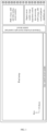
FIG. 1 is a schematic structural diagram of the layout of a circuit module of a capacitive fingerprint sensor chip in the prior art; -
FIG. 2 is a schematic structural diagram of an cross section of a fingerprint array structure according to one embodiment of the present application; -
FIG. 3 is a schematic structural diagram of an cross section of a fingerprint array structure according to one embodiment of the present application; -
FIG. 4 is a schematic structural diagram of a top view of a fingerprint array structure according to one embodiment of the present application; - and
FIG. 5 is a schematic structural diagram of a fingerprint sensor chip framework according to one embodiment of the present application. - 1. Pixel array; 11. Pixel unit; 2. Connecting line group; 21. Connecting terminal; 22. Connecting line; 3. Shielding layer; 4. Pixel circuit; and 5. Non-pixel circuit.
- By combining the drawings of the description, the fingerprint array structure and the fingerprint sensor chip provided in the present application will be explained and demonstrated in detail below.
- The layout of a circuit module of a common capacitive fingerprint sensor chip is shown in
FIG. 1 , and the circuit module is composed of a pixel array, a line control circuit module, a column-level readout circuit and a control unit module thereof, other analog circuit modules and digital circuit modules, an IO (Input/Output) circuit module, etc. The pixel array is a matrix composed of pixel units in X rows and Y columns, a finger capacitive induction polar plate is called a pixel unit, and generally one pixel unit corresponds to one readout circuit. The readout circuit corresponding to the pixel unit and the control circuit of the pixel unit are called pixel circuits, and the remaining circuits are called non-pixel circuit. As shown inFIG. 1 , the non-pixel circuit module is distributed outside the array in the prior art, and the proportion of a pixel array=pixel array area ÷ chip area. Therefore, the layout in the prior art enables the proportion of the pixel array to be lower. - According to a first aspect of the embodiments of the present application, a fingerprint array structure is provided and is particularly applicable to a capacitive fingerprint array. According to the embodiments of the present application, the circuit layer and the pixel array are arranged in a partially or fully overlapping manner, so that the area of the capacitive fingerprint sensor chip is reduced. According to the fingerprint array structure, the non-pixel circuit can be placed below the pixel array to enable the pixel circuit and the non-pixel circuit to share the area of the pixel array, so that the chip area is greatly reduced, and the proportion of the pixel array is increased.
- In some embodiments, as shown in
FIGs. 2 and3 , the fingerprint array structure provided by the present application includes apixel array 1, a plurality ofconnecting line groups 2 and a circuit layer, where the circuit layer includespixel circuits 4 andnon-pixel circuits 5, and at least one portion of the circuit layer overlaps thepixel array 1. Thepixel array 1 includes a plurality ofpixel units 11 arranged in an array, optionally, the plurality ofpixel units 11 are distributed in a rectangular array and constitute a pixel group, one pixel group is connected to onepixel circuit 4, that is, a plurality ofpixel units 11 in the same pixel group are connected to thesame pixel circuit 4. Optionally, in the embodiment, a plurality ofpixel units 11 on the same row or same column of thepixel array 1 constitute one pixel group. - A plurality of
pixel circuits 4 are arranged, eachpixel circuit 4 is connected to one pixel group, and a plurality ofpixel units 11 in the same pixel group multiplex onepixel circuit 4 in a time-sharing manner. The number of thepixel circuits 4 is small than that of thepixel units 11, so that the area of thepixel circuits 4 can be reduced. In the embodiment, thepixel circuits 4 and thenon-pixel circuits 5 are positioned on the same layer, in addition, projections of thenon-pixel circuits 5 and thepixel circuits 4 perpendicularly facing thepixel array 1 are all positioned on thepixel array 1, that is, the areas of the projections of thenon-pixel circuits 5 and thepixel circuits 4 perpendicularly facing thepixel array 1 are less than or equal to the area of thepixel array 1, and the proportion of thepixel array 1 can be increased, so that the performance of a small-area chip can be improved. - In some embodiments, the pixel groups and the
pixel circuits 4 are electrically connected through theconnecting line groups 2, eachpixel circuit 4 corresponds to oneconnecting line group 2, each connectingline group 2 includes a plurality of connectinglines 22, each connectingline 22 is connected to onepixel unit 11, and a plurality of connectinglines 22 are connected to thepixel circuits 4 through the connecting terminals. - Optionally, connecting
terminals 21 of the plurality of connectingline groups 2 are positioned on the same end of theconnecting line groups 2, so that thepixel circuits 4 are positioned on the same end of thepixel array 1 to provide a more regular area to arrange thenon-pixel circuits 5, that is, thenon-pixel circuits 5 can be arranged in the same area. - In the embodiment, connecting
terminals 21 of the plurality of connectingline groups 2 are positioned on the outer side of an area where thepixel array 1 is located to ensure consistency of thepixel array 1, for example, to ensure the thickness of the pixel array, and the consistency of thepixel units 11 with stray capacitance of metals around, so that local thickness of thepixel array 1 and the stray capacitance are prevented from being non-uniform due to arrangement of the connectingterminals 21. Only an exemplary introduction to the arrangement manner of the connectingterminals 21 is given in the embodiment. In other embodiments, the connectingterminals 21 can be arranged at any positions, which will not affect the function of the array structure and will only cause certain difference on the consistency of the array structure. - In some embodiments, the
shielding layer 3 is further included and is at least arranged between thenon-pixel circuits 5 and theconnecting line groups 2, and in addition, the projection of theshielding layer 3 perpendicularly facing thepixel array 1 at least overlaps the projection of thenon-pixel circuits 5, that is, theshielding layer 3 at least isolates thenon-pixel circuits 5. The function of theshielding layer 3 is to isolate thepixel units 11 and theconnecting line groups 2 from the area of thenon-pixel circuits 5, so that thenon-pixel circuits 5 can be prevented from interfering with normal operation of thepixel units 11 above thenon-pixel circuits 5 to avoid louder noise and larger interference. - Optionally, areas of the
non-pixel circuits 5 andpixel circuits 4 are provided with the shielding layers 3, so that the shielding layers 3 can form a complete layer to ensure thickness consistency of the array structure and enable thenon-pixel circuits 5 andpixel circuits 4 to be on the same layer. - In some embodiments, the
shielding layer 3 includes power supplies or ground networks, and a magnetic field can be formed through the power supplies or the ground networks, so that thenon-pixel circuits 5 can be prevented from interfering with normal operation of thepixel units 11 above thenon-pixel circuits 5 to avoid louder noise and larger interference. The power supply includes a source terminal of each circuit or element in the fingerprint array structure, the ground network is composed of a ground wire or a zero line of each circuit and element. Or in other embodiments, theshielding layer 3 includes power supplies and ground networks, the power supplies and ground networks are of strip-shaped structures and are spaced apart from each other at equal intervals, the array structure and all power supplies and ground networks of the chip are distributed at equal intervals to form theshielding layer 3, in this way, theshielding layer 3 can also serve as the power supplies and ground networks of thepixel circuits 4 and thenon-pixel circuits 5, so that resources and the using layers of metal layers can be saved, and optionally, the power supplies and ground networks are spaced apart from each other. - The embodiments of the present application solve the technical problem in the prior art that the
non-pixel circuits 5 occupy a larger chip area to reduce the proportion of thepixel array 1. Through arranging thenon-pixel circuits 5 and thepixel array 1 in a stacked manner, the proportion of thepixel array 1 of a capacitive fingerprint sensor chip can be increased to above 90%, and in apixel array 1 of a chip with a larger area, the proportion of thepixel array 1 can even be close to 98%. Compared with the prior art, on the condition that the size specifications of the arrays are the same, the proportion of the pixel array disclosed in the present application is the highest, the chip area is the smallest, and the cost is the lowest. - In one embodiment, as shown in
FIGs. 2 and3 , take thepixel units 11 on the same row constituting a pixel group as an example, eachpixel unit 11 is composed of top-layer metal polar plates, and a plurality of substrates on the same row constitute one pixel group. Lower-layer metal of the top-layer metal polar plates constitute a connectingline group 2, and in the embodiment, connectingterminals 21 of the connectingline group 2 are positioned at the tail end of the connecting line group 2 (the left side as shown inFIGs. 2 and3 , and in other embodiments, also can be arranged on the right side), so that a plurality ofpixel units 11 on the same row can multiplex thesame pixel circuit 4 in a time-sharing manner to output pixel signals. Theshielding layer 3 is formed on the lower layer of the connectingline group 2 to isolate thepixel units 11 and the connectingline group 2 from the area of the non-pixel circuits, so that thenon-pixel circuits 5 can be prevented from interfering with normal operation of thepixel units 11 above thenon-pixel circuits 5 to avoid louder noise and larger interference. In the embodiment, as shown inFIG. 4 , a projection drawing of theshielding layer 3 overlaps that of an area in which thepixel circuits 4 and thenon-pixel circuits 5 are positioned. - The
pixel circuits 4 and thenon-pixel circuits 5 are arranged on the lower layer of theshielding layer 3, where thepixel circuits 4 are arranged close to the left side, that is arranged close to connectingterminals 21 of the connectingline group 2. In the embodiment, thepixel circuits 4 occupy an area corresponding to first to third columns ofpixel units 11, and the area corresponding to other columns ofpixel units 11 are configured to arrange thenon-pixel circuits 5. - The
pixel units 11 on the same row or same column of the fingerprint array structure provided by the embodiments of the present application share thepixel circuits 4, a larger area on the lower side of thepixel array 1 can be reserved to arrange thenon-pixel circuits 5, and theshielding layer 3 is also arranged to isolate thepixel units 11 and the connectingline groups 2 from thenon-pixel circuits 5, so that thenon-pixel circuits 5 can be prevented from interfering with normal operation of thepixel units 11 above thenon-pixel circuits 5 to avoid louder noise and larger interference. - According to a second aspect of the embodiments of the present application, a fingerprint sensor chip is provided, as shown in
FIG. 5 , the fingerprint sensor chip includes the fingerprint array structure, as shown inFIG. 5 , only an IO circuit and necessary spaces specified by the process are arranged at the area outside the fingerprint array structure, so that the chip can have a higher proportion of thepixel array 1. - According to a third aspect of the embodiments of the present application, an electronic device is provided, including the fingerprint sensor chip. Optionally, the electronic device includes a smartphone, a tablet computer, a laptop, and a fingerprint lock with a fingerprint identification function.
- In the description of the present application, it needs to be noted that, orientations or positional relationships indicated by the terms "center", "longitudinal", "transversal", "length", "width", "thickness", "upper", "lower", "front", "rear", "left", "right", "vertical", "horizontal", "top", "bottom", "inner", "outer", "clockwise", "counterclockwise", "axial", "radial", "circumferential", etc. are based on orientations or positional relationships shown in the drawings, and are only for the convenience of describing the present application and simplifying the description, rather than indicating or implying that the apparatus or element referred to must have a specific orientation, be constructed and operated in a specific orientation, and therefore cannot be understood as a limitation on the present application.
- In the present application, unless otherwise clearly specified and limited, the terms "installed", "connected", "connection", "fixed", etc. should be understood broadly. For example, the "connection" may be a fixed connection, a detachable connection, or an integrated connection, may be a mechanical connection or an electrical connection, may be a direct connection or an indirect connection by means of an intermediate medium, or may be an internal connection of two elements or an interaction between two elements, unless otherwise clearly defined. For those of ordinary skill in the art, the specific meaning of the terms in the present application may be understood according to specific situations.
- In the description of this specification, descriptions of the reference terms "the embodiment", "one embodiment", "some embodiments", "example", "specific example", or "some examples", etc. mean that specific features, structures, materials, or characteristics described in connection with the embodiment or example are included in at least one embodiment or example of the present application. In this specification, schematic expressions of the above terms need not be directed to the same embodiment or example. Moreover, the described specific feature, structure, material, or characteristic can be combined in any suitable way in one or more embodiments or examples. In addition, different embodiments or examples described in this specification and features of different embodiments or examples may be combined by those skilled in the art without contradicting one another.
- In addition, the terms "first" and "second" are merely used for description purposes and cannot be interpreted as indicating or implying relative importance or implicitly indicating the number of technical features indicated. Therefore, the features defined with "first" and "second" can explicitly or implicitly include one or more features. In the description of the present application, "a plurality of" means at least two, e.g., two, three, etc., unless otherwise specified.
- The above descriptions are only preferred embodiments of the present application, and are not intended to limit the present application. Any modifications, equivalent replacements, simple improvements etc. made within the substantive content of the present application shall be included in the protection scope of the present application.
Claims (12)
- A fingerprint array structure, comprising:a pixel array, wherein the pixel array comprises a plurality of pixel units arranged in an array, the plurality of pixel units are divided into a plurality of pixel groups, and each pixel group comprises at least two pixel units;a circuit layer, wherein the circuit layer comprises a plurality of pixel circuits and a plurality of non-pixel circuits, and at least one portion of a projection of the circuit layer perpendicularly facing the pixel array overlaps the pixel array;a plurality of connecting line groups, wherein each connecting line group comprises a plurality of connecting lines, each connecting line is connected to one pixel unit, and each pixel circuit is electrically connected to a plurality of pixel units of one pixel group through one connecting line group.
- The fingerprint array structure according to claim 1, characterized in that the pixel units located on the same row or the same column of the pixel array constitute one pixel group.
- The fingerprint array structure according to claim 1, characterized in that connecting terminals of the plurality of connecting line groups are positioned on the same end.
- The fingerprint array structure according to claim 3, characterized in that connecting terminals of the plurality of connecting line groups are positioned on the outer side of an area where the pixel array is located.
- The fingerprint array structure according to claim 1, characterized in that projections of the non-pixel circuit and the pixel circuit perpendicularly facing the pixel array are all positioned on the pixel array.
- The fingerprint array structure according to claim 5, characterized in that the fingerprint array structure further comprises a shielding layer, and a projection of the shielding layer perpendicularly facing the pixel array at least partially overlaps the projection of the non-pixel circuit perpendicularly facing the pixel array.
- The fingerprint array structure according to claim 6, characterized in that the shielding layer comprises power supplies.
- The fingerprint array structure according to claim 6, characterized in that the shielding layer comprises ground networks.
- The fingerprint array structure according to claim 6, characterized in that the shielding layer comprises power supplies and ground networks, and the power supplies and the ground networks are spaced apart from each other in a long strip shape.
- A fingerprint sensor chip, comprising the fingerprint array structure according to any one of claims 1-9.
- The fingerprint sensor chip according to claim 10, characterized in that the area outside the fingerprint array structure is provided with an IO circuit.
- An electronic device, comprising the fingerprint sensor chip according to claim 10 or claim 11.
Applications Claiming Priority (1)
| Application Number | Priority Date | Filing Date | Title |
|---|---|---|---|
| CN202311682858.6A CN117765577A (en) | 2023-12-08 | 2023-12-08 | Fingerprint array structure, fingerprint sensor chip and electronic equipment |
Publications (1)
| Publication Number | Publication Date |
|---|---|
| EP4567756A1 true EP4567756A1 (en) | 2025-06-11 |
Family
ID=90315495
Family Applications (1)
| Application Number | Title | Priority Date | Filing Date |
|---|---|---|---|
| EP24201647.5A Pending EP4567756A1 (en) | 2023-12-08 | 2024-09-20 | Fingerprint array structure, fingerprint sensor chip, and electronic device |
Country Status (4)
| Country | Link |
|---|---|
| US (1) | US12586406B2 (en) |
| EP (1) | EP4567756A1 (en) |
| KR (1) | KR20250088340A (en) |
| CN (1) | CN117765577A (en) |
Citations (1)
| Publication number | Priority date | Publication date | Assignee | Title |
|---|---|---|---|---|
| US9058511B2 (en) * | 2012-11-21 | 2015-06-16 | J-Metrics Technology Co., Ltd. | Biometrics sensor module, assembly, manufacturing method and electronic apparatus using such biometrics sensor module |
Family Cites Families (3)
| Publication number | Priority date | Publication date | Assignee | Title |
|---|---|---|---|---|
| TWI563253B (en) * | 2015-04-14 | 2016-12-21 | Lee Mei Yen | Composite substrate sensor device and method of manufacturing such sensor device |
| JP7245638B2 (en) * | 2018-11-30 | 2023-03-24 | 株式会社ジャパンディスプレイ | detector |
| CN113064513B (en) * | 2021-03-12 | 2023-07-04 | 武汉华星光电半导体显示技术有限公司 | Touch panel and display device |
-
2023
- 2023-12-08 CN CN202311682858.6A patent/CN117765577A/en active Pending
-
2024
- 2024-09-04 US US18/824,471 patent/US12586406B2/en active Active
- 2024-09-05 KR KR1020240120762A patent/KR20250088340A/en active Pending
- 2024-09-20 EP EP24201647.5A patent/EP4567756A1/en active Pending
Patent Citations (1)
| Publication number | Priority date | Publication date | Assignee | Title |
|---|---|---|---|---|
| US9058511B2 (en) * | 2012-11-21 | 2015-06-16 | J-Metrics Technology Co., Ltd. | Biometrics sensor module, assembly, manufacturing method and electronic apparatus using such biometrics sensor module |
Also Published As
| Publication number | Publication date |
|---|---|
| US20250191401A1 (en) | 2025-06-12 |
| CN117765577A (en) | 2024-03-26 |
| KR20250088340A (en) | 2025-06-17 |
| US12586406B2 (en) | 2026-03-24 |
Similar Documents
| Publication | Publication Date | Title |
|---|---|---|
| US20220246093A1 (en) | Display panel and display device | |
| US7974062B2 (en) | Internally overlapped conditioners | |
| CN113554969B (en) | Display panel and display device | |
| US12057382B2 (en) | Chip on film assembly, display panel, and display module | |
| CN109037211B (en) | Capacitor array structure | |
| CN117976649A (en) | LPDDR chip packaging structure and electronic devices | |
| US12586406B2 (en) | Fingerprint array structure, fingerprint sensor chip, and electronic device | |
| US20260073850A1 (en) | Display panel and display device | |
| US12429736B2 (en) | Display substrate and display device | |
| US20250107357A1 (en) | Oled display panels and terminal devices | |
| CN219392640U (en) | Touch panel and display device | |
| US20240081109A1 (en) | Display panel and display apparatus | |
| CN216291563U (en) | Flexible circuit board and electronic equipment thereof | |
| US11360595B2 (en) | Touch display device | |
| US20240381690A1 (en) | Display substrate and display device | |
| CN118198041A (en) | A multilayer metal-oxide-metal capacitor and array thereof | |
| CN216291564U (en) | Flexible circuit board and electronic equipment thereof | |
| CN114005862B (en) | Array substrate, display panel and display device | |
| CN111474782B (en) | Display panel and electronic device | |
| US7394026B2 (en) | Multilayer wiring board | |
| TWI768889B (en) | Cross-type semiconductor capacitor array layout | |
| CN215869365U (en) | Display panel | |
| US12484405B2 (en) | Profiled display panel and display device | |
| US11837597B2 (en) | Semiconductor capacitor array layout with dummy capacitor structure | |
| US12124139B2 (en) | Display substrate and display device |
Legal Events
| Date | Code | Title | Description |
|---|---|---|---|
| PUAI | Public reference made under article 153(3) epc to a published international application that has entered the european phase |
Free format text: ORIGINAL CODE: 0009012 |
|
| STAA | Information on the status of an ep patent application or granted ep patent |
Free format text: STATUS: THE APPLICATION HAS BEEN PUBLISHED |
|
| AK | Designated contracting states |
Kind code of ref document: A1 Designated state(s): AL AT BE BG CH CY CZ DE DK EE ES FI FR GB GR HR HU IE IS IT LI LT LU LV MC ME MK MT NL NO PL PT RO RS SE SI SK SM TR |
|
| STAA | Information on the status of an ep patent application or granted ep patent |
Free format text: STATUS: REQUEST FOR EXAMINATION WAS MADE |
|
| 17P | Request for examination filed |
Effective date: 20251121 |
|
| STAA | Information on the status of an ep patent application or granted ep patent |
Free format text: STATUS: EXAMINATION IS IN PROGRESS |
|
| 17Q | First examination report despatched |
Effective date: 20260120 |