EP4567663A1 - Antenna tuning circuit for an rfid transponder - Google Patents
Antenna tuning circuit for an rfid transponder Download PDFInfo
- Publication number
- EP4567663A1 EP4567663A1 EP24217811.9A EP24217811A EP4567663A1 EP 4567663 A1 EP4567663 A1 EP 4567663A1 EP 24217811 A EP24217811 A EP 24217811A EP 4567663 A1 EP4567663 A1 EP 4567663A1
- Authority
- EP
- European Patent Office
- Prior art keywords
- signal
- operational amplifier
- voltage
- antenna
- control signal
- Prior art date
- Legal status (The legal status is an assumption and is not a legal conclusion. Google has not performed a legal analysis and makes no representation as to the accuracy of the status listed.)
- Pending
Links
Images


Classifications
-
- G—PHYSICS
- G06—COMPUTING OR CALCULATING; COUNTING
- G06K—GRAPHICAL DATA READING; PRESENTATION OF DATA; RECORD CARRIERS; HANDLING RECORD CARRIERS
- G06K19/00—Record carriers for use with machines and with at least a part designed to carry digital markings
- G06K19/06—Record carriers for use with machines and with at least a part designed to carry digital markings characterised by the kind of the digital marking, e.g. shape, nature, code
- G06K19/067—Record carriers with conductive marks, printed circuits or semiconductor circuit elements, e.g. credit or identity cards also with resonating or responding marks without active components
- G06K19/07—Record carriers with conductive marks, printed circuits or semiconductor circuit elements, e.g. credit or identity cards also with resonating or responding marks without active components with integrated circuit chips
- G06K19/0723—Record carriers with conductive marks, printed circuits or semiconductor circuit elements, e.g. credit or identity cards also with resonating or responding marks without active components with integrated circuit chips the record carrier comprising an arrangement for non-contact communication, e.g. wireless communication circuits on transponder cards, non-contact smart cards or RFIDs
- G06K19/0726—Record carriers with conductive marks, printed circuits or semiconductor circuit elements, e.g. credit or identity cards also with resonating or responding marks without active components with integrated circuit chips the record carrier comprising an arrangement for non-contact communication, e.g. wireless communication circuits on transponder cards, non-contact smart cards or RFIDs the arrangement including a circuit for tuning the resonance frequency of an antenna on the record carrier
-
- H—ELECTRICITY
- H03—ELECTRONIC CIRCUITRY
- H03F—AMPLIFIERS
- H03F1/00—Details of amplifiers with only discharge tubes, only semiconductor devices or only unspecified devices as amplifying elements
- H03F1/02—Modifications of amplifiers to raise the efficiency, e.g. gliding Class A stages, use of an auxiliary oscillation
- H03F1/0205—Modifications of amplifiers to raise the efficiency, e.g. gliding Class A stages, use of an auxiliary oscillation in transistor amplifiers
- H03F1/0211—Modifications of amplifiers to raise the efficiency, e.g. gliding Class A stages, use of an auxiliary oscillation in transistor amplifiers with control of the supply voltage or current
- H03F1/0216—Continuous control
-
- G—PHYSICS
- G06—COMPUTING OR CALCULATING; COUNTING
- G06K—GRAPHICAL DATA READING; PRESENTATION OF DATA; RECORD CARRIERS; HANDLING RECORD CARRIERS
- G06K7/00—Methods or arrangements for sensing record carriers, e.g. for reading patterns
- G06K7/10—Methods or arrangements for sensing record carriers, e.g. for reading patterns by electromagnetic radiation, e.g. optical sensing; by corpuscular radiation
- G06K7/10009—Methods or arrangements for sensing record carriers, e.g. for reading patterns by electromagnetic radiation, e.g. optical sensing; by corpuscular radiation sensing by radiation using wavelengths larger than 0.1 mm, e.g. radio-waves or microwaves
- G06K7/10316—Methods or arrangements for sensing record carriers, e.g. for reading patterns by electromagnetic radiation, e.g. optical sensing; by corpuscular radiation sensing by radiation using wavelengths larger than 0.1 mm, e.g. radio-waves or microwaves using at least one antenna particularly designed for interrogating the wireless record carriers
-
- H—ELECTRICITY
- H03—ELECTRONIC CIRCUITRY
- H03F—AMPLIFIERS
- H03F3/00—Amplifiers with only discharge tubes or only semiconductor devices as amplifying elements
- H03F3/45—Differential amplifiers
- H03F3/45071—Differential amplifiers with semiconductor devices only
- H03F3/45076—Differential amplifiers with semiconductor devices only characterised by the way of implementation of the active amplifying circuit in the differential amplifier
- H03F3/45475—Differential amplifiers with semiconductor devices only characterised by the way of implementation of the active amplifying circuit in the differential amplifier using IC blocks as the active amplifying circuit
-
- H—ELECTRICITY
- H03—ELECTRONIC CIRCUITRY
- H03H—IMPEDANCE NETWORKS, e.g. RESONANT CIRCUITS; RESONATORS
- H03H7/00—Multiple-port networks comprising only passive electrical elements as network components
- H03H7/38—Impedance-matching networks
-
- H—ELECTRICITY
- H03—ELECTRONIC CIRCUITRY
- H03H—IMPEDANCE NETWORKS, e.g. RESONANT CIRCUITS; RESONATORS
- H03H7/00—Multiple-port networks comprising only passive electrical elements as network components
- H03H7/38—Impedance-matching networks
- H03H7/40—Automatic matching of load impedance to source impedance
-
- H—ELECTRICITY
- H03—ELECTRONIC CIRCUITRY
- H03F—AMPLIFIERS
- H03F2200/00—Indexing scheme relating to amplifiers
- H03F2200/451—Indexing scheme relating to amplifiers the amplifier being a radio frequency amplifier
-
- H—ELECTRICITY
- H04—ELECTRIC COMMUNICATION TECHNIQUE
- H04B—TRANSMISSION
- H04B5/00—Near-field transmission systems, e.g. inductive or capacitive transmission systems
- H04B5/40—Near-field transmission systems, e.g. inductive or capacitive transmission systems characterised by components specially adapted for near-field transmission
- H04B5/43—Antennas
-
- H—ELECTRICITY
- H04—ELECTRIC COMMUNICATION TECHNIQUE
- H04B—TRANSMISSION
- H04B5/00—Near-field transmission systems, e.g. inductive or capacitive transmission systems
- H04B5/40—Near-field transmission systems, e.g. inductive or capacitive transmission systems characterised by components specially adapted for near-field transmission
- H04B5/45—Transponders
Definitions
- This disclosure relates generally to electronic circuits, and more specifically, to an antenna tuning circuit for radio frequency identification (RFID) transponders.
- RFID radio frequency identification
- Ultra-high frequency (UHF) RFID transponders are widely used to identify objects to which the tags are attached.
- the most common application examples of RFID tags are retail, supply chain management, shipping services, airline luggage tracking, laundry services, etc.
- An RFID tag typically includes an antenna and an integrated circuit. In such configurations, the integrated circuit is powered by voltage derived from a received RF signal.
- An RFID transponder may communicate with an RFID reader via an electrical, magnetic, or electromagnetic field generated by the RFID reader. It is therefore desirable to provide an efficient power conversion from RF signals.
- an antenna tuning circuit for a UHF RFID transponder that includes an antenna tuning impedance circuit, envelope detector circuit, antenna tuning detector circuit, and antenna tuning control circuit.
- the antenna tuning impedance circuit includes an adjustable impedance to adjust an impedance coupled to the antenna terminals of the RFID transponder.
- the envelope detector provides an envelope signal that tracks a voltage envelope of a signal received at an antenna.
- the antenna tuning control provides a first control signal to control the antenna tuning detector and provides a second control signal or a control signal bus to configure the antenna tuning impedance circuit.
- the antenna tuning control includes digital circuitry to execute a procedure to apply in sequential steps different configurations of the antenna tuning impedance.
- the antenna tuning detector includes an operational amplifier that is configured in a follower configuration during a first phase of an applied tuning impedance configuration and configured in a comparator configuration during a second phase of changed applied tuning impedance configuration.
- the antenna tuning controller includes clock-based circuitry and provides a first control signal to configure the operation amplifier.
- the antenna tuning detector samples the voltage of the envelop signal during the first phase.
- the antenna tuning detector compares a present voltage of the envelop signal with the previously sampled voltage of the envelop signal and provides a digital output signal. Based on the digital output signal, the antenna tuning controller determines the antenna tuning impedance configuration to be applied in the next sequential step. In this manner, automatic adjustments to the impedance matching between the antenna and the frontend circuit of the RFID transponder to optimize the power transfer to the frontend circuitry can be realized.
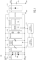
- FIG. 1 illustrates, in simplified block diagram form, an example ultra-high frequency (UHF) RFID frontend 100 with an antenna tuning circuit in accordance with an embodiment.
- the example RFID frontend 100 is implemented in one or more complementary metal-oxide semiconductor (CMOS) integrated circuits.
- the RFID frontend 100 includes an electrostatic discharge (ESD) protection circuit 102, an RF limiter circuit 104, an antenna tuning impedance circuit 106, a modulator circuit 108, a demodulator circuit 110, a rectifier circuit 112, a DC limiter circuit 114, and a buffer capacitor 124.
- the demodulator circuit 110 includes an envelope detector circuit 120 and a comparator circuit indicated by dashed outlines.
- the RFID frontend 100 further includes an antenna tuning control circuit 116 and an antenna tuning detector circuit 118.
- the ESD protection circuit 102, RF limiter circuit 104, antenna tuning impedance circuit 106, modulator circuit 108, envelope detector circuit 120 of the demodulator circuit 110, and rectifier circuit 112 are coupled to differential antenna terminals RF1 and RF2.
- An antenna (not shown) is connected to the respective antenna terminals RF1 and RF2.
- the DC limiter circuit 114 includes an input connected to an output of the rectifier circuit 112, and an output connected to a power supply voltage terminal labeled VDDA.
- the buffer capacitor 124 includes a first terminal connected to VDDA and a second terminal connected to a ground voltage terminal labeled GND.
- the antenna tuning detector circuit 118 is coupled to the envelope detector circuit 120 of the demodulator circuit 110 and the antenna tuning control circuit 116 is coupled to the antenna tuning impedance circuit 106.
- the rectifier circuit 112 is configured to provide transformation of the received RF voltage from the antenna connected at the antenna terminals RF1 and RF2 to provide a DC supply voltage for circuits of an integrated circuit (IC) (e.g., digital logic, non-volatile memory).
- IC integrated circuit
- the modulator circuit 108 is configured to provide modulation of an input impedance to modulate the signal that is scattered back from the antenna to transmit information to a reader, for example.
- the demodulator circuit 110 is configured to provide demodulation of an amplitude modulated signal transmitted by a reader and received at the antenna connected to antenna terminals RF1 and RF2, for example.
- the antenna tuning impedance circuit 106 is configured to provide tuning of the input impedance (e.g., tunable capacitance) to maximize the power transfer from the antenna to the chip input.
- the antenna tuning control circuit 116 is configured to control the execution of an antenna tuning procedure to adjust impedance settings by way of control signal(s) provided to the antenna tuning impedance circuit 106.
- the antenna tuning control circuit 116 may be implemented as a digital logic circuit block, for example.
- the antenna tuning detector circuit 118 is configured to detect changes of the RF voltage amplitude in response to adjustments of the tuning impedance by the antenna tuning control circuit 116. An output of the antenna tuning detector circuit 118 provides an indication to the antenna tuning control circuit 116 whether an applied impedance adjustment improved the power transfer.
- the electrostatic discharge protection circuit 102 may be implemented in various ways.
- One example implementation of ESD protection circuit 102 includes anti-parallel pn-junction diodes.
- the anti-parallel diodes are configured to provide a path for high currents generated by an electrostatic discharge event at the antenna terminals that may otherwise damage circuits on the integrated circuit.
- the DC limiter circuit 114 is configured to regulate and limit the output voltage of the rectifier circuit 112.
- circuit blocks, arrangement, connectivity, and symbols within these circuit blocks of the RFID frontend 100 are chosen for illustration purposes. Note that even though a differential RFID frontend implementation is depicted in FIG. 1 and described, a single-ended frontend implementation may be provided in which either terminal RF1 and RF2 corresponds to the IC ground.
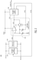
- FIG. 2 illustrates, in simplified schematic diagram form, an example of an antenna tuning circuit 200 of the RFID frontend 100 in accordance with an embodiment.
- the antenna tuning circuit 200 includes antenna tuning impedance circuit 202, envelope detector circuit 204, antenna tuning detector circuit 206, and antenna tuning control circuit 208.
- the antenna tuning impedance circuit 202, envelope detector circuit 204, antenna tuning detector circuit 206, and antenna tuning control circuit 208 of the antenna tuning circuit 200 correspond to the antenna tuning impedance circuit 106, envelope detector circuit 120, antenna tuning detector circuit 118, and antenna tuning control circuit 116 of the RFID frontend 100 depicted in FIG. 1 .
- the antenna tuning impedance circuit 202 includes an impedance matching network coupled to the antenna terminals RF1 and RF2 and has an input coupled to receive tuning control signal labeled TCTRL from the antenna tuning control circuit 208.
- the antenna tuning impedance circuit 202 for example, has selectable load capacitance for adjusting (e.g., tuning) impedance across the antenna terminals RF1 and RF2.
- the tunable impedance of the antenna tuning impedance circuit 202 is controlled by way to the tuning control signal TCTRL.
- the RF input voltage amplitude is maximized by way of tuning the impedance coupled to the antenna terminals RF1 and RF2.
- the envelope detector circuit 204 is coupled to the antenna terminals RF1 and RF2 and configured to provide at an output envelope signal labeled VENV that tracks the voltage envelope of the differential RF voltage at the antenna terminals RF1 and RF2.
- the output envelope signal VENV of the envelope detector circuit 204 is based on the extracted voltage envelope of the received RF voltage signal at RF1 and RF2.
- an example implementation of the antenna tuning detector circuit 206 includes an operational amplifier 210, a switch labeled SW, a sample capacitor Cs, and an offset capacitor Co.
- the operational amplifier 210 includes a non-inverting (+) input coupled to the output of the envelope detector circuit 204, an inverting input (-) coupled to a first terminal capacitor Cs, a first terminal of capacitor Co, and a first terminal of switch SW at node labeled VS, and an output labeled OUT coupled to an input of the antenna tuning control circuit 208 to provide an output signal OUT.
- a second terminal of the capacitor Cs is coupled to the ground terminal GND and a second terminal of the switch SW is coupled at the output OUT.
- a second terminal of the capacitor Co is coupled to a control terminal of the switch SW at node labeled CTRL.
- the second terminal of the capacitor Co and the control terminal of the switch SW are coupled to receive control signal labeled CTRL from the antenna tuning control circuit 208.
- the antenna tuning control circuit 208 has a first input to receive a clock signal labeled CLK, a second input to receive the OUT signal from the operational amplifier 210, a first output for providing the control signal CTRL, a second output for providing the tuning control signal TCTRL, and a third output for providing a completion signal labeled COMPLETE.
- the operational amplifier 210 has an input connected to a digital power supply voltage terminal labeled VDDD and the ground terminal GND (not shown).
- the antenna tuning control circuit 208 has an input connected to the digital power supply voltage terminal VDDD and the ground terminal GND (not shown).
- the antenna tuning control circuit 208 includes clocked logic implementing an auto-tuning sequence based on phase of operation.
- the tuning control circuit 208 is configured to generate the control signal CTRL and the tuning control signal TCTRL based on the output signal OUT of the operational amplifier 210.
- the switch SW is closed connecting the output OUT to the node VS allowing the voltage at the output OUT to substantially equal the voltage of the VENV signal.
- the voltage at the output OUT may be equal to a first voltage of the VENV signal VENVO minus an offset voltage VOS (e.g., offset voltage of the operational amplifier, approximately 10-20 millivolts).
- the antenna tuning control circuit 208 applies a next configuration of the antenna tuning impedance according to an antenna tuning procedure by way of tuning control signal TCTRL.
- the tuning control signal TCTRL may be implemented as a plurality of signal lines, for example.
- the operational amplifier 210 is configured to generate the output signal OUT as a logic value (e.g., logic 0 or logic 1) by comparing a second voltage VENV1 of the VENV signal with the voltage of the VS signal at the node VS.
- the VENV1 voltage may be different from VENVO voltage as a result of a changed antenna tuning impedance configuration.
- the VS voltage serves as a reference voltage for the comparator function of the operational amplifier 210 in the comparator configuration.
- the VS voltage is approximately equal to the sampled first envelope detector voltage VENVO minus the offset voltage VOS plus ⁇ V which is equal to VDDD voltage multiplied by the ratio of Co to Cs (i.e., VDDD*Co/Cs).
- the antenna tuning control circuit 208 receives the logic value of the OUT signal and determines whether the applied antenna tuning impedance configuration has resulted in a sufficient increase of VENV.
- An increase in VENV corresponds to an increased power transfer from the antenna to the RFID frontend circuit as a result of an improved impedance matching between antenna and RFID frontend circuit or RFID transponder.
- the auto-tuning sequence of the antenna tuning control circuit 208 continues by adjusting the impedance coupled to the antenna terminals RF1 and RF2 and alternating sample and hold phases. By monitoring successive output envelope signal VENV voltage values for each impedance adjustment, an optimum (e.g., maximum) RF voltage amplitude is identified and set. After the optimum voltage amplitude is set, the antenna tuning control circuit 208 provides an indication that the auto-tuning is complete by way of the completion signal COMPLETE.
- FIG. 3A illustrates, in simplified schematic diagram form, the antenna tuning detector 206 of FIG. 2 configured in a follower configuration 302 in accordance with an embodiment.
- the antenna tuning detector follower configuration 302 includes operational amplifier OA, switch SW configured in a closed state, sample capacitor Cs, and offset capacitor Co.
- the operational amplifier OA includes the non-inverting (+) input coupled to receive the VENV envelope signal, inverting input (-) coupled to the first terminal of capacitor Cs, the first terminal of capacitor Co, and to the output OUT by way of the closed switch SW.
- the second terminal of the capacitor Cs is coupled to the ground terminal GND and the second terminal of the capacitor Co is coupled to the control terminal of the switch SW at node CTRL.
- the second terminal of the capacitor Co and the control terminal of the switch SW are coupled to receive the CTRL control signal (e.g., GND).
- the switch SW is closed forming a conductive path from the output OUT to the node VS.
- the operational amplifier OA With the switch SW closed, the operational amplifier OA is essentially in a unity gain configuration allowing the voltage at the output OUT to be substantially equal to a first voltage VENVO of the VENV signal minus an offset voltage VOS.
- VENVO first voltage
- VOS offset voltage
- each of the capacitors Cs and Co are charged to the voltage level of the OUT signal while in the follower configuration 302.
- Corresponding follower configuration sample waveforms of the VENV, VS, OUT, and CTRL signals are illustrated in phase 0 of FIG. 4 .
- FIG. 3B illustrates, in simplified schematic diagram form, the antenna tuning detector 206 of FIG. 2 configured in a comparator configuration 304 in accordance with an embodiment.
- the antenna tuning detector comparator configuration 304 includes operational amplifier OA, switch SW configured in an open state, sample capacitor Cs, and offset capacitor Co.
- the operational amplifier OA includes the non-inverting (+) input coupled to receive the VENV envelope signal, inverting input (-) coupled to the first terminal of capacitor Cs and the first terminal of capacitor Co.
- the second terminal of the capacitor Cs is coupled to the ground terminal GND and the second terminal of the capacitor Co is coupled to the control terminal of the switch SW at node CTRL.
- the second terminal of the capacitor Co and the control terminal of the switch SW are coupled to receive the CTRL control signal (e.g., VDDD).
- the output OUT is isolated from node VS by way of the opened switch SW and the VDDD voltage is applied to the second terminal of the capacitor Co.
- the operational amplifier OA is configured to compare a second voltage VENV1 of the VENV signal with the voltage of the VS signal at the node VS and provide a logic value at the output OUT.
- the VS voltage serves as a reference voltage for the comparator function of the operational amplifier OA in the comparator configuration.
- the VS voltage is boosted by a delta voltage ⁇ V (e.g., ⁇ V of approximately 10 millivolts) by injecting the charge stored in the capacitor Co such that the resulting VS voltage is approximately equal to VENVO minus the offset voltage VOS plus VDDD*Co/Cs when the control signal CTRL transitions from the GND voltage to the VDDD voltage.
- ⁇ V delta voltage
- Corresponding comparator configuration sample waveforms of the VENV, VS, OUT, and CTRL signals are illustrated in phase 1 of FIG. 4 .
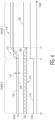
- FIG. 4 illustrates, in simplified plot diagram form, example signal waveforms of the antenna tuning detector circuitry depicted in FIG. 3A and FIG. 3B in accordance with an embodiment.
- the plot diagram of FIG. 4 includes a VENV voltage signal waveform 402, a VS voltage signal waveform 404, and an OUT signal waveform 408 corresponding to the respective input and output signals of the operational amplifier OA FIG. 3A and FIG. 3B .
- the plot diagram of FIG. 4 further includes a CTRL control signal waveform 410 of the antenna tuning detector circuitry depicted in FIG. 3A and FIG. 3B .
- Example signal waveforms of the antenna tuning detector circuitry are shown versus TIME on the X-axis. By way of example, basic operation of the antenna tuning detector circuitry is depicted in the following.
- the antenna tuning detector circuitry is in a first phase of operation labeled PHASE 0.
- the VENV, VS, OUT, and CTRL waveforms correspond to the circuit configuration depicted in FIG. 3A with the operational amplifier OA configured in the follower configuration.
- the control signal CTRL is at a logic 0 level (e.g., GND) which configures the operation amplifier OA in the follower configuration.
- the VENV voltage level minus offset voltage VOS 412 is provided to the VS node.
- the PHASE 0 phase may be characterized as a sample phase in which the voltage level at the VS node is sampled by way of charging the Cs and Co capacitors to the VS node voltage.
- the OUT signal waveform 408 includes a non-valid region 418 (e.g., depicted as a crossed-hatch region) from a logic level perspective.
- the OUT signal is essentially an analog signal during PHASE 0 and not necessarily indicative of a logic value.
- the VENV voltage is at a first voltage level VENVO.
- the CTRL control signal transitions from a logic 0 level to a logic 1 level (e.g., VDDD) and the antenna tuning detector circuitry enters a second phase of operation labeled PHASE 1.
- a logic 1 level e.g., VDDD
- the VENV, VS, OUT, and CTRL waveforms correspond to the circuit configuration depicted in FIG. 3B with the operational amplifier OA configured in the comparator configuration.
- the transition of the CTRL control signal to the logic 1 level configures the operation amplifier OA in the comparator configuration by way of opening the switch SW.
- the transition from GND to VDDD at the second terminal of the capacitor Co causes the Co stored charge to be injected at the VS node such that the VS voltage 404 transitions to a boosted VS voltage level 414 approximately equal to VENVO minus the offset voltage VOS plus VDDD*Co/Cs.
- the PHASE 1 phase may be characterized as a hold phase in which the boosted VS voltage level 414 at the VS node is held at approximately VENVO minus the offset VOS plus ⁇ V until the next sample phase, for example.
- the VENV voltage level minus the offset voltage VOS 412 is shown as a dashed line 406 for reference.
- the antenna tuning detector circuitry is at the PHASE 1 phase of operation.
- the VENV voltage transitions to a second voltage level VENV1 416 in response to a tuning step adjustment to the tunable impedance of the antenna tuning impedance circuit in this embodiment.
- the VENV voltage 416 exceeds the boosted VS voltage 414 by an amount sufficient to cause the OUT signal of the comparator function to transition to a logic 1 level.
- the OUT signal at the logic 1 level provides an indication to the antenna tuning control circuit that the tuning step adjustment to the tunable impedance of the antenna tuning circuit generated an improved RF input voltage amplitude.
- FIG. 5 illustrates, in simplified flow diagram form, an example method for antenna tuning in accordance with an embodiment.
- the example antenna auto-tuning method 500 corresponds to the example antenna tuning circuit 200 of the RFID frontend 100 depicted in FIG. 2 .
- a first voltage VENVO of the VENV voltage signal from the envelope detector circuit 204 at a first antenna tuning state is sampled by way of the antenna tuning detector 206 configured in the follower configuration.
- the first voltage VENVO of the VENV voltage signal (e.g., minus an intrinsic offset voltage of the operational amplifier) is provided as a voltage VS0 to the VS node and stored on the Cs and Co capacitors.
- the antenna tuning detector 206 is configured in the comparator configuration.
- a second voltage VENV1 of the VENV voltage signal at the non-inverting input (+) is compared with the VS0 voltage plus ⁇ V at the inverting (e.g., reference) input (-).
- the VENV1 voltage is greater than the VS0 voltage plus ⁇ V
- the OUT signal transitions to a logic high level (e.g., logic 1 level, VDDD), for example.
- the predetermined threshold ⁇ V is generated by the transition of the control signal CTRL from logic 0 to logic 1 level applied to the capacitor Co.
- step 506 determine whether the sampled voltage is greater than the reference voltage (e.g., VS voltage). If the VENV1 voltage is not greater than the VS0 voltage plus ⁇ V (reference) voltage, then (NO) the optimal antenna tuning impedance state has been reached and the antenna tuning procedure is completed. If the VENV1 voltage is greater than the VS0 voltage plus ⁇ V (reference) voltage, then (YES) the optimal antenna tuning impedance state has not been reached and the antenna tuning procedure continues at step 508.
- the reference voltage e.g., VS voltage
- step 508 adjust antenna impedance.
- an antenna tuning impedance state is applied by the antenna tuning control circuit to the antenna tuning impedance circuit 202 by way of the TCTRL signal.
- the antenna tuning control circuit 208 provides the TCTRL tuning control signal based on the OUT signal of the operational amplifier in the comparator configuration.
- an antenna tuning circuit for radio frequency identification (RFID) transponders including an envelope detector having an input coupled to an antenna terminal, the envelope detector configured to track an envelope of a signal received at the antenna terminal, the envelope detector having an output for providing a first signal; an operational amplifier having a first input coupled to the output of the envelope detector to receive the first signal and a second input coupled to receive a second signal, the operational amplifier configured to generate an output signal at an output based on the first signal and the second signal; a switch having a first terminal coupled to the output of the operational amplifier, a second terminal coupled to the second input of the operational amplifier, and a control terminal coupled to receive a first control signal, wherein the operational amplifier is configured in a follower configuration when the first control signal is at a first voltage value.
- RFID radio frequency identification
- the operational amplifier may be further configured in a comparator configuration when the first control signal is at a second voltage value.
- the antenna tuning circuit may be configured in a sample phase when the first control signal is at the first voltage value and configured in a hold phase when the first control signal is at the second voltage value.
- the antenna tuning circuit may further include a first capacitor having a first terminal coupled at the second input of the operational amplifier, and a second terminal coupled at a ground terminal; and a second capacitor having a first terminal coupled at the second input of the operational amplifier, and a second terminal coupled to receive the first control signal.
- the second capacitor may be configured to store a voltage; and inject stored charge at the second input of the operational amplifier when the first control signal transitions from the first voltage value to the second voltage value.
- the antenna tuning circuit may further include a tuning control circuit having an input coupled to the output of the operational amplifier, the tuning control circuit configured to generate the first control signal at a first output based on the output signal of the operational amplifier.
- the tuning control circuit may be further configured to generate a second control signal at a second output based on the output signal of the operational amplifier, the second control signal configured for adjustment of impedance at the antenna terminal.
- the antenna tuning circuit may further include a matching network coupled to the antenna terminal, the matching network configured to adjust impedance at the antenna terminal in response to the second control signal.
- the output signal at the output of the operational amplifier may be characterized as logically invalid when the first control signal is at the first voltage value.
- a method including tracking an envelope of a radio frequency signal received at an antenna terminal to produce a first signal; sampling a first voltage of the first signal by way of an operational amplifier in a first configuration; comparing the first voltage of the first signal with a reference voltage by way of the operational amplifier in a second configuration; and adjusting impedance at the antenna terminal based on the comparison of the first voltage of the first signal with the reference voltage.
- the method may further include generating a first control signal based on an output logic value of the operational amplifier in the second configuration, the impedance at the antenna terminal adjusted by way of the first control signal.
- the method may further include controlling a switch by way of a second control signal, the operational amplifier configured in the first configuration in response to the second control signal at a first state and in the second configuration in response to the second control signal at a second state.
- the first configuration of the operational amplifier may be characterized as a follower configuration and the second configuration of the operational amplifier is characterized as a comparator configuration.
- the method may further include storing the first voltage by way of a first capacitor coupled at a first input of the operational amplifier in the first configuration; and injecting stored charge corresponding to an offset voltage by way of a second capacitor coupled at the first input of the operational amplifier in the second configuration.
- the offset voltage may be proportional to the ratio of the second capacitor capacitance to the first capacitor capacitance.
- an antenna tuning circuit for radio frequency identification (RFID) transponders including an envelope detector having an input coupled to an antenna terminal, the envelope detector configured to track an envelope of a signal received at the antenna terminal, the envelope detector having an output for providing a first signal; an operational amplifier having a first input coupled to the output of the envelope detector to receive the first signal and a second input coupled to receive a second signal, the operational amplifier configured to generate an output signal at an output based on the first signal and the second signal; a switch having a first terminal coupled to the output of the operational amplifier, a second terminal coupled to the second input of the operational amplifier, and a control terminal coupled to receive a first control signal, wherein the operational amplifier is configured in a follower configuration when the first control signal is at a first voltage value and configured in a comparator configuration when the first control signal is at a second voltage value; and a tuning control circuit having an input coupled to the output of the operational amplifier, the tuning control circuit configured to generate the first control signal at a first output based on the output
- RFID radio frequency identification
- the tuning control circuit may be further configured to generate a second control signal at a second output based on the output signal of the operational amplifier, the second control signal configured for adjustment of impedance at the antenna terminal.
- the antenna tuning circuit may be configured in a sample phase when the first control signal is at the first voltage value and configured in a hold phase when the first control signal is at the second voltage value.
- the antenna tuning circuit may further include a first capacitor having a first terminal coupled at the second input of the operational amplifier, and a second terminal coupled at a ground terminal; and a second capacitor having a first terminal coupled at the second input of the operational amplifier, and a second terminal coupled to receive the first control signal.
- the second capacitor may be configured to store a voltage; and inject stored charge at the second input of the operational amplifier when the first control signal transitions from the first voltage value to the second voltage value.
- an antenna tuning circuit for a UHF RFID transponder that includes an antenna tuning impedance circuit, envelope detector circuit, antenna tuning detector circuit, and antenna tuning control circuit.
- the antenna tuning impedance circuit includes an adjustable impedance to adjust an impedance coupled to the antenna terminals of the RFID transponder.
- the envelope detector provides an envelope signal that tracks a voltage envelope of a signal received at an antenna.
- the antenna tuning control provides a first control signal to control the antenna tuning detector and provides a second control signal or a control signal bus to configure the antenna tuning impedance circuit.
- the antenna tuning control includes digital circuitry to execute a procedure to apply in sequential steps different configurations of the antenna tuning impedance.
- the antenna tuning detector includes an operational amplifier that is configured in a follower configuration during a first phase of an applied tuning impedance configuration and configured in a comparator configuration during a second phase of changed applied tuning impedance configuration.
- the antenna tuning controller includes clock-based circuitry and provides a first control signal to configure the operation amplifier.
- the antenna tuning detector samples the voltage of the envelop signal during the first phase.
- the antenna tuning detector compares a present voltage of the envelop signal with the previously sampled voltage of the envelop signal and provides a digital output signal. Based on the digital output signal, the antenna tuning controller determines the antenna tuning impedance configuration to be applied in the next sequential step. In this manner, automatic adjustments to the impedance matching between the antenna and the frontend circuit of the RFID transponder to optimize the power transfer to the frontend circuitry can be realized.
Landscapes
- Engineering & Computer Science (AREA)
- Physics & Mathematics (AREA)
- Power Engineering (AREA)
- General Physics & Mathematics (AREA)
- Toxicology (AREA)
- Health & Medical Sciences (AREA)
- Theoretical Computer Science (AREA)
- Computer Networks & Wireless Communication (AREA)
- Electromagnetism (AREA)
- General Health & Medical Sciences (AREA)
- Artificial Intelligence (AREA)
- Computer Vision & Pattern Recognition (AREA)
- Computer Hardware Design (AREA)
- Microelectronics & Electronic Packaging (AREA)
- Input Circuits Of Receivers And Coupling Of Receivers And Audio Equipment (AREA)
Abstract
Description
- This disclosure relates generally to electronic circuits, and more specifically, to an antenna tuning circuit for radio frequency identification (RFID) transponders.
- Ultra-high frequency (UHF) RFID transponders, commonly referred to as RFID tags, are widely used to identify objects to which the tags are attached. The most common application examples of RFID tags are retail, supply chain management, shipping services, airline luggage tracking, laundry services, etc. An RFID tag typically includes an antenna and an integrated circuit. In such configurations, the integrated circuit is powered by voltage derived from a received RF signal. An RFID transponder may communicate with an RFID reader via an electrical, magnetic, or electromagnetic field generated by the RFID reader. It is therefore desirable to provide an efficient power conversion from RF signals.
- The present invention is illustrated by way of example and is not limited by the accompanying figures, in which like references indicate similar elements. Elements in the figures are illustrated for simplicity and clarity and have not necessarily been drawn to scale.
-
FIG. 1 illustrates, in simplified block diagram form, an example ultra-high frequency (UHF) RFID frontend with an antenna tuning circuit in accordance with an embodiment. -
FIG. 2 illustrates, in simplified schematic diagram form, an example antenna tuning circuit in accordance with an embodiment. -
FIG. 3A and FIG. 3B illustrate, in simplified schematic diagram form, circuitry of the example an antenna tuning detector at phases of operation in accordance with an embodiment. -
FIG. 4 illustrates, in simplified plot diagram form, example signal waveforms of the antenna tuning detector circuitry depicted inFIG. 3A and FIG. 3B in accordance with an embodiment. -
FIG. 5 illustrates, in simplified flow diagram form, an example method for antenna tuning in accordance with an embodiment. - Generally, there is provided, an antenna tuning circuit for a UHF RFID transponder that includes an antenna tuning impedance circuit, envelope detector circuit, antenna tuning detector circuit, and antenna tuning control circuit. The antenna tuning impedance circuit includes an adjustable impedance to adjust an impedance coupled to the antenna terminals of the RFID transponder. The envelope detector provides an envelope signal that tracks a voltage envelope of a signal received at an antenna. The antenna tuning control provides a first control signal to control the antenna tuning detector and provides a second control signal or a control signal bus to configure the antenna tuning impedance circuit. The antenna tuning control includes digital circuitry to execute a procedure to apply in sequential steps different configurations of the antenna tuning impedance. The antenna tuning detector includes an operational amplifier that is configured in a follower configuration during a first phase of an applied tuning impedance configuration and configured in a comparator configuration during a second phase of changed applied tuning impedance configuration. The antenna tuning controller includes clock-based circuitry and provides a first control signal to configure the operation amplifier. The antenna tuning detector samples the voltage of the envelop signal during the first phase. During the second phase, the antenna tuning detector compares a present voltage of the envelop signal with the previously sampled voltage of the envelop signal and provides a digital output signal. Based on the digital output signal, the antenna tuning controller determines the antenna tuning impedance configuration to be applied in the next sequential step. In this manner, automatic adjustments to the impedance matching between the antenna and the frontend circuit of the RFID transponder to optimize the power transfer to the frontend circuitry can be realized.
-
FIG. 1 illustrates, in simplified block diagram form, an example ultra-high frequency (UHF)RFID frontend 100 with an antenna tuning circuit in accordance with an embodiment. In this embodiment, theexample RFID frontend 100 is implemented in one or more complementary metal-oxide semiconductor (CMOS) integrated circuits. TheRFID frontend 100 includes an electrostatic discharge (ESD)protection circuit 102, anRF limiter circuit 104, an antennatuning impedance circuit 106, amodulator circuit 108, ademodulator circuit 110, arectifier circuit 112, aDC limiter circuit 114, and abuffer capacitor 124. Thedemodulator circuit 110 includes anenvelope detector circuit 120 and a comparator circuit indicated by dashed outlines. In this embodiment, theRFID frontend 100 further includes an antennatuning control circuit 116 and an antennatuning detector circuit 118. - The
ESD protection circuit 102,RF limiter circuit 104, antennatuning impedance circuit 106,modulator circuit 108,envelope detector circuit 120 of thedemodulator circuit 110, andrectifier circuit 112 are coupled to differential antenna terminals RF1 and RF2. An antenna (not shown) is connected to the respective antenna terminals RF1 and RF2. TheDC limiter circuit 114 includes an input connected to an output of therectifier circuit 112, and an output connected to a power supply voltage terminal labeled VDDA. Thebuffer capacitor 124 includes a first terminal connected to VDDA and a second terminal connected to a ground voltage terminal labeled GND. In this embodiment, the antennatuning detector circuit 118 is coupled to theenvelope detector circuit 120 of thedemodulator circuit 110 and the antennatuning control circuit 116 is coupled to the antennatuning impedance circuit 106. - The
rectifier circuit 112 is configured to provide transformation of the received RF voltage from the antenna connected at the antenna terminals RF1 and RF2 to provide a DC supply voltage for circuits of an integrated circuit (IC) (e.g., digital logic, non-volatile memory). Themodulator circuit 108 is configured to provide modulation of an input impedance to modulate the signal that is scattered back from the antenna to transmit information to a reader, for example. Thedemodulator circuit 110 is configured to provide demodulation of an amplitude modulated signal transmitted by a reader and received at the antenna connected to antenna terminals RF1 and RF2, for example. The antennatuning impedance circuit 106 is configured to provide tuning of the input impedance (e.g., tunable capacitance) to maximize the power transfer from the antenna to the chip input. - In this embodiment, the antenna
tuning control circuit 116 is configured to control the execution of an antenna tuning procedure to adjust impedance settings by way of control signal(s) provided to the antennatuning impedance circuit 106. The antennatuning control circuit 116 may be implemented as a digital logic circuit block, for example. The antennatuning detector circuit 118 is configured to detect changes of the RF voltage amplitude in response to adjustments of the tuning impedance by the antennatuning control circuit 116. An output of the antennatuning detector circuit 118 provides an indication to the antennatuning control circuit 116 whether an applied impedance adjustment improved the power transfer. - The electrostatic
discharge protection circuit 102 may be implemented in various ways. One example implementation ofESD protection circuit 102 includes anti-parallel pn-junction diodes. The anti-parallel diodes are configured to provide a path for high currents generated by an electrostatic discharge event at the antenna terminals that may otherwise damage circuits on the integrated circuit. TheDC limiter circuit 114 is configured to regulate and limit the output voltage of therectifier circuit 112. - The number of circuit blocks, arrangement, connectivity, and symbols within these circuit blocks of the
RFID frontend 100 are chosen for illustration purposes. Note that even though a differential RFID frontend implementation is depicted inFIG. 1 and described, a single-ended frontend implementation may be provided in which either terminal RF1 and RF2 corresponds to the IC ground. -
FIG. 2 illustrates, in simplified schematic diagram form, an example of anantenna tuning circuit 200 of theRFID frontend 100 in accordance with an embodiment. Theantenna tuning circuit 200 includes antennatuning impedance circuit 202,envelope detector circuit 204, antennatuning detector circuit 206, and antennatuning control circuit 208. In this embodiment, the antennatuning impedance circuit 202,envelope detector circuit 204, antennatuning detector circuit 206, and antennatuning control circuit 208 of theantenna tuning circuit 200 correspond to the antennatuning impedance circuit 106,envelope detector circuit 120, antennatuning detector circuit 118, and antennatuning control circuit 116 of theRFID frontend 100 depicted inFIG. 1 . - The antenna
tuning impedance circuit 202 includes an impedance matching network coupled to the antenna terminals RF1 and RF2 and has an input coupled to receive tuning control signal labeled TCTRL from the antennatuning control circuit 208. The antennatuning impedance circuit 202, for example, has selectable load capacitance for adjusting (e.g., tuning) impedance across the antenna terminals RF1 and RF2. The tunable impedance of the antennatuning impedance circuit 202 is controlled by way to the tuning control signal TCTRL. The RF input voltage amplitude is maximized by way of tuning the impedance coupled to the antenna terminals RF1 and RF2. - The
envelope detector circuit 204 is coupled to the antenna terminals RF1 and RF2 and configured to provide at an output envelope signal labeled VENV that tracks the voltage envelope of the differential RF voltage at the antenna terminals RF1 and RF2. The output envelope signal VENV of theenvelope detector circuit 204 is based on the extracted voltage envelope of the received RF voltage signal at RF1 and RF2. - In this embodiment, an example implementation of the antenna
tuning detector circuit 206 includes anoperational amplifier 210, a switch labeled SW, a sample capacitor Cs, and an offset capacitor Co. Theoperational amplifier 210 includes a non-inverting (+) input coupled to the output of theenvelope detector circuit 204, an inverting input (-) coupled to a first terminal capacitor Cs, a first terminal of capacitor Co, and a first terminal of switch SW at node labeled VS, and an output labeled OUT coupled to an input of the antennatuning control circuit 208 to provide an output signal OUT. A second terminal of the capacitor Cs is coupled to the ground terminal GND and a second terminal of the switch SW is coupled at the output OUT. A second terminal of the capacitor Co is coupled to a control terminal of the switch SW at node labeled CTRL. The second terminal of the capacitor Co and the control terminal of the switch SW are coupled to receive control signal labeled CTRL from the antennatuning control circuit 208. - The antenna
tuning control circuit 208 has a first input to receive a clock signal labeled CLK, a second input to receive the OUT signal from theoperational amplifier 210, a first output for providing the control signal CTRL, a second output for providing the tuning control signal TCTRL, and a third output for providing a completion signal labeled COMPLETE. Theoperational amplifier 210 has an input connected to a digital power supply voltage terminal labeled VDDD and the ground terminal GND (not shown). Likewise, the antennatuning control circuit 208 has an input connected to the digital power supply voltage terminal VDDD and the ground terminal GND (not shown). - The antenna
tuning control circuit 208 includes clocked logic implementing an auto-tuning sequence based on phase of operation. Thetuning control circuit 208 is configured to generate the control signal CTRL and the tuning control signal TCTRL based on the output signal OUT of theoperational amplifier 210. In a first (e.g., sample) phase of operation, the antennatuning control circuit 208 configures theoperational amplifier 210 in a "follower" configuration by way of the control signal CTRL at a first state (e.g., CTRL=GND). In a second (e.g., hold) phase of operation, the antennatuning control circuit 208 configures theoperational amplifier 210 in a "comparator" configuration by way of the control signal CTRL at a second state (e.g., CTRL=VDDD). - In the follower configuration, the switch SW is closed connecting the output OUT to the node VS allowing the voltage at the output OUT to substantially equal the voltage of the VENV signal. For example, the voltage at the output OUT may be equal to a first voltage of the VENV signal VENVO minus an offset voltage VOS (e.g., offset voltage of the operational amplifier, approximately 10-20 millivolts). The voltage (VS) at the node VS coupled to the output OUT may be represented as VS=VENVO-VOS. Accordingly, each of the capacitors Cs and Co are charged to the voltage level of the output OUT and VS.
- In the comparator configuration, the switch is opened and the VDDD voltage is applied to the second terminal of the capacitor Co. Therefore, a delta voltage ΔV equal to VDDD*Co/Cs is injected at node VS. The antenna
tuning control circuit 208 applies a next configuration of the antenna tuning impedance according to an antenna tuning procedure by way of tuning control signal TCTRL. The tuning control signal TCTRL may be implemented as a plurality of signal lines, for example. Theoperational amplifier 210 is configured to generate the output signal OUT as a logic value (e.g., logic 0 or logic 1) by comparing a second voltage VENV1 of the VENV signal with the voltage of the VS signal at the node VS. It should be noted that the VENV1 voltage may be different from VENVO voltage as a result of a changed antenna tuning impedance configuration. The VS voltage serves as a reference voltage for the comparator function of theoperational amplifier 210 in the comparator configuration. In this embodiment, the VS voltage is approximately equal to the sampled first envelope detector voltage VENVO minus the offset voltage VOS plus ΔV which is equal to VDDD voltage multiplied by the ratio of Co to Cs (i.e., VDDD*Co/Cs). The antennatuning control circuit 208 receives the logic value of the OUT signal and determines whether the applied antenna tuning impedance configuration has resulted in a sufficient increase of VENV. An increase in VENV corresponds to an increased power transfer from the antenna to the RFID frontend circuit as a result of an improved impedance matching between antenna and RFID frontend circuit or RFID transponder. - The auto-tuning sequence of the antenna
tuning control circuit 208 continues by adjusting the impedance coupled to the antenna terminals RF1 and RF2 and alternating sample and hold phases. By monitoring successive output envelope signal VENV voltage values for each impedance adjustment, an optimum (e.g., maximum) RF voltage amplitude is identified and set. After the optimum voltage amplitude is set, the antennatuning control circuit 208 provides an indication that the auto-tuning is complete by way of the completion signal COMPLETE. -
FIG. 3A illustrates, in simplified schematic diagram form, theantenna tuning detector 206 ofFIG. 2 configured in afollower configuration 302 in accordance with an embodiment. The antenna tuningdetector follower configuration 302 includes operational amplifier OA, switch SW configured in a closed state, sample capacitor Cs, and offset capacitor Co. The operational amplifier OA includes the non-inverting (+) input coupled to receive the VENV envelope signal, inverting input (-) coupled to the first terminal of capacitor Cs, the first terminal of capacitor Co, and to the output OUT by way of the closed switch SW. The second terminal of the capacitor Cs is coupled to the ground terminal GND and the second terminal of the capacitor Co is coupled to the control terminal of the switch SW at node CTRL. The second terminal of the capacitor Co and the control terminal of the switch SW are coupled to receive the CTRL control signal (e.g., GND). - In the
follower configuration 302, the switch SW is closed forming a conductive path from the output OUT to the node VS. With the switch SW closed, the operational amplifier OA is essentially in a unity gain configuration allowing the voltage at the output OUT to be substantially equal to a first voltage VENVO of the VENV signal minus an offset voltage VOS. As a result, each of the capacitors Cs and Co are charged to the voltage level of the OUT signal while in thefollower configuration 302. Corresponding follower configuration sample waveforms of the VENV, VS, OUT, and CTRL signals are illustrated in phase 0 ofFIG. 4 . -
FIG. 3B illustrates, in simplified schematic diagram form, theantenna tuning detector 206 ofFIG. 2 configured in acomparator configuration 304 in accordance with an embodiment. The antenna tuningdetector comparator configuration 304 includes operational amplifier OA, switch SW configured in an open state, sample capacitor Cs, and offset capacitor Co. The operational amplifier OA includes the non-inverting (+) input coupled to receive the VENV envelope signal, inverting input (-) coupled to the first terminal of capacitor Cs and the first terminal of capacitor Co. The second terminal of the capacitor Cs is coupled to the ground terminal GND and the second terminal of the capacitor Co is coupled to the control terminal of the switch SW at node CTRL. The second terminal of the capacitor Co and the control terminal of the switch SW are coupled to receive the CTRL control signal (e.g., VDDD). - In the
comparator configuration 304, the output OUT is isolated from node VS by way of the opened switch SW and the VDDD voltage is applied to the second terminal of the capacitor Co. The operational amplifier OA is configured to compare a second voltage VENV1 of the VENV signal with the voltage of the VS signal at the node VS and provide a logic value at the output OUT. The VS voltage serves as a reference voltage for the comparator function of the operational amplifier OA in the comparator configuration. In this embodiment, the VS voltage is boosted by a delta voltage ΔV (e.g., ΔV of approximately 10 millivolts) by injecting the charge stored in the capacitor Co such that the resulting VS voltage is approximately equal to VENVO minus the offset voltage VOS plus VDDD*Co/Cs when the control signal CTRL transitions from the GND voltage to the VDDD voltage. Corresponding comparator configuration sample waveforms of the VENV, VS, OUT, and CTRL signals are illustrated inphase 1 ofFIG. 4 . -
FIG. 4 illustrates, in simplified plot diagram form, example signal waveforms of the antenna tuning detector circuitry depicted inFIG. 3A and FIG. 3B in accordance with an embodiment. The plot diagram ofFIG. 4 includes a VENVvoltage signal waveform 402, a VSvoltage signal waveform 404, and anOUT signal waveform 408 corresponding to the respective input and output signals of the operational amplifier OAFIG. 3A and FIG. 3B . The plot diagram ofFIG. 4 further includes a CTRLcontrol signal waveform 410 of the antenna tuning detector circuitry depicted inFIG. 3A and FIG. 3B . Example signal waveforms of the antenna tuning detector circuitry are shown versus TIME on the X-axis. By way of example, basic operation of the antenna tuning detector circuitry is depicted in the following. - At time T0, the antenna tuning detector circuitry is in a first phase of operation labeled PHASE 0. In this phase, the VENV, VS, OUT, and CTRL waveforms correspond to the circuit configuration depicted in
FIG. 3A with the operational amplifier OA configured in the follower configuration. The control signal CTRL is at a logic 0 level (e.g., GND) which configures the operation amplifier OA in the follower configuration. The VENV voltage level minus offsetvoltage VOS 412 is provided to the VS node. The PHASE 0 phase may be characterized as a sample phase in which the voltage level at the VS node is sampled by way of charging the Cs and Co capacitors to the VS node voltage. TheOUT signal waveform 408 includes a non-valid region 418 (e.g., depicted as a crossed-hatch region) from a logic level perspective. In other words, the OUT signal is essentially an analog signal during PHASE 0 and not necessarily indicative of a logic value. In the period from time T0 to time T1, the VENV voltage is at a first voltage level VENVO. - At time T1, the CTRL control signal transitions from a logic 0 level to a
logic 1 level (e.g., VDDD) and the antenna tuning detector circuitry enters a second phase of operation labeledPHASE 1. In this phase, the VENV, VS, OUT, and CTRL waveforms correspond to the circuit configuration depicted inFIG. 3B with the operational amplifier OA configured in the comparator configuration. The transition of the CTRL control signal to thelogic 1 level configures the operation amplifier OA in the comparator configuration by way of opening the switch SW. The transition from GND to VDDD at the second terminal of the capacitor Co causes the Co stored charge to be injected at the VS node such that theVS voltage 404 transitions to a boostedVS voltage level 414 approximately equal to VENVO minus the offset voltage VOS plus VDDD*Co/Cs. ThePHASE 1 phase may be characterized as a hold phase in which the boostedVS voltage level 414 at the VS node is held at approximately VENVO minus the offset VOS plus ΔV until the next sample phase, for example. The VENV voltage level minus the offsetvoltage VOS 412 is shown as a dashedline 406 for reference. - At time T2, the antenna tuning detector circuitry is at the
PHASE 1 phase of operation. In the period from time T1 to time T2, the VENV voltage transitions to a secondvoltage level VENV1 416 in response to a tuning step adjustment to the tunable impedance of the antenna tuning impedance circuit in this embodiment. At time T2, theVENV voltage 416 exceeds the boosted VSvoltage 414 by an amount sufficient to cause the OUT signal of the comparator function to transition to alogic 1 level. In this embodiment, the OUT signal at thelogic 1 level provides an indication to the antenna tuning control circuit that the tuning step adjustment to the tunable impedance of the antenna tuning circuit generated an improved RF input voltage amplitude. -
FIG. 5 illustrates, in simplified flow diagram form, an example method for antenna tuning in accordance with an embodiment. The example antenna auto-tuning method 500 corresponds to the exampleantenna tuning circuit 200 of theRFID frontend 100 depicted inFIG. 2 . - At
step 502, sample voltage of envelope detector signal. At this step, a first voltage VENVO of the VENV voltage signal from theenvelope detector circuit 204 at a first antenna tuning state is sampled by way of theantenna tuning detector 206 configured in the follower configuration. In the follower configuration, the first voltage VENVO of the VENV voltage signal (e.g., minus an intrinsic offset voltage of the operational amplifier) is provided as a voltage VS0 to the VS node and stored on the Cs and Co capacitors. - At
step 504, compare sampled voltage with reference voltage. At this step, theantenna tuning detector 206 is configured in the comparator configuration. In the comparator configuration, a second voltage VENV1 of the VENV voltage signal at the non-inverting input (+) is compared with the VS0 voltage plus ΔV at the inverting (e.g., reference) input (-). When the VENV1 voltage is greater than the VS0 voltage plus ΔV, the OUT signal transitions to a logic high level (e.g.,logic 1 level, VDDD), for example. The predetermined threshold ΔV is generated by the transition of the control signal CTRL from logic 0 tologic 1 level applied to the capacitor Co. - At
step 506, determine whether the sampled voltage is greater than the reference voltage (e.g., VS voltage). If the VENV1 voltage is not greater than the VS0 voltage plus ΔV (reference) voltage, then (NO) the optimal antenna tuning impedance state has been reached and the antenna tuning procedure is completed. If the VENV1 voltage is greater than the VS0 voltage plus ΔV (reference) voltage, then (YES) the optimal antenna tuning impedance state has not been reached and the antenna tuning procedure continues atstep 508. - At
step 508, adjust antenna impedance. At this step, an antenna tuning impedance state is applied by the antenna tuning control circuit to the antennatuning impedance circuit 202 by way of the TCTRL signal. The antennatuning control circuit 208 provides the TCTRL tuning control signal based on the OUT signal of the operational amplifier in the comparator configuration. After the antenna tuning impedance state is applied to adjust the impedance of the antenna tuning impedance circuit, the flow continues atstep 502 where the voltage of the envelope detector signal is sampled again. - Generally, there is provided, an antenna tuning circuit for radio frequency identification (RFID) transponders including an envelope detector having an input coupled to an antenna terminal, the envelope detector configured to track an envelope of a signal received at the antenna terminal, the envelope detector having an output for providing a first signal; an operational amplifier having a first input coupled to the output of the envelope detector to receive the first signal and a second input coupled to receive a second signal, the operational amplifier configured to generate an output signal at an output based on the first signal and the second signal; a switch having a first terminal coupled to the output of the operational amplifier, a second terminal coupled to the second input of the operational amplifier, and a control terminal coupled to receive a first control signal, wherein the operational amplifier is configured in a follower configuration when the first control signal is at a first voltage value. The operational amplifier may be further configured in a comparator configuration when the first control signal is at a second voltage value. The antenna tuning circuit may be configured in a sample phase when the first control signal is at the first voltage value and configured in a hold phase when the first control signal is at the second voltage value. The antenna tuning circuit may further include a first capacitor having a first terminal coupled at the second input of the operational amplifier, and a second terminal coupled at a ground terminal; and a second capacitor having a first terminal coupled at the second input of the operational amplifier, and a second terminal coupled to receive the first control signal. The second capacitor may be configured to store a voltage; and inject stored charge at the second input of the operational amplifier when the first control signal transitions from the first voltage value to the second voltage value. The antenna tuning circuit may further include a tuning control circuit having an input coupled to the output of the operational amplifier, the tuning control circuit configured to generate the first control signal at a first output based on the output signal of the operational amplifier. The tuning control circuit may be further configured to generate a second control signal at a second output based on the output signal of the operational amplifier, the second control signal configured for adjustment of impedance at the antenna terminal. The antenna tuning circuit may further include a matching network coupled to the antenna terminal, the matching network configured to adjust impedance at the antenna terminal in response to the second control signal. The output signal at the output of the operational amplifier may be characterized as logically invalid when the first control signal is at the first voltage value.
- In another embodiment, there is provided, a method including tracking an envelope of a radio frequency signal received at an antenna terminal to produce a first signal; sampling a first voltage of the first signal by way of an operational amplifier in a first configuration; comparing the first voltage of the first signal with a reference voltage by way of the operational amplifier in a second configuration; and adjusting impedance at the antenna terminal based on the comparison of the first voltage of the first signal with the reference voltage. The method may further include generating a first control signal based on an output logic value of the operational amplifier in the second configuration, the impedance at the antenna terminal adjusted by way of the first control signal. The method may further include controlling a switch by way of a second control signal, the operational amplifier configured in the first configuration in response to the second control signal at a first state and in the second configuration in response to the second control signal at a second state. The first configuration of the operational amplifier may be characterized as a follower configuration and the second configuration of the operational amplifier is characterized as a comparator configuration. The method may further include storing the first voltage by way of a first capacitor coupled at a first input of the operational amplifier in the first configuration; and injecting stored charge corresponding to an offset voltage by way of a second capacitor coupled at the first input of the operational amplifier in the second configuration. The offset voltage may be proportional to the ratio of the second capacitor capacitance to the first capacitor capacitance.
- In yet another embodiment, there is provided, an antenna tuning circuit for radio frequency identification (RFID) transponders including an envelope detector having an input coupled to an antenna terminal, the envelope detector configured to track an envelope of a signal received at the antenna terminal, the envelope detector having an output for providing a first signal; an operational amplifier having a first input coupled to the output of the envelope detector to receive the first signal and a second input coupled to receive a second signal, the operational amplifier configured to generate an output signal at an output based on the first signal and the second signal; a switch having a first terminal coupled to the output of the operational amplifier, a second terminal coupled to the second input of the operational amplifier, and a control terminal coupled to receive a first control signal, wherein the operational amplifier is configured in a follower configuration when the first control signal is at a first voltage value and configured in a comparator configuration when the first control signal is at a second voltage value; and a tuning control circuit having an input coupled to the output of the operational amplifier, the tuning control circuit configured to generate the first control signal at a first output based on the output signal of the operational amplifier. The tuning control circuit may be further configured to generate a second control signal at a second output based on the output signal of the operational amplifier, the second control signal configured for adjustment of impedance at the antenna terminal. The antenna tuning circuit may be configured in a sample phase when the first control signal is at the first voltage value and configured in a hold phase when the first control signal is at the second voltage value. The antenna tuning circuit may further include a first capacitor having a first terminal coupled at the second input of the operational amplifier, and a second terminal coupled at a ground terminal; and a second capacitor having a first terminal coupled at the second input of the operational amplifier, and a second terminal coupled to receive the first control signal. The second capacitor may be configured to store a voltage; and inject stored charge at the second input of the operational amplifier when the first control signal transitions from the first voltage value to the second voltage value.
- By now it should be appreciated that there has been provided, an antenna tuning circuit for a UHF RFID transponder that includes an antenna tuning impedance circuit, envelope detector circuit, antenna tuning detector circuit, and antenna tuning control circuit. The antenna tuning impedance circuit includes an adjustable impedance to adjust an impedance coupled to the antenna terminals of the RFID transponder. The envelope detector provides an envelope signal that tracks a voltage envelope of a signal received at an antenna. The antenna tuning control provides a first control signal to control the antenna tuning detector and provides a second control signal or a control signal bus to configure the antenna tuning impedance circuit. The antenna tuning control includes digital circuitry to execute a procedure to apply in sequential steps different configurations of the antenna tuning impedance. The antenna tuning detector includes an operational amplifier that is configured in a follower configuration during a first phase of an applied tuning impedance configuration and configured in a comparator configuration during a second phase of changed applied tuning impedance configuration. The antenna tuning controller includes clock-based circuitry and provides a first control signal to configure the operation amplifier. The antenna tuning detector samples the voltage of the envelop signal during the first phase. During the second phase, the antenna tuning detector compares a present voltage of the envelop signal with the previously sampled voltage of the envelop signal and provides a digital output signal. Based on the digital output signal, the antenna tuning controller determines the antenna tuning impedance configuration to be applied in the next sequential step. In this manner, automatic adjustments to the impedance matching between the antenna and the frontend circuit of the RFID transponder to optimize the power transfer to the frontend circuitry can be realized.
- Because the apparatus implementing the present invention is, for the most part, composed of electronic components and circuits known to those skilled in the art, circuit details will not be explained in any greater extent than that considered necessary as illustrated above, for the understanding and appreciation of the underlying concepts of the present invention and in order not to obfuscate or distract from the teachings of the present invention.
- Although the invention is described herein with reference to specific embodiments, various modifications and changes can be made without departing from the scope of the present invention as set forth in the claims below. Accordingly, the specification and figures are to be regarded in an illustrative rather than a restrictive sense, and all such modifications are intended to be included within the scope of the present invention. Any benefits, advantages, or solutions to problems that are described herein with regard to specific embodiments are not intended to be construed as a critical, required, or essential feature or element of any or all the claims.
- Furthermore, the terms "a" or "an," as used herein, are defined as one or more than one. Also, the use of introductory phrases such as "at least one" and "one or more" in the claims should not be construed to imply that the introduction of another claim element by the indefinite articles "a" or "an" limits any particular claim containing such introduced claim element to inventions containing only one such element, even when the same claim includes the introductory phrases "one or more" or "at least one" and indefinite articles such as "a" or "an." The same holds true for the use of definite articles.
- Unless stated otherwise, terms such as "first" and "second" are used to arbitrarily distinguish between the elements such terms describe. Thus, these terms are not necessarily intended to indicate temporal or other prioritization of such elements.
Claims (15)
- An antenna tuning circuit for radio frequency identification (RFID) transponders, the antenna tuning circuit comprising:an envelope detector having an input coupled to an antenna terminal, the envelope detector configured to track an envelope of a signal received at the antenna terminal, the envelope detector having an output for providing a first signal;an operational amplifier having a first input coupled to the output of the envelope detector to receive the first signal and a second input coupled to receive a second signal, the operational amplifier configured to generate an output signal at an output based on the first signal and the second signal;a switch having a first terminal coupled to the output of the operational amplifier, a second terminal coupled to the second input of the operational amplifier, and a control terminal coupled to receive a first control signal, wherein the operational amplifier is configured in a follower configuration when the first control signal is at a first voltage value.
- The antenna tuning circuit of claim 1, wherein the operational amplifier is further configured in a comparator configuration when the first control signal is at a second voltage value.
- The antenna tuning circuit of claim 2, wherein the antenna tuning circuit is configured in a sample phase when the first control signal is at the first voltage value and configured in a hold phase when the first control signal is at the second voltage value.
- The antenna tuning circuit of claim 2 or 3, further comprising:a first capacitor having a first terminal coupled at the second input of the operational amplifier, and a second terminal coupled at a ground terminal; anda second capacitor having a first terminal coupled at the second input of the operational amplifier, and a second terminal coupled to receive the first control signal.
- The antenna tuning circuit of claim 4, wherein the second capacitor is configured to:store a voltage; andinject stored charge at the second input of the operational amplifier when the first control signal transitions from the first voltage value to the second voltage value.
- The antenna tuning circuit of any preceding claim, further comprising:
a tuning control circuit having an input coupled to the output of the operational amplifier, the tuning control circuit configured to generate the first control signal at a first output based on the output signal of the operational amplifier. - The antenna tuning circuit of claim 6, wherein the tuning control circuit is further configured to generate a second control signal at a second output based on the output signal of the operational amplifier, the second control signal configured for adjustment of impedance at the antenna terminal.
- The antenna tuning circuit of claim 7, further comprising:
a matching network coupled to the antenna terminal, the matching network configured to adjust impedance at the antenna terminal in response to the second control signal. - The antenna tuning circuit of any preceding claim, wherein the output signal at the output of the operational amplifier is characterized as logically invalid when the first control signal is at the first voltage value.
- A method comprising:tracking an envelope of a radio frequency signal received at an antenna terminal to produce a first signal;sampling a first voltage of the first signal by way of an operational amplifier in a first configuration;comparing the first voltage of the first signal with a reference voltage by way of the operational amplifier in a second configuration; andadjusting impedance at the antenna terminal based on the comparison of the first voltage of the first signal with the reference voltage.
- The method of claim 10, further comprising:
generating a first control signal based on an output logic value of the operational amplifier in the second configuration, the impedance at the antenna terminal adjusted by way of the first control signal. - The method of claim 10 or 11, further comprising:
controlling a switch by way of a second control signal, the operational amplifier configured in the first configuration in response to the second control signal at a first state and in the second configuration in response to the second control signal at a second state. - The method of any one of claims 10 to 12, wherein the first configuration of the operational amplifier is characterized as a follower configuration and the second configuration of the operational amplifier is characterized as a comparator configuration.
- The method of any one of claims 10 to 13, further comprising:storing the first voltage by way of a first capacitor coupled at a first input of the operational amplifier in the first configuration; andinjecting stored charge corresponding to an offset voltage by way of a second capacitor coupled at the first input of the operational amplifier in the second configuration.
- The method of claim 14, wherein the offset voltage is proportional to the ratio of the second capacitor capacitance to the first capacitor capacitance.
Applications Claiming Priority (1)
| Application Number | Priority Date | Filing Date | Title |
|---|---|---|---|
| US18/531,783 US12431844B2 (en) | 2023-12-07 | 2023-12-07 | Antenna tuning circuit for an RFID transponder |
Publications (1)
| Publication Number | Publication Date |
|---|---|
| EP4567663A1 true EP4567663A1 (en) | 2025-06-11 |
Family
ID=93841182
Family Applications (1)
| Application Number | Title | Priority Date | Filing Date |
|---|---|---|---|
| EP24217811.9A Pending EP4567663A1 (en) | 2023-12-07 | 2024-12-05 | Antenna tuning circuit for an rfid transponder |
Country Status (3)
| Country | Link |
|---|---|
| US (1) | US12431844B2 (en) |
| EP (1) | EP4567663A1 (en) |
| CN (1) | CN120124649A (en) |
Citations (3)
| Publication number | Priority date | Publication date | Assignee | Title |
|---|---|---|---|---|
| WO2016034893A1 (en) * | 2014-09-05 | 2016-03-10 | Smart Antenna Technologies Ltd | Tuning reconfigurable multi-port antennas |
| US20160173030A1 (en) * | 2014-12-10 | 2016-06-16 | Intel Corporation | Method and Apparatus for Correcting Inconvenient Power Amplifier Load Characteristics in an Envelope Tracking Based System |
| US10929734B1 (en) * | 2014-08-08 | 2021-02-23 | Impinj, Inc. | RFID tag clock frequency reduction during tuning |
Family Cites Families (9)
| Publication number | Priority date | Publication date | Assignee | Title |
|---|---|---|---|---|
| US7167090B1 (en) | 2004-09-17 | 2007-01-23 | Massachusetts Institute Of Technology | Far-field RF power extraction circuits and systems |
| US7689195B2 (en) * | 2005-02-22 | 2010-03-30 | Broadcom Corporation | Multi-protocol radio frequency identification transponder tranceiver |
| FR2931601B1 (en) * | 2008-05-26 | 2010-04-23 | Commissariat Energie Atomique | RADIOFREQUENCY COMMUNICATION DEVICE, SYSTEM AND METHOD |
| US20130215979A1 (en) * | 2012-01-04 | 2013-08-22 | The Board Of Trustees Of The Leland Stanford Junior University | Method and Apparatus for Efficient Communication with Implantable Devices |
| US10567092B2 (en) * | 2017-09-01 | 2020-02-18 | Nxp B.V. | System to calibrate phase using system information |
| KR102794238B1 (en) * | 2019-12-17 | 2025-04-14 | 삼성전자주식회사 | Near field communication reader, operation method of near field communication reader, and operation method of electronic device including near field communication reader |
| US11620462B2 (en) * | 2020-03-19 | 2023-04-04 | Nec Corporation | Reading passive wireless tags using commodity devices |
| US12543176B2 (en) * | 2023-06-13 | 2026-02-03 | Qualcomm Incorporated | Interference mitigation for envelope detection in ambient internet-of-things communications |
| US12380309B2 (en) * | 2023-11-17 | 2025-08-05 | Nxp B.V. | Radio frequency voltage limiter for an RFID transponder |
-
2023
- 2023-12-07 US US18/531,783 patent/US12431844B2/en active Active
-
2024
- 2024-12-05 EP EP24217811.9A patent/EP4567663A1/en active Pending
- 2024-12-05 CN CN202411782772.5A patent/CN120124649A/en active Pending
Patent Citations (3)
| Publication number | Priority date | Publication date | Assignee | Title |
|---|---|---|---|---|
| US10929734B1 (en) * | 2014-08-08 | 2021-02-23 | Impinj, Inc. | RFID tag clock frequency reduction during tuning |
| WO2016034893A1 (en) * | 2014-09-05 | 2016-03-10 | Smart Antenna Technologies Ltd | Tuning reconfigurable multi-port antennas |
| US20160173030A1 (en) * | 2014-12-10 | 2016-06-16 | Intel Corporation | Method and Apparatus for Correcting Inconvenient Power Amplifier Load Characteristics in an Envelope Tracking Based System |
Also Published As
| Publication number | Publication date |
|---|---|
| US20250192723A1 (en) | 2025-06-12 |
| US12431844B2 (en) | 2025-09-30 |
| CN120124649A (en) | 2025-06-10 |
Similar Documents
| Publication | Publication Date | Title |
|---|---|---|
| US8593254B2 (en) | Semiconductor integrated circuit, card comprising the same, and operating method of semiconductor integrated circuit | |
| US5889489A (en) | Diode receiver for radio frequency transponder | |
| US8687395B2 (en) | Rectifier and high efficiency charge pump for RFID | |
| US9008230B2 (en) | Receiver and method for near field communication | |
| Reinisch et al. | A multifrequency passive sensing tag with on-chip temperature sensor and off-chip sensor interface using EPC HF and UHF RFID technology | |
| US8730016B2 (en) | Non-contact communication device and method of operating the same | |
| KR20060130627A (en) | Radio Frequency Identification and Communication Device | |
| KR100700849B1 (en) | A semiconductor integrated circuit, a contactless information carrier having a semiconductor integrated circuit, and a method for driving a semiconductor integrated circuit. | |
| US20180287507A1 (en) | Rectifier circuit and electronic device | |
| US12431844B2 (en) | Antenna tuning circuit for an RFID transponder | |
| US6262903B1 (en) | Direct-current power supply circuit having control sections with at least one control section having priority over another control section | |
| EP4560527B1 (en) | Radio frequency voltage limiter for an rfid transponder | |
| US7289028B2 (en) | Transponder with two supply voltages | |
| US7215248B2 (en) | Diode receiver for radio frequency transponder | |
| Missoni et al. | A triple-band passive RFID tag | |
| US12423533B2 (en) | Reception circuit and smart card including the same | |
| KR100426303B1 (en) | Smart card | |
| US6621720B1 (en) | Voltage production circuit | |
| US10846582B2 (en) | Active receiver for connected RFID tags | |
| US6792288B1 (en) | Analog interface for autonomous data exchange circuit | |
| Zuriarrain et al. | A CMOS low frequency analog RFID front-end for the IoT | |
| US10984301B2 (en) | Method for limiting the level of a modulated signal received by a tag and corresponding limiter | |
| Bakhtiar et al. | An RF power harvesting system with input-tuning for long-range RFID tags | |
| PL248174B1 (en) | Analog RFID conditioner system | |
| Gomez et al. | A 3.4 Mb/s RFID Front-end for Proximity Applications Based on a Delta-modulator |
Legal Events
| Date | Code | Title | Description |
|---|---|---|---|
| PUAI | Public reference made under article 153(3) epc to a published international application that has entered the european phase |
Free format text: ORIGINAL CODE: 0009012 |
|
| STAA | Information on the status of an ep patent application or granted ep patent |
Free format text: STATUS: THE APPLICATION HAS BEEN PUBLISHED |
|
| AK | Designated contracting states |
Kind code of ref document: A1 Designated state(s): AL AT BE BG CH CY CZ DE DK EE ES FI FR GB GR HR HU IE IS IT LI LT LU LV MC ME MK MT NL NO PL PT RO RS SE SI SK SM TR |
|
| STAA | Information on the status of an ep patent application or granted ep patent |
Free format text: STATUS: REQUEST FOR EXAMINATION WAS MADE |
|
| 17P | Request for examination filed |
Effective date: 20251211 |
|
| GRAP | Despatch of communication of intention to grant a patent |
Free format text: ORIGINAL CODE: EPIDOSNIGR1 |
|
| STAA | Information on the status of an ep patent application or granted ep patent |
Free format text: STATUS: GRANT OF PATENT IS INTENDED |