EP4567435A1 - Power detector and method for operating a power detector - Google Patents
Power detector and method for operating a power detector Download PDFInfo
- Publication number
- EP4567435A1 EP4567435A1 EP23307147.1A EP23307147A EP4567435A1 EP 4567435 A1 EP4567435 A1 EP 4567435A1 EP 23307147 A EP23307147 A EP 23307147A EP 4567435 A1 EP4567435 A1 EP 4567435A1
- Authority
- EP
- European Patent Office
- Prior art keywords
- load
- multiplier
- voltage
- multiplication
- power detector
- Prior art date
- Legal status (The legal status is an assumption and is not a legal conclusion. Google has not performed a legal analysis and makes no representation as to the accuracy of the status listed.)
- Pending
Links
Images




Classifications
-
- G—PHYSICS
- G01—MEASURING; TESTING
- G01R—MEASURING ELECTRIC VARIABLES; MEASURING MAGNETIC VARIABLES
- G01R21/00—Arrangements for measuring electric power or power factor
- G01R21/133—Arrangements for measuring electric power or power factor by using digital technique
-
- G—PHYSICS
- G01—MEASURING; TESTING
- G01R—MEASURING ELECTRIC VARIABLES; MEASURING MAGNETIC VARIABLES
- G01R21/00—Arrangements for measuring electric power or power factor
- G01R21/06—Arrangements for measuring electric power or power factor by measuring current and voltage
-
- G—PHYSICS
- G01—MEASURING; TESTING
- G01R—MEASURING ELECTRIC VARIABLES; MEASURING MAGNETIC VARIABLES
- G01R15/00—Details of measuring arrangements of the types provided for in groups G01R17/00 - G01R29/00, G01R33/00 - G01R33/26 or G01R35/00
- G01R15/14—Adaptations providing voltage or current isolation, e.g. for high-voltage or high-current networks
- G01R15/18—Adaptations providing voltage or current isolation, e.g. for high-voltage or high-current networks using inductive devices, e.g. transformers
-
- G—PHYSICS
- G01—MEASURING; TESTING
- G01R—MEASURING ELECTRIC VARIABLES; MEASURING MAGNETIC VARIABLES
- G01R21/00—Arrangements for measuring electric power or power factor
- G01R21/06—Arrangements for measuring electric power or power factor by measuring current and voltage
- G01R21/07—Arrangements for measuring electric power or power factor by measuring current and voltage in circuits having distributed constants
Definitions
- the present disclosure relates to a power detector. Furthermore, the present invention relates to a method for operating a power detector.
- US 10,082,528 B2 discloses a power detector including a voltage sensor configured to detect a voltage of a load and a current sensor configured to detect a current of the load.
- the power detector also includes circuitry configured to introduce a phase delay between the detected voltage of the load and the detected current of the load, thereby producing a voltage measurement and a current measurement.
- the circuitry is also configured to multiply the voltage measurement and the current measurement.
- US 9,686,024 B2 discloses a true radio frequency (RF) power detector, that detects a true power provided by power amplifier of an RF transmitter.
- the power detector may include a plurality of voltage detectors that determine one or more voltages of a power amplifier included in the RF transmitter and/or a transformer included in the RF transmitter. At least one of the voltage detectors may be coupled to a sense inductor that senses one or more magnetic fields emitted by the transformer.
- the present disclosure proposes a power detector, comprising:
- a biasing circuit can be implemented more easier than in prior art.
- the first multiplier is implemented as a non-linear hard switching mixer, which means that no compensation for non-linearity of the multiplier is necessary.
- the second multiplier multiplies two DC signals, hence the second multiplier may be implemented easier than in prior art.
- a current and semiconductor area-saving design of the proposed power detector is implementable.
- the proposed power detector offers an improved trade-off between precision and area.
- the present disclosure proposes a method for operating a power detector, comprising the steps:
- an output signal of the filter represents a multiplication of the image current by the cosine of a phase difference between the load current and the load voltage.
- the biasing circuit is one of the following: constant current source, voltage source of a bandgap.
- the power detector further comprises an attenuator configured to adapt a working range of the first multiplier. In this way, the existence of the attenuator depends on a range which is intended to be measured. If the power is too great and to prevent damage of components of the first multiplier, the attenuator may be required.
- the attenuator is programmable.
- the second multiplier is a digital multiplier.
- the linear multiplication of the output of the peak voltage detector and the filter is done in the digital world due to static input signals to the second multiplier.
- the second multiplier is an analog multiplier.
- the biasing circuit and the attenuator are implemented in one single element.
- the first multiplier corresponds to a Heaviside function of the voltage instead of the sign function.
- FIG. 1 shows a block diagram of a conventional electric power detector 100 for measuring electric power of a load Z LOAD .
- said power is measured by a multiplication of an image current I SENSE of an electric current I LOAD and an electric voltage V LOAD of the load Z LOAD .
- the voltage V LOAD is sensed by an attenuator 30 and is fed to a first multiplier 10.
- One recognizes a transformer having two inductors L1, L2 with a transfer factor k, which senses an image current I SENSE , which is fed to the first multiplier 10.
- the first multiplier 10 performs a multiplication of the image current I SENSE with the voltage V LOAD and may be somewhat sensitive to variations of temperature and process variations. That is, the first multiplier 10 performs a linear multiplication of RF signals.
- the first multiplier 10 needs to be biased by means of biasing signals of a biasing circuit 20 in order to keep operating characteristics of the first multiplier 10 as linear as possible.
- an attenuator 30 is provided, which adjusts a suitable working range for the first multiplier 10.
- An output of the first multiplier 10 is filtered by a filter 11 in order to provide a DC signal.
- Said DC signal is an image of the electric power P of the load Z LOAD .
- the attenuator 30 is needed because a certain range of the power P in the load Z LOAD is measured, in order to hold the input of the first multiplier 10 quite constant within a given power range. This is indicated with a sub diagram near the attenuator 30 showing exemplary attenuation steps of a programmable step attenuator over power.
- the biasing circuit 20 needs to follow a behavior of the first multiplier 10 in terms of temperature and process, in order to keep the first multiplier 10 in its linear region, which is indicated in two exemplary sub diagrams next to the biasing circuit 20.
- the biasing circuit 20 can be e.g. a current source or a voltage regulator.
- the linear first multiplier 10 is done in analog way with transistors and a transfer function of the first multiplier 10 is not linear over temperature and process, therefore its output does not exactly represent a multiplication of both inputs, when the temperature and/or the process changes.
- Said biasing circuit 20 needs to be precise in order to keep the linear first multiplier 10 in its linear region, which requires great semiconductor area.
- the biasing circuit 20 needs a variable output signal versus PVT, which may results in a rather complex implementation of the biasing circuit 20.
- This method requires an analog RF multiplier 10 that perform the linear time multiplication between the two RF signals.
- Such multiplier is difficult to implements over a wide range of P LOAD and over process, voltage, and temperature variation (PVT).
- FIG. 2 shows a detail of a conventional implementation of a power detector that uses a voltage peak detector 50.
- this represents an example of a power detector that is done only with a peak detector 50.
- the RMS power can also be measured with a peak voltage detector 50 only in case the impedance of the load Z LOAD is well known, for example 50 Ohms fixed.
- An output signal of the peak voltage detector 50 is proportional to V LOAD and is fed to an ADC 51, which outputs a signal being representative of the power P.
- the voltage V LOAD and the current I LOAD are in phase in this case, which results in a kind of pure voltage detector.
- a problem in this case may be, that if the load impedance varies, then the power measured through the peak voltage detector 50 only is no more accurate.
- the first multiplier performs a multiplication of the image current I SENSE and a sign of the relationship and provides said image to a filter 11, which provides a DC signal S1 and feeds said DC signal S1 to a second multiplier 40.
- the first multiplier 10 is implemented as a non-linear hard switching mixer, which means that the mixer does not do a multiplication of the two inputs, rather one of its inputs has a very high amplitude in order to do a switching operation and it is essentially non-linear.
- the first multiplier 10 has a non-linear transfer function, which means, that the first multiplier 10 is used as a limiter.
- the first multiplier 10 is used as a hard switching mixer. Only a characteristic of edges (rising or falling edge) of the input signal (V OUT ) is determined, such that the phase relationship of input signals is known.
- a signal is provided, wherein such signal represents the multiplication of the image of the current I SENSE with the phase of the output voltage V OUT .
- the attenuator 30 may be optional, depending on a range which is intended to be detected, in order to protect components of the first multiplier 10 from damage. In case, that the output of the first multiplier 10 is not too strong, the attenuator 30 is not required.
- the output S1 of the filter 11 removes the high frequency component of the first multiplier output signal, leaving only the DC component. Its output signal S1 represents the multiplication of the image of the current I SENSE by the cosine of the phase difference between the load current (I LOAD ) and the load voltage (V OUT ).
- a peak voltage detector 50 is used, which is much easier to be implemented than a power detector.
- An output signal S2 of a maximum peak detector 50 represents a peak value of the voltage V LOAD .
- Both signals S1, S2 are DC signals so they can be multiplied by the linear multiplier 40 via a linear multiplication in analog or in digital.
- biasing circuit 20 being functionally connected with the first multiplier 10 and a biasing signal diagram, with a biasing signal being essentially independent of process and temperature. This allows a much more easier implementation of the biasing circuit 20.
- the biasing circuit 20 can be implemented as a constant current source, voltage source from a bandgap, etc.
- An optional attenuator 30 is provided in a case, that an operation range has to be adjusted for the first multiplier 10.
- the biasing circuit 20 and the attenuation circuit 50 can be implemented in one single element.
- the attenuator 30 can be implemented as a programmable unit.
- the linear multiplier of the two RF signal as performed in the arrangement of FIG. 1 is replaced by two multipliers 10, 40 and a voltage peak detector 50. That means a hard switching RF multiplier is provided to retrieve a phase relationship between the RF current and the voltage of the load together with a linear second multiplier 40, whose input signals S1, S2 are DC-signals. Resulting therefrom, a much relaxed biasing circuit 20 for the RF multiplier 10 is implementable, since doesn't have to operate in linear region anymore. For the same power range to be covered the attenuator 30 may be simpler and might even be removed.
- the linear multiplication of the second multiplier 40 is performed between DC signals, which is much easier to implement and can be done in digital (after ADC conversion) or in analog.
- the hard switching mixer of the first multiplier10 may correspond to a Heaviside function of V LOAD , instead of the sign function, thus a factor of two must be applied.
- An advantage of the proposed power detector 100 and its performed method of power detection is that the required linear multiplication is now applied to two DC signals, and is then much easier to implement (either in analog or digital).
- the first multiplication still require to multiply two RF signals, but it can be implemented as a hard-switching multiplier, that is much easier to implement over a wide range of P LOAD and PVT.
- the proposed power detector 100 is easier to be implemented than in a conventional way and allows a current saving and/or area saving implementation of the power detector.
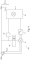
- FIG. 4 shows a block diagram of a further embodiment of the proposed power detector 100.
- the coupled inductors L 1 , L 2 provide an image current I SENSE of the load current I LOAD .
- the way the current is sensed is not restrictive, and it could be done also with a sense inductor coupled to a transformer.
- the "hard switching" first multiplier 10 implements the multiplication between the image current I SENSE of the current I LOAD and the sign(V LOAD (t)).
- the filter 11 at the output of the first multiplier 10 isolates the DC component of the signal and provides some amplification.
- An DC signal at the output of the filter 11 is proportional I LOAD * cos ⁇ .
- An output signal of the peak voltage detector 50 is proportional to V LOAD .
- the linear second multiplier 40 can be implemented either in the analog or in the digital domain.
- the biasing circuit 20 and the attenuator 30 may be combined in one single element.
- FIG. 5 shows a block diagram of a further exemplary embodiment of the proposed power detector 100.
- the first multiplier 10 (hard switching mixer) comprises capacitors Cs and FETs having been implemented with a passive switching mixer design.
- the output current of the first multiplier 10 is filtered by means of the filter 11 with a trans-impedance amplifier (TIA) 11a and converted into a voltage signal.
- TIA trans-impedance amplifier
- the linear multiplication by means of the second multiplier 40 is performed in the digital domain by means of a multiplexer 40a and an analog-to-digital converter 40b. Since both signals to be multiplied by the second multiplier 40 are DC signals, a single time multiplexed ADC is sufficient.
- Table 1 Conventional power detector with RF passive mixer in linear region
- Proposed power detector with passive mixer switching mode and peak detector Conventional peak voltage detector only 5 dBm - 15 dBm 5 dBm - 15 dBm -2 dBm - 17 dBm 3 0 1 +/- 1 dB +/- 1 dB +/- 4 dB 17.000 ⁇ m 2
- Antenna power range Line 3 ... Number of attenuator steps Line 4 ... overall precision Line 5 ... estimated silicon area Line 6 ... current consumption of the biasing circuit 20
- the proposed power detector 100 with numerical values shown in column 2 has a good tradeoff between the power detection precision and silicon area. It also leads to less electric current consumption as the biasing circuit for the mixer is simpler, it can be made for example of a basic resistive divider between V dd and the ground.
- the +/- 4 dB precision for the peak voltage detector shown in FIG. 2 is due to the VSWR variation between 1 and 2.
- the proposed power detector has a good precision of +-/ 1 dB even with a VSWR variation between 1 and 2.
- the proposed power detector 100 provides a way to implement a true power detector by removing linear multiplication of the RF-signals (current and voltage).
- the proposed power detector features a circuit that generates a replica I SENSE of the load output current I LOAD , a voltage detector, that generate a DC signal proportional to the load voltage V LOAD , and two multipliers: a first multiplier 10 that performs the multiplication between I SENSE and the sign of V LOAD , and a second multiplier 40 that performs the multiplication between the DC components of the first multiplier output, and the voltage detector output.
- a filter 11 might be needed in between the first multiplier output and the second multiplier input to extract only the DC-value of the signal and provides some amplification.
- FIG. 6 shows a principal flow of the proposed method:
- What is new in the proposed invention is to do a power detector by doing two successive multiplications : a first multiplication between I SENSE and the sign of V LOAD , and a second multiplication between the DC components of the first multiplier output, and the peak voltage detector output, instead of a single RF multiplication of voltage and current as in classical power detectors.
- the specifications for the linear multiplier are relaxed, and a digital implementation is now possible, that allow to do a very precise linear multiplication with only few digital gates, leading to a power detector with a good precision with less silicon area.
- the biasing for the RF multiplier and the optional RF attenuator are relaxed because the RF multiplier doesn't have to be linear anymore.
- the proposed power detector 100 can e.g. be used for a radio platform for Bluetooth connectivity.
- circuits or circuitry which may be illustrated as or using terms such as blocks, modules, device, system, unit, controller, etc. and/or other circuit-type depictions.
- Such circuits or circuitry are used together with other elements to exemplify how certain embodiments may be carried out in the form or structures, steps, functions, operations, activities, etc.
- the logic circuitry may correspond to logic circuitry (which may refer to or include a code-programmed/configured CPU
- the logic circuitry may carry out a process or method (sometimes "algorithm") by performing such activities and/or steps associated with the above-discussed functionalities.
- the logic circuitry may carry out a process or method by performing these same activities/operations.
- one or more modules are discrete logic circuits or programmable logic circuits configured and arranged for implementing these operations/activities.
- a programmable circuit is one or more computer circuits, including memory circuitry for storing and accessing a program to be executed as a set (or sets) of instructions (and/or to be used as configuration data to define how the programmable circuit is to perform), and an algorithm or process as described above is used by the programmable circuit to perform the related steps, functions, operations, activities, etc.
- the instructions can be configured for implementation in logic circuitry, with the instructions (whether characterized in the form of object code, firmware or software) stored in and accessible from a memory (circuit).
- the instructions whether characterized in the form of object code, firmware or software
- a memory circuit
- the adjectives "first” and “second” are not used to connote any description of the structure or to provide any substantive meaning; rather, such adjectives are merely used for English-language antecedence to differentiate one such similarly-named structure from another similarly-named structure.
- the discloses devices, apparatuses, units, elements, systems and methods described herein may at least partially be embodied by a computer program or a plurality of computer programs, which may exist in a variety of forms both active and inactive in a single computer system or across multiple computer systems.
- they may exist as software program(s) comprised of program instructions in source code, object code, executable code or other formats for performing some of the steps.
- Any of the above may be embodied on a computer readable medium, which may include storage devices and signals, in compressed or uncompressed form.
Landscapes
- Engineering & Computer Science (AREA)
- Power Engineering (AREA)
- Physics & Mathematics (AREA)
- General Physics & Mathematics (AREA)
- Measurement Of Current Or Voltage (AREA)
Abstract
- a transformer (L1, L2) configured to sense an electrical current (ILOAD) of a load (ZLOAD) and to provide an image current (ISENSE) of said electric current (ILOAD);
- a first multiplier (10) configured to perform a multiplication of the image current (ISENSE) with a sign of a voltage (VLOAD) of the load (ZLOAD) and to feed a result of said multiplication to a filter (11), the filter (11) configured to provide a DC signal;
- a peak voltage detector (50) configured to determine a peak value (S2) of the voltage (VLOAD);
- a second multiplier (40) configured to perform a linear multiplication of the output (S1) of the filter (11) with the peak value (S2); and
- a biasing circuit (20) configured to provide a biasing signal for the first multiplier (10), wherein the biasing signal is essentially independent of temperature and/or process of the first multiplier (10).
Description
- The present disclosure relates to a power detector. Furthermore, the present invention relates to a method for operating a power detector.
- In conventional electric power detector implementations, a linear multiplication of RF signals is done (current and voltage). The multiplier that does this multiplication needs to be kept linear whatever the PVT conditions in order to have a precise power measurement. Keeping the multiplier linear in PVT requires a big and complex biasing circuit. Moreover the biasing circuit output must be variable with the conditions PVT in order to keep the multiplier in its linear region. Also a variable attenuator is needed to cover the power range to be measured in order to keep the multiplier in its linear region. If all these conditions are not met, then the power measurement suffers from lack of precision and is not usable. Classical power detector implementations suffer from limited precision in PVT and when the voltage standing wave ratio (VSWR) is varied.
- V. Qunaj and P. Reynaert, "An E-band Fully-Integrated True Power Detector in 28nm CMOS", University of Leuven, 2019 IEEE Radio Frequency Integrated Circuits Symposium (RFIC), discloses a design of a power amplifier with a low-power fully-integrated E-band true power detector in a 28nm CMOS technology.
-
US 10,082,528 B2 -
US 9,686,024 B2 - It is an object of the present invention to provide an improved electric power detector.
- According to a first aspect, the present disclosure proposes a power detector, comprising:
- a transformer configured to sense an electrical current of a load and to provide an image current of said electric current;
- a first multiplier configured to perform a multiplication of the image current with a sign of a voltage of the load and to feed a result of said multiplication to a filter, the filter configured to provide a DC signal;
- a peak voltage detector configured to determine a peak value of the voltage;
- a second multiplier configured to perform a linear multiplication of the output of the filter with the peak value; and
- a biasing circuit configured to provide a biasing signal for the first multiplier, wherein the biasing signal is essentially independent of temperature and/or process of the first multiplier.
- In this way, a biasing circuit can be implemented more easier than in prior art. This is due to the fact that the first multiplier is implemented as a non-linear hard switching mixer, which means that no compensation for non-linearity of the multiplier is necessary. The second multiplier multiplies two DC signals, hence the second multiplier may be implemented easier than in prior art. As a result, a current and semiconductor area-saving design of the proposed power detector is implementable. The proposed power detector offers an improved trade-off between precision and area.
- According to a further aspect, the present disclosure proposes a method for operating a power detector, comprising the steps:
- sensing an electrical current of a load and providing an image current of said electric current;
- performing a multiplication of the image current with a sign of a voltage of the load;
- feeding the result of said multiplication to a filter, the filter configured to provide a DC signal;
- determining a peak value of the voltage;
- performing a linear multiplication of the output of the filter with the peak value; and
- providing a biasing signal for the first multiplier during the measurement of the electric power of the load, wherein the biasing signal is essentially independent of temperature and/or process of the first multiplier.
- In one or more embodiments, an output signal of the filter represents a multiplication of the image current by the cosine of a phase difference between the load current and the load voltage.
- In one or more embodiments, the biasing circuit is one of the following: constant current source, voltage source of a bandgap.
- In one or more embodiments, the power detector further comprises an attenuator configured to adapt a working range of the first multiplier. In this way, the existence of the attenuator depends on a range which is intended to be measured. If the power is too great and to prevent damage of components of the first multiplier, the attenuator may be required.
- According to one or more embodiments, the attenuator is programmable.
- According to one or more embodiments, the second multiplier is a digital multiplier. The linear multiplication of the output of the peak voltage detector and the filter is done in the digital world due to static input signals to the second multiplier.
- According to one or more embodiments the second multiplier is an analog multiplier.
- According to one or more embodiments the biasing circuit and the attenuator are implemented in one single element.
- According to one or more embodiments the first multiplier corresponds to a Heaviside function of the voltage instead of the sign function.
- Various example embodiments may be more completely understood in consideration of the following detailed description in connection with the accompanying drawings, in which:
- FIG. 1
- shows a block diagram of the conventional power detector;
- FIG. 2
- shows a block diagram of a further conventional power detector;
- FIG. 3
- shows a block diagram of an embodiment of a proposed power detector;
- FIG. 4
- shows a block diagram of a further embodiment of the proposed power detector;
- FIG. 5
- shows a block diagram of a further embodiment of the proposed power detector; and
- FIG. 6
- is a diagram showing a flow of a proposed method of operating a power detector.
- The above discussion/summary is not intended to describe each embodiment or every implementation of the present disclosure. The drawings and detailed description that follow also exemplify various embodiments. The aspects defined above and further aspects of the present disclosure are apparent from the examples of embodiment to be described hereinafter with reference to the appended drawings, which are explained with reference to the examples of embodiment. Needless to say, that the disclosure is not limited to the examples of embodiments.
- All illustrations in the drawings are schematical. It is noted that in different figures, similar or identical elements or features are provided with the same reference signs or with reference signs that are different from the corresponding reference signs only within the first digit. In order to avoid unnecessary repetitions, elements or features which have already been elucidated with respect to a previously described embodiment are not elucidated again at a later position of the description.
-
FIG. 1 shows a block diagram of a conventionalelectric power detector 100 for measuring electric power of a load ZLOAD. Basically, said power is measured by a multiplication of an image current ISENSE of an electric current ILOAD and an electric voltage VLOAD of the load ZLOAD. The voltage VLOAD is sensed by anattenuator 30 and is fed to afirst multiplier 10. One recognizes a transformer having two inductors L1, L2 with a transfer factor k, which senses an image current ISENSE, which is fed to thefirst multiplier 10. Thefirst multiplier 10 performs a multiplication of the image current ISENSE with the voltage VLOAD and may be somewhat sensitive to variations of temperature and process variations. That is, thefirst multiplier 10 performs a linear multiplication of RF signals. - To this end, the
first multiplier 10 needs to be biased by means of biasing signals of a biasingcircuit 20 in order to keep operating characteristics of thefirst multiplier 10 as linear as possible. In addition, anattenuator 30 is provided, which adjusts a suitable working range for thefirst multiplier 10. An output of thefirst multiplier 10 is filtered by afilter 11 in order to provide a DC signal. Said DC signal is an image of the electric power P of the load ZLOAD. - As the value of the output of the
first multiplier 10 is important, it is important that thefirst multiplier 10 has linear characteristics. Theattenuator 30 is needed because a certain range of the power P in the load ZLOAD is measured, in order to hold the input of thefirst multiplier 10 quite constant within a given power range. This is indicated with a sub diagram near theattenuator 30 showing exemplary attenuation steps of a programmable step attenuator over power. - The biasing
circuit 20 needs to follow a behavior of thefirst multiplier 10 in terms of temperature and process, in order to keep thefirst multiplier 10 in its linear region, which is indicated in two exemplary sub diagrams next to the biasingcircuit 20. The biasingcircuit 20 can be e.g. a current source or a voltage regulator. The linearfirst multiplier 10 is done in analog way with transistors and a transfer function of thefirst multiplier 10 is not linear over temperature and process, therefore its output does not exactly represent a multiplication of both inputs, when the temperature and/or the process changes. Said biasingcircuit 20 needs to be precise in order to keep the linearfirst multiplier 10 in its linear region, which requires great semiconductor area. Moreover, the biasingcircuit 20 needs a variable output signal versus PVT, which may results in a rather complex implementation of the biasingcircuit 20. - A measurement of the RMS power PLOAD in the load ZLOAD at the frequency ω/2p can be done in the following way:


- VL
- peak value of load voltage
- IL
- peak value of load current
- φ
- phase between load voltage and load current
- The RMS power PLOAD can be evaluated by linearly multiplying ILOAD and VLOAD and taking the DC term of the multiplied signal:


- This method requires an
analog RF multiplier 10 that perform the linear time multiplication between the two RF signals. Such multiplier is difficult to implements over a wide range of PLOAD and over process, voltage, and temperature variation (PVT). -
FIG. 2 shows a detail of a conventional implementation of a power detector that uses avoltage peak detector 50. In effect, this represents an example of a power detector that is done only with apeak detector 50. The RMS power can also be measured with apeak voltage detector 50 only in case the impedance of the load ZLOAD is well known, for example 50 Ohms fixed. An output signal of thepeak voltage detector 50 is proportional to VLOAD and is fed to anADC 51, which outputs a signal being representative of the power P. - In case the load impedance ZLOAD is purely resistive (e.g. 50 Ohms), the RMS power is obtained from the VLOAD information from the
peak voltage detector 50 as follows:
- The voltage VLOAD and the current ILOAD are in phase in this case, which results in a kind of pure voltage detector. However, a problem in this case may be, that if the load impedance varies, then the power measured through the
peak voltage detector 50 only is no more accurate. -
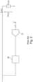
FIG. 3 is a block diagram of a first embodiment of the proposedpower detector 100. One recognizes the transformer having two inductors L1, L2 with a transmission factor k provides an image ISENSE of the current ILOAD and the biasingcircuit 20. Differing from the conventional arrangement shown inFIG. 1 , afirst multiplier 10 uses the image current ISENSE and furthermore uses a phase relationship with a phase φ between the current ILOAD and the voltage VLOAD. The cosine φ is a phase relation between current ILOAD and voltage VLOAD of the load ZLOAD. The first multiplier performs a multiplication of the image current ISENSE and a sign of the relationship and provides said image to afilter 11, which provides a DC signal S1 and feeds said DC signal S1 to asecond multiplier 40. Thefirst multiplier 10 is implemented as a non-linear hard switching mixer, which means that the mixer does not do a multiplication of the two inputs, rather one of its inputs has a very high amplitude in order to do a switching operation and it is essentially non-linear. - In effect, the
first multiplier 10 has a non-linear transfer function, which means, that thefirst multiplier 10 is used as a limiter. As a result, thefirst multiplier 10 is used as a hard switching mixer. Only a characteristic of edges (rising or falling edge) of the input signal (VOUT) is determined, such that the phase relationship of input signals is known. At the output of the first multiplier 10 a signal is provided, wherein such signal represents the multiplication of the image of the current ISENSE with the phase of the output voltage VOUT. - The
attenuator 30 may be optional, depending on a range which is intended to be detected, in order to protect components of thefirst multiplier 10 from damage. In case, that the output of thefirst multiplier 10 is not too strong, theattenuator 30 is not required. The output S1 of thefilter 11 removes the high frequency component of the first multiplier output signal, leaving only the DC component. Its output signal S1 represents the multiplication of the image of the current ISENSE by the cosine of the phase difference between the load current (ILOAD) and the load voltage (VOUT). - In addition to the load current and the phase information between load current and load voltage, also an information regards the load voltage amplitude is needed. To this end, a
peak voltage detector 50 is used, which is much easier to be implemented than a power detector. An output signal S2 of amaximum peak detector 50 represents a peak value of the voltage VLOAD. Both signals S1, S2 are DC signals so they can be multiplied by thelinear multiplier 40 via a linear multiplication in analog or in digital. - One recognizes a biasing
circuit 20 being functionally connected with thefirst multiplier 10 and a biasing signal diagram, with a biasing signal being essentially independent of process and temperature. This allows a much more easier implementation of the biasingcircuit 20. For example, the biasingcircuit 20 can be implemented as a constant current source, voltage source from a bandgap, etc. - An
optional attenuator 30 is provided in a case, that an operation range has to be adjusted for thefirst multiplier 10. Alternatively, the biasingcircuit 20 and theattenuation circuit 50 can be implemented in one single element. Also, theattenuator 30 can be implemented as a programmable unit. - As a result, in the proposed
power detector 100 the linear multiplier of the two RF signal as performed in the arrangement ofFIG. 1 is replaced by twomultipliers voltage peak detector 50. That means a hard switching RF multiplier is provided to retrieve a phase relationship between the RF current and the voltage of the load together with a linearsecond multiplier 40, whose input signals S1, S2 are DC-signals. Resulting therefrom, a muchrelaxed biasing circuit 20 for theRF multiplier 10 is implementable, since doesn't have to operate in linear region anymore. For the same power range to be covered theattenuator 30 may be simpler and might even be removed. The linear multiplication of thesecond multiplier 40 is performed between DC signals, which is much easier to implement and can be done in digital (after ADC conversion) or in analog. - The same results can be achieved by multiplying ILOAD by the sign of VLOAD, taking the DC value of the multiplication, and multiplying such DC value by the peak value of VLOAD in the following way:


peak voltage detector 50.
- In the proposed
power detector 100 the hard switching mixer of the first multiplier10 may correspond to a Heaviside function of VLOAD, instead of the sign function, thus a factor of two must be applied. - An advantage of the proposed
power detector 100 and its performed method of power detection is that the required linear multiplication is now applied to two DC signals, and is then much easier to implement (either in analog or digital). The first multiplication still require to multiply two RF signals, but it can be implemented as a hard-switching multiplier, that is much easier to implement over a wide range of PLOAD and PVT. - Resulting therefrom, the proposed
power detector 100 is easier to be implemented than in a conventional way and allows a current saving and/or area saving implementation of the power detector. -
FIG. 4 shows a block diagram of a further embodiment of the proposedpower detector 100. The coupled inductors L1, L2 provide an image current ISENSE of the load current ILOAD. The way the current is sensed is not restrictive, and it could be done also with a sense inductor coupled to a transformer. - The "hard switching"
first multiplier 10 implements the multiplication between the image current ISENSE of the current ILOAD and the sign(VLOAD(t)). Thefilter 11 at the output of thefirst multiplier 10 isolates the DC component of the signal and provides some amplification. An DC signal at the output of thefilter 11 is proportional ILOAD * cos φ. An output signal of thepeak voltage detector 50 is proportional to VLOAD. - Also in this case, the linear
second multiplier 40 can be implemented either in the analog or in the digital domain. One recognizes, that the biasingcircuit 20 and theattenuator 30 may be combined in one single element. -
FIG. 5 shows a block diagram of a further exemplary embodiment of the proposedpower detector 100. In this implementation the first multiplier 10 (hard switching mixer) comprises capacitors Cs and FETs having been implemented with a passive switching mixer design. The output current of thefirst multiplier 10 is filtered by means of thefilter 11 with a trans-impedance amplifier (TIA) 11a and converted into a voltage signal. The linear multiplication by means of thesecond multiplier 40 is performed in the digital domain by means of amultiplexer 40a and an analog-to-digital converter 40b. Since both signals to be multiplied by thesecond multiplier 40 are DC signals, a single time multiplexed ADC is sufficient. - Most of today IC already contains a general-purpose ADC anyway. In this case the digital linear multiplication does not require any additional hardware other than the actual multiplier (few digital gates).
- The following table shows numerical values of different power detectors as explained in the foregoing:
Table 1 Conventional power detector with RF passive mixer in linear region Proposed power detector with passive mixer switching mode and peak detector Conventional peak voltage detector only 5 dBm - 15 dBm 5 dBm - 15 dBm -2 dBm - 17 dBm 3 0 1 +/- 1 dB +/- 1 dB +/- 4 dB 17.000 µm2 4.500 µm2 1.000 µm 2100 µA 10 µA - Line 2 ... Antenna power range
Line 3 ... Number of attenuator steps
Line 4 ... overall precision
Line 5 ... estimated silicon area
Line 6 ... current consumption of the biasingcircuit 20 - As can be seen from table 1, the proposed
power detector 100 with numerical values shown in column 2 has a good tradeoff between the power detection precision and silicon area. It also leads to less electric current consumption as the biasing circuit for the mixer is simpler, it can be made for example of a basic resistive divider between Vdd and the ground. - The +/- 4 dB precision for the peak voltage detector shown in
FIG. 2 is due to the VSWR variation between 1 and 2. The proposed power detector has a good precision of +-/ 1 dB even with a VSWR variation between 1 and 2. - The proposed
power detector 100 provides a way to implement a true power detector by removing linear multiplication of the RF-signals (current and voltage). The proposed power detector features a circuit that generates a replica ISENSE of the load output current ILOAD, a voltage detector, that generate a DC signal proportional to the load voltage VLOAD, and two multipliers: afirst multiplier 10 that performs the multiplication between ISENSE and the sign of VLOAD, and asecond multiplier 40 that performs the multiplication between the DC components of the first multiplier output, and the voltage detector output. - A
filter 11 might be needed in between the first multiplier output and the second multiplier input to extract only the DC-value of the signal and provides some amplification. - One recognizes that only the
second multiplier 40 performs a linear multiplication. Due to the fact that it multiplies two DC signals, it is much easier to implements compared to prior art, where thelinear multiplier 10 multiplies two RF signals. -
FIG. 6 shows a principal flow of the proposed method: - In a
step 200, a an electrical current ILOAD of a load ZLOAD is sensed and an image current ISENSE of said electric current ILOAD is provided. - In a step 210 a multiplication of the image current ISENSE with a sign of a voltage VLOAD of the load ZLOAD is performed.
- In a
step 220 the result of said multiplication is fed to afilter 11, thefilter 11 configured to provide a DC signal. - In a step 230 a peak value S2 of the voltage VLOAD is determined.
- In a step 240 a linear multiplication of the output S1 of the
filter 11 with the peak value S2 is performed. - In a step 250 a biasing signal for the
first multiplier 10 during the measurement of the electric power of the load ZLOAD is provided, wherein the biasing signal is essentially independent of temperature and/or process of thefirst multiplier 10. - All mentioned numerical values are only exemplary and can be exchanged with alternative suitable numerical values. Also, the disclosed numerical values are to be understood in a qualitative sense and are represented in a standardized form.
- What is new in the proposed invention is to do a power detector by doing two successive multiplications : a first multiplication between ISENSE and the sign of VLOAD, and a second multiplication between the DC components of the first multiplier output, and the peak voltage detector output, instead of a single RF multiplication of voltage and current as in classical power detectors. The specifications for the linear multiplier are relaxed, and a digital implementation is now possible, that allow to do a very precise linear multiplication with only few digital gates, leading to a power detector with a good precision with less silicon area. The biasing for the RF multiplier and the optional RF attenuator are relaxed because the RF multiplier doesn't have to be linear anymore.
- The proposed
power detector 100 can e.g. be used for a radio platform for Bluetooth connectivity. - In the foregoing description various specific details have been set forth to describe specific examples presented herein. It should be apparent to one skilled in the art, however, that one or more other examples and/or variations of these examples may be practiced without all the specific details given below. In other instances, well known features have not been described in detail so as not to obscure the description of the examples herein. For ease of illustration, the same reference signs may be used in different diagrams to refer to the same elements or additional instances of the same element. Also, although aspects and features may in some cases be described in individual figures, it will be appreciated that features from one figure or embodiment can be combined with features of another figure or embodiment even though the combination is not explicitly shown or explicitly described as a combination.
- As examples, the specification describes and/or illustrates aspects useful for implementing the claimed disclosure by way of various circuits or circuitry which may be illustrated as or using terms such as blocks, modules, device, system, unit, controller, etc. and/or other circuit-type depictions. Such circuits or circuitry are used together with other elements to exemplify how certain embodiments may be carried out in the form or structures, steps, functions, operations, activities, etc. As examples, wherein such circuits or circuitry may correspond to logic circuitry (which may refer to or include a code-programmed/configured CPU, in one example the logic circuitry may carry out a process or method (sometimes "algorithm") by performing such activities and/or steps associated with the above-discussed functionalities. In other examples, the logic circuitry may carry out a process or method by performing these same activities/operations.
- For example, in certain of the above-discussed embodiments, one or more modules are discrete logic circuits or programmable logic circuits configured and arranged for implementing these operations/activities. In certain embodiments, such a programmable circuit is one or more computer circuits, including memory circuitry for storing and accessing a program to be executed as a set (or sets) of instructions (and/or to be used as configuration data to define how the programmable circuit is to perform), and an algorithm or process as described above is used by the programmable circuit to perform the related steps, functions, operations, activities, etc. Depending on the application, the instructions (and/or configuration data) can be configured for implementation in logic circuitry, with the instructions (whether characterized in the form of object code, firmware or software) stored in and accessible from a memory (circuit). As another example, where the specification may make reference to a "first" type of structure, a "second" type of structure, where the adjectives "first" and "second" are not used to connote any description of the structure or to provide any substantive meaning; rather, such adjectives are merely used for English-language antecedence to differentiate one such similarly-named structure from another similarly-named structure.
- Based upon the above discussion and illustrations, those skilled in the art will readily recognize, that various modifications and changes may be made to the various embodiments without strictly following the exemplary embodiments and applications illustrated and described herein. For example, methods as exemplified in the Figures may involve steps carried out in various orders, with one or more aspects of the embodiments herein retained, or may involve fewer or more steps.
- While various embodiments discussed herein are amenable to modifications and alternative forms, aspects thereof have been shown by way of example in the drawings and will be described in detail. It should be understood, however, that the intention is not to limit the disclosure to the particular embodiments described. On the contrary, the intention is to cover all modifications, equivalents, and alternatives falling within the scope of the disclosure including aspects defined in the claims. In addition, the term "example" as used throughout this application is only by way of illustration, and not limitation.
- It should be noted that the term "comprising" does not exclude other elements or steps and "a" or "an" does not exclude a plurality. Also elements described in association with different embodiments may be combined. It should also be noted, that reference signs in the claims should not be construed as limiting the scope of the claims.
- The discloses devices, apparatuses, units, elements, systems and methods described herein may at least partially be embodied by a computer program or a plurality of computer programs, which may exist in a variety of forms both active and inactive in a single computer system or across multiple computer systems. For example, they may exist as software program(s) comprised of program instructions in source code, object code, executable code or other formats for performing some of the steps. Any of the above may be embodied on a computer readable medium, which may include storage devices and signals, in compressed or uncompressed form.
- It is noted that the embodiments above have been described with reference to different subject-matters. In particular, some embodiments may have been described with reference to method-type claims whereas other embodiments may have been described with reference to apparatus-type claims.
- However, a person skilled in the art will gather from the above that, unless otherwise indicated, in addition to any combination of features belonging to one type of subject-matter also any combination of features relating to different subject-matters, in particular a combination of features of the method-type claims and features of the apparatus-type claims, is considered to be disclosed with this document.
- It has to be noted that embodiments have been described with reference to different subject matters. In particular, some embodiments have been described with reference to method type claims whereas other embodiments have been described with reference to apparatus type claims.
- However, a person skilled in the art will gather from the above description that, unless other notified, in addition to any combination of features belonging to one type of subject matter also any combination between features relating to different subject matters, in particular between features of the method type claims and features of the apparatus type claims is considered as to be disclosed with this application.
-
- 10
- first multiplier
- 11
- filter
- 20
- biasing circuit
- 30
- attenuator
- 40
- second multiplier
- 40a
- multiplexer
- 40b
- ADC
- 50
- voltage peak detector
- 51
- ADC
- 100
- power detector
- 200...250
- method steps
- L1, L2
- inductor
- ILOAD
- load current
- ISENSE
- image current
- VLOAD
- load voltage
- Z
- load
Claims (13)
- Power detector (100), comprising:- a transformer (L1, L2) configured to sense an electrical current (ILOAD) of a load (ZLOAD) and to provide an image current (ISENSE) of said electric current (ILOAD);- a first multiplier (10) configured to perform a multiplication of the image current (ISENSE) with a sign of a voltage (VLOAD) of the load (ZLOAD) and to feed a result of said multiplication to a filter (11), the filter (11) configured to provide a DC signal;- a peak voltage detector (50) configured to determine a peak value (S2) of the voltage (VLOAD);- a second multiplier (40) configured to perform a linear multiplication of the output (S1) of the filter (11) with the peak value (S2); and- a biasing circuit (20) configured to provide a biasing signal for the first multiplier (10), wherein the biasing signal is essentially independent of temperature and/or process of the first multiplier (10).
- Power detector (100) according to claim 1, wherein an output signal (S1) of the filter (11) represents a multiplication of the image current (ISENSE) by the cosine of a phase difference between the load current (ILOAD) and the load voltage (VOUT).
- Power detector (100) according to claim 1 or 2, wherein the biasing circuit (20) is one of the following: constant current source, voltage source of a bandgap.
- Power detector (100) according to any of the preceding claims, further comprising an attenuator (30) configured to adapt a working range of the first multiplier (10).
- Power detector (100) according to claim 4, wherein the attenuator (30) is programmable.
- Power detector (100) according to any of the preceding claims, wherein the second multiplier (40) is a digital multiplier.
- Power detector (100) according to any of claims 1 to 5, wherein the second multiplier (40) is an analog multiplier.
- Power detector (100) according to any of the preceding claims, wherein the biasing circuit (20) and the attenuator (30) are implemented in one single element.
- Power detector (100) according to any of the preceding claims, wherein the first multiplier (10) corresponds to a Heaviside function of the voltage (VLOAD) instead of the sign function.
- Method for providing a measurement of electric power of a load (ZLOAD), comprising the steps:- sensing an electrical current (ILOAD) of a load (ZLOAD) and providing an image current (ISENSE) of said electric current (ILOAD);- performing a multiplication of the image current (ISENSE) with a sign of a voltage (VLOAD) of the load (ZLOAD)- feeding the result of said multiplication to a filter (11), the filter (11) configured to provide a DC signal;- determining a peak value (S2) of the voltage (VLOAD);- performing a linear multiplication of the output (S1) of the filter (11) with the peak value (S2); and- providing a biasing signal for the first multiplier (10) during the measurement of the electric power of the load (ZLOAD), wherein the biasing signal is essentially independent of temperature and/or process of the first multiplier (10).
- Method according to claim 10, wherein the linear multiplication of the output (S1) of the filter (11) with the peak value (S2) is done in digital.
- Method according to claim 10, wherein the linear multiplication of the output (S1) of the filter (11) with the peak value (S2) is done in analog.
- Method according to any of the claims 10 to 12, further comprising an adaptation of a working range of the first multiplier (10).
Priority Applications (3)
| Application Number | Priority Date | Filing Date | Title |
|---|---|---|---|
| EP23307147.1A EP4567435A1 (en) | 2023-12-06 | 2023-12-06 | Power detector and method for operating a power detector |
| US18/937,507 US20250189565A1 (en) | 2023-12-06 | 2024-11-05 | Power detector and method for operating a power detector |
| CN202411725372.0A CN120102966A (en) | 2023-12-06 | 2024-11-28 | Power detector and method for operating a power detector |
Applications Claiming Priority (1)
| Application Number | Priority Date | Filing Date | Title |
|---|---|---|---|
| EP23307147.1A EP4567435A1 (en) | 2023-12-06 | 2023-12-06 | Power detector and method for operating a power detector |
Publications (1)
| Publication Number | Publication Date |
|---|---|
| EP4567435A1 true EP4567435A1 (en) | 2025-06-11 |
Family
ID=89385980
Family Applications (1)
| Application Number | Title | Priority Date | Filing Date |
|---|---|---|---|
| EP23307147.1A Pending EP4567435A1 (en) | 2023-12-06 | 2023-12-06 | Power detector and method for operating a power detector |
Country Status (3)
| Country | Link |
|---|---|
| US (1) | US20250189565A1 (en) |
| EP (1) | EP4567435A1 (en) |
| CN (1) | CN120102966A (en) |
Citations (5)
| Publication number | Priority date | Publication date | Assignee | Title |
|---|---|---|---|---|
| US3764908A (en) * | 1972-03-06 | 1973-10-09 | Westinghouse Electric Corp | Electronic wattmeter including a solid-state logarithmic multiplier |
| US4788494A (en) * | 1985-01-09 | 1988-11-29 | Refac Electronics Corporation | Power measuring apparatus |
| US9686024B2 (en) | 2015-04-27 | 2017-06-20 | Avago Technologies General Ip (Singapore) Pte. Ltd. | True radio frequency (RF) power detector |
| US10082528B2 (en) | 2015-05-13 | 2018-09-25 | Mediatek Inc. | Power detector |
| US20220091167A1 (en) * | 2019-01-29 | 2022-03-24 | Sentec Ltd | Electricity meter |
-
2023
- 2023-12-06 EP EP23307147.1A patent/EP4567435A1/en active Pending
-
2024
- 2024-11-05 US US18/937,507 patent/US20250189565A1/en active Pending
- 2024-11-28 CN CN202411725372.0A patent/CN120102966A/en active Pending
Patent Citations (5)
| Publication number | Priority date | Publication date | Assignee | Title |
|---|---|---|---|---|
| US3764908A (en) * | 1972-03-06 | 1973-10-09 | Westinghouse Electric Corp | Electronic wattmeter including a solid-state logarithmic multiplier |
| US4788494A (en) * | 1985-01-09 | 1988-11-29 | Refac Electronics Corporation | Power measuring apparatus |
| US9686024B2 (en) | 2015-04-27 | 2017-06-20 | Avago Technologies General Ip (Singapore) Pte. Ltd. | True radio frequency (RF) power detector |
| US10082528B2 (en) | 2015-05-13 | 2018-09-25 | Mediatek Inc. | Power detector |
| US20220091167A1 (en) * | 2019-01-29 | 2022-03-24 | Sentec Ltd | Electricity meter |
Non-Patent Citations (1)
| Title |
|---|
| V. QUNAJP. REYNAERT: "IEEE Radio Frequency Integrated Circuits Symposium (RFIC", 2019, UNIVERSITY OF LEUVEN, article "An E-band Fully-Integrated True Power Detector in 28nm CMOS" |
Also Published As
| Publication number | Publication date |
|---|---|
| US20250189565A1 (en) | 2025-06-12 |
| CN120102966A (en) | 2025-06-06 |
Similar Documents
| Publication | Publication Date | Title |
|---|---|---|
| TW546835B (en) | Integrated power detector with temperature compensation | |
| US8306489B2 (en) | Circuit for a loop antenna and method for tuning | |
| Irwin et al. | Microwave SQUID multiplexer | |
| EP1800410B1 (en) | Impedance detector | |
| US9292716B2 (en) | Method and apparatus for detecting an output power of a radio frequency transmitter using a multiplier circuit | |
| US7974598B2 (en) | Methods and apparatus for calibrating received signal strength indicators | |
| US8319549B2 (en) | Self-healing power amplifier: methods and apparatus | |
| CN104335485B (en) | power detector with temperature compensation | |
| EP0398712A2 (en) | An amplification circuit | |
| CN106324336A (en) | Power detection circuit, power amplifier module and power calibration circuit | |
| US20120316817A1 (en) | Measurement circuit for measuring direct current resistance of inductor | |
| CN113640576A (en) | Radio frequency power detection circuit and electronic equipment | |
| US8022688B2 (en) | RF power detector | |
| Oezdamar et al. | An RF voltage detector with low harmonic feedback for antenna tuning switches | |
| US10082528B2 (en) | Power detector | |
| US20250189565A1 (en) | Power detector and method for operating a power detector | |
| US20070030064A1 (en) | Integrated laterally diffused metal oxide semiconductor power detector | |
| CN103063949B (en) | A kind of capacitor mismatch detection circuit and method | |
| US6335651B1 (en) | Low voltage mixer | |
| US11223329B2 (en) | Stacked segmented power amplifier circuitry and a method for controlling a stacked segmented power amplifier circuitry | |
| US6545541B2 (en) | Power amplifier embedded cell bias detection, methods of detecting bias in power amplifiers and systems utilizing embedded cell bias detection | |
| US8331882B1 (en) | VSWR normalizing envelope modulator | |
| Solomko et al. | Successive approximation RF reflectometer for antenna tuning in cellular handheld devices | |
| US6534966B2 (en) | Methods and apparatus for power measuring receiver | |
| EP3364198B1 (en) | Apparatus for detecting current |
Legal Events
| Date | Code | Title | Description |
|---|---|---|---|
| PUAI | Public reference made under article 153(3) epc to a published international application that has entered the european phase |
Free format text: ORIGINAL CODE: 0009012 |
|
| STAA | Information on the status of an ep patent application or granted ep patent |
Free format text: STATUS: THE APPLICATION HAS BEEN PUBLISHED |
|
| AK | Designated contracting states |
Kind code of ref document: A1 Designated state(s): AL AT BE BG CH CY CZ DE DK EE ES FI FR GB GR HR HU IE IS IT LI LT LU LV MC ME MK MT NL NO PL PT RO RS SE SI SK SM TR |
|
| STAA | Information on the status of an ep patent application or granted ep patent |
Free format text: STATUS: REQUEST FOR EXAMINATION WAS MADE |
|
| 17P | Request for examination filed |
Effective date: 20251211 |
|
| GRAP | Despatch of communication of intention to grant a patent |
Free format text: ORIGINAL CODE: EPIDOSNIGR1 |
|
| STAA | Information on the status of an ep patent application or granted ep patent |
Free format text: STATUS: GRANT OF PATENT IS INTENDED |
|
| RIC1 | Information provided on ipc code assigned before grant |
Ipc: G01R 21/06 20060101AFI20260604BHEP Ipc: G01R 21/07 20060101ALN20260604BHEP |
|
| INTG | Intention to grant announced |
Effective date: 20260618 |