EP4564419A2 - Power module - Google Patents
Power module Download PDFInfo
- Publication number
- EP4564419A2 EP4564419A2 EP24212450.1A EP24212450A EP4564419A2 EP 4564419 A2 EP4564419 A2 EP 4564419A2 EP 24212450 A EP24212450 A EP 24212450A EP 4564419 A2 EP4564419 A2 EP 4564419A2
- Authority
- EP
- European Patent Office
- Prior art keywords
- separating
- power module
- axis
- separating element
- separating elements
- Prior art date
- Legal status (The legal status is an assumption and is not a legal conclusion. Google has not performed a legal analysis and makes no representation as to the accuracy of the status listed.)
- Pending
Links
Images








Classifications
-
- H—ELECTRICITY
- H10—SEMICONDUCTOR DEVICES; ELECTRIC SOLID-STATE DEVICES NOT OTHERWISE PROVIDED FOR
- H10W—GENERIC PACKAGES, INTERCONNECTIONS, CONNECTORS OR OTHER CONSTRUCTIONAL DETAILS OF DEVICES COVERED BY CLASS H10
- H10W76/00—Containers; Fillings or auxiliary members therefor; Seals
- H10W76/10—Containers or parts thereof
- H10W76/12—Containers or parts thereof characterised by their shape
- H10W76/13—Containers comprising a conductive base serving as an interconnection
- H10W76/136—Containers comprising a conductive base serving as an interconnection having other interconnections perpendicular to the conductive base
-
- H—ELECTRICITY
- H10—SEMICONDUCTOR DEVICES; ELECTRIC SOLID-STATE DEVICES NOT OTHERWISE PROVIDED FOR
- H10W—GENERIC PACKAGES, INTERCONNECTIONS, CONNECTORS OR OTHER CONSTRUCTIONAL DETAILS OF DEVICES COVERED BY CLASS H10
- H10W40/00—Arrangements for thermal protection or thermal control
- H10W40/20—Arrangements for cooling
- H10W40/25—Arrangements for cooling characterised by their materials
- H10W40/255—Arrangements for cooling characterised by their materials having a laminate or multilayered structure, e.g. direct bond copper [DBC] ceramic substrates
-
- H—ELECTRICITY
- H10—SEMICONDUCTOR DEVICES; ELECTRIC SOLID-STATE DEVICES NOT OTHERWISE PROVIDED FOR
- H10W—GENERIC PACKAGES, INTERCONNECTIONS, CONNECTORS OR OTHER CONSTRUCTIONAL DETAILS OF DEVICES COVERED BY CLASS H10
- H10W42/00—Arrangements for protection of devices
- H10W42/121—Arrangements for protection of devices protecting against mechanical damage
-
- H—ELECTRICITY
- H10—SEMICONDUCTOR DEVICES; ELECTRIC SOLID-STATE DEVICES NOT OTHERWISE PROVIDED FOR
- H10W—GENERIC PACKAGES, INTERCONNECTIONS, CONNECTORS OR OTHER CONSTRUCTIONAL DETAILS OF DEVICES COVERED BY CLASS H10
- H10W70/00—Package substrates; Interposers; Redistribution layers [RDL]
- H10W70/60—Insulating or insulated package substrates; Interposers; Redistribution layers
- H10W70/611—Insulating or insulated package substrates; Interposers; Redistribution layers for connecting multiple chips together
-
- H—ELECTRICITY
- H10—SEMICONDUCTOR DEVICES; ELECTRIC SOLID-STATE DEVICES NOT OTHERWISE PROVIDED FOR
- H10W—GENERIC PACKAGES, INTERCONNECTIONS, CONNECTORS OR OTHER CONSTRUCTIONAL DETAILS OF DEVICES COVERED BY CLASS H10
- H10W70/00—Package substrates; Interposers; Redistribution layers [RDL]
- H10W70/60—Insulating or insulated package substrates; Interposers; Redistribution layers
- H10W70/62—Insulating or insulated package substrates; Interposers; Redistribution layers characterised by their interconnections
- H10W70/65—Shapes or dispositions of interconnections
- H10W70/658—Shapes or dispositions of interconnections for devices provided for in groups H10D8/00 - H10D48/00
-
- H—ELECTRICITY
- H10—SEMICONDUCTOR DEVICES; ELECTRIC SOLID-STATE DEVICES NOT OTHERWISE PROVIDED FOR
- H10W—GENERIC PACKAGES, INTERCONNECTIONS, CONNECTORS OR OTHER CONSTRUCTIONAL DETAILS OF DEVICES COVERED BY CLASS H10
- H10W70/00—Package substrates; Interposers; Redistribution layers [RDL]
- H10W70/60—Insulating or insulated package substrates; Interposers; Redistribution layers
- H10W70/67—Insulating or insulated package substrates; Interposers; Redistribution layers characterised by their insulating layers or insulating parts
- H10W70/68—Shapes or dispositions thereof
- H10W70/685—Shapes or dispositions thereof comprising multiple insulating layers
-
- H—ELECTRICITY
- H10—SEMICONDUCTOR DEVICES; ELECTRIC SOLID-STATE DEVICES NOT OTHERWISE PROVIDED FOR
- H10W—GENERIC PACKAGES, INTERCONNECTIONS, CONNECTORS OR OTHER CONSTRUCTIONAL DETAILS OF DEVICES COVERED BY CLASS H10
- H10W74/00—Encapsulations, e.g. protective coatings
- H10W74/10—Encapsulations, e.g. protective coatings characterised by their shape or disposition
- H10W74/111—Encapsulations, e.g. protective coatings characterised by their shape or disposition the semiconductor body being completely enclosed
-
- H—ELECTRICITY
- H10—SEMICONDUCTOR DEVICES; ELECTRIC SOLID-STATE DEVICES NOT OTHERWISE PROVIDED FOR
- H10W—GENERIC PACKAGES, INTERCONNECTIONS, CONNECTORS OR OTHER CONSTRUCTIONAL DETAILS OF DEVICES COVERED BY CLASS H10
- H10W90/00—Package configurations
-
- H—ELECTRICITY
- H10—SEMICONDUCTOR DEVICES; ELECTRIC SOLID-STATE DEVICES NOT OTHERWISE PROVIDED FOR
- H10W—GENERIC PACKAGES, INTERCONNECTIONS, CONNECTORS OR OTHER CONSTRUCTIONAL DETAILS OF DEVICES COVERED BY CLASS H10
- H10W90/00—Package configurations
- H10W90/701—Package configurations characterised by the relative positions of pads or connectors relative to package parts
-
- H—ELECTRICITY
- H10—SEMICONDUCTOR DEVICES; ELECTRIC SOLID-STATE DEVICES NOT OTHERWISE PROVIDED FOR
- H10W—GENERIC PACKAGES, INTERCONNECTIONS, CONNECTORS OR OTHER CONSTRUCTIONAL DETAILS OF DEVICES COVERED BY CLASS H10
- H10W74/00—Encapsulations, e.g. protective coatings
Definitions
- the present disclosure relates to a power module, and in particular it relates to a power module that can reduce the volume.
- a power module has a plurality of pins for signal transmission.
- the distance between adjacent pins is limited, making it very hard to reduce the overall size of the power module.
- one objective of the present disclosure is to provide a power module to solve the above problems.
- a power module includes a substrate, a semiconductor component, a plurality of pins and a package body.
- the substrate has a first metal surface.
- the semiconductor component is disposed on the first metal surface.
- the plurality of pins extend from the first metal surface and are configured to be electrically connected to the semiconductor component.
- the package body is configured to cover the first metal surface and the semiconductor component, and the package body partially encloses each of the pins. There is a gap between each two adjacent pins, and a separating element is disposed in each gap to increase the creepage distance between two adjacent pins.
- the plurality of pins extends along a first axis, and when viewed along the first axis, the plurality of pins are arranged in a matrix.
- the separating elements when viewed along the first axis, include a plurality of first separating elements, each of the first separating elements has a strip-shaped structure which extends along a second axis, and the second axis is perpendicular to the first axis.
- the separating elements when viewed along the first axis, the separating elements further include a plurality of second separating elements, each of the second separating elements has a strip-shaped structure which extends along a third axis, and the third axis is perpendicular to the first axis and the second axis.
- the first separating elements are connected to the second separating elements, and the first separating elements and the second separating elements are staggered with each other.
- each of the first separating elements is a protruding structure or a concave structure
- each of the second separating elements is a protruding structure or a concave structure
- the width of the protruding structure or the concave structure is greater than or equal to 1 mm.
- the package body is further provided with four third separating elements, and when viewed along the first axis, the four third separating elements form a rectangle which surrounds the pins, the first separating elements and the second separating elements.
- the first separating elements, the second separating elements and the third separating elements are made of elastic materials, and the material of the package body is different from the materials of the first separating elements, the second separating elements and the third separating elements.
- each of the third separating elements is another protruding structure or another concave structure, and the width of each of the third separating elements is greater than or equal to 1 mm.
- the substrate further has a second metal surface configured to dissipate heat generated by the power module to the external environment, wherein the first metal surface and the second metal surface are located on opposite sides of the substrate, and a portion of the second metal surface is exposed from the package body.
- a power module includes a substrate, a semiconductor component, a plurality of pins, a package, and a first separating element.
- the substrate has a first metal surface.
- the semiconductor component is disposed on the first metal surface.
- the plurality of pins extends from the first metal surface and is configured to be electrically connected to the semiconductor component.
- the package body is configured to cover the first metal surface and the semiconductor component, and the package body partially encloses each of the pins.
- the first separating element is disposed on the package body and surrounds the pins.
- the pins extend along a first axis, and when viewed along the first axis, the first separating element has two first strip-shaped portions and two second strip-shaped portions, the two first strip-shaped portions extend along a second axis, and the two second strip-shaped portions extend along a third axis, where the first axis, the second axis and the third axis are perpendicular to each other.
- each of the two first strip-shaped portions and the two second strip-shaped portions is a protruding structure or a concave structure.
- the power module further includes a second separating element which is disposed on one side of the first separating element, and the second separating element extends along the second axis.
- each first separating element and each second separating element is greater than 1 mm, and the distance between the second separating element and the first separating element is greater than 1 mm.
- the power module further includes a third separating element, the second separating element is located between the first separating element and the third separating element, and the third separating element extends along the second axis.
- the width of the third separating element is greater than 1 mm, and the distance between the third separating element and the second separating element is greater than 1 mm.
- the second separating element and the third separating element are each a protruding structure or a concave structure, and the width of the second separating element is different from the width of the third separating element.
- the first separating element, the second separating element and the third separating element are made of elastic materials.
- the present disclosure provides a power module having a substrate, a plurality of pins and a package body. There is a gap between each two adjacent pins, and at least one separating element can be disposed in each gap to increase the creepage distance between two adjacent pins.
- the separating element can be a protruding structure or a concave structure, and the height and width of the protruding structure or the concave structure are greater than or equal to 1 mm.
- the separating element can be made of elastic materials, so that when the power module is connected to an external connector, the protruding separating element can serve as a buffering portion to prevent the power module from being damaged due to the excessive impact force.
- first and second features are in direct contact
- additional features may be disposed between the first and second features, such that the first and second features may not be in direct contact.
- the present disclosure may repeat reference numerals and/or letters in the various examples. This repetition is for the purpose of simplicity and clarity and does not in itself dictate a relationship between the various embodiments and/or configurations discussed.
- the formation of a feature on, connected to, and/or coupled to another feature in the present disclosure that follows may include embodiments in which the features are in direct contact, and may also include embodiments in which additional features may be disposed interposing the features, such that the features may not be in direct contact.
- spatially relative terms for example, “vertical,” “above,” “over,” “below,”, “bottom,” etc.
- attachments, coupling and the like refer to a relationship wherein structures are secured or attached to one another either directly or indirectly through intervening structures, as well as both movable or rigid attachments or relationships, unless expressly described otherwise.
- FIG. 1 is a three-dimensional schematic diagram of a power module 100 according to an embodiment of the present disclosure
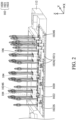
- FIG. 2 is a cross-sectional view of the power module 100 along the line A-A in FIG. 1 according to an embodiment of the present disclosure
- the power module 100 includes a substrate 102, at least one semiconductor component 104, a plurality of pins 106 and a package body 112.
- the substrate 102 is, for example, a ceramic substrate, which includes a base 1020, an electrical conductive layer 1021 and a thermal conductive layer 1022.
- the electrical conductive layer 1021 and the thermal conductive layer 1022 are arranged on opposite sides of the base 1020.
- the electrical conductive layer 1021 includes a plurality of electrical conductive portions 1024, and each of the electrical conductive portions 1024 has a first metal surface 1024S.
- the semiconductor component 104 may be a semiconductor chip, such as a power control chip, but it is not limited thereto.
- the semiconductor component 104 is disposed on the first metal surface 1024S.
- the plurality of pins 106 are configured so that the power module 100 can be plugged into an external connector or another electronic device (not shown in the figures).
- the plurality of pins 106 extend from the first metal surface 1024S, and the pins 106 are configured to be electrically connected to the semiconductor component 104.
- the package body 112 is configured to protect the semiconductor component 104 and the substrate 102.
- the package body 112 is made of insulating material, such as epoxy resin, but it is not limited thereto.
- the package body 112 is configured to cover the first metal surface 1024S and the aforementioned semiconductor component 104, and the package body 112 partially encloses each of the pins 106.
- the Comparative Tracking Index (CTI) of the package body 112 is greater than 400, but it is not limited thereto.
- CTI value of the package body 112 the industry generally has two types: 400 ⁇ 599 and > 600. The higher the value, the closer the distance between two conductors can be.
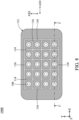
- FIG. 3 is a simplified top view of the power module 100 according to an embodiment of the present disclosure
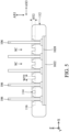
- FIG. 4 is a cross-sectional view of the power module 100 along line B-B in FIG. 3 according to an embodiment of the present disclosure.
- these pins 106 extend along a first axis AX1, and when viewed along the first axis AX1 (the Z-axis), these pins 106 are arranged in a matrix.
- the power module 100 can correspond to different types of connectors.
- the power module 100 can correspond to different types of connectors. Therefore, there is no need to design power modules with pins 106 in different arrangements for different types of connectors. Therefore, the cost of production is greatly reduced.
- these separating elements may include a plurality of first separating elements 114.
- Each first separating element 114 has a strip-shaped structure which extends along a second axis AX2, and the second axis AX2 is perpendicular to the first axis AX1.
- a total path length CS1 of the arrow in FIG. 4 is the creepage distance between two adjacent pins 106.
- the total path length CS1 is greater than the horizontal distance CS0 between the two adjacent pins 106 (along a third axis AX3). If the first separating element 114 is not provided, the creepage distance is equal to the horizontal distance CS0, and then the creepage distance may be too small to comply with the safety regulations. Therefore, providing the first separating element 114 can achieve the advantage of increasing the creepage distance.
- these first separating elements 114 are connected to the second separating elements 116, and these first separating elements 114 and the second separating elements 116 are staggered with each other.
- each of the first separating elements 114 and the second separating elements 116 is a rectangular protruding structure, and the width WT1 of the protruding structure is greater than or equal to 1 mm.
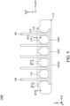
- FIG. 5 is a schematic cross-sectional view of a power module 100 according to another embodiment of the present disclosure.
- each of the first separating elements 114 and the second separating elements 116 may be a concave structure, and the width WT2 of the concave structure is greater than or equal to 1 mm.
- the height HT 1 of the protruding structure is also greater than or equal to 1 mm.
- the depth HT2 of the concave structure is also greater than or equal to 1 mm. Based on such a structural design, the creepage distance between two adjacent pins 106 can be effectively increased.
- the first separating elements 114, the second separating elements 116 and the package body 112 can be integrally formed as one piece, but they are not limited thereto.
- the materials of the first separating elements 114 and the second separating elements 116 may be different from the material of the package body 112.
- the first separating elements 114 and the second separating elements 116 can be made of elastic materials, and can be fixedly disposed on the package body 112 using glue or tape.
- the elastic materials may include rubber, for example, but it is not limited thereto.
- FIG. 6 and FIG. 7 are schematic cross-sectional views of simplified partial structures of a power module 100A according to different embodiments of the present disclosure.
- the first separating element 114 may have a first protruding structure 1141 and a second protruding structure 1142.
- the first protruding structure 1141 is disposed on the package body 112, and the second protruding structure 1142 is fixedly disposed on the first protruding structure 1141.
- the height HX1 of the first protruding structure 1141 is greater than or equal to 1 mm, and the height HX2 of the second protruding structure 1142 is greater than or equal to 1 mm.
- the width WX1 of the first protruding structure 1141 is greater than or equal to 2 mm, and the width WX2 of the second protruding structure 1142 is greater than or equal to 1 mm.
- the first separating element 114 has a first concave structure 1143 and a second concave structure 1144.
- the first concave structure 1143 is recessed along the first axis AX1 from the upper surface 112US of the package body 112, and the second concave structure 1144 is recessed from the first concave structure 1143 along the first axis AX1.
- the depth HX3 of the first concave structure 1143 is greater than or equal to 1 mm, and the depth HX4 of the second concave structure 1144 is greater than or equal to 1 mm.
- the width WX3 of the first concave structure 1143 is greater than or equal to 2 mm, and the width WX4 of the second concave structure 1144 is greater than or equal to 1 mm.
- FIG. 8 is a simplified top view of a power module 100B according to another embodiment of the present disclosure
- FIG. 9 is a schematic cross-sectional view of the power module 100B along line segment C-C in FIG. 8 according to another embodiment of the present disclosure.
- the package body 112 of the power module 100B can be further provided with four third separating elements 118, and when viewed along the first axis AX1, these four third separating elements 118 form a rectangle which surrounds the pins 106, the first separating elements 114, and the second separating elements 116.
- the four third separating elements 118 are connected to the first separating elements 114 and the second separating elements 116, but they are not limited thereto. In other embodiments, the third separating elements 118 may not be connected to the first separating elements 114 and the second separating elements 116.
- the first separating elements 114, the second separating elements 116 and the third separating elements 118 may be made of elastic materials, such as rubber material, but they are not limited thereto. That is, the material of the package body 112 is different from the materials of the first separating elements 114 , the second separating elements 116 and the third separating elements 118.
- the first separating elements 114, the second separating elements 116, the third separating elements 118 and the package body 112 may be integrally formed as one piece and made of an elastic material.
- each of these third separating elements 118 may also be a rectangular protruding structure, and the width WT3 of this protruding structure is greater than or equal to 1 mm. It is worth noting that the heights of the third separating element 118 and the first separating element 114 may be different. In this embodiment, the height HT3 of the third separating element 118 is less than the height HT1 of the first separating element 114, but the height HT3 is greater than or equal to 1 mm.
- FIG. 10 is a schematic cross-sectional view of the power module 100B according to another embodiment of the present disclosure.
- each of the third separating elements 118 is a concave structure, and the width WT4 of each of the third separating elements 118 is greater than or equal to 1 mm.
- the depth HT4 of the third separating element 118 is smaller than the depth HT2 of the first separating element 114, but the depth HT4 is greater than or equal to 1 mm.
- the thermal conductive layer 1022 of the substrate 102 has a second metal surface 1022S which is configured to dissipate the heat generated by the power module 100B to the external environment.
- the first metal surface 1024S and the second metal surface 1022S are located on opposite sides of the substrate 102, and a portion of the second metal surface 1022S is exposed from the package body 112 so as to increase the heat dissipation effect.
- FIG. 11 is a simplified top view of a power module 100C according to another embodiment of the present disclosure
- FIG. 12 is a schematic cross-sectional view of the power module 100C along line D-D in FIG. 11 according to another embodiment of the present disclosure.
- the power module 100C includes a first separating element 120 which is disposed on the package body 112 and surrounds the pins 106.
- these pins 106 extend along the first axis AX1, and when viewed along the first axis AX1, the first separating element 120 has two first strip-shaped portion 121 and two second strip-shaped portions 122.
- the two first strip-shaped portions 121 extend along the second axis AX2, and the two second strip-shaped portions 122 extend along the third axis AX3 .
- the first axis AX1, the second axis AX2 and the third axis AX3 are perpendicular to each other.
- each of the two first strip-shaped portions 121 and the two second strip-shaped portions 122 is a concave structure, similar to the third separating element 118 in FIG. 10 , and may have a depth HT4 and a width WT4, both of which are greater than or equal to 1 mm.
- the creepage distance between the outermost pin 106 and the bottom surface 112BS of the package body 112 can be effectively increased.
- FIG. 14 is a simplified top view of a power module 100D according to another embodiment of the present disclosure
- FIG. 15 is a schematic cross-sectional view of the power module 100D along line E-E in FIG. 14 according to another embodiment of the present disclosure.
- the power module 100D may further include at least a second separating element 124 which is disposed on one side of the first separating element 120, and the second separating element 124 extends along the second axis AX2.
- the width WT5 of the first separating element 120 and the width WT6 of the second separating element 124 are both greater than 1 mm, and as shown in FIG. 15 , the distance DS1 between the second separating element 124 and the first separating element 120 is greater than 1 mm.
- the power module 100D may further include at least a third separating element 126.
- the second separating element 124 is located between the first separating element 120 and the third separating element 126, and the third separating element 126 extends along the second axis AX2.
- the width WT7 of the third separating element 126 is greater than 1 mm, and the distance DS2 between the third separating element 126 and the second separating element 124 is greater than 1 mm.
- the distance DS2 may be equal to the distance DS1, but it is not limited thereto. In other embodiments, distance DS2 may be greater than distance DS1.
- each of the second separating elements 124 and the third separating elements 126 may be a protruding structure, and the width WT6 of the second separating element 124 is different from the width WT7 of the third separating element 126.
- the width WT7 of the third separating element 126 is greater than the width WT6 of the second separating element 124.
- FIG. 16 is a schematic cross-sectional view of the power module 100D according to another embodiment of the present disclosure.
- each of the second separating elements 124 and the third separating elements 126 is a concave structure.
- the creepage distance between the outermost pin 106 and the bottom surface of the package body 112 can be effectively increased.
- the first separating element 120, the second separating element 124 and the third separating element 126 are protruding structures, they may be made of elastic materials. Therefore, when the power module 100D is connected to an external connector, the buffering function can be effectively achieved so as to prevent the power module 100D from being damaged by excessive force.
- the present disclosure provides a power module having a substrate 102, a plurality of pins 106 and a package body 112. There is a gap SC between each two adjacent pins 106, and at least one separating element can be disposed in the gap SC to increase the creepage distance between two adjacent pins 106.
- the separating element can be a protruding structure or a concave structure, and the height and width of the protruding structure or the concave structure are greater than or equal to 1 mm.
- the separating element can be made of elastic materials, so that when the power module is connected to an external connector, the protruding separating element can serve as a buffering portion to prevent the power module from being damaged due to the excessive impact force.
Landscapes
- Structures Or Materials For Encapsulating Or Coating Semiconductor Devices Or Solid State Devices (AREA)
Abstract
Description
- This application claims the benefit of
China Patent Application No. 202311504356.4, filed on November 13, 2023 - The present disclosure relates to a power module, and in particular it relates to a power module that can reduce the volume.
- With the development of science and technology, many power modules are now quite popular and popular products.
- Generally speaking, a power module has a plurality of pins for signal transmission. However, in order to comply with safety regulations, the distance between adjacent pins is limited, making it very hard to reduce the overall size of the power module.
- Therefore, how to design a power module that can be reduced in size and comply with safety regulations are topics nowadays that need to be discussed and solved.
- Accordingly, one objective of the present disclosure is to provide a power module to solve the above problems.
- According to some embodiments of the disclosure, a power module is provided. The power module includes a substrate, a semiconductor component, a plurality of pins and a package body. The substrate has a first metal surface. The semiconductor component is disposed on the first metal surface. The plurality of pins extend from the first metal surface and are configured to be electrically connected to the semiconductor component. The package body is configured to cover the first metal surface and the semiconductor component, and the package body partially encloses each of the pins. There is a gap between each two adjacent pins, and a separating element is disposed in each gap to increase the creepage distance between two adjacent pins.
- According to some embodiments, the plurality of pins extends along a first axis, and when viewed along the first axis, the plurality of pins are arranged in a matrix.
- According to some embodiments, when viewed along the first axis, the separating elements include a plurality of first separating elements, each of the first separating elements has a strip-shaped structure which extends along a second axis, and the second axis is perpendicular to the first axis.
- According to some embodiments, when viewed along the first axis, the separating elements further include a plurality of second separating elements, each of the second separating elements has a strip-shaped structure which extends along a third axis, and the third axis is perpendicular to the first axis and the second axis.
- According to some embodiments, the first separating elements are connected to the second separating elements, and the first separating elements and the second separating elements are staggered with each other.
- According to some embodiments, each of the first separating elements is a protruding structure or a concave structure, and each of the second separating elements is a protruding structure or a concave structure.
- According to some embodiments, the width of the protruding structure or the concave structure is greater than or equal to 1 mm.
- According to some embodiments, the package body is further provided with four third separating elements, and when viewed along the first axis, the four third separating elements form a rectangle which surrounds the pins, the first separating elements and the second separating elements.
- According to some embodiments, the first separating elements, the second separating elements and the third separating elements are made of elastic materials, and the material of the package body is different from the materials of the first separating elements, the second separating elements and the third separating elements.
- According to some embodiments, each of the third separating elements is another protruding structure or another concave structure, and the width of each of the third separating elements is greater than or equal to 1 mm.
- According to some embodiments, the substrate further has a second metal surface configured to dissipate heat generated by the power module to the external environment, wherein the first metal surface and the second metal surface are located on opposite sides of the substrate, and a portion of the second metal surface is exposed from the package body.
- According to some embodiments, a power module is provided and includes a substrate, a semiconductor component, a plurality of pins, a package, and a first separating element. The substrate has a first metal surface. The semiconductor component is disposed on the first metal surface. The plurality of pins extends from the first metal surface and is configured to be electrically connected to the semiconductor component. The package body is configured to cover the first metal surface and the semiconductor component, and the package body partially encloses each of the pins. The first separating element is disposed on the package body and surrounds the pins.
- According to some embodiments, the pins extend along a first axis, and when viewed along the first axis, the first separating element has two first strip-shaped portions and two second strip-shaped portions, the two first strip-shaped portions extend along a second axis, and the two second strip-shaped portions extend along a third axis, where the first axis, the second axis and the third axis are perpendicular to each other.
- According to some embodiments, each of the two first strip-shaped portions and the two second strip-shaped portions is a protruding structure or a concave structure.
- According to some embodiments, the power module further includes a second separating element which is disposed on one side of the first separating element, and the second separating element extends along the second axis.
- According to some embodiments, the width of each first separating element and each second separating element is greater than 1 mm, and the distance between the second separating element and the first separating element is greater than 1 mm.
- According to some embodiments, the power module further includes a third separating element, the second separating element is located between the first separating element and the third separating element, and the third separating element extends along the second axis.
- According to some embodiments, the width of the third separating element is greater than 1 mm, and the distance between the third separating element and the second separating element is greater than 1 mm.
- According to some embodiments, the second separating element and the third separating element are each a protruding structure or a concave structure, and the width of the second separating element is different from the width of the third separating element.
- According to some embodiments, the first separating element, the second separating element and the third separating element are made of elastic materials.
- The present disclosure provides a power module having a substrate, a plurality of pins and a package body. There is a gap between each two adjacent pins, and at least one separating element can be disposed in each gap to increase the creepage distance between two adjacent pins. The separating element can be a protruding structure or a concave structure, and the height and width of the protruding structure or the concave structure are greater than or equal to 1 mm.
- Therefore, based on the design of the present disclosure, not only can the power module comply with safety regulations, but also the distance between two adjacent pins can be shortened, thereby reducing the overall size of the power module. In addition, the separating element can be made of elastic materials, so that when the power module is connected to an external connector, the protruding separating element can serve as a buffering portion to prevent the power module from being damaged due to the excessive impact force.
- Additional features and advantages of the disclosure will be set forth in the description which follows, and, in part, will be obvious from the description, or can be learned by practice of the principles disclosed herein. The features and advantages of the disclosure can be realized and obtained by means of the instruments and combinations pointed out in the appended claims. These and other features of the disclosure will become more fully apparent from the following description and appended claims, or can be learned by the practice of the principles set forth herein.
- Aspects of the present disclosure are best understood from the following detailed description when read with the accompanying figures. It is noted that, in accordance with the standard practice in the industry, various features are not drawn to scale. In fact, the dimensions of the various features may be arbitrarily increased or reduced for clarity of discussion.
-
FIG. 1 is a three-dimensional schematic diagram of apower module 100 according to an embodiment of the present disclosure. -
FIG. 2 is a cross-sectional view of thepower module 100 along the line A-A inFIG. 1 according to an embodiment of the present disclosure. -
FIG. 3 is a simplified top view of thepower module 100 according to an embodiment of the present disclosure. -
FIG. 4 is a cross-sectional view of thepower module 100 along line B-B inFIG. 3 according to an embodiment of the present disclosure. -
FIG. 5 is a schematic cross-sectional view of thepower module 100 according to another embodiment of the present disclosure. -
FIG. 6 andFIG. 7 are schematic cross-sectional views of simplified partial structures of apower module 100A according to different embodiments of the present disclosure. -
FIG. 8 is a simplified top view of apower module 100B according to another embodiment of the present disclosure. -
FIG. 9 is a schematic cross-sectional view of thepower module 100B along line segment C-C inFIG. 8 according to another embodiment of the present disclosure. -
FIG. 10 is a schematic cross-sectional view of thepower module 100B according to another embodiment of the present disclosure. -
FIG. 11 is a simplified top view of apower module 100C according to another embodiment of the present disclosure. -
FIG. 12 is a schematic cross-sectional view of thepower module 100C along line D-D inFIG. 11 according to another embodiment of the present disclosure. -
FIG. 13 is a schematic cross-sectional view of thepower module 100C according to another embodiment of the present disclosure. -
FIG. 14 is a simplified top view of apower module 100D according to another embodiment of the present disclosure. -
FIG. 15 is a schematic cross-sectional view of thepower module 100D along line E-E inFIG. 14 according to another embodiment of the present disclosure. -
FIG. 16 is a schematic cross-sectional view of thepower module 100D according to another embodiment of the present disclosure. - The following disclosure provides many different embodiments, or examples, for implementing different features of the provided subject matter. Specific examples of components and arrangements are described below to simplify the present disclosure. These are, of course, merely examples and are not intended to be limiting. For example, the formation of a first feature over or on a second feature in the description that follows may include embodiments in which the first and second features are in direct contact, and may also include embodiments in which additional features may be disposed between the first and second features, such that the first and second features may not be in direct contact.
- In addition, the present disclosure may repeat reference numerals and/or letters in the various examples. This repetition is for the purpose of simplicity and clarity and does not in itself dictate a relationship between the various embodiments and/or configurations discussed. Moreover, the formation of a feature on, connected to, and/or coupled to another feature in the present disclosure that follows may include embodiments in which the features are in direct contact, and may also include embodiments in which additional features may be disposed interposing the features, such that the features may not be in direct contact. In addition, spatially relative terms, for example, "vertical," "above," "over," "below,", "bottom," etc. as well as derivatives thereof (e.g., "downwardly," "upwardly," etc.) are used in the present disclosure for ease of description of one feature's relationship to another feature. The spatially relative terms are intended to cover different orientations of the device, including the features.
- Unless defined otherwise, all technical and scientific terms used herein have the same meaning as commonly understood by one of ordinary skill in the art to which this disclosure belongs. It should be appreciated that each term, which is defined in a commonly used dictionary, should be interpreted as having a meaning conforming to the relative skills and the background or the context of the present disclosure, and should not be interpreted in an idealized or overly formal manner unless defined otherwise.
- Use of ordinal terms such as "first", "second", etc., in the claims to modify a claim element does not by itself connote any priority, precedence, or order of one claim element over another or the temporal order in which acts of a method are performed, but are used merely as labels to distinguish one claim element having a certain name from another element having the same name (but for use of the ordinal term) to distinguish the claim elements.
- In addition, in some embodiments of the present disclosure, terms concerning attachments, coupling and the like, such as "connected" and "interconnected", refer to a relationship wherein structures are secured or attached to one another either directly or indirectly through intervening structures, as well as both movable or rigid attachments or relationships, unless expressly described otherwise.
- Please refer to
FIG. 1 andFIG. 2 .FIG. 1 is a three-dimensional schematic diagram of apower module 100 according to an embodiment of the present disclosure, andFIG. 2 is a cross-sectional view of thepower module 100 along the line A-A inFIG. 1 according to an embodiment of the present disclosure. In this embodiment, thepower module 100 includes asubstrate 102, at least onesemiconductor component 104, a plurality ofpins 106 and apackage body 112. - The
substrate 102 is, for example, a ceramic substrate, which includes abase 1020, an electricalconductive layer 1021 and a thermalconductive layer 1022. The electricalconductive layer 1021 and the thermalconductive layer 1022 are arranged on opposite sides of thebase 1020. The electricalconductive layer 1021 includes a plurality of electricalconductive portions 1024, and each of the electricalconductive portions 1024 has afirst metal surface 1024S. - The
semiconductor component 104 may be a semiconductor chip, such as a power control chip, but it is not limited thereto. Thesemiconductor component 104 is disposed on thefirst metal surface 1024S. Furthermore, the plurality ofpins 106 are configured so that thepower module 100 can be plugged into an external connector or another electronic device (not shown in the figures). The plurality ofpins 106 extend from thefirst metal surface 1024S, and thepins 106 are configured to be electrically connected to thesemiconductor component 104. - In addition, the
package body 112 is configured to protect thesemiconductor component 104 and thesubstrate 102. Thepackage body 112 is made of insulating material, such as epoxy resin, but it is not limited thereto. Thepackage body 112 is configured to cover thefirst metal surface 1024S and theaforementioned semiconductor component 104, and thepackage body 112 partially encloses each of thepins 106. In addition, the Comparative Tracking Index (CTI) of thepackage body 112 is greater than 400, but it is not limited thereto. Regarding the CTI value of thepackage body 112, the industry generally has two types: 400~599 and > 600. The higher the value, the closer the distance between two conductors can be. - Next, please refer to
FIG. 3 andFIG. 4 .FIG. 3 is a simplified top view of thepower module 100 according to an embodiment of the present disclosure, andFIG. 4 is a cross-sectional view of thepower module 100 along line B-B inFIG. 3 according to an embodiment of the present disclosure. As shown inFIG. 3 andFIG. 4 , thesepins 106 extend along a first axis AX1, and when viewed along the first axis AX1 (the Z-axis), thesepins 106 are arranged in a matrix. - Based on the arrangement of these
pins 106, thepower module 100 can correspond to different types of connectors. Thus, there is no need to design power modules withpins 106 in different arrangements for different types of connectors. Therefore, the cost of production is greatly reduced. - As shown in
FIG. 3 , there is a gap SC between each twoadjacent pins 106, and a separating element can be disposed in the gap SC to increase the creepage distance between twoadjacent pins 106. Specifically, when viewed along the first axis AX1, these separating elements may include a plurality offirst separating elements 114. Eachfirst separating element 114 has a strip-shaped structure which extends along a second axis AX2, and the second axis AX2 is perpendicular to the first axis AX1. - For example, a total path length CS1 of the arrow in
FIG. 4 is the creepage distance between twoadjacent pins 106. The total path length CS1 is greater than the horizontal distance CS0 between the two adjacent pins 106 (along a third axis AX3). If thefirst separating element 114 is not provided, the creepage distance is equal to the horizontal distance CS0, and then the creepage distance may be too small to comply with the safety regulations. Therefore, providing thefirst separating element 114 can achieve the advantage of increasing the creepage distance. - In addition, when viewed along the first axis AX1, these separating elements may further include a plurality of
second separating elements 116. Eachsecond separating element 116 has a strip-shaped structure which extends along the third axis AX3, and the third axis AX3 is perpendicular to the first axis AX1 and the second axis AX2. - As shown in
FIG. 3 , thesefirst separating elements 114 are connected to thesecond separating elements 116, and thesefirst separating elements 114 and thesecond separating elements 116 are staggered with each other. - In this embodiment, as shown in
FIG. 4 , each of thefirst separating elements 114 and thesecond separating elements 116 is a rectangular protruding structure, and the width WT1 of the protruding structure is greater than or equal to 1 mm. - The
first separating elements 114 and thesecond separating elements 116 are not limited to the protruding structures. As shown inFIG. 5 , FIG. 5 is a schematic cross-sectional view of apower module 100 according to another embodiment of the present disclosure. In this embodiment, each of thefirst separating elements 114 and thesecond separating elements 116 may be a concave structure, and the width WT2 of the concave structure is greater than or equal to 1 mm. - In addition, it should be noted that in
FIG. 4 , theheight HT 1 of the protruding structure is also greater than or equal to 1 mm. InFIG. 5 , the depth HT2 of the concave structure is also greater than or equal to 1 mm. Based on such a structural design, the creepage distance between twoadjacent pins 106 can be effectively increased. - Furthermore, in this embodiment, the
first separating elements 114, thesecond separating elements 116 and thepackage body 112 can be integrally formed as one piece, but they are not limited thereto. In other embodiments, the materials of thefirst separating elements 114 and thesecond separating elements 116 may be different from the material of thepackage body 112. For example, thefirst separating elements 114 and thesecond separating elements 116 can be made of elastic materials, and can be fixedly disposed on thepackage body 112 using glue or tape. The elastic materials may include rubber, for example, but it is not limited thereto. - Next, please refer to
FIG. 6 andFIG. 7 .FIG. 6 andFIG. 7 are schematic cross-sectional views of simplified partial structures of apower module 100A according to different embodiments of the present disclosure. InFIG. 6 , thefirst separating element 114 may have afirst protruding structure 1141 and asecond protruding structure 1142. Thefirst protruding structure 1141 is disposed on thepackage body 112, and thesecond protruding structure 1142 is fixedly disposed on thefirst protruding structure 1141. - The height HX1 of the
first protruding structure 1141 is greater than or equal to 1 mm, and the height HX2 of thesecond protruding structure 1142 is greater than or equal to 1 mm. Similarly, the width WX1 of thefirst protruding structure 1141 is greater than or equal to 2 mm, and the width WX2 of thesecond protruding structure 1142 is greater than or equal to 1 mm. - In
FIG. 7 , thefirst separating element 114 has a firstconcave structure 1143 and a secondconcave structure 1144. The firstconcave structure 1143 is recessed along the first axis AX1 from the upper surface 112US of thepackage body 112, and the secondconcave structure 1144 is recessed from the firstconcave structure 1143 along the first axis AX1. - The depth HX3 of the first
concave structure 1143 is greater than or equal to 1 mm, and the depth HX4 of the secondconcave structure 1144 is greater than or equal to 1 mm. Similarly, the width WX3 of the firstconcave structure 1143 is greater than or equal to 2 mm, and the width WX4 of the secondconcave structure 1144 is greater than or equal to 1 mm. - Next, please refer to
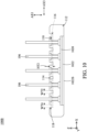
FIG. 8 andFIG. 9 at the same time.FIG. 8 is a simplified top view of apower module 100B according to another embodiment of the present disclosure, andFIG. 9 is a schematic cross-sectional view of thepower module 100B along line segment C-C inFIG. 8 according to another embodiment of the present disclosure. As shown inFIG. 8 andFIG. 9 , thepackage body 112 of thepower module 100B can be further provided with fourthird separating elements 118, and when viewed along the first axis AX1, these fourthird separating elements 118 form a rectangle which surrounds thepins 106, thefirst separating elements 114, and thesecond separating elements 116. - In this embodiment, the four
third separating elements 118 are connected to thefirst separating elements 114 and thesecond separating elements 116, but they are not limited thereto. In other embodiments, thethird separating elements 118 may not be connected to thefirst separating elements 114 and thesecond separating elements 116. - In addition, in this embodiment, the
first separating elements 114, thesecond separating elements 116 and thethird separating elements 118 may be made of elastic materials, such as rubber material, but they are not limited thereto. That is, the material of thepackage body 112 is different from the materials of thefirst separating elements 114 , thesecond separating elements 116 and thethird separating elements 118. In addition, in some embodiments, thefirst separating elements 114, thesecond separating elements 116, thethird separating elements 118 and thepackage body 112 may be integrally formed as one piece and made of an elastic material. - As shown in
FIG. 9 , each of thesethird separating elements 118 may also be a rectangular protruding structure, and the width WT3 of this protruding structure is greater than or equal to 1 mm. It is worth noting that the heights of thethird separating element 118 and thefirst separating element 114 may be different. In this embodiment, the height HT3 of thethird separating element 118 is less than the height HT1 of thefirst separating element 114, but the height HT3 is greater than or equal to 1 mm. - Similarly, the
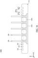
third separating element 118 is not limited to the protruding structure. As shown inFIG. 10, FIG. 10 is a schematic cross-sectional view of thepower module 100B according to another embodiment of the present disclosure. In this embodiment, each of thethird separating elements 118 is a concave structure, and the width WT4 of each of thethird separating elements 118 is greater than or equal to 1 mm. In addition, inFIG. 10 , the depth HT4 of thethird separating element 118 is smaller than the depth HT2 of thefirst separating element 114, but the depth HT4 is greater than or equal to 1 mm. - Furthermore, as shown in
FIG. 9 ,FIG. 10 andFIG. 2 , the thermalconductive layer 1022 of thesubstrate 102 has asecond metal surface 1022S which is configured to dissipate the heat generated by thepower module 100B to the external environment. Thefirst metal surface 1024S and thesecond metal surface 1022S are located on opposite sides of thesubstrate 102, and a portion of thesecond metal surface 1022S is exposed from thepackage body 112 so as to increase the heat dissipation effect. - Next, please refer to
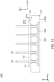
FIG. 11 andFIG. 12 at the same time.FIG. 11 is a simplified top view of apower module 100C according to another embodiment of the present disclosure, andFIG. 12 is a schematic cross-sectional view of thepower module 100C along line D-D inFIG. 11 according to another embodiment of the present disclosure. In this embodiment, thepower module 100C includes afirst separating element 120 which is disposed on thepackage body 112 and surrounds thepins 106. - As shown in
FIG. 11 andFIG. 12 , similar to the previous embodiments, thesepins 106 extend along the first axis AX1, and when viewed along the first axis AX1, thefirst separating element 120 has two first strip-shapedportion 121 and two second strip-shapedportions 122. The two first strip-shapedportions 121 extend along the second axis AX2, and the two second strip-shapedportions 122 extend along the third axis AX3 . The first axis AX1, the second axis AX2 and the third axis AX3 are perpendicular to each other. - In this embodiment, as shown in
FIG. 12 , the two first strip-shapedportions 121 and the two second strip-shapedportions 122 can be integrally formed as one piece, and each of the first strip-shapedportions 121 and the second strip-shapedportions 122 may be a rectangular protruding structure. The first strip-shapedportions 121 and the second strip-shapedportions 122 are similar to thethird separating element 118 inFIG. 9 , and may have a height HT3 and a width WT3, both of which are greater than or equal to 1 mm. - The first strip-shaped
portions 121 and the second strip-shapedportions 122 are not limited to the above protruding structures. As shown inFIG. 13, FIG. 13 is a schematic cross-sectional view of thepower module 100C according to another embodiment of the present disclosure. In this embodiment, each of the two first strip-shapedportions 121 and the two second strip-shapedportions 122 is a concave structure, similar to thethird separating element 118 inFIG. 10 , and may have a depth HT4 and a width WT4, both of which are greater than or equal to 1 mm. - Based on the design of the first strip-shaped
portions 121 and the second strip-shapedportions 122, the creepage distance between theoutermost pin 106 and the bottom surface 112BS of thepackage body 112 can be effectively increased. - Next, please refer to
FIG. 14 andFIG. 15 at the same time.FIG. 14 is a simplified top view of apower module 100D according to another embodiment of the present disclosure, andFIG. 15 is a schematic cross-sectional view of thepower module 100D along line E-E inFIG. 14 according to another embodiment of the present disclosure. Compared with thepower module 100C, thepower module 100D may further include at least asecond separating element 124 which is disposed on one side of thefirst separating element 120, and thesecond separating element 124 extends along the second axis AX2. - As shown in
FIG. 14 , the width WT5 of thefirst separating element 120 and the width WT6 of thesecond separating element 124 are both greater than 1 mm, and as shown inFIG. 15 , the distance DS1 between thesecond separating element 124 and thefirst separating element 120 is greater than 1 mm. - In addition, in this embodiment, the
power module 100D may further include at least athird separating element 126. Thesecond separating element 124 is located between thefirst separating element 120 and thethird separating element 126, and thethird separating element 126 extends along the second axis AX2. - In this embodiment, the width WT7 of the
third separating element 126 is greater than 1 mm, and the distance DS2 between thethird separating element 126 and thesecond separating element 124 is greater than 1 mm. In this embodiment, the distance DS2 may be equal to the distance DS1, but it is not limited thereto. In other embodiments, distance DS2 may be greater than distance DS1. - As shown in
FIG. 15 , each of thesecond separating elements 124 and thethird separating elements 126 may be a protruding structure, and the width WT6 of thesecond separating element 124 is different from the width WT7 of thethird separating element 126. For example, the width WT7 of thethird separating element 126 is greater than the width WT6 of thesecond separating element 124. - Similarly, the
second separating element 124 and thethird separating element 126 are not limited to the protruding structures. As shown inFIG. 16, FIG. 16 is a schematic cross-sectional view of thepower module 100D according to another embodiment of the present disclosure. In this embodiment, each of thesecond separating elements 124 and thethird separating elements 126 is a concave structure. - Based on the design of the
first separating element 120, thesecond separating element 124 and thethird separating element 126, the creepage distance between theoutermost pin 106 and the bottom surface of thepackage body 112 can be effectively increased. - Similar to the previous embodiments, when the
first separating element 120, thesecond separating element 124 and thethird separating element 126 are protruding structures, they may be made of elastic materials. Therefore, when thepower module 100D is connected to an external connector, the buffering function can be effectively achieved so as to prevent thepower module 100D from being damaged by excessive force. - In summary, the present disclosure provides a power module having a
substrate 102, a plurality ofpins 106 and apackage body 112. There is a gap SC between each twoadjacent pins 106, and at least one separating element can be disposed in the gap SC to increase the creepage distance between twoadjacent pins 106. The separating element can be a protruding structure or a concave structure, and the height and width of the protruding structure or the concave structure are greater than or equal to 1 mm. - Therefore, based on the design of the present disclosure, not only can the power module comply with safety regulations, but also the distance between two
adjacent pins 106 can be shortened, thereby reducing the overall size of the power module. In addition, the separating element can be made of elastic materials, so that when the power module is connected to an external connector, the protruding separating element can serve as a buffering portion to prevent the power module from being damaged due to the excessive impact force. - Although the embodiments and their advantages have been described in detail, it should be understood that various changes, substitutions, and alterations can be made herein without departing from the spirit and scope of the embodiments as defined by the appended claims. Moreover, the scope of the present application is not intended to be limited to the particular embodiments of the process, machine, manufacture, composition of matter, means, methods, and steps described in the specification. As one of ordinary skill in the art will readily appreciate from the disclosure, processes, machines, manufacture, compositions of matter, means, methods, or steps, presently existing or later to be developed, that perform substantially the same function or achieve substantially the same result as the corresponding embodiments described herein can be utilized according to the disclosure. Accordingly, the appended claims are intended to include within their scope such processes, machines, manufacture, compositions of matter, means, methods, or steps. In addition, each claim constitutes a separate embodiment, and the combination of various claims and embodiments are within the scope of the disclosure.
Claims (15)
- A power module (100), comprising:a substrate (102), having a first metal surface;a semiconductor component (104), disposed on the first metal surface;a plurality of pins (106), extending from the first metal surface and configured to be electrically connected to the semiconductor component; anda package body (112), configured to cover the first metal surface and the semiconductor component, wherein the package body partially encloses each of the pins,wherein there is a gap (SC) between each two adjacent pins, and a separating element (114) is disposed in each gap to increase a creepage distance between the two adjacent pins.
- The power module (100) as claimed in claim 1, wherein the plurality of pins (106) extend along a first axis (AX1), and when viewed along the first axis, the plurality of pins are arranged in a matrix.
- The power module (100) as claimed in claim 2, wherein when viewed along the first axis, the separating elements include a plurality of first separating elements (114; 120), each of the first separating elements has a strip-shaped structure which extends along a second axis (AX2), and the second axis is perpendicular to the first axis;
wherein when viewed along the first axis, the separating elements further include a plurality of second separating elements (116; 124), each of the second separating elements has a strip-shaped structure which extends along a third axis, and the third axis is perpendicular to the first axis and the second axis. - The power module (100) as claimed in claim 3, wherein the first separating elements are connected to the second separating elements, and the first separating elements and the second separating elements are staggered with each other;wherein each of the first separating elements is a protruding structure or a concave structure, and each of the second separating elements is a protruding structure or a concave structure;wherein a width of the protruding structure or the concave structure is greater than or equal to 1 mm.
- The power module (100) as claimed in claim 3 or 4, wherein the package body (112) is further provided with four third separating elements, and when viewed along the first axis, the four third separating elements form a rectangle which surrounds the pins, the first separating elements and the second separating elements.
- The power module (100) as claimed in claim 5, wherein the first separating elements, the second separating elements and the third separating elements are made of elastic materials, and material of the package body is different from the materials of the first separating elements, the second separating elements and the third separating elements.
- The power module (100) as claimed in claim 5 or 6, wherein each of the third separating elements is another protruding structure or another concave structure, and a width of each of the third separating elements is greater than or equal to 1 mm.
- The power module (100) as claimed in one of the preceding claims, wherein the substrate further has a second metal surface configured to dissipate heat generated by the power module to external environment, wherein the first metal surface and the second metal surface are located on opposite sides of the substrate, and a portion of the second metal surface is exposed from the package body.
- A power module (100; 100C), comprising:a substrate (102), having a first metal surface;a semiconductor component (104), disposed on the first metal surface;a plurality of pins (106), extending from the first metal surface and configured to be electrically connected to the semiconductor component;a package body (112), configured to cover the first metal surface and the semiconductor component, wherein the package body partially encloses each of the pins; anda first separating element (120), disposed on the package body (112) and surrounding the pins (106).
- The power module (100; 100C) as claimed in claim 9, wherein the pins extend along a first axis (AX1), and when viewed along the first axis, the first separating element has two first strip-shaped portions (121) and two second strip-shaped portions (122), the two first strip-shaped portions extend along a second axis (AX2), and the two second strip-shaped portions extend along a third axis (AX3), where the first axis, the second axis and the third axis are perpendicular to each other.
- The power module (100; 100C) as claimed in claim 10, wherein each of the two first strip-shaped portions and the two second strip-shaped portions is a protruding structure or a concave structure.
- The power module (100; 100D) as claimed in claim 10 or 11, wherein the power module further includes a second separating element (124) which is disposed on one side of the first separating element, and the second separating element extends along the second axis;wherein a width (WT5; WT6) of each of the first separating element and each of the second separating element is greater than 1 mm, and a distance between the second separating element and the first separating element is greater than 1 mm;wherein the power module further includes a third separating element (126), the second separating element is located between the first separating element and the third separating element, and the third separating element extends along the second axis.
- The power module (100; 100D) as claimed in claim 12, wherein a width (WT7) of the third separating element is greater than 1 mm, and a distance between the third separating element and the second separating element is greater than 1 mm.
- The power module (100; 100D) as claimed in claim 12 or 13, wherein the second separating element and the third separating element are each a protruding structure or a concave structure, and the width of the second separating element is different from a width of the third separating element.
- The power module (100; 100C; 100D) as claimed in one of claims 12-14, wherein the first separating element, the second separating element and the third separating element are made of elastic materials.
Priority Applications (1)
| Application Number | Priority Date | Filing Date | Title |
|---|---|---|---|
| EP26162059.5A EP4746680A2 (en) | 2023-11-13 | 2024-11-12 | PERFORMANCE MODULE |
Applications Claiming Priority (1)
| Application Number | Priority Date | Filing Date | Title |
|---|---|---|---|
| CN202311504356.4A CN119993919A (en) | 2023-11-13 | 2023-11-13 | Power Module |
Publications (2)
| Publication Number | Publication Date |
|---|---|
| EP4564419A2 true EP4564419A2 (en) | 2025-06-04 |
| EP4564419A3 EP4564419A3 (en) | 2025-09-03 |
Family
ID=93520658
Family Applications (2)
| Application Number | Title | Priority Date | Filing Date |
|---|---|---|---|
| EP24212450.1A Pending EP4564419A3 (en) | 2023-11-13 | 2024-11-12 | Power module |
| EP26162059.5A Pending EP4746680A2 (en) | 2023-11-13 | 2024-11-12 | PERFORMANCE MODULE |
Family Applications After (1)
| Application Number | Title | Priority Date | Filing Date |
|---|---|---|---|
| EP26162059.5A Pending EP4746680A2 (en) | 2023-11-13 | 2024-11-12 | PERFORMANCE MODULE |
Country Status (4)
| Country | Link |
|---|---|
| US (1) | US20250157863A1 (en) |
| EP (2) | EP4564419A3 (en) |
| JP (1) | JP2025080221A (en) |
| CN (1) | CN119993919A (en) |
Family Cites Families (9)
| Publication number | Priority date | Publication date | Assignee | Title |
|---|---|---|---|---|
| JP2003303939A (en) * | 2002-04-08 | 2003-10-24 | Hitachi Ltd | Power semiconductor device and inverter device |
| JP2007073743A (en) * | 2005-09-07 | 2007-03-22 | Denso Corp | Semiconductor device |
| JP5272768B2 (en) * | 2009-02-05 | 2013-08-28 | 三菱電機株式会社 | Power semiconductor device and manufacturing method thereof |
| JP5383621B2 (en) * | 2010-10-20 | 2014-01-08 | 三菱電機株式会社 | Power semiconductor device |
| US9839146B2 (en) * | 2015-10-20 | 2017-12-05 | Cree, Inc. | High voltage power module |
| CN210575896U (en) * | 2019-11-07 | 2020-05-19 | 常州瑞华新能源科技有限公司 | High Voltage Power Module Housing |
| WO2022021094A1 (en) * | 2020-07-28 | 2022-02-03 | 华为技术有限公司 | Power module, and preparation mold and apparatus |
| EP4057335A1 (en) * | 2021-03-10 | 2022-09-14 | Hitachi Energy Switzerland AG | Semiconductor package and manufacturing method |
| EP4195254A1 (en) * | 2021-12-10 | 2023-06-14 | Infineon Technologies AG | Housing, semiconductor module comprising a housing and method for producing a housing |
-
2023
- 2023-11-13 CN CN202311504356.4A patent/CN119993919A/en active Pending
-
2024
- 2024-06-20 US US18/748,531 patent/US20250157863A1/en active Pending
- 2024-10-15 JP JP2024179796A patent/JP2025080221A/en active Pending
- 2024-11-12 EP EP24212450.1A patent/EP4564419A3/en active Pending
- 2024-11-12 EP EP26162059.5A patent/EP4746680A2/en active Pending
Also Published As
| Publication number | Publication date |
|---|---|
| US20250157863A1 (en) | 2025-05-15 |
| EP4564419A3 (en) | 2025-09-03 |
| EP4746680A2 (en) | 2026-05-20 |
| JP2025080221A (en) | 2025-05-23 |
| CN119993919A (en) | 2025-05-13 |
Similar Documents
| Publication | Publication Date | Title |
|---|---|---|
| CN110544684B (en) | Thin-film encapsulation and encapsulation module including the same | |
| KR101874057B1 (en) | Integrated circuit package system with package stacking and method of manufacture thereof | |
| KR102677834B1 (en) | Semiconductor package | |
| CN104584209B (en) | Slim substrate PoP structures | |
| KR20110107766A (en) | Integrated circuit package system with stacking option and manufacturing method thereof | |
| US20170094830A1 (en) | Conformable thermal bridge | |
| CN103823280B (en) | Signal transmitting apparatus | |
| KR20130033808A (en) | Semiconductor package and method for manufacturing the same | |
| US12564058B2 (en) | Packaging architecture with reinforcement structure in package substrate | |
| TWI879223B (en) | Power module | |
| TWI767543B (en) | Package structure | |
| US20250157863A1 (en) | Power module | |
| US11908837B2 (en) | Semiconductor device | |
| US9397020B2 (en) | Semiconductor package | |
| US12550736B2 (en) | Packaging architecture with reinforcement structure in package substrate | |
| EP4407680A1 (en) | Chip packaging module and preparation method therefor, power supply module and electronic device | |
| KR102804101B1 (en) | Semiconductor package | |
| KR20230168752A (en) | Circuit board and semiconductor package having the same | |
| KR101255925B1 (en) | Semiconductor package and method for manufacturing the same | |
| CN223680095U (en) | Protective structure and optoelectronic chip packaging structure | |
| KR102728627B1 (en) | COF package | |
| US12620734B2 (en) | Optoelectronic component, network device, and method for manufacturing optoelectronic component | |
| US20250087651A1 (en) | Semiconductor package | |
| KR20200097316A (en) | Electronic package, terminal and electronic package processing method | |
| KR20260026473A (en) | Circuit boards and semiconductor packages including the same |
Legal Events
| Date | Code | Title | Description |
|---|---|---|---|
| PUAI | Public reference made under article 153(3) epc to a published international application that has entered the european phase |
Free format text: ORIGINAL CODE: 0009012 |
|
| STAA | Information on the status of an ep patent application or granted ep patent |
Free format text: STATUS: THE APPLICATION HAS BEEN PUBLISHED |
|
| AK | Designated contracting states |
Kind code of ref document: A2 Designated state(s): AL AT BE BG CH CY CZ DE DK EE ES FI FR GB GR HR HU IE IS IT LI LT LU LV MC ME MK MT NL NO PL PT RO RS SE SI SK SM TR |
|
| PUAL | Search report despatched |
Free format text: ORIGINAL CODE: 0009013 |
|
| AK | Designated contracting states |
Kind code of ref document: A3 Designated state(s): AL AT BE BG CH CY CZ DE DK EE ES FI FR GB GR HR HU IE IS IT LI LT LU LV MC ME MK MT NL NO PL PT RO RS SE SI SK SM TR |
|
| RIC1 | Information provided on ipc code assigned before grant |
Ipc: H01L 23/31 20060101AFI20250731BHEP Ipc: H01L 23/373 20060101ALI20250731BHEP Ipc: H01L 23/498 20060101ALI20250731BHEP Ipc: H01L 23/00 20060101ALI20250731BHEP Ipc: H01L 25/07 20060101ALI20250731BHEP |
|
| STAA | Information on the status of an ep patent application or granted ep patent |
Free format text: STATUS: REQUEST FOR EXAMINATION WAS MADE |
|
| 17P | Request for examination filed |
Effective date: 20260303 |